US11980090B2 - Compound and organic light emitting device comprising the same - Google Patents
Compound and organic light emitting device comprising the same Download PDFInfo
- Publication number
- US11980090B2 US11980090B2 US17/262,114 US201917262114A US11980090B2 US 11980090 B2 US11980090 B2 US 11980090B2 US 201917262114 A US201917262114 A US 201917262114A US 11980090 B2 US11980090 B2 US 11980090B2
- Authority
- US
- United States
- Prior art keywords
- compound
- group
- chemical formula
- light emitting
- har
- Prior art date
- Legal status (The legal status is an assumption and is not a legal conclusion. Google has not performed a legal analysis and makes no representation as to the accuracy of the status listed.)
- Active, expires
Links
- 150000001875 compounds Chemical class 0.000 title claims abstract description 99
- 239000000126 substance Substances 0.000 claims abstract description 116
- 239000011368 organic material Substances 0.000 claims description 42
- 125000003118 aryl group Chemical group 0.000 claims description 22
- 229910052760 oxygen Inorganic materials 0.000 claims description 19
- 229910052717 sulfur Inorganic materials 0.000 claims description 16
- 229910052739 hydrogen Inorganic materials 0.000 claims description 15
- 239000001257 hydrogen Substances 0.000 claims description 15
- 229910052705 radium Inorganic materials 0.000 claims description 15
- 229910052701 rubidium Inorganic materials 0.000 claims description 15
- 150000002431 hydrogen Chemical class 0.000 claims description 14
- 125000000217 alkyl group Chemical group 0.000 claims description 11
- 125000000753 cycloalkyl group Chemical group 0.000 claims description 9
- 125000001140 1,4-phenylene group Chemical group [H]C1=C([H])C([*:2])=C([H])C([H])=C1[*:1] 0.000 claims description 7
- TXCDCPKCNAJMEE-UHFFFAOYSA-N dibenzofuran Chemical group C1=CC=C2C3=CC=CC=C3OC2=C1 TXCDCPKCNAJMEE-UHFFFAOYSA-N 0.000 claims description 6
- IYYZUPMFVPLQIF-UHFFFAOYSA-N dibenzothiophene Chemical group C1=CC=C2C3=CC=CC=C3SC2=C1 IYYZUPMFVPLQIF-UHFFFAOYSA-N 0.000 claims description 6
- 125000001997 phenyl group Chemical group [H]C1=C([H])C([H])=C(*)C([H])=C1[H] 0.000 claims description 6
- FCEHBMOGCRZNNI-UHFFFAOYSA-N 1-benzothiophene Chemical group C1=CC=C2SC=CC2=C1 FCEHBMOGCRZNNI-UHFFFAOYSA-N 0.000 claims description 5
- 125000000732 arylene group Chemical group 0.000 claims description 5
- 125000006819 (C2-60) heteroaryl group Chemical group 0.000 claims description 3
- YZCKVEUIGOORGS-OUBTZVSYSA-N Deuterium Chemical compound [2H] YZCKVEUIGOORGS-OUBTZVSYSA-N 0.000 claims description 3
- 229910052805 deuterium Inorganic materials 0.000 claims description 3
- 125000001495 ethyl group Chemical group [H]C([H])([H])C([H])([H])* 0.000 claims description 3
- 125000005842 heteroatom Chemical group 0.000 claims description 3
- 229910052757 nitrogen Inorganic materials 0.000 claims description 3
- RFRXIWQYSOIBDI-UHFFFAOYSA-N benzarone Chemical group CCC=1OC2=CC=CC=C2C=1C(=O)C1=CC=C(O)C=C1 RFRXIWQYSOIBDI-UHFFFAOYSA-N 0.000 claims description 2
- 125000000843 phenylene group Chemical group C1(=C(C=CC=C1)*)* 0.000 claims description 2
- 239000010410 layer Substances 0.000 description 150
- -1 triethylsilyl group Chemical group 0.000 description 47
- 239000000463 material Substances 0.000 description 30
- 238000002347 injection Methods 0.000 description 28
- 239000007924 injection Substances 0.000 description 28
- 238000002360 preparation method Methods 0.000 description 28
- 230000032258 transport Effects 0.000 description 27
- 125000001424 substituent group Chemical group 0.000 description 22
- OKTJSMMVPCPJKN-UHFFFAOYSA-N Carbon Chemical compound [C] OKTJSMMVPCPJKN-UHFFFAOYSA-N 0.000 description 18
- 230000000903 blocking effect Effects 0.000 description 18
- 229910052799 carbon Inorganic materials 0.000 description 18
- 230000005525 hole transport Effects 0.000 description 17
- IANQTJSKSUMEQM-UHFFFAOYSA-N 1-benzofuran Chemical group C1=CC=C2OC=CC2=C1 IANQTJSKSUMEQM-UHFFFAOYSA-N 0.000 description 16
- 230000000052 comparative effect Effects 0.000 description 14
- 239000000758 substrate Substances 0.000 description 14
- 125000001072 heteroaryl group Chemical group 0.000 description 10
- 125000003003 spiro group Chemical group 0.000 description 9
- 229910052782 aluminium Inorganic materials 0.000 description 8
- XAGFODPZIPBFFR-UHFFFAOYSA-N aluminium Chemical compound [Al] XAGFODPZIPBFFR-UHFFFAOYSA-N 0.000 description 8
- 238000000034 method Methods 0.000 description 8
- VZSRBBMJRBPUNF-UHFFFAOYSA-N 2-(2,3-dihydro-1H-inden-2-ylamino)-N-[3-oxo-3-(2,4,6,7-tetrahydrotriazolo[4,5-c]pyridin-5-yl)propyl]pyrimidine-5-carboxamide Chemical compound C1C(CC2=CC=CC=C12)NC1=NC=C(C=N1)C(=O)NCCC(N1CC2=C(CC1)NN=N2)=O VZSRBBMJRBPUNF-UHFFFAOYSA-N 0.000 description 7
- 125000003342 alkenyl group Chemical group 0.000 description 7
- 238000006243 chemical reaction Methods 0.000 description 7
- 238000000151 deposition Methods 0.000 description 7
- PQXKHYXIUOZZFA-UHFFFAOYSA-M lithium fluoride Chemical compound [Li+].[F-] PQXKHYXIUOZZFA-UHFFFAOYSA-M 0.000 description 7
- XLYOFNOQVPJJNP-UHFFFAOYSA-N water Substances O XLYOFNOQVPJJNP-UHFFFAOYSA-N 0.000 description 7
- 150000004982 aromatic amines Chemical class 0.000 description 6
- 239000010406 cathode material Substances 0.000 description 6
- YTPLMLYBLZKORZ-UHFFFAOYSA-N Thiophene Chemical group C=1C=CSC=1 YTPLMLYBLZKORZ-UHFFFAOYSA-N 0.000 description 5
- 239000010405 anode material Substances 0.000 description 5
- 239000012153 distilled water Substances 0.000 description 5
- 230000000694 effects Effects 0.000 description 5
- 229910052751 metal Inorganic materials 0.000 description 5
- 239000002184 metal Substances 0.000 description 5
- AFCARXCZXQIEQB-UHFFFAOYSA-N N-[3-oxo-3-(2,4,6,7-tetrahydrotriazolo[4,5-c]pyridin-5-yl)propyl]-2-[[3-(trifluoromethoxy)phenyl]methylamino]pyrimidine-5-carboxamide Chemical compound O=C(CCNC(=O)C=1C=NC(=NC=1)NCC1=CC(=CC=C1)OC(F)(F)F)N1CC2=C(CC1)NN=N2 AFCARXCZXQIEQB-UHFFFAOYSA-N 0.000 description 4
- WYURNTSHIVDZCO-UHFFFAOYSA-N Tetrahydrofuran Chemical compound C1CCOC1 WYURNTSHIVDZCO-UHFFFAOYSA-N 0.000 description 4
- 125000004432 carbon atom Chemical group C* 0.000 description 4
- 125000004093 cyano group Chemical group *C#N 0.000 description 4
- 125000004185 ester group Chemical group 0.000 description 4
- 125000004433 nitrogen atom Chemical group N* 0.000 description 4
- 239000012044 organic layer Substances 0.000 description 4
- YIWGJFPJRAEKMK-UHFFFAOYSA-N 1-(2H-benzotriazol-5-yl)-3-methyl-8-[2-[[3-(trifluoromethoxy)phenyl]methylamino]pyrimidine-5-carbonyl]-1,3,8-triazaspiro[4.5]decane-2,4-dione Chemical compound CN1C(=O)N(c2ccc3n[nH]nc3c2)C2(CCN(CC2)C(=O)c2cnc(NCc3cccc(OC(F)(F)F)c3)nc2)C1=O YIWGJFPJRAEKMK-UHFFFAOYSA-N 0.000 description 3
- QJWNBZVEFVDEGZ-UHFFFAOYSA-N 2-(4'-bromospiro[fluorene-9,6'-indeno[1,2-e][1]benzofuran]-2-yl)-4,6-diphenyl-1,3,5-triazine Chemical compound C1=CC=C(C=C1)C2=NC(=NC(=N2)C3=CC4=C(C=C3)C5=CC=CC=C5C46C7=CC=CC=C7C8=C9C=COC9=C(C=C68)Br)C1=CC=CC=C1 QJWNBZVEFVDEGZ-UHFFFAOYSA-N 0.000 description 3
- DDGPPAMADXTGTN-UHFFFAOYSA-N 2-chloro-4,6-diphenyl-1,3,5-triazine Chemical compound N=1C(Cl)=NC(C=2C=CC=CC=2)=NC=1C1=CC=CC=C1 DDGPPAMADXTGTN-UHFFFAOYSA-N 0.000 description 3
- CSCPPACGZOOCGX-UHFFFAOYSA-N Acetone Chemical compound CC(C)=O CSCPPACGZOOCGX-UHFFFAOYSA-N 0.000 description 3
- ZOXJGFHDIHLPTG-UHFFFAOYSA-N Boron Chemical group [B] ZOXJGFHDIHLPTG-UHFFFAOYSA-N 0.000 description 3
- XEKOWRVHYACXOJ-UHFFFAOYSA-N Ethyl acetate Chemical compound CCOC(C)=O XEKOWRVHYACXOJ-UHFFFAOYSA-N 0.000 description 3
- YLQBMQCUIZJEEH-UHFFFAOYSA-N Furan Chemical group C=1C=COC=1 YLQBMQCUIZJEEH-UHFFFAOYSA-N 0.000 description 3
- KFZMGEQAYNKOFK-UHFFFAOYSA-N Isopropanol Chemical compound CC(C)O KFZMGEQAYNKOFK-UHFFFAOYSA-N 0.000 description 3
- OKKJLVBELUTLKV-UHFFFAOYSA-N Methanol Chemical compound OC OKKJLVBELUTLKV-UHFFFAOYSA-N 0.000 description 3
- MKYBYDHXWVHEJW-UHFFFAOYSA-N N-[1-oxo-1-(2,4,6,7-tetrahydrotriazolo[4,5-c]pyridin-5-yl)propan-2-yl]-2-[[3-(trifluoromethoxy)phenyl]methylamino]pyrimidine-5-carboxamide Chemical compound O=C(C(C)NC(=O)C=1C=NC(=NC=1)NCC1=CC(=CC=C1)OC(F)(F)F)N1CC2=C(CC1)NN=N2 MKYBYDHXWVHEJW-UHFFFAOYSA-N 0.000 description 3
- BQCADISMDOOEFD-UHFFFAOYSA-N Silver Chemical compound [Ag] BQCADISMDOOEFD-UHFFFAOYSA-N 0.000 description 3
- 125000002877 alkyl aryl group Chemical group 0.000 description 3
- 239000000956 alloy Substances 0.000 description 3
- 229910045601 alloy Inorganic materials 0.000 description 3
- 125000003710 aryl alkyl group Chemical group 0.000 description 3
- 125000001769 aryl amino group Chemical group 0.000 description 3
- 125000006267 biphenyl group Chemical group 0.000 description 3
- 125000002915 carbonyl group Chemical group [*:2]C([*:1])=O 0.000 description 3
- 238000000576 coating method Methods 0.000 description 3
- 229940125904 compound 1 Drugs 0.000 description 3
- 229920001940 conductive polymer Polymers 0.000 description 3
- 230000008021 deposition Effects 0.000 description 3
- 125000000623 heterocyclic group Chemical group 0.000 description 3
- 238000004770 highest occupied molecular orbital Methods 0.000 description 3
- RAXXELZNTBOGNW-UHFFFAOYSA-N imidazole Natural products C1=CNC=N1 RAXXELZNTBOGNW-UHFFFAOYSA-N 0.000 description 3
- 125000005462 imide group Chemical group 0.000 description 3
- 238000004519 manufacturing process Methods 0.000 description 3
- 150000002739 metals Chemical class 0.000 description 3
- 229910052709 silver Inorganic materials 0.000 description 3
- 239000004332 silver Substances 0.000 description 3
- 125000003808 silyl group Chemical group [H][Si]([H])([H])[*] 0.000 description 3
- 239000007787 solid Substances 0.000 description 3
- 239000000243 solution Substances 0.000 description 3
- 239000010409 thin film Substances 0.000 description 3
- QFLWZFQWSBQYPS-AWRAUJHKSA-N (3S)-3-[[(2S)-2-[[(2S)-2-[5-[(3aS,6aR)-2-oxo-1,3,3a,4,6,6a-hexahydrothieno[3,4-d]imidazol-4-yl]pentanoylamino]-3-methylbutanoyl]amino]-3-(4-hydroxyphenyl)propanoyl]amino]-4-[1-bis(4-chlorophenoxy)phosphorylbutylamino]-4-oxobutanoic acid Chemical compound CCCC(NC(=O)[C@H](CC(O)=O)NC(=O)[C@H](Cc1ccc(O)cc1)NC(=O)[C@@H](NC(=O)CCCCC1SC[C@@H]2NC(=O)N[C@H]12)C(C)C)P(=O)(Oc1ccc(Cl)cc1)Oc1ccc(Cl)cc1 QFLWZFQWSBQYPS-AWRAUJHKSA-N 0.000 description 2
- 125000005916 2-methylpentyl group Chemical group 0.000 description 2
- CBEVPIOKQWGLCD-UHFFFAOYSA-N CC1(OB(OC1(C)C)C1=CC=2C3(C=4C=CC=CC=4C=2C2=C1OC1=C2C=CC=C1)C1=CC=CC=C1C=1C=CC(=CC=13)C#N)C Chemical compound CC1(OB(OC1(C)C)C1=CC=2C3(C=4C=CC=CC=4C=2C2=C1OC1=C2C=CC=C1)C1=CC=CC=C1C=1C=CC(=CC=13)C#N)C CBEVPIOKQWGLCD-UHFFFAOYSA-N 0.000 description 2
- OYPRJOBELJOOCE-UHFFFAOYSA-N Calcium Chemical compound [Ca] OYPRJOBELJOOCE-UHFFFAOYSA-N 0.000 description 2
- GYHNNYVSQQEPJS-UHFFFAOYSA-N Gallium Chemical compound [Ga] GYHNNYVSQQEPJS-UHFFFAOYSA-N 0.000 description 2
- WHXSMMKQMYFTQS-UHFFFAOYSA-N Lithium Chemical compound [Li] WHXSMMKQMYFTQS-UHFFFAOYSA-N 0.000 description 2
- NIPNSKYNPDTRPC-UHFFFAOYSA-N N-[2-oxo-2-(2,4,6,7-tetrahydrotriazolo[4,5-c]pyridin-5-yl)ethyl]-2-[[3-(trifluoromethoxy)phenyl]methylamino]pyrimidine-5-carboxamide Chemical compound O=C(CNC(=O)C=1C=NC(=NC=1)NCC1=CC(=CC=C1)OC(F)(F)F)N1CC2=C(CC1)NN=N2 NIPNSKYNPDTRPC-UHFFFAOYSA-N 0.000 description 2
- KDLHZDBZIXYQEI-UHFFFAOYSA-N Palladium Chemical compound [Pd] KDLHZDBZIXYQEI-UHFFFAOYSA-N 0.000 description 2
- FAPWRFPIFSIZLT-UHFFFAOYSA-M Sodium chloride Chemical compound [Na+].[Cl-] FAPWRFPIFSIZLT-UHFFFAOYSA-M 0.000 description 2
- 238000006069 Suzuki reaction reaction Methods 0.000 description 2
- 239000007983 Tris buffer Substances 0.000 description 2
- HCHKCACWOHOZIP-UHFFFAOYSA-N Zinc Chemical compound [Zn] HCHKCACWOHOZIP-UHFFFAOYSA-N 0.000 description 2
- 230000009471 action Effects 0.000 description 2
- 125000003282 alkyl amino group Chemical group 0.000 description 2
- MWPLVEDNUUSJAV-UHFFFAOYSA-N anthracene Chemical compound C1=CC=CC2=CC3=CC=CC=C3C=C21 MWPLVEDNUUSJAV-UHFFFAOYSA-N 0.000 description 2
- 125000005264 aryl amine group Chemical group 0.000 description 2
- QVGXLLKOCUKJST-UHFFFAOYSA-N atomic oxygen Chemical compound [O] QVGXLLKOCUKJST-UHFFFAOYSA-N 0.000 description 2
- 229910052791 calcium Inorganic materials 0.000 description 2
- 239000011575 calcium Substances 0.000 description 2
- 125000000609 carbazolyl group Chemical group C1(=CC=CC=2C3=CC=CC=C3NC12)* 0.000 description 2
- WDECIBYCCFPHNR-UHFFFAOYSA-N chrysene Chemical compound C1=CC=CC2=CC=C3C4=CC=CC=C4C=CC3=C21 WDECIBYCCFPHNR-UHFFFAOYSA-N 0.000 description 2
- 229940125773 compound 10 Drugs 0.000 description 2
- 229940125782 compound 2 Drugs 0.000 description 2
- 229940126214 compound 3 Drugs 0.000 description 2
- 229940125898 compound 5 Drugs 0.000 description 2
- 150000004696 coordination complex Chemical class 0.000 description 2
- 239000003599 detergent Substances 0.000 description 2
- 239000002019 doping agent Substances 0.000 description 2
- GVEPBJHOBDJJJI-UHFFFAOYSA-N fluoranthrene Natural products C1=CC(C2=CC=CC=C22)=C3C2=CC=CC3=C1 GVEPBJHOBDJJJI-UHFFFAOYSA-N 0.000 description 2
- 125000003983 fluorenyl group Chemical group C1(=CC=CC=2C3=CC=CC=C3CC12)* 0.000 description 2
- 229910052733 gallium Inorganic materials 0.000 description 2
- 125000005843 halogen group Chemical group 0.000 description 2
- 125000005241 heteroarylamino group Chemical group 0.000 description 2
- AMGQUBHHOARCQH-UHFFFAOYSA-N indium;oxotin Chemical class [In].[Sn]=O AMGQUBHHOARCQH-UHFFFAOYSA-N 0.000 description 2
- ZLVXBBHTMQJRSX-VMGNSXQWSA-N jdtic Chemical compound C1([C@]2(C)CCN(C[C@@H]2C)C[C@H](C(C)C)NC(=O)[C@@H]2NCC3=CC(O)=CC=C3C2)=CC=CC(O)=C1 ZLVXBBHTMQJRSX-VMGNSXQWSA-N 0.000 description 2
- 229910052744 lithium Inorganic materials 0.000 description 2
- 229910044991 metal oxide Inorganic materials 0.000 description 2
- 150000004706 metal oxides Chemical class 0.000 description 2
- 125000002950 monocyclic group Chemical group 0.000 description 2
- WCPAKWJPBJAGKN-UHFFFAOYSA-N oxadiazole Chemical group C1=CON=N1 WCPAKWJPBJAGKN-UHFFFAOYSA-N 0.000 description 2
- 239000001301 oxygen Substances 0.000 description 2
- 125000002080 perylenyl group Chemical group C1(=CC=C2C=CC=C3C4=CC=CC5=CC=CC(C1=C23)=C45)* 0.000 description 2
- 238000005240 physical vapour deposition Methods 0.000 description 2
- BASFCYQUMIYNBI-UHFFFAOYSA-N platinum Chemical compound [Pt] BASFCYQUMIYNBI-UHFFFAOYSA-N 0.000 description 2
- 229920000767 polyaniline Polymers 0.000 description 2
- 125000003367 polycyclic group Chemical group 0.000 description 2
- BWHMMNNQKKPAPP-UHFFFAOYSA-L potassium carbonate Chemical compound [K+].[K+].[O-]C([O-])=O BWHMMNNQKKPAPP-UHFFFAOYSA-L 0.000 description 2
- BBEAQIROQSPTKN-UHFFFAOYSA-N pyrene Chemical compound C1=CC=C2C=CC3=CC=CC4=CC=C1C2=C43 BBEAQIROQSPTKN-UHFFFAOYSA-N 0.000 description 2
- 230000004044 response Effects 0.000 description 2
- 239000002356 single layer Substances 0.000 description 2
- PUZPDOWCWNUUKD-UHFFFAOYSA-M sodium fluoride Chemical compound [F-].[Na+] PUZPDOWCWNUUKD-UHFFFAOYSA-M 0.000 description 2
- 125000001973 tert-pentyl group Chemical group [H]C([H])([H])C([H])([H])C(*)(C([H])([H])[H])C([H])([H])[H] 0.000 description 2
- 229930192474 thiophene Natural products 0.000 description 2
- XOLBLPGZBRYERU-UHFFFAOYSA-N tin dioxide Chemical compound O=[Sn]=O XOLBLPGZBRYERU-UHFFFAOYSA-N 0.000 description 2
- 229910052725 zinc Inorganic materials 0.000 description 2
- 239000011701 zinc Substances 0.000 description 2
- 235000014692 zinc oxide Nutrition 0.000 description 2
- GHYOCDFICYLMRF-UTIIJYGPSA-N (2S,3R)-N-[(2S)-3-(cyclopenten-1-yl)-1-[(2R)-2-methyloxiran-2-yl]-1-oxopropan-2-yl]-3-hydroxy-3-(4-methoxyphenyl)-2-[[(2S)-2-[(2-morpholin-4-ylacetyl)amino]propanoyl]amino]propanamide Chemical compound C1(=CCCC1)C[C@@H](C(=O)[C@@]1(OC1)C)NC([C@H]([C@@H](C1=CC=C(C=C1)OC)O)NC([C@H](C)NC(CN1CCOCC1)=O)=O)=O GHYOCDFICYLMRF-UTIIJYGPSA-N 0.000 description 1
- AFBZMKWCZFFWIC-HVEFNXCZSA-N (3s)-3-[[(2s)-2-[[(2s)-2-[[(2r)-2-[[(2s)-2-[[(2s)-2-[[(2s)-2-amino-3-methylbutanoyl]amino]-3-(4-hydroxyphenyl)propanoyl]amino]-3-(4-hydroxyphenyl)propanoyl]amino]-3-sulfanylpropanoyl]amino]-3-(1h-imidazol-5-yl)propanoyl]amino]-4-methylpentanoyl]amino]-4-[ Chemical compound C([C@@H](C(=O)N[C@@H](CC(C)C)C(=O)N[C@@H](CC(O)=O)C(=O)N[C@@H]([C@@H](C)CC)C(=O)N[C@@H]([C@@H](C)CC)C(=O)N[C@@H](CC=1C2=CC=CC=C2NC=1)C(O)=O)NC(=O)[C@H](CS)NC(=O)[C@H](CC=1C=CC(O)=CC=1)NC(=O)[C@H](CC=1C=CC(O)=CC=1)NC(=O)[C@@H](N)C(C)C)C1=CNC=N1 AFBZMKWCZFFWIC-HVEFNXCZSA-N 0.000 description 1
- CEBAHYWORUOILU-UHFFFAOYSA-N (4-cyanophenyl)boronic acid Chemical compound OB(O)C1=CC=C(C#N)C=C1 CEBAHYWORUOILU-UHFFFAOYSA-N 0.000 description 1
- 125000000008 (C1-C10) alkyl group Chemical group 0.000 description 1
- UWRZIZXBOLBCON-VOTSOKGWSA-N (e)-2-phenylethenamine Chemical compound N\C=C\C1=CC=CC=C1 UWRZIZXBOLBCON-VOTSOKGWSA-N 0.000 description 1
- JYEUMXHLPRZUAT-UHFFFAOYSA-N 1,2,3-triazine Chemical group C1=CN=NN=C1 JYEUMXHLPRZUAT-UHFFFAOYSA-N 0.000 description 1
- YJTKZCDBKVTVBY-UHFFFAOYSA-N 1,3-Diphenylbenzene Chemical group C1=CC=CC=C1C1=CC=CC(C=2C=CC=CC=2)=C1 YJTKZCDBKVTVBY-UHFFFAOYSA-N 0.000 description 1
- 125000000355 1,3-benzoxazolyl group Chemical group O1C(=NC2=C1C=CC=C2)* 0.000 description 1
- 125000004973 1-butenyl group Chemical group C(=CCC)* 0.000 description 1
- 125000006218 1-ethylbutyl group Chemical group [H]C([H])([H])C([H])([H])C([H])([H])C([H])(*)C([H])([H])C([H])([H])[H] 0.000 description 1
- 125000006023 1-pentenyl group Chemical group 0.000 description 1
- 125000006017 1-propenyl group Chemical group 0.000 description 1
- HRQKKRRJWHNSKA-UHFFFAOYSA-N 11-(4,4,5,5-tetramethyl-1,3,2-dioxaborolan-2-yl)spiro[9-thiapentacyclo[11.7.0.02,10.03,8.015,20]icosa-1(13),2(10),3,5,7,11,15,17,19-nonaene-14,9'-fluorene]-3'-carbonitrile Chemical compound CC1(OB(OC1(C)C)C1=CC2=C(C=3C=CC=CC3C23C2=CC=CC=C2C=2C=C(C=CC32)C#N)C=3C2=C(SC31)C=CC=C2)C HRQKKRRJWHNSKA-UHFFFAOYSA-N 0.000 description 1
- MYKQKWIPLZEVOW-UHFFFAOYSA-N 11h-benzo[a]carbazole Chemical group C1=CC2=CC=CC=C2C2=C1C1=CC=CC=C1N2 MYKQKWIPLZEVOW-UHFFFAOYSA-N 0.000 description 1
- RRPLVAILDXQQCX-UHFFFAOYSA-N 14-phenyl-14-[4-(4,4,5,5-tetramethyl-1,3,2-dioxaborolan-2-yl)phenyl]-9-oxapentacyclo[11.7.0.02,10.03,8.015,20]icosa-1(13),2(10),3(8),4,6,11,15(20),16,18-nonaene-5,17-dicarbonitrile Chemical compound B1(OC(C(O1)(C)C)(C)C)C2=CC=C(C=C2)C3(C4=C(C5=C3C=C(C=C5)C#N)C6=C(C=C4)OC7=C6C=C(C=C7)C#N)C8=CC=CC=C8 RRPLVAILDXQQCX-UHFFFAOYSA-N 0.000 description 1
- QWENRTYMTSOGBR-UHFFFAOYSA-N 1H-1,2,3-Triazole Chemical group C=1C=NNN=1 QWENRTYMTSOGBR-UHFFFAOYSA-N 0.000 description 1
- HYZJCKYKOHLVJF-UHFFFAOYSA-N 1H-benzimidazole Chemical group C1=CC=C2NC=NC2=C1 HYZJCKYKOHLVJF-UHFFFAOYSA-N 0.000 description 1
- PAZAMICWXGKQOJ-UHFFFAOYSA-N 2-(4'-bromospiro[fluorene-9,6'-indeno[1,2-e][1]benzothiole]-2-yl)-4,6-diphenyl-1,3,5-triazine Chemical compound C1=CC=C(C=C1)C2=NC(=NC(=N2)C3=CC4=C(C=C3)C5=CC=CC=C5C46C7=CC=CC=C7C8=C9C=CSC9=C(C=C68)Br)C1=CC=CC=C1 PAZAMICWXGKQOJ-UHFFFAOYSA-N 0.000 description 1
- MWFMAUIICUHYLR-UHFFFAOYSA-N 2-(4-bromospiro[9-thiapentacyclo[11.7.0.02,10.03,8.015,20]icosa-1(13),2(10),3(8),4,6,11,15,17,19-nonaene-14,9'-fluorene]-2'-yl)-1-phenylbenzimidazole Chemical compound C1=CC=C(C=C1)N2C3=CC=CC=C3N=C2C4=CC5=C(C=C4)C6=CC=CC=C6C57C8=C(C9=CC=CC=C79)C1=C(C=C8)SC2=C1C(=CC=C2)Br MWFMAUIICUHYLR-UHFFFAOYSA-N 0.000 description 1
- 125000004974 2-butenyl group Chemical group C(C=CC)* 0.000 description 1
- QHCCOYAKYCWDOJ-UHFFFAOYSA-N 2-ethyl-1h-benzimidazole Chemical compound C1=CC=C2NC(CC)=NC2=C1 QHCCOYAKYCWDOJ-UHFFFAOYSA-N 0.000 description 1
- 125000006176 2-ethylbutyl group Chemical group [H]C([H])([H])C([H])([H])C([H])(C([H])([H])*)C([H])([H])C([H])([H])[H] 0.000 description 1
- 125000006024 2-pentenyl group Chemical group 0.000 description 1
- 125000003903 2-propenyl group Chemical group [H]C([*])([H])C([H])=C([H])[H] 0.000 description 1
- 125000004975 3-butenyl group Chemical group C(CC=C)* 0.000 description 1
- 125000006027 3-methyl-1-butenyl group Chemical group 0.000 description 1
- DQICCJAQPLMHCH-UHFFFAOYSA-N 4-(11-fluoro-14-phenyl-9-oxapentacyclo[11.7.0.02,10.03,8.015,20]icosa-1,3,5,7,10,12,15,17,19-nonaen-14-yl)benzonitrile Chemical compound FC1=CC=2C(C=3C=CC=CC3C2C2=C1OC1=C2C=CC=C1)(C1=CC=CC=C1)C1=CC=C(C#N)C=C1 DQICCJAQPLMHCH-UHFFFAOYSA-N 0.000 description 1
- DDTHMESPCBONDT-UHFFFAOYSA-N 4-(4-oxocyclohexa-2,5-dien-1-ylidene)cyclohexa-2,5-dien-1-one Chemical compound C1=CC(=O)C=CC1=C1C=CC(=O)C=C1 DDTHMESPCBONDT-UHFFFAOYSA-N 0.000 description 1
- 125000004920 4-methyl-2-pentyl group Chemical group CC(CC(C)*)C 0.000 description 1
- WPCWYOQYOZNISV-UHFFFAOYSA-N 6-(4,4,5,5-tetramethyl-1,3,2-dioxaborolan-2-yl)spiro[9-oxapentacyclo[11.7.0.02,10.03,8.015,20]icosa-1(13),2(10),3(8),4,6,11,15(20),16,18-nonaene-14,9'-fluorene]-5,17-dicarbonitrile Chemical compound B1(OC(C(O1)(C)C)(C)C)C2=CC3=C(C=C2C#N)C4=C(O3)C=CC5=C4C6=C(C57C8=CC=CC=C8C9=CC=CC=C79)C=C(C=C6)C#N WPCWYOQYOZNISV-UHFFFAOYSA-N 0.000 description 1
- CGVVACGFIALGLL-UHFFFAOYSA-N 6-phenyl-6-[4-(4,4,5,5-tetramethyl-1,3,2-dioxaborolan-2-yl)phenyl]indeno[1,2-e][1]benzothiole-1,8-dicarbonitrile Chemical compound B1(OC(C(O1)(C)C)(C)C)C2=CC=C(C=C2)C3(C4=C(C5=C3C=C(C=C5)C#N)C6=C(C=C4)SC=C6C#N)C7=CC=CC=C7 CGVVACGFIALGLL-UHFFFAOYSA-N 0.000 description 1
- ZCYVEMRRCGMTRW-UHFFFAOYSA-N 7553-56-2 Chemical compound [I] ZCYVEMRRCGMTRW-UHFFFAOYSA-N 0.000 description 1
- GGGMNYRKOLIASC-UHFFFAOYSA-N 8'-bromospiro[fluorene-9,6'-indeno[1,2-e][1]benzofuran]-4'-carbonitrile Chemical compound BrC=1C=CC=2C3=C(C4(C2C1)C1=CC=CC=C1C=1C=CC=CC14)C=C(C=1OC=CC13)C#N GGGMNYRKOLIASC-UHFFFAOYSA-N 0.000 description 1
- 239000005725 8-Hydroxyquinoline Substances 0.000 description 1
- ZYASLTYCYTYKFC-UHFFFAOYSA-N 9-methylidenefluorene Chemical compound C1=CC=C2C(=C)C3=CC=CC=C3C2=C1 ZYASLTYCYTYKFC-UHFFFAOYSA-N 0.000 description 1
- ROFVEXUMMXZLPA-UHFFFAOYSA-N Bipyridyl Chemical group N1=CC=CC=C1C1=CC=CC=N1 ROFVEXUMMXZLPA-UHFFFAOYSA-N 0.000 description 1
- WKBOTKDWSSQWDR-UHFFFAOYSA-N Bromine atom Chemical compound [Br] WKBOTKDWSSQWDR-UHFFFAOYSA-N 0.000 description 1
- ZAMOUSCENKQFHK-UHFFFAOYSA-N Chlorine atom Chemical compound [Cl] ZAMOUSCENKQFHK-UHFFFAOYSA-N 0.000 description 1
- VYZAMTAEIAYCRO-UHFFFAOYSA-N Chromium Chemical compound [Cr] VYZAMTAEIAYCRO-UHFFFAOYSA-N 0.000 description 1
- RYGMFSIKBFXOCR-UHFFFAOYSA-N Copper Chemical compound [Cu] RYGMFSIKBFXOCR-UHFFFAOYSA-N 0.000 description 1
- PXGOKWXKJXAPGV-UHFFFAOYSA-N Fluorine Chemical compound FF PXGOKWXKJXAPGV-UHFFFAOYSA-N 0.000 description 1
- 229910052688 Gadolinium Inorganic materials 0.000 description 1
- DGAQECJNVWCQMB-PUAWFVPOSA-M Ilexoside XXIX Chemical compound C[C@@H]1CC[C@@]2(CC[C@@]3(C(=CC[C@H]4[C@]3(CC[C@@H]5[C@@]4(CC[C@@H](C5(C)C)OS(=O)(=O)[O-])C)C)[C@@H]2[C@]1(C)O)C)C(=O)O[C@H]6[C@@H]([C@H]([C@@H]([C@H](O6)CO)O)O)O.[Na+] DGAQECJNVWCQMB-PUAWFVPOSA-M 0.000 description 1
- FUJCRWPEOMXPAD-UHFFFAOYSA-N Li2O Inorganic materials [Li+].[Li+].[O-2] FUJCRWPEOMXPAD-UHFFFAOYSA-N 0.000 description 1
- FYYHWMGAXLPEAU-UHFFFAOYSA-N Magnesium Chemical compound [Mg] FYYHWMGAXLPEAU-UHFFFAOYSA-N 0.000 description 1
- FXHOOIRPVKKKFG-UHFFFAOYSA-N N,N-Dimethylacetamide Chemical compound CN(C)C(C)=O FXHOOIRPVKKKFG-UHFFFAOYSA-N 0.000 description 1
- ZCQWOFVYLHDMMC-UHFFFAOYSA-N Oxazole Chemical compound C1=COC=N1 ZCQWOFVYLHDMMC-UHFFFAOYSA-N 0.000 description 1
- YXLXNENXOJSQEI-UHFFFAOYSA-L Oxine-copper Chemical compound [Cu+2].C1=CN=C2C([O-])=CC=CC2=C1.C1=CN=C2C([O-])=CC=CC2=C1 YXLXNENXOJSQEI-UHFFFAOYSA-L 0.000 description 1
- 229920001609 Poly(3,4-ethylenedioxythiophene) Polymers 0.000 description 1
- ZLMJMSJWJFRBEC-UHFFFAOYSA-N Potassium Chemical compound [K] ZLMJMSJWJFRBEC-UHFFFAOYSA-N 0.000 description 1
- NRCMAYZCPIVABH-UHFFFAOYSA-N Quinacridone Chemical compound N1C2=CC=CC=C2C(=O)C2=C1C=C1C(=O)C3=CC=CC=C3NC1=C2 NRCMAYZCPIVABH-UHFFFAOYSA-N 0.000 description 1
- 229910052772 Samarium Inorganic materials 0.000 description 1
- FZWLAAWBMGSTSO-UHFFFAOYSA-N Thiazole Chemical group C1=CSC=N1 FZWLAAWBMGSTSO-UHFFFAOYSA-N 0.000 description 1
- ATJFFYVFTNAWJD-UHFFFAOYSA-N Tin Chemical compound [Sn] ATJFFYVFTNAWJD-UHFFFAOYSA-N 0.000 description 1
- RTAQQCXQSZGOHL-UHFFFAOYSA-N Titanium Chemical compound [Ti] RTAQQCXQSZGOHL-UHFFFAOYSA-N 0.000 description 1
- 229910052769 Ytterbium Inorganic materials 0.000 description 1
- DGEZNRSVGBDHLK-UHFFFAOYSA-N [1,10]phenanthroline Chemical group C1=CN=C2C3=NC=CC=C3C=CC2=C1 DGEZNRSVGBDHLK-UHFFFAOYSA-N 0.000 description 1
- JAWMENYCRQKKJY-UHFFFAOYSA-N [3-(2,4,6,7-tetrahydrotriazolo[4,5-c]pyridin-5-ylmethyl)-1-oxa-2,8-diazaspiro[4.5]dec-2-en-8-yl]-[2-[[3-(trifluoromethoxy)phenyl]methylamino]pyrimidin-5-yl]methanone Chemical compound N1N=NC=2CN(CCC=21)CC1=NOC2(C1)CCN(CC2)C(=O)C=1C=NC(=NC=1)NCC1=CC(=CC=C1)OC(F)(F)F JAWMENYCRQKKJY-UHFFFAOYSA-N 0.000 description 1
- 125000003545 alkoxy group Chemical group 0.000 description 1
- 125000005332 alkyl sulfoxy group Chemical group 0.000 description 1
- 125000005377 alkyl thioxy group Chemical group 0.000 description 1
- 125000003277 amino group Chemical group 0.000 description 1
- 150000001454 anthracenes Chemical class 0.000 description 1
- 125000002178 anthracenyl group Chemical group C1(=CC=CC2=CC3=CC=CC=C3C=C12)* 0.000 description 1
- PYKYMHQGRFAEBM-UHFFFAOYSA-N anthraquinone Natural products CCC(=O)c1c(O)c2C(=O)C3C(C=CC=C3O)C(=O)c2cc1CC(=O)OC PYKYMHQGRFAEBM-UHFFFAOYSA-N 0.000 description 1
- 150000004056 anthraquinones Chemical class 0.000 description 1
- RJGDLRCDCYRQOQ-UHFFFAOYSA-N anthrone Chemical compound C1=CC=C2C(=O)C3=CC=CC=C3CC2=C1 RJGDLRCDCYRQOQ-UHFFFAOYSA-N 0.000 description 1
- 150000003974 aralkylamines Chemical group 0.000 description 1
- 125000005165 aryl thioxy group Chemical group 0.000 description 1
- 125000003609 aryl vinyl group Chemical group 0.000 description 1
- 125000004104 aryloxy group Chemical group 0.000 description 1
- 229910052788 barium Inorganic materials 0.000 description 1
- DSAJWYNOEDNPEQ-UHFFFAOYSA-N barium atom Chemical compound [Ba] DSAJWYNOEDNPEQ-UHFFFAOYSA-N 0.000 description 1
- QVQLCTNNEUAWMS-UHFFFAOYSA-N barium oxide Inorganic materials [Ba]=O QVQLCTNNEUAWMS-UHFFFAOYSA-N 0.000 description 1
- 230000008901 benefit Effects 0.000 description 1
- 125000000499 benzofuranyl group Chemical group O1C(=CC2=C1C=CC=C2)* 0.000 description 1
- IOJUPLGTWVMSFF-UHFFFAOYSA-N benzothiazole Chemical group C1=CC=C2SC=NC2=C1 IOJUPLGTWVMSFF-UHFFFAOYSA-N 0.000 description 1
- GQVWHWAWLPCBHB-UHFFFAOYSA-L beryllium;benzo[h]quinolin-10-olate Chemical compound [Be+2].C1=CC=NC2=C3C([O-])=CC=CC3=CC=C21.C1=CC=NC2=C3C([O-])=CC=CC3=CC=C21 GQVWHWAWLPCBHB-UHFFFAOYSA-L 0.000 description 1
- 229920001400 block copolymer Polymers 0.000 description 1
- 229910052796 boron Inorganic materials 0.000 description 1
- GDTBXPJZTBHREO-UHFFFAOYSA-N bromine Substances BrBr GDTBXPJZTBHREO-UHFFFAOYSA-N 0.000 description 1
- 229910052794 bromium Inorganic materials 0.000 description 1
- 125000000484 butyl group Chemical group [H]C([*])([H])C([H])([H])C([H])([H])C([H])([H])[H] 0.000 description 1
- 229910052792 caesium Inorganic materials 0.000 description 1
- TVFDJXOCXUVLDH-UHFFFAOYSA-N caesium atom Chemical compound [Cs] TVFDJXOCXUVLDH-UHFFFAOYSA-N 0.000 description 1
- FJDQFPXHSGXQBY-UHFFFAOYSA-L caesium carbonate Chemical compound [Cs+].[Cs+].[O-]C([O-])=O FJDQFPXHSGXQBY-UHFFFAOYSA-L 0.000 description 1
- 229910000024 caesium carbonate Inorganic materials 0.000 description 1
- XJHCXCQVJFPJIK-UHFFFAOYSA-M caesium fluoride Inorganic materials [F-].[Cs+] XJHCXCQVJFPJIK-UHFFFAOYSA-M 0.000 description 1
- 239000003054 catalyst Substances 0.000 description 1
- 239000000460 chlorine Substances 0.000 description 1
- 229910052801 chlorine Inorganic materials 0.000 description 1
- XOYLJNJLGBYDTH-UHFFFAOYSA-M chlorogallium Chemical compound [Ga]Cl XOYLJNJLGBYDTH-UHFFFAOYSA-M 0.000 description 1
- 125000002676 chrysenyl group Chemical group C1(=CC=CC=2C3=CC=C4C=CC=CC4=C3C=CC12)* 0.000 description 1
- 238000004140 cleaning Methods 0.000 description 1
- 239000011248 coating agent Substances 0.000 description 1
- 229940125797 compound 12 Drugs 0.000 description 1
- 229910052802 copper Inorganic materials 0.000 description 1
- 239000010949 copper Substances 0.000 description 1
- 125000006165 cyclic alkyl group Chemical group 0.000 description 1
- 125000001995 cyclobutyl group Chemical group [H]C1([H])C([H])([H])C([H])(*)C1([H])[H] 0.000 description 1
- 125000000582 cycloheptyl group Chemical group [H]C1([H])C([H])([H])C([H])([H])C([H])([H])C([H])(*)C([H])([H])C1([H])[H] 0.000 description 1
- 125000000113 cyclohexyl group Chemical group [H]C1([H])C([H])([H])C([H])([H])C([H])(*)C([H])([H])C1([H])[H] 0.000 description 1
- 125000004210 cyclohexylmethyl group Chemical group [H]C([H])(*)C1([H])C([H])([H])C([H])([H])C([H])([H])C([H])([H])C1([H])[H] 0.000 description 1
- 125000000640 cyclooctyl group Chemical group [H]C1([H])C([H])([H])C([H])([H])C([H])([H])C([H])(*)C([H])([H])C([H])([H])C1([H])[H] 0.000 description 1
- 125000001511 cyclopentyl group Chemical group [H]C1([H])C([H])([H])C([H])([H])C([H])(*)C1([H])[H] 0.000 description 1
- 125000004851 cyclopentylmethyl group Chemical group C1(CCCC1)C* 0.000 description 1
- 125000001559 cyclopropyl group Chemical group [H]C1([H])C([H])([H])C1([H])* 0.000 description 1
- 150000004826 dibenzofurans Chemical class 0.000 description 1
- IYYZUPMFVPLQIF-ALWQSETLSA-N dibenzothiophene Chemical group C1=CC=CC=2[34S]C3=C(C=21)C=CC=C3 IYYZUPMFVPLQIF-ALWQSETLSA-N 0.000 description 1
- BKMIWBZIQAAZBD-UHFFFAOYSA-N diindenoperylene Chemical compound C12=C3C4=CC=C2C2=CC=CC=C2C1=CC=C3C1=CC=C2C3=CC=CC=C3C3=CC=C4C1=C32 BKMIWBZIQAAZBD-UHFFFAOYSA-N 0.000 description 1
- XUCJHNOBJLKZNU-UHFFFAOYSA-M dilithium;hydroxide Chemical compound [Li+].[Li+].[OH-] XUCJHNOBJLKZNU-UHFFFAOYSA-M 0.000 description 1
- 238000003618 dip coating Methods 0.000 description 1
- 238000001704 evaporation Methods 0.000 description 1
- 150000002219 fluoranthenes Chemical class 0.000 description 1
- YLQWCDOCJODRMT-UHFFFAOYSA-N fluoren-9-one Chemical compound C1=CC=C2C(=O)C3=CC=CC=C3C2=C1 YLQWCDOCJODRMT-UHFFFAOYSA-N 0.000 description 1
- 229910052731 fluorine Inorganic materials 0.000 description 1
- 239000011737 fluorine Substances 0.000 description 1
- 150000002240 furans Chemical class 0.000 description 1
- UIWYJDYFSGRHKR-UHFFFAOYSA-N gadolinium atom Chemical compound [Gd] UIWYJDYFSGRHKR-UHFFFAOYSA-N 0.000 description 1
- 239000011521 glass Substances 0.000 description 1
- PCHJSUWPFVWCPO-UHFFFAOYSA-N gold Chemical compound [Au] PCHJSUWPFVWCPO-UHFFFAOYSA-N 0.000 description 1
- 229910052737 gold Inorganic materials 0.000 description 1
- 239000010931 gold Substances 0.000 description 1
- 230000005283 ground state Effects 0.000 description 1
- 229910052736 halogen Inorganic materials 0.000 description 1
- 150000002367 halogens Chemical group 0.000 description 1
- 238000010438 heat treatment Methods 0.000 description 1
- 125000003187 heptyl group Chemical group [H]C([*])([H])C([H])([H])C([H])([H])C([H])([H])C([H])([H])C([H])([H])C([H])([H])[H] 0.000 description 1
- 125000005549 heteroarylene group Chemical group 0.000 description 1
- 125000004051 hexyl group Chemical group [H]C([H])([H])C([H])([H])C([H])([H])C([H])([H])C([H])([H])C([H])([H])* 0.000 description 1
- 150000002430 hydrocarbons Chemical group 0.000 description 1
- 125000004435 hydrogen atom Chemical group [H]* 0.000 description 1
- 125000002887 hydroxy group Chemical group [H]O* 0.000 description 1
- 125000002883 imidazolyl group Chemical group 0.000 description 1
- 229910052738 indium Inorganic materials 0.000 description 1
- APFVFJFRJDLVQX-UHFFFAOYSA-N indium atom Chemical compound [In] APFVFJFRJDLVQX-UHFFFAOYSA-N 0.000 description 1
- 229910003437 indium oxide Inorganic materials 0.000 description 1
- PJXISJQVUVHSOJ-UHFFFAOYSA-N indium(iii) oxide Chemical class [O-2].[O-2].[O-2].[In+3].[In+3] PJXISJQVUVHSOJ-UHFFFAOYSA-N 0.000 description 1
- 125000001041 indolyl group Chemical group 0.000 description 1
- 238000007641 inkjet printing Methods 0.000 description 1
- 239000011630 iodine Substances 0.000 description 1
- 229910052740 iodine Inorganic materials 0.000 description 1
- 229910052741 iridium Inorganic materials 0.000 description 1
- GKOZUEZYRPOHIO-UHFFFAOYSA-N iridium atom Chemical compound [Ir] GKOZUEZYRPOHIO-UHFFFAOYSA-N 0.000 description 1
- 125000000959 isobutyl group Chemical group [H]C([H])([H])C([H])(C([H])([H])[H])C([H])([H])* 0.000 description 1
- 125000004491 isohexyl group Chemical group C(CCC(C)C)* 0.000 description 1
- 125000001972 isopentyl group Chemical group [H]C([H])([H])C([H])(C([H])([H])[H])C([H])([H])C([H])([H])* 0.000 description 1
- 125000000555 isopropenyl group Chemical group [H]\C([H])=C(\*)C([H])([H])[H] 0.000 description 1
- 125000001449 isopropyl group Chemical group [H]C([H])([H])C([H])(*)C([H])([H])[H] 0.000 description 1
- 125000002183 isoquinolinyl group Chemical group C1(=NC=CC2=CC=CC=C12)* 0.000 description 1
- 125000000842 isoxazolyl group Chemical group 0.000 description 1
- 229910052749 magnesium Inorganic materials 0.000 description 1
- 239000011777 magnesium Substances 0.000 description 1
- XNUVVHVFAAQPQY-UHFFFAOYSA-L manganese(2+) quinolin-8-olate Chemical compound N1=CC=CC2=CC=CC(=C12)[O-].[Mn+2].N1=CC=CC2=CC=CC(=C12)[O-] XNUVVHVFAAQPQY-UHFFFAOYSA-L 0.000 description 1
- 125000002496 methyl group Chemical group [H]C([H])([H])* 0.000 description 1
- 239000000203 mixture Substances 0.000 description 1
- 125000004108 n-butyl group Chemical group [H]C([H])([H])C([H])([H])C([H])([H])C([H])([H])* 0.000 description 1
- 125000003136 n-heptyl group Chemical group [H]C([H])([H])C([H])([H])C([H])([H])C([H])([H])C([H])([H])C([H])([H])C([H])([H])* 0.000 description 1
- 125000001280 n-hexyl group Chemical group C(CCCCC)* 0.000 description 1
- 125000000740 n-pentyl group Chemical group [H]C([H])([H])C([H])([H])C([H])([H])C([H])([H])C([H])([H])* 0.000 description 1
- 125000004123 n-propyl group Chemical group [H]C([H])([H])C([H])([H])C([H])([H])* 0.000 description 1
- 150000002790 naphthalenes Chemical class 0.000 description 1
- 125000001624 naphthyl group Chemical group 0.000 description 1
- 125000001971 neopentyl group Chemical group [H]C([*])([H])C(C([H])([H])[H])(C([H])([H])[H])C([H])([H])[H] 0.000 description 1
- 125000000449 nitro group Chemical group [O-][N+](*)=O 0.000 description 1
- QJGQUHMNIGDVPM-UHFFFAOYSA-N nitrogen group Chemical group [N] QJGQUHMNIGDVPM-UHFFFAOYSA-N 0.000 description 1
- 125000002347 octyl group Chemical group [H]C([*])([H])C([H])([H])C([H])([H])C([H])([H])C([H])([H])C([H])([H])C([H])([H])C([H])([H])[H] 0.000 description 1
- 150000004866 oxadiazoles Chemical class 0.000 description 1
- 125000002971 oxazolyl group Chemical group 0.000 description 1
- MPQXHAGKBWFSNV-UHFFFAOYSA-N oxidophosphanium Chemical group [PH3]=O MPQXHAGKBWFSNV-UHFFFAOYSA-N 0.000 description 1
- 125000004430 oxygen atom Chemical group O* 0.000 description 1
- 229960003540 oxyquinoline Drugs 0.000 description 1
- 229910052763 palladium Inorganic materials 0.000 description 1
- NFHFRUOZVGFOOS-UHFFFAOYSA-N palladium;triphenylphosphane Chemical compound [Pd].C1=CC=CC=C1P(C=1C=CC=CC=1)C1=CC=CC=C1.C1=CC=CC=C1P(C=1C=CC=CC=1)C1=CC=CC=C1.C1=CC=CC=C1P(C=1C=CC=CC=1)C1=CC=CC=C1.C1=CC=CC=C1P(C=1C=CC=CC=1)C1=CC=CC=C1 NFHFRUOZVGFOOS-UHFFFAOYSA-N 0.000 description 1
- 150000002964 pentacenes Chemical class 0.000 description 1
- 125000003538 pentan-3-yl group Chemical group [H]C([H])([H])C([H])([H])C([H])(*)C([H])([H])C([H])([H])[H] 0.000 description 1
- 125000001147 pentyl group Chemical group C(CCCC)* 0.000 description 1
- 230000002093 peripheral effect Effects 0.000 description 1
- FVDOBFPYBSDRKH-UHFFFAOYSA-N perylene-3,4,9,10-tetracarboxylic acid Chemical compound C=12C3=CC=C(C(O)=O)C2=C(C(O)=O)C=CC=1C1=CC=C(C(O)=O)C2=C1C3=CC=C2C(=O)O FVDOBFPYBSDRKH-UHFFFAOYSA-N 0.000 description 1
- CSHWQDPOILHKBI-UHFFFAOYSA-N peryrene Natural products C1=CC(C2=CC=CC=3C2=C2C=CC=3)=C3C2=CC=CC3=C1 CSHWQDPOILHKBI-UHFFFAOYSA-N 0.000 description 1
- 150000002987 phenanthrenes Chemical class 0.000 description 1
- 150000005041 phenanthrolines Chemical class 0.000 description 1
- 125000005561 phenanthryl group Chemical group 0.000 description 1
- 125000001484 phenothiazinyl group Chemical group C1(=CC=CC=2SC3=CC=CC=C3NC12)* 0.000 description 1
- XPPWLXNXHSNMKC-UHFFFAOYSA-N phenylboron Chemical group [B]C1=CC=CC=C1 XPPWLXNXHSNMKC-UHFFFAOYSA-N 0.000 description 1
- 125000004592 phthalazinyl group Chemical group C1(=NN=CC2=CC=CC=C12)* 0.000 description 1
- 229910052697 platinum Inorganic materials 0.000 description 1
- 229920000128 polypyrrole Polymers 0.000 description 1
- 229920000123 polythiophene Polymers 0.000 description 1
- 229910052700 potassium Inorganic materials 0.000 description 1
- 239000011591 potassium Substances 0.000 description 1
- 229910000027 potassium carbonate Inorganic materials 0.000 description 1
- TYJJADVDDVDEDZ-UHFFFAOYSA-M potassium hydrogencarbonate Chemical compound [K+].OC([O-])=O TYJJADVDDVDEDZ-UHFFFAOYSA-M 0.000 description 1
- 230000008569 process Effects 0.000 description 1
- 125000001436 propyl group Chemical group [H]C([*])([H])C([H])([H])C([H])([H])[H] 0.000 description 1
- 125000003373 pyrazinyl group Chemical group 0.000 description 1
- 150000003220 pyrenes Chemical class 0.000 description 1
- 125000001725 pyrenyl group Chemical group 0.000 description 1
- PBMFSQRYOILNGV-UHFFFAOYSA-N pyridazine Chemical group C1=CC=NN=C1 PBMFSQRYOILNGV-UHFFFAOYSA-N 0.000 description 1
- 125000004076 pyridyl group Chemical group 0.000 description 1
- 229940083082 pyrimidine derivative acting on arteriolar smooth muscle Drugs 0.000 description 1
- 150000003230 pyrimidines Chemical class 0.000 description 1
- 125000000714 pyrimidinyl group Chemical group 0.000 description 1
- 125000000168 pyrrolyl group Chemical group 0.000 description 1
- 125000002294 quinazolinyl group Chemical group N1=C(N=CC2=CC=CC=C12)* 0.000 description 1
- MCJGNVYPOGVAJF-UHFFFAOYSA-N quinolin-8-ol Chemical compound C1=CN=C2C(O)=CC=CC2=C1 MCJGNVYPOGVAJF-UHFFFAOYSA-N 0.000 description 1
- 125000002943 quinolinyl group Chemical group N1=C(C=CC2=CC=CC=C12)* 0.000 description 1
- 125000001567 quinoxalinyl group Chemical group N1=C(C=NC2=CC=CC=C12)* 0.000 description 1
- 230000027756 respiratory electron transport chain Effects 0.000 description 1
- KZUNJOHGWZRPMI-UHFFFAOYSA-N samarium atom Chemical compound [Sm] KZUNJOHGWZRPMI-UHFFFAOYSA-N 0.000 description 1
- 238000007650 screen-printing Methods 0.000 description 1
- 125000002914 sec-butyl group Chemical group [H]C([H])([H])C([H])([H])C([H])(*)C([H])([H])[H] 0.000 description 1
- 125000003548 sec-pentyl group Chemical group [H]C([H])([H])C([H])([H])C([H])([H])C([H])(*)C([H])([H])[H] 0.000 description 1
- 229910052710 silicon Inorganic materials 0.000 description 1
- 229910052708 sodium Inorganic materials 0.000 description 1
- 239000011734 sodium Substances 0.000 description 1
- 239000011780 sodium chloride Substances 0.000 description 1
- 239000002904 solvent Substances 0.000 description 1
- 238000004528 spin coating Methods 0.000 description 1
- 239000007921 spray Substances 0.000 description 1
- 238000004544 sputter deposition Methods 0.000 description 1
- 238000003756 stirring Methods 0.000 description 1
- 125000003011 styrenyl group Chemical group [H]\C(*)=C(/[H])C1=C([H])C([H])=C([H])C([H])=C1[H] 0.000 description 1
- 125000004434 sulfur atom Chemical group 0.000 description 1
- 229940042055 systemic antimycotics triazole derivative Drugs 0.000 description 1
- 238000010345 tape casting Methods 0.000 description 1
- 125000000999 tert-butyl group Chemical group [H]C([H])([H])C(*)(C([H])([H])[H])C([H])([H])[H] 0.000 description 1
- JLBRGNFGBDNNSF-UHFFFAOYSA-N tert-butyl(dimethyl)borane Chemical group CB(C)C(C)(C)C JLBRGNFGBDNNSF-UHFFFAOYSA-N 0.000 description 1
- 125000001113 thiadiazolyl group Chemical group 0.000 description 1
- IBBLKSWSCDAPIF-UHFFFAOYSA-N thiopyran Chemical compound S1C=CC=C=C1 IBBLKSWSCDAPIF-UHFFFAOYSA-N 0.000 description 1
- 229910052718 tin Inorganic materials 0.000 description 1
- 229910052719 titanium Inorganic materials 0.000 description 1
- 239000010936 titanium Substances 0.000 description 1
- TVIVIEFSHFOWTE-UHFFFAOYSA-K tri(quinolin-8-yloxy)alumane Chemical compound [Al+3].C1=CN=C2C([O-])=CC=CC2=C1.C1=CN=C2C([O-])=CC=CC2=C1.C1=CN=C2C([O-])=CC=CC2=C1 TVIVIEFSHFOWTE-UHFFFAOYSA-K 0.000 description 1
- KWQNQSDKCINQQP-UHFFFAOYSA-K tri(quinolin-8-yloxy)gallane Chemical compound C1=CN=C2C(O[Ga](OC=3C4=NC=CC=C4C=CC=3)OC=3C4=NC=CC=C4C=CC=3)=CC=CC2=C1 KWQNQSDKCINQQP-UHFFFAOYSA-K 0.000 description 1
- 150000003852 triazoles Chemical class 0.000 description 1
- LALRXNPLTWZJIJ-UHFFFAOYSA-N triethylborane Chemical group CCB(CC)CC LALRXNPLTWZJIJ-UHFFFAOYSA-N 0.000 description 1
- WXRGABKACDFXMG-UHFFFAOYSA-N trimethylborane Chemical group CB(C)C WXRGABKACDFXMG-UHFFFAOYSA-N 0.000 description 1
- 125000000026 trimethylsilyl group Chemical group [H]C([H])([H])[Si]([*])(C([H])([H])[H])C([H])([H])[H] 0.000 description 1
- MXSVLWZRHLXFKH-UHFFFAOYSA-N triphenylborane Chemical group C1=CC=CC=C1B(C=1C=CC=CC=1)C1=CC=CC=C1 MXSVLWZRHLXFKH-UHFFFAOYSA-N 0.000 description 1
- 238000004506 ultrasonic cleaning Methods 0.000 description 1
- 238000001771 vacuum deposition Methods 0.000 description 1
- 229910052720 vanadium Inorganic materials 0.000 description 1
- GPPXJZIENCGNKB-UHFFFAOYSA-N vanadium Chemical compound [V]#[V] GPPXJZIENCGNKB-UHFFFAOYSA-N 0.000 description 1
- 238000007740 vapor deposition Methods 0.000 description 1
- 125000000391 vinyl group Chemical group [H]C([*])=C([H])[H] 0.000 description 1
- 229920002554 vinyl polymer Polymers 0.000 description 1
- NAWDYIZEMPQZHO-UHFFFAOYSA-N ytterbium Chemical compound [Yb] NAWDYIZEMPQZHO-UHFFFAOYSA-N 0.000 description 1
- 229910052727 yttrium Inorganic materials 0.000 description 1
- VWQVUPCCIRVNHF-UHFFFAOYSA-N yttrium atom Chemical compound [Y] VWQVUPCCIRVNHF-UHFFFAOYSA-N 0.000 description 1
- YVTHLONGBIQYBO-UHFFFAOYSA-N zinc indium(3+) oxygen(2-) Chemical class [O--].[Zn++].[In+3] YVTHLONGBIQYBO-UHFFFAOYSA-N 0.000 description 1
- RNWHGQJWIACOKP-UHFFFAOYSA-N zinc;oxygen(2-) Chemical class [O-2].[Zn+2] RNWHGQJWIACOKP-UHFFFAOYSA-N 0.000 description 1
- HTPBWAPZAJWXKY-UHFFFAOYSA-L zinc;quinolin-8-olate Chemical compound [Zn+2].C1=CN=C2C([O-])=CC=CC2=C1.C1=CN=C2C([O-])=CC=CC2=C1 HTPBWAPZAJWXKY-UHFFFAOYSA-L 0.000 description 1
Images


Classifications
-
- H—ELECTRICITY
- H10—SEMICONDUCTOR DEVICES; ELECTRIC SOLID-STATE DEVICES NOT OTHERWISE PROVIDED FOR
- H10K—ORGANIC ELECTRIC SOLID-STATE DEVICES
- H10K85/00—Organic materials used in the body or electrodes of devices covered by this subclass
- H10K85/60—Organic compounds having low molecular weight
- H10K85/649—Aromatic compounds comprising a hetero atom
- H10K85/654—Aromatic compounds comprising a hetero atom comprising only nitrogen as heteroatom
-
- C—CHEMISTRY; METALLURGY
- C07—ORGANIC CHEMISTRY
- C07D—HETEROCYCLIC COMPOUNDS
- C07D405/00—Heterocyclic compounds containing both one or more hetero rings having oxygen atoms as the only ring hetero atoms, and one or more rings having nitrogen as the only ring hetero atom
- C07D405/02—Heterocyclic compounds containing both one or more hetero rings having oxygen atoms as the only ring hetero atoms, and one or more rings having nitrogen as the only ring hetero atom containing two hetero rings
- C07D405/04—Heterocyclic compounds containing both one or more hetero rings having oxygen atoms as the only ring hetero atoms, and one or more rings having nitrogen as the only ring hetero atom containing two hetero rings directly linked by a ring-member-to-ring-member bond
-
- C—CHEMISTRY; METALLURGY
- C07—ORGANIC CHEMISTRY
- C07D—HETEROCYCLIC COMPOUNDS
- C07D405/00—Heterocyclic compounds containing both one or more hetero rings having oxygen atoms as the only ring hetero atoms, and one or more rings having nitrogen as the only ring hetero atom
- C07D405/02—Heterocyclic compounds containing both one or more hetero rings having oxygen atoms as the only ring hetero atoms, and one or more rings having nitrogen as the only ring hetero atom containing two hetero rings
- C07D405/10—Heterocyclic compounds containing both one or more hetero rings having oxygen atoms as the only ring hetero atoms, and one or more rings having nitrogen as the only ring hetero atom containing two hetero rings linked by a carbon chain containing aromatic rings
-
- C—CHEMISTRY; METALLURGY
- C07—ORGANIC CHEMISTRY
- C07D—HETEROCYCLIC COMPOUNDS
- C07D409/00—Heterocyclic compounds containing two or more hetero rings, at least one ring having sulfur atoms as the only ring hetero atoms
- C07D409/02—Heterocyclic compounds containing two or more hetero rings, at least one ring having sulfur atoms as the only ring hetero atoms containing two hetero rings
- C07D409/04—Heterocyclic compounds containing two or more hetero rings, at least one ring having sulfur atoms as the only ring hetero atoms containing two hetero rings directly linked by a ring-member-to-ring-member bond
-
- C—CHEMISTRY; METALLURGY
- C07—ORGANIC CHEMISTRY
- C07D—HETEROCYCLIC COMPOUNDS
- C07D409/00—Heterocyclic compounds containing two or more hetero rings, at least one ring having sulfur atoms as the only ring hetero atoms
- C07D409/02—Heterocyclic compounds containing two or more hetero rings, at least one ring having sulfur atoms as the only ring hetero atoms containing two hetero rings
- C07D409/10—Heterocyclic compounds containing two or more hetero rings, at least one ring having sulfur atoms as the only ring hetero atoms containing two hetero rings linked by a carbon chain containing aromatic rings
-
- C—CHEMISTRY; METALLURGY
- C07—ORGANIC CHEMISTRY
- C07D—HETEROCYCLIC COMPOUNDS
- C07D409/00—Heterocyclic compounds containing two or more hetero rings, at least one ring having sulfur atoms as the only ring hetero atoms
- C07D409/14—Heterocyclic compounds containing two or more hetero rings, at least one ring having sulfur atoms as the only ring hetero atoms containing three or more hetero rings
-
- H—ELECTRICITY
- H10—SEMICONDUCTOR DEVICES; ELECTRIC SOLID-STATE DEVICES NOT OTHERWISE PROVIDED FOR
- H10K—ORGANIC ELECTRIC SOLID-STATE DEVICES
- H10K50/00—Organic light-emitting devices
- H10K50/10—OLEDs or polymer light-emitting diodes [PLED]
- H10K50/11—OLEDs or polymer light-emitting diodes [PLED] characterised by the electroluminescent [EL] layers
-
- H—ELECTRICITY
- H10—SEMICONDUCTOR DEVICES; ELECTRIC SOLID-STATE DEVICES NOT OTHERWISE PROVIDED FOR
- H10K—ORGANIC ELECTRIC SOLID-STATE DEVICES
- H10K85/00—Organic materials used in the body or electrodes of devices covered by this subclass
- H10K85/60—Organic compounds having low molecular weight
- H10K85/649—Aromatic compounds comprising a hetero atom
- H10K85/655—Aromatic compounds comprising a hetero atom comprising only sulfur as heteroatom
-
- H—ELECTRICITY
- H10—SEMICONDUCTOR DEVICES; ELECTRIC SOLID-STATE DEVICES NOT OTHERWISE PROVIDED FOR
- H10K—ORGANIC ELECTRIC SOLID-STATE DEVICES
- H10K85/00—Organic materials used in the body or electrodes of devices covered by this subclass
- H10K85/60—Organic compounds having low molecular weight
- H10K85/649—Aromatic compounds comprising a hetero atom
- H10K85/657—Polycyclic condensed heteroaromatic hydrocarbons
- H10K85/6572—Polycyclic condensed heteroaromatic hydrocarbons comprising only nitrogen in the heteroaromatic polycondensed ring system, e.g. phenanthroline or carbazole
-
- H—ELECTRICITY
- H10—SEMICONDUCTOR DEVICES; ELECTRIC SOLID-STATE DEVICES NOT OTHERWISE PROVIDED FOR
- H10K—ORGANIC ELECTRIC SOLID-STATE DEVICES
- H10K85/00—Organic materials used in the body or electrodes of devices covered by this subclass
- H10K85/60—Organic compounds having low molecular weight
- H10K85/649—Aromatic compounds comprising a hetero atom
- H10K85/657—Polycyclic condensed heteroaromatic hydrocarbons
- H10K85/6574—Polycyclic condensed heteroaromatic hydrocarbons comprising only oxygen in the heteroaromatic polycondensed ring system, e.g. cumarine dyes
-
- H—ELECTRICITY
- H10—SEMICONDUCTOR DEVICES; ELECTRIC SOLID-STATE DEVICES NOT OTHERWISE PROVIDED FOR
- H10K—ORGANIC ELECTRIC SOLID-STATE DEVICES
- H10K85/00—Organic materials used in the body or electrodes of devices covered by this subclass
- H10K85/60—Organic compounds having low molecular weight
- H10K85/649—Aromatic compounds comprising a hetero atom
- H10K85/657—Polycyclic condensed heteroaromatic hydrocarbons
- H10K85/6576—Polycyclic condensed heteroaromatic hydrocarbons comprising only sulfur in the heteroaromatic polycondensed ring system, e.g. benzothiophene
-
- H—ELECTRICITY
- H10—SEMICONDUCTOR DEVICES; ELECTRIC SOLID-STATE DEVICES NOT OTHERWISE PROVIDED FOR
- H10K—ORGANIC ELECTRIC SOLID-STATE DEVICES
- H10K50/00—Organic light-emitting devices
- H10K50/10—OLEDs or polymer light-emitting diodes [PLED]
- H10K50/14—Carrier transporting layers
- H10K50/16—Electron transporting layers
Definitions
- the present disclosure relates to a novel compound and an organic light emitting device comprising the same.
- an organic light emitting phenomenon refers to a phenomenon where electric energy is converted into light energy by using an organic material.
- the organic light emitting device using the organic light emitting phenomenon has characteristics such as a wide viewing angle, an excellent contrast, a fast response time, an excellent luminance, driving voltage and response speed, and thus many studies have proceeded.
- the organic light emitting device generally has a structure which comprises an anode, a cathode, and an organic material layer interposed between the anode and the cathode.
- the organic material layer frequently has a multilayered structure that comprises different materials in order to enhance efficiency and stability of the organic light emitting device, and for example, the organic material layer may be formed of a hole injection layer, a hole transport layer, a light emitting layer, an electron transport layer, an electron injection layer and the like.
- the holes are injected from an anode into the organic material layer and the electrons are injected from the cathode into the organic material layer, and when the injected holes and electrons meet each other, an exciton is formed, and light is emitted when the exciton falls to a ground state again.
- Patent Literature 0001 Korean Patent Application Laid-Open Publication No. 10-2000-0051826
- Q is dibenzofuran, dibenzothiophene, benzofuran, or benzothiophene ring, which is fused with an adjacent pentagonal ring,
- R a and R b are each hydrogen, or are combined together to form a single bond
- HAr 1 to HAr 4 is the following Chemical Formula 2
- another one is the following Chemical Formula 3
- the rest is the following Chemical Formula 2 or 3
- L 1 and L 2 are each independently a single bond; or a substituted or unsubstituted C 6-60 arylene,
- A is a substituted or unsubstituted C 2-60 heteroaryl containing two or more N atoms
- n1 to n4 are each an integer of 0 to 2
- n1+n2+n3+n4 is an integer of 2 to 8
- n1 to n4 are 2 or more, the structures in parentheses are each identical or different.
- an organic light emitting device comprising: a first electrode; a second electrode that is provided to face the first electrode; and one or more organic material layers that are provided between the first electrode and the second electrode, wherein at least one layer of the organic material layers includes the compound represented by Chemical Formula 1.
- the compound represented by Chemical Formula 1 can be used as a material of an organic material layer of an organic light emitting device, and can improve the efficiency, achieve low driving voltage and/or improve lifetime characteristics in the organic light emitting device.
- FIG. 1 shows an example of an organic light emitting device comprising a substrate 1 , an anode 2 , a hole transport layer 3 , a light emitting layer 4 , an electron transport layer 5 and a cathode 6 .
- FIG. 2 shows an example of an organic light emitting device comprising a substrate 1 , an anode 2 , a hole injection layer 7 , a hole transport layer 3 , an electron blocking layer 8 , a light emitting layer 4 , a hole blocking layer 9 , an electron transport layer 5 , an electron injection layer 10 and a cathode 6 .
- the notation means a bond linked to another substituent group.
- substituted or unsubstituted means being unsubstituted or substituted with one or more substituents selected from the group consisting of deuterium; a halogen group; a cyano group; a nitro group; a hydroxy group; a carbonyl group; an ester group; an imide group; an amino group; a phosphine oxide group; an alkoxy group; an aryloxy group; an alkylthioxy group; an arylthioxy group; an alkylsulfoxy group; an arylsulfoxy group; a silyl group; a boron group; an alkyl group; a cycloalkyl group; an alkenyl group; an aryl group; an aralkyl group; an aralkenyl group; an alkylaryl group; an alkylamine group; an aralkylamine group; a heteroarylamine group; an arylamine group; an arylamine group; an
- a substituent in which two or more substituents are connected may be a biphenyl group.
- a biphenyl group may be an aryl group, or it may also be interpreted as a substituent in which two phenyl groups are connected.
- the carbon number of a carbonyl group is not particularly limited, but is preferably 1 to 40.
- the carbonyl group may be a compound having the following structural formulas, but is not limited thereto.
- an ester group may have a structure in which oxygen of the ester group may be substituted by a straight-chain, branched-chain, or cyclic alkyl group having 1 to 25 carbon atoms, or an aryl group having 6 to 25 carbon atoms.
- the ester group may be a compound having the following structural formulas, but is not limited thereto.
- the carbon number of an imide group is not particularly limited, but is preferably 1 to 25.
- the imide group may be a compound having the following structural formulas, but is not limited thereto.
- a silyl group specifically includes a trimethylsilyl group, a triethylsilyl group, a t-butyldimethylsilyl group, a vinyldimethylsilyl group, a propyldimethylsilyl group, a triphenylsilyl group, a diphenylsilyl group, a phenylsilyl group and the like, but is not limited thereto.
- a boron group specifically includes a trimethylboron group, a triethylboron group, a t-butyldimethylboron group, a triphenylboron group, and a phenylboron group, but is not limited thereto.
- examples of a halogen group include fluorine, chlorine, bromine, or iodine.
- the alkyl group may be straight-chain or branched-chain, and the carbon number thereof is not particularly limited, but is preferably 1 to 40. According to one embodiment, the carbon number of the alkyl group is 1 to 20. According to another embodiment, the carbon number of the alkyl group is 1 to 10. According to another embodiment, the carbon number of the alkyl group is 1 to 6.
- alkyl group examples include methyl, ethyl, propyl, n-propyl, isopropyl, butyl, n-butyl, isobutyl, tert-butyl, sec-butyl, 1-methyl-butyl, 1-ethyl-butyl, pentyl, n-pentyl, isopentyl, neopentyl, tert-pentyl, hexyl, n-hexyl, 1-methylpentyl, 2-methylpentyl, 4-methyl-2-pentyl, 3,3-dimethylbutyl, 2-ethylbutyl, heptyl, n-heptyl, 1-methylhexyl, cyclopentylmethyl, cyclohexylmethyl, octyl, n-octyl, tert-octyl, 1-methylheptyl, 2-ethylhexyl, 2-
- the alkenyl group may be straight-chain or branched-chain, and the carbon number thereof is not particularly limited, but is preferably 2 to 40. According to one embodiment, the carbon number of the alkenyl group is 2 to 20. According to another embodiment, the carbon number of the alkenyl group is 2 to 10. According to still another embodiment, the carbon number of the alkenyl group is 2 to 6.
- Specific examples thereof include vinyl, 1-propenyl, isopropenyl, 1-butenyl, 2-butenyl, 3-butenyl, 1-pentenyl, 2-pentenyl, 3-pentenyl, 3-methyl-1-butenyl, 1,3-butadienyl, allyl, 1-phenylvinyl-1-yl, 2-phenylvinyl-1-yl, 2,2-diphenylvinyl-1-yl, 2-phenyl-2-(naphthyl-1-yl)vinyl-1-yl, 2,2-bis(diphenyl-1-yl)vinyl-1-yl, a stilbenyl group, a styrenyl group, and the like, but are not limited thereto.
- a cycloalkyl group is not particularly limited, but the carbon number thereof is preferably 3 to 60. According to one embodiment, the carbon number of the cycloalkyl group is 3 to 30. According to another embodiment, the carbon number of the cycloalkyl group is 3 to 20. According to still another embodiment, the carbon number of the cycloalkyl group is 3 to 6.
- cyclopropyl examples thereof include cyclopropyl, cyclobutyl, cyclopentyl, 3-methylcyclopentyl, 2,3-dimethylcyclopentyl, cyclohexyl, 3-methylcyclohexyl, 4-methylcyclohexyl, 2,3-dimethylcyclohexyl, 3,4,5-trimethylcyclohexyl, 4-tert-butylcyclohexyl, cycloheptyl, cyclooctyl, and the like, but are not limited thereto.
- an aryl group is not particularly limited, but the carbon number thereof is preferably 6 to 60, and it may be a monocyclic aryl group or a polycyclic aryl group. According to one embodiment, the carbon number of the aryl group is 6 to 30. According to one embodiment, the carbon number of the aryl group is 6 to 20.
- the aryl group may be a phenyl group, a biphenyl group, a terphenyl group or the like as the monocyclic aryl group, but is not limited thereto.
- the polycyclic aryl group includes a naphthyl group, an anthracenyl group, a phenanthryl group, a pyrenyl group, a perylenyl group, a chrysenyl group, flurorenyl group or the like, but is not limited thereto.
- the fluorenyl group may be substituted, and two substituents may be linked with each other to form a spiro structure.
- the fluorenyl group is substituted,
- a heteroaryl group is a heteroaryl group containing one or more of O, N, Si and S as a heteroatom, and the carbon number thereof is not particularly limited, but is preferably 2 to 60.
- the heteroaryl group include a thiophene group, a furan group, a pyrrole group, an imidazole group, a thiazole group, an oxazol group, an oxadiazol group, a triazol group, a pyridyl group, a bipyridyl group, a pyrimidyl group, a triazine group, an acridyl group, a pyridazine group, a pyrazinyl group, a quinolinyl group, a quinazoline group, a quinoxalinyl group, a phthalazinyl group, a pyridopyrimidinyl group, a pyridopyrazinyl
- the aryl group in the aralkyl group, the aralkenyl group, the alkylaryl group and the arylamine group is the same as the aforementioned examples of the aryl group.
- the alkyl group in the aralkyl group, the alkylaryl group and the alkylamine group is the same as the aforementioned examples of the alkyl group.
- the heteroaryl in the heteroarylamine group the aforementioned description of the heteroaryl group can be applied.
- the alkenyl group in the aralkenyl group is the same as the aforementioned examples of the alkenyl group.
- the aforementioned description of the aryl group may be applied except that the arylene is a divalent group.
- the aforementioned description of the heteroaryl group can be applied except that the heteroarylene is a divalent group.
- the aforementioned description of the aryl group or cycloalkyl group can be applied except that the hydrocarbon ring is not a monovalent group but formed by combining two substituent groups.
- the aforementioned description of the heteroaryl group can be applied, except that the heterocyclic group is not a monovalent group but formed by combining two substituent groups.
- the compound represented by Chemical Formula 1 includes a substituent of Chemical Formula 2 and a substituent of Chemical Formula 3 at the same time.
- at least one of the substituents HAr 1 to HAr 4 in Chemical Formula 1 is Chemical Formula 2, and at least one is Chemical Formula 3. Therefore, the sum of n1, n2, n3 and n4, which means the number of respective substituents HAr 1 , HAr 2 , HAr 3 and HAr 4 , has a value of 2 or more.
- n1+n2+n3+n4 is 2 it means that one of HAr 1 to HAr 4 is a substituent of Chemical Formula 2, and the other one is a substituent of Chemical Formula 3.
- the organic light emitting device using the same exhibits excellent characteristics in terms of driving voltage, efficiency, and lifetime as compared with the organic light emitting device using a compound that does not include such substituents or contains only one substituent.
- Chemical Formula 1 is represented by the following Chemical Formula 1A when R a and R b are each hydrogen, and it is represented by the following Chemical Formula 1B when R a and R b are combined together to form a single bond:
- Q is any one selected from the group consisting of:
- HAr 1 to HAr 4 and n1 to n4 are the same as defined in Chemical Formula 1.
- Chemical Formula 1 is represented by any one of the following Chemical Formulas 1-1 to 1-6 when Q is dibenzofuran or dibenzothiophene, and it is represented by any one of the following Chemical Formulas 1-7 to 1-12 when Q is benzofuran or benzothiophene.
- Y is O or S
- R a , R b , HAr 1 to HAr 4 and n1 to n4 are the same as defined in Chemical Formula 1.
- the substituent of Chemical Formula 2 may be any one of the following Chemical Formulas 2-1 to 2-3:
- X 1 to X 3 are each independently N or CH, and at least two of X 1 to X 3 are N,
- Ar 1 to Ar 4 are each independently hydrogen; deuterium; a substituted or unsubstituted C 1-60 alkyl; a substituted or unsubstituted C 3-60 cycloalkyl; a substituted or unsubstituted C 6-60 aryl; or a substituted or unsubstituted C 2-60 heteroaryl containing one or more heteroatoms selected from the group consisting of N, O and S, and
- L 1 is the same as defined in Chemical Formula 1.
- X 1 to X 3 are N.
- Ar 1 to Ar 4 are each independently C 1 -10 alkyl, or C 6-20 aryl.
- Ar 1 and Ar 2 are phenyl, Ar 3 is ethyl, and Ar 4 is phenyl.
- L 1 and L 2 are each independently a single bond, or C 6-20 arylene, more preferably a single bond, or phenylene, most preferably a single bond, or 1,4-phenylene.
- the compound represented by Chemical Formula 1 is a compound represented by Chemical Formula 1-1 or 1-7.
- Chemical Formula 1 may be represented by any one of the following Chemical Formulas 4-1 to 4-4:
- Y is O or S
- n1 to n4 are each 0 or 1
- n1+n2+n3+n4 is 2,
- HAr 1 to HAr 4 is Chemical Formula 2, and the other one is Chemical Formula 3.
- n1+n2+n3+n4 may be 2 or 3.
- n1 is 1, and n2, n3 and n4 are each 0 or 1.
- n1 and n2 are each 1, and n3 and n4 are each 0;
- n1 and n3 are each 1, and n2 and n4 are each 0; or
- n1 and n4 may be each 1, and n2 and n3 may be each 0.
- Chemical Formula 1 may be represented by the following Chemical Formula 5-1 or 5-2:
- R a and R b are each hydrogen, or are combined together to form a single bond
- Y is O or S
- HAr 1 is Chemical Formula 2
- L 2 is a single bond or 1,4-phenylene.
- Chemical Formula 1 may be represented by the following Chemical Formula 5-3 or 5-4:
- R a and R b are each hydrogen, or are combined together to form a single bond
- Y is O or S
- L 2 is a single bond or 1,4-phenylene.
- n3 and n4 are each 0 or 1
- n3+n4 is 1, and
- HAr 3 and HAr 4 is Chemical Formula 2.
- Chemical Formula 1 may be represented by the following Chemical Formula 5-5 or 5-6:
- R a and R b are each hydrogen, or are combined together to form a single bond
- Y is O or S
- L 2 is a single bond or 1,4-phenylene.
- n2 to n4 are each 0 or 1
- n2+n3+n4 is 1, and
- HAr 2 to HAr 4 is Chemical Formula 2.
- n1, n2 and n3 are each 1, and n4 is 0; or
- n1, n2 and n4 are each 1, and n3 is 0; or
- n1, n3 and n4 are each 1, and n2 is 0; or
- n2, n3 and n4 are each 1, and n1 is 0; or
- n1 is 2, n2 is 1, and n3 and n4 are each 0; or
- n1 is 2, n3 is 1, and n2 and n4 are each 0; or
- n1 is 2, n4 is 1, and n2 and n3 may each be 0.
- the compound may be represented by the following Chemical Formula 6-1 or 6-2:
- R a and R b are each hydrogen, or are combined together to form a single bond
- Y is O or S
- n1, n2 and n4 are each 0, 1, or 2
- n1+n2+n4 is 2,
- HAr 1 , HAr 2 , and HAr 4 is Chemical Formula 2, and another one is Chemical Formula 3, and the rest is Chemical Formula 2 or 3.
- the compound may be represented by the following Chemical Formula 6-3 or 6-4:
- R a and R b are each hydrogen, or are combined together to form a single bond
- Y is O or S
- n1, n3 and n4 are each 0, 1, or 2
- n1+n3+n4 is 2, and
- HAr 1 , HAr 3 , and HAr 4 is Chemical Formula 2, and another one is Chemical Formula 3, and the rest is Chemical Formula 2 or 3.
- the compound may be any one selected from the group consisting of the following compounds:
- HAr 1 is Chemical Formula 2 and HAr 3 is Chemical Formula 3
- the above-mentioned compound represented by Chemical Formula 1 can be prepared by the method as shown in the following Reaction Scheme 1-1 or 1-2.
- the preparation method may be more specifically described in the Preparation Examples described hereinafter.
- X is halogen
- the remaining substituents are the same as defined in Chemical Formula 1.
- the above reaction is a Suzuki coupling reaction, which is preferably carried out in the presence of a palladium catalyst and a base, and a reactive group for the Suzuki coupling reaction can be modified as known in the art.
- the above preparation method will be more specifically described in the Preparation Examples described hereinafter.
- an organic light emitting device comprising the above-mentioned compound represented by Chemical Formula 1.
- an organic light emitting device comprising: a first electrode; a second electrode that is provided to face the first electrode; and one or more organic material layers that are provided between the first electrode and the second electrode, wherein at least one layer of the organic material layers includes the compound represented by Chemical Formula 1.
- the organic material layer of the organic light emitting device of the present disclosure may have a single-layer structure, or it may have a multilayered structure in which two or more organic material layers are stacked.
- the organic light emitting device of the present disclosure may have a structure comprising a hole injection layer, a hole transport layer, a light emitting layer, an electron transport layer, an electron injection layer and the like as the organic material layer.
- the structure of the organic light emitting device is not limited thereto, and it may include a smaller number of organic layers.
- the organic material layer may include a hole transport layer, a light emitting layer and an electron transport layer, wherein the electron transport layer includes the compound represented by Chemical Formula 1.
- the organic material layer may include a hole injection layer, a hole transport layer, a light emitting layer, an electron transport layer and an electron injection layer, wherein the electron transport layer includes the compound represented by Chemical Formula 1.
- the organic material layer of the organic light emitting device of the present disclosure may have a single-layer structure, or it may have a multilayered structure in which two or more organic material layers are stacked.
- the organic light emitting device of the present disclosure may have a structure further comprising a hole injection layer and a hole transport layer provided between the first electrode and the light emitting layer, and an electron transport layer and an electron injection layer provided between the light emitting layer and the second electrode, in addition to the light emitting layer.
- the structure of the organic light emitting device is not limited thereto, and it may include a smaller number of organic layers or a larger number of organic layers.
- the organic light emitting device according to the present disclosure may be a normal type organic light emitting device in which an anode, one or more organic material layers and a cathode are sequentially stacked on a substrate. Further, the organic light emitting device according to the present disclosure may be an inverted type organic light emitting device in which a cathode, one or more organic material layers and an anode are sequentially stacked on a substrate. For example, the structure of an organic light emitting device according to an embodiment of the present disclosure is illustrated in FIGS. 1 and 2 .
- FIG. 1 shows an example of an organic light emitting device comprising a substrate 1 , an anode 2 , a hole transport layer 3 , a light emitting layer 4 , an electron transport layer 5 and a cathode 6 .
- the compound represented by Chemical Formula 1 may be included in the electron transport layer 5 .
- FIG. 2 shows an example of an organic light emitting device comprising a substrate 1 , an anode 2 , a hole injection layer 7 , a hole transport layer 3 , an electron blocking layer 8 , a light emitting layer 4 , a hole blocking layer 9 , an electron transport layer 5 , an electron injection layer 10 and a cathode 6 .
- the compound represented by Chemical Formula 1 may be included in the electron transport layer 5 .
- the organic light emitting device according to the present disclosure may be manufactured by materials and methods known in the art, except that one or more layers of the organic material layers include the compound represented by Chemical Formula 1. Moreover, when the organic light emitting device includes a plurality of organic material layers, the organic material layers may be formed of the same material or different materials.
- the organic light emitting device can be manufactured by sequentially stacking a first electrode, an organic material layer and a second electrode on a substrate.
- the organic light emitting device may be manufactured by depositing a metal, metal oxides having conductivity, or an alloy thereof on the substrate using a PVD (physical vapor deposition) method such as a sputtering method or an e-beam evaporation method to form an anode, forming organic material layers including the hole injection layer, the hole transport layer, the light emitting layer and the electron transport layer thereon, and then depositing a material that can be used as the cathode thereon.
- the organic light emitting device may be manufactured by sequentially depositing a cathode material, an organic material layer and an anode material on a substrate.
- the compound represented by Chemical Formula 1 may be formed into an organic layer by a solution coating method as well as a vacuum deposition method at the time of manufacturing an organic light emitting device.
- the solution coating method means a spin coating, a dip coating, a doctor blading, an inkjet printing, a screen printing, a spray method, a roll coating, or the like, but is not limited thereto.
- the organic light emitting device may be manufactured by sequentially depositing a cathode material, an organic material layer and an anode material on a substrate (International Publication WO2003/012890).
- the manufacturing method is not limited thereto.
- the first electrode is an anode
- the second electrode is a cathode
- the first electrode is a cathode and the second electrode is an anode
- anode material generally, a material having a large work function is preferably used so that holes can be smoothly injected into the organic material layer.
- the anode material include metals such as vanadium, chrome, copper, zinc, and gold, or an alloy thereof; metal oxides such as zinc oxides, indium oxides, indium tin oxides (ITO), and indium zinc oxides (IZO); a combination of metals and oxides, such as ZnO:Al or SnO 2 :Sb; conductive polymers such as poly(3-methylthiophene), poly[3,4-(ethylene-1,2-dioxy)thiophene](PEDOT), polypyrrole, and polyaniline, and the like, but are not limited thereto.
- the cathode material generally, a material having a small work function is preferably used so that electrons can be easily injected into the organic material layer.
- the cathode material include metals such as magnesium, calcium, sodium, potassium, titanium, indium, yttrium, lithium, gadolinium, aluminum, silver, tin, and lead, or an alloy thereof; a multilayered structure material such as LiF/Al or LiO 2 /Al, and the like, but are not limited thereto.
- the hole injection layer is a layer for injecting holes from the electrode, and the hole injection material is preferably a compound which has a capability of transporting the holes, thus has a hole injecting effect in the anode and an excellent hole-injecting effect to the light emitting layer or the light emitting material, prevents excitons produced in the light emitting layer from moving to an electron injection layer or the electron injection material, and is excellent in the ability to form a thin film. It is preferable that a HOMO (highest occupied molecular orbital) of the hole injection material is between the work function of the anode material and a HOMO of a peripheral organic material layer.
- a HOMO highest occupied molecular orbital
- the hole injection material examples include metal porphyrine, oligothiophene, an arylamine-based organic material, a hexanitrilehexaazatriphenylene-based organic material, a quinacridone-based organic material, a perylene-based organic material, anthraquinone, polyaniline and polythiophene-based conductive polymer, and the like, but are not limited thereto.
- the hole transport layer is a layer that receives holes from a hole injection layer and transports the holes to the light emitting layer.
- the hole transport material is suitably a material having large mobility to the holes, which may receive holes from the anode or the hole injection layer and transfer the holes to the light emitting layer.
- Specific examples thereof include an arylamine-based organic material, a conductive polymer, a block copolymer in which a conjugate portion and a non-conjugate portion are present together, and the like, but are not limited thereto.
- the electron blocking layer refers to a layer that is located between the hole transport layer and the light emitting layer and is mainly disposed in contact with the light emitting layer to prevent excessive movement of electron and increase the probability of hole-electron bonding, thereby serving to improve the efficiency of an organic light emitting device.
- the electron blocking layer comprises an electron blocking material, and examples of such electron blocking materials include arylamine-based organic materials and the like, but are not limited thereto.
- the light emitting layer is preferably a layer which may receive holes and electrons transported from a hole transport layer and an electron transport layer, respectively, and combine the holes and the electrons to emit light in a visible ray region, and has good quantum efficiency to fluorescence or phosphorescence.
- the light emitting layer may include a host material and a dopant material.
- the host material may be a fused aromatic ring derivative, a heterocycle-containing compound or the like.
- fused aromatic ring derivatives include anthracene derivatives, pyrene derivatives, naphthalene derivatives, pentacene derivatives, phenanthrene compounds, fluoranthene compounds, and the like.
- heterocyclic-containing compounds include carbazole derivatives, dibenzofuran derivatives, ladder-type furan compounds, pyrimidine derivatives, and the like, but are not limited thereto.
- the dopant material includes an aromatic amine derivative, a styrylamine compound, a boron complex, a fluoranthene compound, a metal complex, and the like.
- the aromatic amine derivative is a substituted or unsubstituted fused aromatic ring derivative having an arylamino group, and examples thereof include pyrene, anthracene, chrysene, periflanthene and the like, which have an arylamino group.
- the styrylamine compound is a compound where at least one arylvinyl group is substituted in substituted or unsubstituted arylamine, in which one or two or more substituent groups selected from the group consisting of an aryl group, a silyl group, an alkyl group, a cycloalkyl group, and an arylamino group are substituted or unsubstituted.
- substituent groups selected from the group consisting of an aryl group, a silyl group, an alkyl group, a cycloalkyl group, and an arylamino group are substituted or unsubstituted.
- Specific examples thereof include styrylamine, styryldiamine, styryltriamine, styryltetramine, and the like, but are not limited thereto.
- the metal complex includes an iridium complex, a platinum complex, and the like, but is not limited thereto.
- the hole blocking layer refers to a layer that is located between the light emitting layer and the electron transport layer and is mainly disposed in contact with the light emitting layer to prevent holes from moving to the electron transport layer and increase the probability of hole-electron bonding, thereby serving to improve the efficiency of an organic light emitting device.
- the hole blocking layer comprises a hole blocking material, and examples of such hole blocking materials include triazole derivatives; oxadiazole derivatives; phenanthroline derivatives; and the like, but are not limited thereto.
- the electron transport layer is a layer which receives electrons from an electron injection layer and transports the electrons to a light emitting layer
- an electron transport material used is a compound of Chemical Formula 1 which is a material which can receive electrons well from a cathode and transfer the electrons to a light emitting layer and has large mobility for electrons. Additionally, it may further include: an Al complex of 8-hydroxyquinoline; a complex including Alq 3 ; an organic radical compound; a hydroxyflavone-metal complex, and the like.
- the electron transport layer may be used with any desired cathode material, as used according to the related art.
- appropriate examples of the cathode material are a typical material which has a low work function, followed by an aluminum layer or a silver layer. Specific examples thereof include cesium, barium, calcium, ytterbium, and samarium, in each case followed by an aluminum layer or a silver layer.
- the electron injection layer is a layer which injects electrons from an electrode, and is preferably a compound which has a capability of transporting electrons, has an effect of injecting electrons from a cathode and an excellent effect of injecting electrons into a light emitting layer or a light emitting material, prevents excitons produced from the light emitting layer from moving to a hole injection layer, and is also excellent in the ability to form a thin film.
- Examples of the metal complex compound include 8-hydroxyquinolinato lithium, bis(8-hydroxyquinolinato)zinc, bis(8-hydroxyquinolinato)copper, bis(8-hydroxyquinolinato)manganese, tris(8-hydroxyquinolinato)aluminum, tris(2-methyl-8-hydroxyquinolinato)aluminum, tris(8-hydroxyquinolinato)gallium, bis(10-hydroxybenzo[h]quinolinato)beryllium, bis(10-hydroxybenzo[h]quinolinato)zinc, bis(2-methyl-8-quinolinato)chlorogallium, bis(2-methyl-8-quinolinato)(o-cresolato)gallium, bis(2-methyl-8-quinolinato)(1-naphtholato)aluminum, bis(2-methyl-8-quinolinato)(2-naphtholato)gallium, and the like, but are not limited thereto.
- the organic light emitting device may be a front side emission type, a backside emission type, or a double-sided emission type according to the used material.
- the compound represented by Chemical Formula 1 may be included in an organic solar cell or an organic transistor in addition to an organic light emitting device.
- Compound 2 (10.3 g, yield: 85%) was prepared in the same manner as in Preparation Example 1, except that 6-(4,4,5,5-tetramethyl-1,3,2-dioxaborolan-2-yl)spiro[benzo[b]fluoreno[4,3-d]thiophen-8,9′-fluorene]-3′-carbonitrile was used instead of 6′-(4,4,5,5-tetramethyl-1,3,2-dioxaborolan-2-yl)spiro[fluorene-9,8′-fluoreno[3,4-b]benzofuran]-2-carbonitrile in Preparation Example 1.
- Compound 4 (8.6 g, yield: 70%) was prepared in the same manner as in Preparation Example 1, except that 2-(4′-bromospiro[fluorene-9,6′-fluoreno[3,4-b]furan]-2-yl)-4,6-diphenyl-1,3,5-triazine was used instead of 6′-(4,4,5,5-tetramethyl-1,3,2-dioxaborolan-2-yl)spiro[fluorine-9,8′-fluoreno[3,4-b]benzofuran]-2-carbonitrile in Preparation Example 1, and (4-cyanophenyl)boronic acid was used instead of 2-chloro-4,6-diphenyl-1,3,5-triazine.
- Compound 5 (10.7 g, yield: 87%) was prepared in the same manner as in Preparation Example 1, except that 8′-bromospiro[fluorene-9,6′-fluoreno[3,4-b]furan]-4′-carbonitrile was used instead of 6′-(4,4,5,5-tetramethyl-1,3,2-dioxaborolan-2-yl)spiro[fluorine-9,8′-fluoreno[3,4-b]benzofuran]-2-carbonitrile in Preparation Example 1, and 2,4-diphenyl-6-(4-(4,4,5,5-tetramethyl-1,3,2-dioxaboran-2-yl)phenyl)-1,3,5-triazine was used instead of 2-chloro-4,6-diphenyl-1,3,5-triazine.
- Compound 7 (10.1 g, yield: 89%) was prepared in the same manner as in Preparation Example 1, except that 6-phenyl-6-(4-(4,4,5,5-tetramethyl-1,3,2-dioxaboran-2-yl)phenyl)-6H-fluoreno[3,4-b]thiophene-1-carbonitrile was used instead of 6′-(4,4,5,5-tetramethyl-1,3,2-dioxaborolan-2-yl)spiro[fluorine-9,8′-fluoreno[3,4-b]benzofuran]-2-carbonitrile in Preparation Example 1.
- Compound 9 was prepared in the same manner as in Preparation Example 1, except that 8-phenyl-8-(4-(4,4,5,5-tetramethyl-1,3,2-dioxaborolan-2-yl)phenyl)-8H-fluoreno[3,4-b]benzofuran-2,10-dicarbonitrile was used instead of 6′-(4,4,5,5-tetramethyl-1,3,2-dioxaborolan-2-yl)spiro[fluorine-9,8′-fluoreno[3,4-b]benzofuran]-2-carbonitrile in Preparation Example 1.
- Compound 10 was prepared in the same manner as in Preparation Example 1, except that 3-(2-ethyl-1H-benzo[imidazol-1-yl)-9′-(4,4,5,5-tetramethyl-1,3,2-dioxaborolan-2-yl)spiro[fluorene-9,6′-fluoreno[3,4-b]thiophene]-1′-carbonitrile was used instead of 6′-(4,4,5,5-tetramethyl-1,3,2-dioxaborolan-2-yl)spiro[fluorine-9,8′-fluoreno[3,4-b]benzofuran]-2-carbonitrile in Preparation Example 1.
- Compound 11 was prepared in the same manner as in Preparation Example 1, except that 3′-(4,4,5,5-tetramethyl-1,3,2-dioxaborolan-2-yl)spiro[fluorene-9,8′-fluoreno[3,4-b]benzofuran]-2′,10′-dicarbonitrile was used instead of 6′-(4,4,5,5-tetramethyl-1,3,2-dioxaborolan-2-yl)spiro[fluorine-9,8′-fluoreno[3,4-b]benzofuran]-2-carbonitrile in Preparation Example 1.
- Compound 12 was prepared in the same manner as in Preparation Example 1, except that 6-phenyl-6-(4-(4,4,5,5-tetramethyl-1,3,2-dioxaborolan-2-yl)phenyl)-6H-fluoreno[3,4-b]thiophene-1,8-dicarbonitrile was used instead of 6′-(4,4,5,5-tetramethyl-1,3,2-dioxaborolan-2-yl)spiro[fluorine-9,8′-fluoreno[3,4-b]benzofuran]-2-carbonitrile in Preparation Example 1.
- a glass substrate on which ITO (indium tin oxide) was coated as a thin film to a thickness of 1,000 ⁇ was put into distilled water in which a detergent was dissolved, and ultrasonically cleaned.
- a product manufactured by Fischer Co. was used as the detergent, and as the distilled water, distilled water filtered twice using a filter manufactured by Millipore Co. was used.
- ultrasonic cleaning was repeated twice using distilled water for 10 minutes.
- the substrate was ultrasonically cleaned with solvents of isopropyl alcohol, acetone, and methanol, dried, and then transferred to a plasma cleaner. In addition, the substrate was cleaned for 5 minutes using oxygen plasma and then transferred to a vacuum depositor.
- the following compound HI1 and the following compound HI2 were thermally vacuum deposited at a ratio of 98:2 (molar ratio) to have a thickness of 100 ⁇ , thereby forming a hole injection layer.
- a compound represented by the following Formula HT1 (1150 ⁇ ) was vacuum-deposited on the hole injection layer to form a hole transport layer.
- the following compound EB1 was vacuum-deposited to a thickness of 50 ⁇ on the hole transport layer to form an electron blocking layer.
- a compound represented by the following Formula BH and a compound represented by the following Formula BD were vacuum-deposited at a weight ratio of 50:1 on the electron blocking layer to a thickness of 200 ⁇ to form a light emitting layer.
- a compound represented by the following Formula HB1 was vacuum-deposited to a thickness of 50 ⁇ on the light emitting layer to form a hole blocking layer. Then, Compound 1 prepared in Preparation Example 1 and a compound of LiQ were vacuum-deposited at a weight ratio of 1:1 on the hole blocking layer to form an electron transport layer with a thickness of 30 ⁇ . Lithium fluoride (LiF) and aluminum were sequentially deposited to have a thickness of 12 ⁇ and 1,000 ⁇ , respectively, on the electron transport layer, thereby forming a cathode.
- LiF lithium fluoride
- aluminum were sequentially deposited to have a thickness of 12 ⁇ and 1,000 ⁇ , respectively, on the electron transport layer, thereby forming a cathode.
- the vapor deposition rate of the organic material was maintained at 0.4 to 0.7 ⁇ /sec
- the deposition rate of lithium fluoride of the cathode was maintained at 0.3 ⁇ /sec
- the deposition rate of aluminum was maintained at 2 ⁇ /sec
- the degree of vacuum during the deposition was maintained at 2 ⁇ 10 ⁇ 7 to 5 ⁇ 10 ⁇ 6 torr, thereby manufacturing an organic light emitting device.
- An organic light emitting device was manufactured in the same manner as in Example 1-1, except that Compounds shown in Table 1 below were used instead of the compound of Preparation Example 1.
- An organic light emitting device was manufactured in the same manner as in Example 1-1, except that Compounds shown in Table 1 below were used instead of the compound of Preparation Example 1.
- the structures of the compounds ET1, ET2, ET3, ET4, ET5, ET6 and ET7 used in Table 1 below are as follows.
- T95 means the time required for the luminance to be reduced to 95% of the initial luminance (1600 nit).
- the organic light emitting device manufactured by using the compound of the present disclosure as the electron transport layer exhibited excellent characteristics in terms of efficiency, driving voltage and stability of the organic light emitting device.
- the organic light emitting devices of Examples employing the compound represented by the Chemical Formula 1 exhibited equal or lower driving voltage, higher efficiency and significantly improved life characteristics, as compared with not only the organic light-emitting device of Comparative Examples 1-3 employing the existing spirobifluorene core compound but also the organic light emitting devices of Comparative Example 1-1, Comparative Example 1-2 and Comparative Example 1-4 and Comparative Example 1-7 employing compounds having no cyano group even if they have the same or similar cores.
Landscapes
- Chemical & Material Sciences (AREA)
- Organic Chemistry (AREA)
- Physics & Mathematics (AREA)
- Spectroscopy & Molecular Physics (AREA)
- Engineering & Computer Science (AREA)
- Materials Engineering (AREA)
- Optics & Photonics (AREA)
- Electroluminescent Light Sources (AREA)
- Plural Heterocyclic Compounds (AREA)
Abstract

Description


and the like can be formed. However, the structure is not limited thereto.

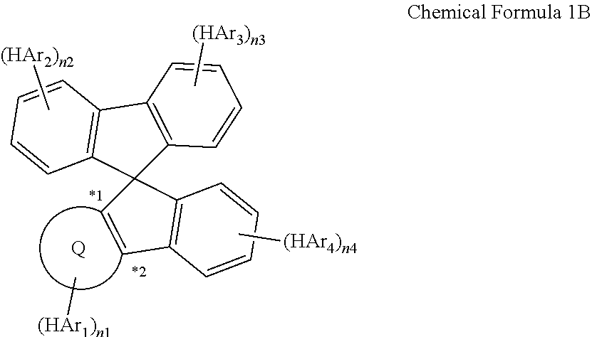


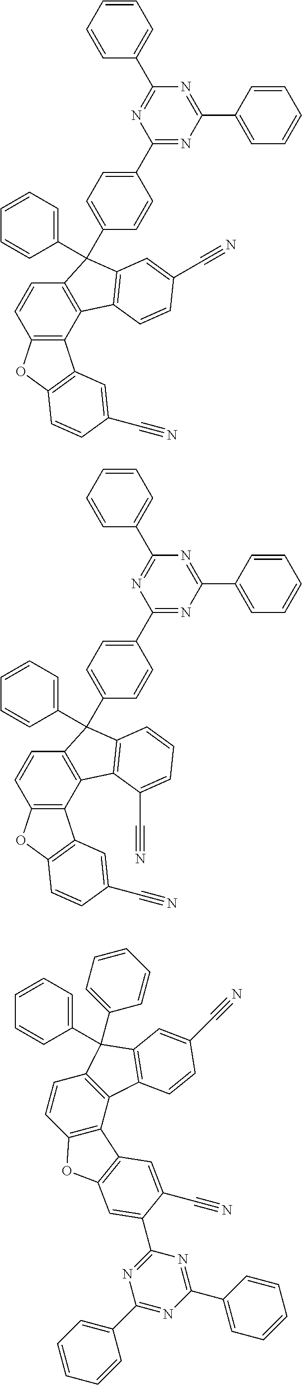


| TABLE 1 | |||||
| Voltage | |||||
| Compound | (V | Efficiency | |||
| (Electron | @20 | (cd/A | |||
| transport | mA/ | @20 | Color index | T95 | |
| layer) | cm2) | mA/cm2) | (x, y) | (hr) | |
| Example 1-1 | Compound 1 | 4.18 | 6.24 | (0.141, 0.046) | 275 |
| Example 1-2 | Compound 2 | 4.26 | 6.21 | (0.142, 0.045) | 255 |
| Example 1-3 | Compound 3 | 4.78 | 6.58 | (0.143, 0.047) | 244 |
| Example 1-4 | Compound 4 | 4.24 | 6.91 | (0.143, 0.046) | 254 |
| Example 1-5 | Compound 5 | 4.12 | 6.54 | (0.144, 0.044) | 270 |
| Example 1-6 | Compound 6 | 4.11 | 6.43 | (0.141, 0.047) | 234 |
| Example 1-7 | Compound 9 | 4.42 | 6.45 | (0.142, 0.046) | 221 |
| Example 1-8 | Compound 10 | 4.31 | 6.12 | (0.141, 0.047) | 236 |
| Example 1-9 | Compound 11 | 4.29 | 6.27 | (0.141, 0.046) | 242 |
| Comparative | Compound ET1 | 4.43 | 5.66 | (0.145, 0.049) | 194 |
| Example 1-1 | |||||
| Comparative | Compound ET2 | 4.98 | 5.42 | (0.148, 0.051) | 142 |
| Example 1-2 | |||||
| Comparative | Compound ET3 | 5.53 | 5.19 | (0.146, 0.053) | 98 |
| Example 1-3 | |||||
| Comparative | Compound ET4 | 4.69 | 5.74 | (0.146, 0.052) | 167 |
| Example 1-4 | |||||
| Comparative | Compound ET5 | 4.92 | 5.89 | (0.145, 0.050) | 159 |
| Example 1-5 | |||||
| Comparative | Compound ET6 | 5.11 | 6.11 | (0.145, 0.052) | 117 |
| Example 1-6 | |||||
| Comparative | Compound ET7 | 4.58 | 5.61 | (0.146, 0.051) | 148 |
| Example 1-7 | |||||
-
- 1: substrate
- 2: anode
- 3: hole transport layer
- 4: light emitting layer
- 5: electron transport layer
- 6: cathode
- 7: hole injection layer
- 8: electron blocking layer
- 9: hole blocking layer
- 10: electron injection layer
Claims (16)


Applications Claiming Priority (5)
| Application Number | Priority Date | Filing Date | Title |
|---|---|---|---|
| KR20180146587 | 2018-11-23 | ||
| KR10-2018-0146587 | 2018-11-23 | ||
| KR10-2019-0150704 | 2019-11-21 | ||
| KR1020190150704A KR102341241B1 (en) | 2018-11-23 | 2019-11-21 | Novel compound and organic light emitting device comprising the same |
| PCT/KR2019/016170 WO2020106108A1 (en) | 2018-11-23 | 2019-11-22 | Novel compound and organic light emitting device using same |
Publications (2)
| Publication Number | Publication Date |
|---|---|
| US20210313518A1 US20210313518A1 (en) | 2021-10-07 |
| US11980090B2 true US11980090B2 (en) | 2024-05-07 |
Family
ID=71090842
Family Applications (1)
| Application Number | Title | Priority Date | Filing Date |
|---|---|---|---|
| US17/262,114 Active 2041-08-10 US11980090B2 (en) | 2018-11-23 | 2019-11-22 | Compound and organic light emitting device comprising the same |
Country Status (3)
| Country | Link |
|---|---|
| US (1) | US11980090B2 (en) |
| KR (1) | KR102341241B1 (en) |
| CN (1) | CN112424190B (en) |
Families Citing this family (1)
| Publication number | Priority date | Publication date | Assignee | Title |
|---|---|---|---|---|
| CN117343078A (en) | 2021-11-25 | 2024-01-05 | 北京夏禾科技有限公司 | Organic electroluminescent material and device |
Citations (21)
| Publication number | Priority date | Publication date | Assignee | Title |
|---|---|---|---|---|
| KR20000051826A (en) | 1999-01-27 | 2000-08-16 | 성재갑 | New organomattalic complex molecule for the fabrication of organic light emitting diodes |
| WO2003012890A2 (en) | 2001-07-20 | 2003-02-13 | Novaled Gmbh | Light emitting component with organic layers |
| WO2013017189A1 (en) | 2011-07-29 | 2013-02-07 | Merck Patent Gmbh | Compounds for electronic devices |
| KR101429035B1 (en) | 2013-05-16 | 2014-08-12 | 롬엔드하스전자재료코리아유한회사 | Organic Electroluminescent Compounds and Organic Electroluminescent Device Comprising the Same |
| CN104066739A (en) | 2011-12-01 | 2014-09-24 | 罗门哈斯电子材料韩国有限公司 | Novel organic electroluminescent compounds and organic electroluminescent device using the same |
| WO2014200148A1 (en) | 2013-06-13 | 2014-12-18 | 제일모직 주식회사 | Organic compound, organic optoelectronic device and display device |
| CN105481811A (en) * | 2015-12-18 | 2016-04-13 | 上海道亦化工科技有限公司 | Compound with screw structure and organic electroluminescent device thereof |
| CN105899501A (en) | 2014-01-09 | 2016-08-24 | 三星Sdi株式会社 | Organic compound, organic optoelectronic device, and display device |
| KR20160134571A (en) | 2015-05-14 | 2016-11-23 | 주식회사 엘지화학 | Hetero-cyclic compound and organic light emitting device comprising the same |
| US20170207397A1 (en) * | 2016-01-18 | 2017-07-20 | Sfc Co., Ltd. | Organic light emitting compounds and organic light emitting devices including the same |
| CN107108578A (en) | 2015-01-30 | 2017-08-29 | 默克专利有限公司 | The material of electronic device |
| WO2017146522A1 (en) | 2016-02-25 | 2017-08-31 | 주식회사 엘지화학 | Heterocyclic compound and organic light emitting diode containing same |
| CN107325036A (en) * | 2017-07-13 | 2017-11-07 | 长春海谱润斯科技有限公司 | A kind of electroluminescent organic material and its organic luminescent device |
| US20180040834A1 (en) * | 2016-07-27 | 2018-02-08 | Sfc Co., Ltd. | Organic light emitting compound and organic light emitting diode including the same |
| KR20180060619A (en) | 2016-11-29 | 2018-06-07 | 에스에프씨 주식회사 | Novel heterocyclic compounds and organic light-emitting diode including the same |
| KR20180086126A (en) * | 2017-01-20 | 2018-07-30 | 주식회사 엘지화학 | Novel hetero-cyclic compound and organic light emitting device comprising the same |
| KR20190010500A (en) | 2017-07-20 | 2019-01-30 | 주식회사 엘지화학 | Novel hetero-cyclic compound and organic light emitting device comprising the same |
| EP3503240A1 (en) * | 2017-12-21 | 2019-06-26 | Novaled GmbH | Organic semiconductor layer |
| US10873035B2 (en) * | 2016-02-23 | 2020-12-22 | Lg Chem, Ltd. | Heterocyclic compound and organic light emitting diode containing same |
| US20210280794A1 (en) * | 2018-11-13 | 2021-09-09 | Lg Chem, Ltd. | Novel compound and organic light emitting device comprising the same |
| US11121329B2 (en) * | 2017-11-24 | 2021-09-14 | Samsung Display Co., Ltd. | Amine compound and organic electroluminescence device including the same |
-
2019
- 2019-11-21 KR KR1020190150704A patent/KR102341241B1/en active IP Right Grant
- 2019-11-22 US US17/262,114 patent/US11980090B2/en active Active
- 2019-11-22 CN CN201980047227.2A patent/CN112424190B/en active Active
Patent Citations (37)
| Publication number | Priority date | Publication date | Assignee | Title |
|---|---|---|---|---|
| KR20000051826A (en) | 1999-01-27 | 2000-08-16 | 성재갑 | New organomattalic complex molecule for the fabrication of organic light emitting diodes |
| WO2003012890A2 (en) | 2001-07-20 | 2003-02-13 | Novaled Gmbh | Light emitting component with organic layers |
| US20040251816A1 (en) | 2001-07-20 | 2004-12-16 | Karl Leo | Light emitting component with organic layers |
| US20140225040A1 (en) | 2011-07-29 | 2014-08-14 | Merck Patent Gmbh Patents & Scientific Information | Compounds for electronic devices |
| WO2013017189A1 (en) | 2011-07-29 | 2013-02-07 | Merck Patent Gmbh | Compounds for electronic devices |
| CN104066739A (en) | 2011-12-01 | 2014-09-24 | 罗门哈斯电子材料韩国有限公司 | Novel organic electroluminescent compounds and organic electroluminescent device using the same |
| US20140357866A1 (en) | 2011-12-01 | 2014-12-04 | Rohm And Haas Electronic Materials Korea Ltd. | Novel organic electroluminescent compounds and organic electroluminescent device using the same |
| KR101429035B1 (en) | 2013-05-16 | 2014-08-12 | 롬엔드하스전자재료코리아유한회사 | Organic Electroluminescent Compounds and Organic Electroluminescent Device Comprising the Same |
| WO2014185751A1 (en) | 2013-05-16 | 2014-11-20 | Rohm And Haas Electronic Materials Korea Ltd. | Organic electroluminescent compounds and organic electroluminescent device comprising the same |
| KR20140145456A (en) | 2013-06-13 | 2014-12-23 | 제일모직주식회사 | Organic compound and organic optoelectric device and display device |
| US20150349270A1 (en) | 2013-06-13 | 2015-12-03 | Samsung Sdi Co., Ltd. | Organic compound, organic optoelectronic device and display device |
| WO2014200148A1 (en) | 2013-06-13 | 2014-12-18 | 제일모직 주식회사 | Organic compound, organic optoelectronic device and display device |
| CN105899501A (en) | 2014-01-09 | 2016-08-24 | 三星Sdi株式会社 | Organic compound, organic optoelectronic device, and display device |
| US20160329506A1 (en) | 2014-01-09 | 2016-11-10 | Samsung Sdi Co., Ltd. | Organic compound, organic optoelectronic device, and display device |
| US20180006237A1 (en) | 2015-01-30 | 2018-01-04 | Merck Patent Gmbh | Materials for electronic devices |
| CN107108578A (en) | 2015-01-30 | 2017-08-29 | 默克专利有限公司 | The material of electronic device |
| KR20170110641A (en) | 2015-01-30 | 2017-10-11 | 메르크 파텐트 게엠베하 | Materials for electronic devices |
| KR20160134571A (en) | 2015-05-14 | 2016-11-23 | 주식회사 엘지화학 | Hetero-cyclic compound and organic light emitting device comprising the same |
| US20180127385A1 (en) | 2015-05-14 | 2018-05-10 | Lg Chem Ltd. | Heterocyclic compound and organic light emitting device comprising same |
| CN107635973A (en) | 2015-05-14 | 2018-01-26 | 株式会社Lg化学 | Heterocyclic compound and the organic luminescent device for including it |
| US10745362B2 (en) * | 2015-05-14 | 2020-08-18 | Lg Chem, Ltd. | Heterocyclic compound and organic light emitting device comprising same |
| CN105481811A (en) * | 2015-12-18 | 2016-04-13 | 上海道亦化工科技有限公司 | Compound with screw structure and organic electroluminescent device thereof |
| US20170207397A1 (en) * | 2016-01-18 | 2017-07-20 | Sfc Co., Ltd. | Organic light emitting compounds and organic light emitting devices including the same |
| US10873035B2 (en) * | 2016-02-23 | 2020-12-22 | Lg Chem, Ltd. | Heterocyclic compound and organic light emitting diode containing same |
| WO2017146522A1 (en) | 2016-02-25 | 2017-08-31 | 주식회사 엘지화학 | Heterocyclic compound and organic light emitting diode containing same |
| US20200123138A1 (en) | 2016-02-25 | 2020-04-23 | Lg Chem, Ltd. | Heterocyclic compound and organic light emitting diode containing same |
| US10822330B2 (en) * | 2016-02-25 | 2020-11-03 | Lg Chem, Ltd. | Heterocyclic compound and organic light emitting diode containing same |
| KR20170100452A (en) | 2016-02-25 | 2017-09-04 | 주식회사 엘지화학 | Hetero-cyclic compound and organic light emitting device comprising the same |
| US20180040834A1 (en) * | 2016-07-27 | 2018-02-08 | Sfc Co., Ltd. | Organic light emitting compound and organic light emitting diode including the same |
| KR20180060619A (en) | 2016-11-29 | 2018-06-07 | 에스에프씨 주식회사 | Novel heterocyclic compounds and organic light-emitting diode including the same |
| KR20180086126A (en) * | 2017-01-20 | 2018-07-30 | 주식회사 엘지화학 | Novel hetero-cyclic compound and organic light emitting device comprising the same |
| CN107325036A (en) * | 2017-07-13 | 2017-11-07 | 长春海谱润斯科技有限公司 | A kind of electroluminescent organic material and its organic luminescent device |
| KR20190010500A (en) | 2017-07-20 | 2019-01-30 | 주식회사 엘지화학 | Novel hetero-cyclic compound and organic light emitting device comprising the same |
| KR102136381B1 (en) | 2017-07-20 | 2020-07-21 | 주식회사 엘지화학 | Novel hetero-cyclic compound and organic light emitting device comprising the same |
| US11121329B2 (en) * | 2017-11-24 | 2021-09-14 | Samsung Display Co., Ltd. | Amine compound and organic electroluminescence device including the same |
| EP3503240A1 (en) * | 2017-12-21 | 2019-06-26 | Novaled GmbH | Organic semiconductor layer |
| US20210280794A1 (en) * | 2018-11-13 | 2021-09-09 | Lg Chem, Ltd. | Novel compound and organic light emitting device comprising the same |
Non-Patent Citations (3)
| Title |
|---|
| Machine translation of CN 105481811 (no date). * |
| Machine translation of KR 2018-0060619 (no date). * |
| Translation of WO written opinion (no date). * |
Also Published As
| Publication number | Publication date |
|---|---|
| CN112424190B (en) | 2023-12-22 |
| KR20200061300A (en) | 2020-06-02 |
| CN112424190A (en) | 2021-02-26 |
| KR102341241B1 (en) | 2021-12-20 |
| US20210313518A1 (en) | 2021-10-07 |
Similar Documents
| Publication | Publication Date | Title |
|---|---|---|
| US12060372B2 (en) | Compound and organic light emitting device comprising the same | |
| US11594685B2 (en) | Organic light emitting device | |
| US20220006022A1 (en) | Compound and organic light emitting device comprising same | |
| US20220384729A1 (en) | Organic light emitting device | |
| US11997925B2 (en) | Cyclic compound and organic light emitting device comprising same | |
| US20210130295A1 (en) | Compound and organic light emitting device comprising the same | |
| US20220259208A1 (en) | Organic light emitting device | |
| US11910711B2 (en) | Cyclic compound and organic light emitting device comprising same | |
| US11542258B2 (en) | Heterocyclic compound and organic light emitting device comprising the same | |
| US20210230182A1 (en) | Novel compound and organic light emitting device comprising the same | |
| US20230240140A1 (en) | Organic light emitting device | |
| US12058931B2 (en) | Heterocyclic compound and organic light emitting device comprising same | |
| US11453650B2 (en) | Heterocyclic compound and organic light emitting device comprising the same | |
| US11925113B2 (en) | Heterocyclic compound and organic light emitting device comprising the same | |
| US20230200229A1 (en) | Organic light emitting device | |
| US20210280794A1 (en) | Novel compound and organic light emitting device comprising the same | |
| US11787818B2 (en) | Compound and organic light emitting device comprising the same | |
| US20210323948A1 (en) | Novel compound and organic light emitting device comprising the same | |
| US12022730B2 (en) | Compound and organic light emitting device comprising the same | |
| US12010912B2 (en) | Heterocyclic compound and organic light emitting device comprising the same | |
| US20240294515A1 (en) | Novel compound and organic light emitting device comprising the same | |
| US20240206332A1 (en) | Organic light emitting device | |
| US20240122068A1 (en) | Organic light emitting device | |
| US11980090B2 (en) | Compound and organic light emitting device comprising the same | |
| US11832517B2 (en) | Heterocyclic compound and organic light emitting device comprising same |
Legal Events
| Date | Code | Title | Description |
|---|---|---|---|
| AS | Assignment |
Owner name: LG CHEM, LTD., KOREA, REPUBLIC OF Free format text: ASSIGNMENT OF ASSIGNORS INTEREST;ASSIGNORS:LEE, JAE TAK;HONG, SUNG KIL;HUH, JUNGOH;AND OTHERS;REEL/FRAME:054989/0127 Effective date: 20201202 |
|
| FEPP | Fee payment procedure |
Free format text: ENTITY STATUS SET TO UNDISCOUNTED (ORIGINAL EVENT CODE: BIG.); ENTITY STATUS OF PATENT OWNER: LARGE ENTITY |
|
| STPP | Information on status: patent application and granting procedure in general |
Free format text: DOCKETED NEW CASE - READY FOR EXAMINATION |
|
| STPP | Information on status: patent application and granting procedure in general |
Free format text: NON FINAL ACTION MAILED |
|
| STPP | Information on status: patent application and granting procedure in general |
Free format text: RESPONSE TO NON-FINAL OFFICE ACTION ENTERED AND FORWARDED TO EXAMINER |
|
| STPP | Information on status: patent application and granting procedure in general |
Free format text: NOTICE OF ALLOWANCE MAILED -- APPLICATION RECEIVED IN OFFICE OF PUBLICATIONS |
|
| ZAAB | Notice of allowance mailed |
Free format text: ORIGINAL CODE: MN/=. |
|
| STPP | Information on status: patent application and granting procedure in general |
Free format text: PUBLICATIONS -- ISSUE FEE PAYMENT VERIFIED |
|
| STCF | Information on status: patent grant |
Free format text: PATENTED CASE |
|
| CC | Certificate of correction |