EP3503191B1 - Cmos image sensor encapsulation structure and method for manufacturing the same - Google Patents
Cmos image sensor encapsulation structure and method for manufacturing the same Download PDFInfo
- Publication number
- EP3503191B1 EP3503191B1 EP18207491.4A EP18207491A EP3503191B1 EP 3503191 B1 EP3503191 B1 EP 3503191B1 EP 18207491 A EP18207491 A EP 18207491A EP 3503191 B1 EP3503191 B1 EP 3503191B1
- Authority
- EP
- European Patent Office
- Prior art keywords
- wafer
- insulating layer
- image sensor
- transparent substrate
- cmos image
- Prior art date
- Legal status (The legal status is an assumption and is not a legal conclusion. Google has not performed a legal analysis and makes no representation as to the accuracy of the status listed.)
- Active
Links
Images


Classifications
-
- H—ELECTRICITY
- H10—SEMICONDUCTOR DEVICES; ELECTRIC SOLID-STATE DEVICES NOT OTHERWISE PROVIDED FOR
- H10F—INORGANIC SEMICONDUCTOR DEVICES SENSITIVE TO INFRARED RADIATION, LIGHT, ELECTROMAGNETIC RADIATION OF SHORTER WAVELENGTH OR CORPUSCULAR RADIATION
- H10F39/00—Integrated devices, or assemblies of multiple devices, comprising at least one element covered by group H10F30/00, e.g. radiation detectors comprising photodiode arrays
- H10F39/80—Constructional details of image sensors
- H10F39/804—Containers or encapsulations
-
- H—ELECTRICITY
- H10—SEMICONDUCTOR DEVICES; ELECTRIC SOLID-STATE DEVICES NOT OTHERWISE PROVIDED FOR
- H10F—INORGANIC SEMICONDUCTOR DEVICES SENSITIVE TO INFRARED RADIATION, LIGHT, ELECTROMAGNETIC RADIATION OF SHORTER WAVELENGTH OR CORPUSCULAR RADIATION
- H10F39/00—Integrated devices, or assemblies of multiple devices, comprising at least one element covered by group H10F30/00, e.g. radiation detectors comprising photodiode arrays
- H10F39/011—Manufacture or treatment of image sensors covered by group H10F39/12
- H10F39/014—Manufacture or treatment of image sensors covered by group H10F39/12 of CMOS image sensors
-
- H—ELECTRICITY
- H10—SEMICONDUCTOR DEVICES; ELECTRIC SOLID-STATE DEVICES NOT OTHERWISE PROVIDED FOR
- H10F—INORGANIC SEMICONDUCTOR DEVICES SENSITIVE TO INFRARED RADIATION, LIGHT, ELECTROMAGNETIC RADIATION OF SHORTER WAVELENGTH OR CORPUSCULAR RADIATION
- H10F39/00—Integrated devices, or assemblies of multiple devices, comprising at least one element covered by group H10F30/00, e.g. radiation detectors comprising photodiode arrays
- H10F39/011—Manufacture or treatment of image sensors covered by group H10F39/12
- H10F39/018—Manufacture or treatment of image sensors covered by group H10F39/12 of hybrid image sensors
-
- H—ELECTRICITY
- H10—SEMICONDUCTOR DEVICES; ELECTRIC SOLID-STATE DEVICES NOT OTHERWISE PROVIDED FOR
- H10F—INORGANIC SEMICONDUCTOR DEVICES SENSITIVE TO INFRARED RADIATION, LIGHT, ELECTROMAGNETIC RADIATION OF SHORTER WAVELENGTH OR CORPUSCULAR RADIATION
- H10F39/00—Integrated devices, or assemblies of multiple devices, comprising at least one element covered by group H10F30/00, e.g. radiation detectors comprising photodiode arrays
- H10F39/011—Manufacture or treatment of image sensors covered by group H10F39/12
- H10F39/026—Wafer-level processing
-
- H—ELECTRICITY
- H10—SEMICONDUCTOR DEVICES; ELECTRIC SOLID-STATE DEVICES NOT OTHERWISE PROVIDED FOR
- H10F—INORGANIC SEMICONDUCTOR DEVICES SENSITIVE TO INFRARED RADIATION, LIGHT, ELECTROMAGNETIC RADIATION OF SHORTER WAVELENGTH OR CORPUSCULAR RADIATION
- H10F39/00—Integrated devices, or assemblies of multiple devices, comprising at least one element covered by group H10F30/00, e.g. radiation detectors comprising photodiode arrays
- H10F39/10—Integrated devices
- H10F39/12—Image sensors
- H10F39/18—Complementary metal-oxide-semiconductor [CMOS] image sensors; Photodiode array image sensors
-
- H—ELECTRICITY
- H10—SEMICONDUCTOR DEVICES; ELECTRIC SOLID-STATE DEVICES NOT OTHERWISE PROVIDED FOR
- H10F—INORGANIC SEMICONDUCTOR DEVICES SENSITIVE TO INFRARED RADIATION, LIGHT, ELECTROMAGNETIC RADIATION OF SHORTER WAVELENGTH OR CORPUSCULAR RADIATION
- H10F39/00—Integrated devices, or assemblies of multiple devices, comprising at least one element covered by group H10F30/00, e.g. radiation detectors comprising photodiode arrays
- H10F39/80—Constructional details of image sensors
- H10F39/806—Optical elements or arrangements associated with the image sensors
- H10F39/8063—Microlenses
-
- H—ELECTRICITY
- H10—SEMICONDUCTOR DEVICES; ELECTRIC SOLID-STATE DEVICES NOT OTHERWISE PROVIDED FOR
- H10W—GENERIC PACKAGES, INTERCONNECTIONS, CONNECTORS OR OTHER CONSTRUCTIONAL DETAILS OF DEVICES COVERED BY CLASS H10
- H10W72/00—Interconnections or connectors in packages
- H10W72/20—Bump connectors, e.g. solder bumps or copper pillars; Dummy bumps; Thermal bumps
Definitions
- the present disclosure relates to the technical field of image sensors, and particularly to a CMOS image sensor encapsulation structure and a method for manufacturing the same.
- CMOS abbreviation of Complementary Metal-Oxide Semiconductor
- image sensor is usually a core part of digital cameras.
- Document CN 103 000 649 discloses a method of manufacturing a CMOS image sensor encapsulation structure involving wafer thinning.
- An object of the present disclosure is to provide a method for manufacturing a CMOS image sensor encapsulation structure, by which a CMOS image sensor encapsulation structure having a relatively small thickness can be manufactured.
- the other object of the present disclosure is to provide a CMOS image sensor encapsulation structure which is featured by having a small thickness.
- a method for manufacturing a CMOS image sensor encapsulation structure comprising:
- the wafer before being thinned by grinding has a thickness of 700 ⁇ 1000 ⁇ m
- the wafer after being thinned by grinding has a thickness of 20 ⁇ 100 ⁇ m
- the wafer after being thinned by grinding has a thickness of 40 ⁇ 70 ⁇ m.
- the electrically conductive material includes copper.
- the transparent substrate material is fixed to the surface of the first insulating layer by a light-transmissive adhesive glue.
- materials of the transparent substrate material include sapphire, quartz glass and magnesium oxide.
- areas where the micro convex lens and the blind hole are located are a first installation area and a second installation area, respectively, the first installation area and the second installation area do not overlap each other, and the transparent substrate material is provided in the first installation area.
- the transparent substrate material covers a whole surface of the combined layer.
- the method further includes: forming a third insulating layer on a surface of the wafer that is thinned by grinding such that the electrically conductive material is exposed, then forming metal projections on the third insulating layer and electrically connecting the metal projections to the electrically conductive material.
- CMOS image sensor encapsulation structure including:
- the transparent substrate material covers a whole surface of the combined layer.
- the CMOS image sensor encapsulation structure further includes: a dummy wafer formed on a side of the first insulating layer, with the side away from the wafer, wherein the dummy wafer is fixed to the transparent substrate material.
- the dummy wafer is bond-fixed on a surface of the transparent substrate material by an adhesive glue, wherein a gap between the second installation area and the dummy wafer is filled up with the adhesive glue, such that the dummy wafer covers a surface of the whole combined layer.
- the CMOS image sensor encapsulation structure further includes: a third insulating layer formed on a surface of a side of the wafer, with the side away from the first insulating layer.
- the CMOS image sensor encapsulation structure further includes: a plurality of metal projections formed on a side of the wafer, with the side away from the first insulating layer, wherein two metal projections among the plurality of metal projections pass through the third insulating layer to be electrically connected to the electrically conductive material.
- the CMOS image sensor encapsulation structure further includes: solder balls formed on a side of the metal projections away from the wafer.
- the wafer has a thickness of 20 ⁇ 100 ⁇ m.
- the present disclosure has the following beneficial effects: with the method for manufacturing a CMOS image sensor encapsulation structure provided in the examples of the present disclosure, in the process of manufacturing the CMOS image sensor encapsulation structure, firstly, the transparent substrate material is fixed to the surface of the first insulating layer, with the surface having the micro convex lens, the dummy wafer is fixed on the surface of the transparent substrate material, and then the wafer is thinned by grinding, and in this process, the transparent substrate material provides more mechanical support force for the wafer, therefore, the wafer can become thinner by grinding, thus the CMOS image sensor encapsulation structure is characterized in that the structure is formed in a thin shape. Moreover, in the manufacture process, the transparent substrate material is manufactured in a semiconductor factory, thus the cleanliness is higher, and pollution to the CMOS image sensor encapsulation structure can be avoided.
- orientational or positional relations indicated by terms “thickness”, “upper”, “lower”, and so on are based on orientational or positional relations as shown in the accompanying drawings, merely for facilitating describing the present disclosure and simplifying the description, rather than indicating or implying that related devices or elements have to be in the specific orientation or configured and operated in the specific orientation, and therefore, they should not be construed as limiting the present disclosure.
- first”, “second”, and “third” are merely for descriptive purpose, and should not be construed as indicating or implying relative importance or implicitly indicating the number of a related technical feature. Thus, for a feature defined with “first”, “second”, or “third”, it may explicitly or implicitly indicate that one or more such features are included.
- connection can be a fixed connection, a detachable connection, or an integrated connection; it can be a direct connection, an indirect connection via an intermediate medium, or an internal communication between two elements or an interaction relation between two elements.
- the examples of the present disclosure provide a method for manufacturing a CMOS image sensor encapsulation structure 100.
- the CMOS image sensor encapsulation structure 100 manufactured by this method is characterized in that the structure is formed in a thin shape, referring to FIG. 1 .
- a transparent substrate material 160 is manufactured in a semiconductor factory, thus the cleanliness is higher, and pollution to the CMOS image sensor encapsulation structure 100 can be avoided.
- the method for manufacturing a CMOS image sensor encapsulation structure 100 includes the following steps:
- a position of the IC (internal elements and circuits) in the combined layer should be located above a bottom portion of the blind hole 130, in this way, damage to the IC in the combined layer can be avoided when the wafer 110 is thinned by grinding in a subsequent procedure.
- the second insulating layer 150 is formed on the hole wall of the blind hole 130 by deposition. Besides, in a process of being formed on the hole wall of the blind hole 130, the second insulating layer 150 also may be formed on the hole bottom of the blind hole 130, but the second insulating layer 150 formed on the hole bottom of the blind hole 130 finally will be ground off. Therefore, it is just needed to ensure that the second insulating layer 150 is formed on the hole wall of the blind hole 130.
- the electrically conductive material 151 includes copper.
- the electrically conductive material 151 also can be silver, gold, aluminum, and so on. As copper is relatively cheap, and has relatively good electrical conductivity, copper is selected as the electrically conductive material 151 in the present example.
- the transparent substrate material 160 is fixed on a surface of the first insulating layer 120, with the surface having the micro convex lens 140, a dummy wafer 170 is fixed on a surface of the transparent substrate material 160, and then the wafer 110 is thinned by grinding such that the electrically conductive material 151 in the blind hole 130 is exposed.
- the transparent substrate material 160 is fixed on the surface of the first insulating layer 120, with the surface having the micro convex lens 140, and the transparent substrate material 160 can transmit light into the micro convex lens 140.
- the dummy wafer 170 is used to connect a CMP (Chemical Mechanical Polishing) grinding head, and the CMP grinding head is used to perform a process of thinning the wafer 110 by grinding. Since the transparent substrate material 160 can provide more mechanical support for the combined layer, when the wafer 110 is thinned by grinding, the wafer 110 can become thinner by grinding.
- CMP Chemical Mechanical Polishing
- the wafer 110 before being thinned by grinding has a thickness of 700 ⁇ 1000 ⁇ m
- the wafer 110 after being thinned by grinding has a thickness of 20 ⁇ 100 ⁇ m
- the wafer 110 after being thinned by grinding has a thickness of 40 ⁇ 70 ⁇ m.
- materials of the transparent substrate material 160 include sapphire, quartz glass and magnesium oxide. All of these materials are featured by relatively good light transmittance, and then by using them as the transparent substrate material 160, light can better pass through the transparent substrate material 160 to be received by the micro convex lens 140.
- the transparent substrate material 160 is fixed to the surface of the first insulating layer 120 by a light-transmissive adhesive glue.
- the light-transmissive adhesive glue is a high-light-transmittance adhesive glue 161.
- the high-light-transmittance adhesive glue 161 not only can ensure reliability of connection of the transparent substrate material 160 to the first insulating layer 120 and to the micro convex lens 140, but also will not hinder light from passing through the transparent substrate material 160 to enter the micro convex lens 140.
- the high-light-transmittance adhesive glue 161 can contact a whole surface of the transparent substrate material 160, that is, a gap between the transparent substrate material 160 and the first insulating layer 120 is filled up with the high-light-transmittance adhesive glue 161, in this way, it can be ensured that there are more contact points between the transparent substrate material 160 and the combined layer, thus a sufficient support force can be provided when the wafer 110 is thinned by grinding.
- areas where the micro convex lens 140 and the blind hole 130 are located are a first installation area 171 and a second installation area 172, respectively.
- the first installation area 171 and the second installation area 172 do not overlap each other.
- the transparent substrate material 160 is provided in the first installation area 171.
- the first installation area 171 is located in a middle region of the combined layer, and the second installation area 172 is located in an edge region of the combined layer. Such arrangement benefits subsequent cutting.
- the dummy wafer 170 is bonded by an adhesive glue, so as to be fixed on the surface of the transparent substrate material 160.
- the second installation area 172 is also filled with the adhesive glue, such that the dummy wafer 170 covers the whole combined layer.
- the transparent substrate material 160 covers the whole surface of the combined layer.
- the third insulating layer 173 in a region corresponding to the electrically conductive material 151 is removed such that the electrically conductive material 151 is exposed, then a part of the metal projections 174 are formed at the electrically conductive material 151 and electrically connected to the electrically conductive material 151, and the other part of metal projections 174 are formed on a surface of the third insulating layer 173 and electrically connected to the metal projections 174 formed at the electrically conductive material 151, such that the metal projections 174 on the third insulating layer 173 are electrically connected to the electrically conductive material 151.
- a circuit in the IC (internal elements and circuits) can be guided out to the metal projections 174.
- the solder balls 175 are welded on the metal projections 174.
- An electrical signal of a chip can be connected to a system base board via the solder balls 175.
- the first insulating layer 120, the second insulating layer 150, and the third insulating layer 173 can be SiO 2 , Si 3 N 4 , BPGS (BSG borosilicate glass, borophosphate glass), an organic resin or a mixture of organic resin and inorganic resin.
- BPGS BSG borosilicate glass, borophosphate glass
- the transparent substrate material 160 is fixed to the surface of the first insulating layer 120, with the surface having the micro convex lens 140, the dummy wafer 170 is formed on the surface of the transparent substrate material 160, and then the wafer 110 is thinned by grinding, and in this process, the transparent substrate material 160 provides more mechanical support force for the wafer 110, therefore, the wafer 110 can become thinner by grinding, thus the CMOS image sensor encapsulation structure 100 is characterized in that the structure is formed in a thin shape. Moreover, in the manufacture process, the transparent substrate material 160 is manufactured in a semiconductor factory, thus the cleanliness is higher, and pollution to the CMOS image sensor encapsulation structure 100 can be avoided.
- the example of the present disclosure further provide a CMOS image sensor encapsulation structure 100, again as shown in FIG.1 , including a wafer 110, a first insulating layer 120, a micro convex lens 140, a transparent substrate material 160, a high-light-transmittance adhesive glue 161, an internal IC circuit, and an electrically conductive material 151.
- a CMOS image sensor encapsulation structure 100 again as shown in FIG.1 , including a wafer 110, a first insulating layer 120, a micro convex lens 140, a transparent substrate material 160, a high-light-transmittance adhesive glue 161, an internal IC circuit, and an electrically conductive material 151.
- a material and a dimension of the wafer 110 can be determined according to practical requirements.
- the first insulating layer 120 is formed on a side of the wafer 110, and the first insulating layer 120 and the wafer 110 form a combined layer.
- a material of the first insulating layer 120 can be one or more selected from the group consisting of SiO 2 , Si 3 N 4 , BPGS (BSG borosilicate glass, borophosphate glass), an organic resin and a mixture of organic resin and inorganic resin.
- the specific material of the first insulating layer 120 is not limited in the present disclosure.
- the micro convex lens 140 is formed in the combined layer.
- a region in the combined layer where the micro convex lens 140 is formed forms a first installation area 171.
- a region in the combined layer other than the first installation area 171 is a second installation area 172.
- the number of the micro convex lens 140 can be in plurality.
- a plurality of micro convex lenses 140 form a lens array.
- the micro convex lens 140 can converge light and then transmit the light into the internal IC circuit.
- the transparent substrate material 160 is formed on a side of the first insulating layer 120, with the side away from the wafer 110, wherein the transparent substrate material 160 at least covers the first installation area 171.
- the transparent substrate material 160 is fixed on surfaces of the first insulating layer 120 and the micro convex lens 140 by a high-light-transmittance adhesive glue 161.
- a gap between the transparent substrate material 160 and the first insulating layer 120 is filled up with the high-light-transmittance adhesive glue 161.
- the transparent substrate material 160 can merely cover the surface of the micro convex lens 140, and also can cover a whole surface of the combined layer, that is, cover the surfaces of the micro convex lens 140 and the first insulating layer 120.
- Materials of the transparent substrate material 160 can include sapphire, quartz glass and magnesium oxide. All of these materials are featured by relatively good light transmittance, and then external light can better pass through the transparent substrate material 160 to be received by the micro convex lens 140.
- the internal IC circuit is formed in the combined layer.
- the electrically conductive material 151 is formed in the second installation area 172.
- the electrically conductive material 151 passes through the combined layer.
- the electrically conductive material 151 is electrically connected to the internal IC circuit and the micro convex lens 140.
- a second insulating layer 150 is formed between the electrically conductive material 151 and the combined layer.
- the electrically conductive material 151 can be connected to the internal IC circuit via a conductor.
- One end of the electrically conductive material 151 is connected to the internal IC circuit, with the end located at the side of the first insulating layer 120, and the other end is provided on a surface of the wafer 110 away from the first insulating layer 120.
- a detailed method for manufacturing the electrically conductive material 151 can be referred to the above example of method, and it will not be repeated redundantly herein.
- the electrically conductive material 151 can include copper. In other examples, the electrically conductive material 151 also can be silver, gold, aluminum, and so on.
- Materials of the second insulating layer 150 can be one or more selected from the group consisting of SiO 2 , Si 3 N 4 , BPGS (BSG borosilicate glass, borophosphate glass), an organic resin and a mixture of organic resin and inorganic resin. The specific material of the second insulating layer 150 is not limited in the present disclosure.
- this CMOS image sensor encapsulation structure 100 further includes a dummy wafer 170 formed on a side of the first insulating layer 120, with the side away from the wafer 110, wherein the dummy wafer 170 is fixed to the transparent substrate material 160.
- the dummy wafer 170 is used to be connected a CMP grinding head, wherein the CMP grinding head is used to perform a process of thinning the wafer 110 by grinding. Since the transparent substrate material 160 can provide more mechanical support force for the combined layer, when the wafer 110 is thinned by grinding, the wafer 110 can become thinner by grinding.
- the wafer 110 can have a thickness of 20 ⁇ 100 ⁇ m.
- the wafer 110 with such thickness is obtained by grinding the original wafer 110 to make it thinner, after the dummy wafer 170 is already formed.
- the dummy wafer 170 is bond-fixed on a surface of the transparent substrate material 160 by an adhesive glue, wherein a gap between the second installation area 172 and the dummy wafer 170 is filled up with the adhesive glue, such that the dummy wafer 170 covers a surface of the whole combined layer.
- this CMOS image sensor encapsulation structure 100 further includes a third insulating layer 173 formed on a surface of a side of the wafer 110, with the side away from the first insulating layer 120.
- a material of the third insulating layer 173 can be one or more selected from the group consisting of SiO 2 , Si 3 N 4 , BPGS (BSG borosilicate glass, borophosphate glass), an organic resin and a mixture of organic resin and inorganic resin.
- the specific material of the third insulating layer 173 is not limited in the present disclosure.
- this CMOS image sensor encapsulation structure 100 further includes a plurality of metal projections 174 formed on a side of the wafer 110, with the side away from the first insulating layer 120. Two metal projections 174 among the plurality of metal projections 174 pass through the third insulating layer 173 to be electrically connected to the electrically conductive material 151. A part of the metal projections 174 are located on a surface of the third insulating layer 173, and two of the metal projections 174 are directly connected to the electrically conductive material 151.
- this CMOS image sensor encapsulation structure 100 further includes solder balls 175 formed on a side of the metal projections 174, with the side away from the wafer 110. With the solder balls 175, an electrical signal of a chip can be connected to a system base board.
- the transparent substrate material 160 is fixed on the surface of the first insulating layer 120, with the surface having the micro convex lens 140, such that the transparent substrate material 160 can provide a surface for fixing the dummy wafer 170.
- the transparent substrate material 160 can provide more mechanical support force for the wafer 110, such that the wafer 110 can become thinner by grinding, thus the CMOS image sensor encapsulation structure 100 is characterized in that the structure is formed in a thin shape.
- the present disclosure provides a CMOS image sensor encapsulation structure and a method for manufacturing the same.
- the transparent substrate material By fixing the transparent substrate material on the surface of the first insulating layer, with the surface having the micro convex lens, the transparent substrate material can provide a surface for fixing the dummy wafer.
- the transparent substrate material can provide more mechanical support forces for the wafer, such that the wafer can become thinner by grinding, thus the CMOS image sensor encapsulation structure is characterized in that the structure is formed in a thin shape.
Landscapes
- Solid State Image Pick-Up Elements (AREA)
- Structures Or Materials For Encapsulating Or Coating Semiconductor Devices Or Solid State Devices (AREA)
Description
- The present disclosure relates to the technical field of image sensors, and particularly to a CMOS image sensor encapsulation structure and a method for manufacturing the same.
- A CMOS (abbreviation of Complementary Metal-Oxide Semiconductor) sensor, which is a type of image sensor, is usually a core part of digital cameras.
- Currently, conventional CMOS sensors have a problem that their encapsulation structures are relatively thick
- Document
CN 103 000 649 discloses a method of manufacturing a CMOS image sensor encapsulation structure involving wafer thinning. - An object of the present disclosure is to provide a method for manufacturing a CMOS image sensor encapsulation structure, by which a CMOS image sensor encapsulation structure having a relatively small thickness can be manufactured.
- The other object of the present disclosure is to provide a CMOS image sensor encapsulation structure which is featured by having a small thickness.
- The present invention is defined in the independent claims 1 and 9. Preferred embodiments are defined in the dependent claims.
- The present disclosure is implemented as follows.
- A method for manufacturing a CMOS image sensor encapsulation structure, comprising:
- forming a blind hole in a combined layer formed by a first insulating layer and a wafer, wherein the blind hole passes through the first insulating layer with its hole bottom located on the wafer, and a surface of the first insulating layer facing away from the wafer has a micro convex lens; forming a second insulating layer on a hole wall of the blind hole, then filling an electrically conductive material in the blind hole having the second insulating layer, and making a conductor (wire) in the combined layer extend to a surface of the first insulating layer to be electrically connected to the electrically conductive material, with the conductor in signal connection with the micro convex lens and an IC; and
- fixing a transparent substrate material on a surface of the first insulating layer having the micro convex lens, fixing a dummy wafer on a surface of the transparent substrate material, and then thinning the wafer by grinding such that the electrically conductive material in the blind hole is exposed.
- Furthermore, in an example of the present disclosure, the wafer before being thinned by grinding has a thickness of 700∼1000µm, and the wafer after being thinned by grinding has a thickness of 20∼100µm
- Furthermore, in an example of the present disclosure, the wafer after being thinned by grinding has a thickness of 40∼70µm.
- Furthermore, in an example of the present disclosure, the electrically conductive material includes copper.
- Furthermore, in an example of the present disclosure, the transparent substrate material is fixed to the surface of the first insulating layer by a light-transmissive adhesive glue.
- Furthermore, in an example of the present disclosure, materials of the transparent substrate material include sapphire, quartz glass and magnesium oxide.
- Furthermore, in an example of the present disclosure, areas where the micro convex lens and the blind hole are located are a first installation area and a second installation area, respectively, the first installation area and the second installation area do not overlap each other, and the transparent substrate material is provided in the first installation area.
- Furthermore, in an example of the present disclosure, the transparent substrate material covers a whole surface of the combined layer.
- Furthermore, in an example of the present disclosure, after the wafer is thinned by grinding, the method further includes: forming a third insulating layer on a surface of the wafer that is thinned by grinding such that the electrically conductive material is exposed, then forming metal projections on the third insulating layer and electrically connecting the metal projections to the electrically conductive material.
- The present disclosure further provides a CMOS image sensor encapsulation structure, including:
- a wafer;
- a first insulating layer formed on a side of the wafer, wherein the first insulating layer and the wafer form a combined layer;
- a plurality of micro convex lenses formed in the combined layer, a region in the combined layer where the micro convex lenses are formed form a first installation area, and a region in the combined layer other than the first installation area is a second installation area;
- a transparent substrate material formed on a side of the first insulating layer, with the side away from the wafer, wherein the transparent substrate material at least covers the first installation area; the transparent substrate material is fixed on surfaces of the first insulating layer and the micro convex lenses by a high-light-transmittance adhesive glue, and a gap between the transparent substrate material and the first insulating layer is filled up with the high-light-transmittance adhesive glue;
- an internal IC circuit formed in the combined layer, and
- an electrically conductive material formed in the second installation area, wherein the electrically conductive material passes through the combined layer, the electrically conductive material is electrically connected to the internal IC circuit and the micro convex lenses; and a second insulating layer is formed between the electrically conductive material and the combined layer.
- Furthermore, the transparent substrate material covers a whole surface of the combined layer.
- Furthermore, the CMOS image sensor encapsulation structure further includes: a dummy wafer formed on a side of the first insulating layer, with the side away from the wafer, wherein the dummy wafer is fixed to the transparent substrate material.
- Furthermore, the dummy wafer is bond-fixed on a surface of the transparent substrate material by an adhesive glue, wherein a gap between the second installation area and the dummy wafer is filled up with the adhesive glue, such that the dummy wafer covers a surface of the whole combined layer.
- Furthermore, the CMOS image sensor encapsulation structure further includes: a third insulating layer formed on a surface of a side of the wafer, with the side away from the first insulating layer.
- Furthermore, the CMOS image sensor encapsulation structure further includes: a plurality of metal projections formed on a side of the wafer, with the side away from the first insulating layer, wherein two metal projections among the plurality of metal projections pass through the third insulating layer to be electrically connected to the electrically conductive material.
- Furthermore, the CMOS image sensor encapsulation structure further includes: solder balls formed on a side of the metal projections away from the wafer.
- Furthermore, the wafer has a thickness of 20∼100µm.
- The present disclosure has the following beneficial effects: with the method for manufacturing a CMOS image sensor encapsulation structure provided in the examples of the present disclosure, in the process of manufacturing the CMOS image sensor encapsulation structure, firstly, the transparent substrate material is fixed to the surface of the first insulating layer, with the surface having the micro convex lens, the dummy wafer is fixed on the surface of the transparent substrate material, and then the wafer is thinned by grinding, and in this process, the transparent substrate material provides more mechanical support force for the wafer, therefore, the wafer can become thinner by grinding, thus the CMOS image sensor encapsulation structure is characterized in that the structure is formed in a thin shape. Moreover, in the manufacture process, the transparent substrate material is manufactured in a semiconductor factory, thus the cleanliness is higher, and pollution to the CMOS image sensor encapsulation structure can be avoided.
- In order to more clearly illustrate technical solutions of embodiments of the present disclosure, accompanying drawings which are needed for description of the embodiments will be introduced briefly below. It should be understood that the accompanying drawings below merely show some examples of the present disclosure, and therefore should not be considered as limiting the scope. A person ordinarily skilled in the art still can obtain other relevant drawings according to these accompanying drawings, without using inventive effort.
-
FIG. 1 is a schematic structural diagram of a CMOS image sensor encapsulation structure provided in an example of the present disclosure; -
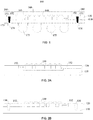
FIG. 2A is a schematic structural diagram of the CMOS image sensor encapsulation structure initially used when Step S1 is carried out in a method for manufacturing a CMOS image sensor encapsulation structure provided in an example of the present disclosure; -
FIG. 2B is a schematic structural diagram after a blind hole is formed in a combined layer when the Step S1 is carried out in the method for manufacturing a CMOS image sensor encapsulation structure provided in the example of the present disclosure; -
FIG. 3A is a schematic structural diagram after an electrically conductive material is filled in the blind hole having a second insulating layer when Step S2 is carried out in the method for manufacturing a CMOS image sensor encapsulation structure provided in the example of the present disclosure; -
FIG. 3B is a schematic structural diagram after a conductor in the combined layer in signal connection with a micro convex lens and an IC to a surface of a first insulating layer and electrically connected to an electrically conductive material when Step S2 is carried out in the method for manufacturing a CMOS image sensor encapsulation structure provided in the example of the present disclosure; -
FIG. 4A is a schematic structural diagram after a transparent substrate material is fixed to a surface of the first insulating layer when Step S3 is carried out in the method for manufacturing a CMOS image sensor encapsulation structure provided in the example of the present disclosure; -
FIG. 4B is a schematic structural diagram after a dummy wafer is fixed to a surface of the transparent substrate material when the Step S3 is carried out in the method for manufacturing a CMOS image sensor encapsulation structure provided in the example of the present disclosure; -
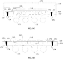
FIG. 4C is a schematic structural diagram after a wafer is thinned by grinding when Step S3 is carried out in the method for manufacturing a CMOS image sensor encapsulation structure provided in the example of the present disclosure; -
FIG. 5A is a schematic structural diagram after a third insulating layer is formed on a surface of the wafer that is thinned by grinding and the electrically conductive material is exposed when Step S4 is carried out in the method for manufacturing a CMOS image sensor encapsulation structure provided in the example of the present disclosure; -
FIG. 5B is a schematic structural diagram after metal projections are formed on the third insulating layer and are electrically connected to the electrically conductive material when the Step S4 is carried out in the method for manufacturing a CMOS image sensor encapsulation structure provided in the example of the present disclosure; -
FIG. 5C is a schematic structural diagram after solder balls are welded on the metal projections when Step S4 is carried out in the method for manufacturing a CMOS image sensor encapsulation structure provided in the example of the present disclosure; -
FIG. 5D is a schematic structural diagram after the dummy wafer is removed when Step S4 is carried out in the method for manufacturing a CMOS image sensor encapsulation structure provided in the example of the present disclosure. - Reference signs: 100-CMOS image sensor encapsulation structure; 110-wafer; 120-first insulation layer; 130-blind hole; 140-micro convex lens; 150-second insulating layer; 151-electrically conductive material; 152-conductor; 160-transparent substrate material; 161-high-light-transmittance adhesive glue; 170-dummy wafer; 171-first installation area; 172-second installation area; 173-third insulating layer; 174-metal projection; 175-solder ball.
- In order to make the objects, technical solutions and advantages of the embodiments of the present disclosure clearer, below the technical solutions in the embodiments of the present disclosure will be described clearly and completely in conjunction with the accompanying drawings in the embodiments of the present disclosure. Apparently, some but not all embodiments of the present disclosure are described. Based on the embodiments of the present disclosure, all the other embodiments, obtained by a person ordinarily skilled in the art without paying inventive effort, should fall within the scope of protection of the present disclosure
- Therefore, the detailed description below of the embodiments of the present disclosure provided in the accompanying drawings is not intended to limit the scope of protection of the present disclosure, but merely represents chosen embodiments of the present disclosure. Based on the embodiments in the present disclosure, all the other embodiments, which a person ordinarily skilled in the art obtains without using inventive effort, fall within the scope of protection of the present disclosure.
- It should be noted that similar reference signs and letters represent similar items in the following accompanying drawings. Therefore, once a certain item is defined in one accompanying drawing, it is not needed to be further defined or explained in subsequent accompanying drawings.
- In the description of the present disclosure, it should be understood that orientational or positional relations indicated by terms "thickness", "upper", "lower", and so on are based on orientational or positional relations as shown in the accompanying drawings, merely for facilitating describing the present disclosure and simplifying the description, rather than indicating or implying that related devices or elements have to be in the specific orientation or configured and operated in the specific orientation, and therefore, they should not be construed as limiting the present disclosure.
- Besides, terms "first", "second", and "third" are merely for descriptive purpose, and should not be construed as indicating or implying relative importance or implicitly indicating the number of a related technical feature. Thus, for a feature defined with "first", "second", or "third", it may explicitly or implicitly indicate that one or more such features are included.
- In the present disclosure, unless otherwise specified and defined explicitly, terms "install", "provide", "fix", and so on should be construed in a broad sense. For example, a connection can be a fixed connection, a detachable connection, or an integrated connection; it can be a direct connection, an indirect connection via an intermediate medium, or an internal communication between two elements or an interaction relation between two elements. For a person ordinarily skilled in the art, specific meanings of the above-mentioned terms in the present disclosure can be understood according to specific circumstances.
- The examples of the present disclosure provide a method for manufacturing a CMOS image
sensor encapsulation structure 100. The CMOS imagesensor encapsulation structure 100 manufactured by this method is characterized in that the structure is formed in a thin shape, referring toFIG. 1 . Moreover, in a manufacture process, atransparent substrate material 160 is manufactured in a semiconductor factory, thus the cleanliness is higher, and pollution to the CMOS imagesensor encapsulation structure 100 can be avoided. - Specifically, the method for manufacturing a CMOS image
sensor encapsulation structure 100 includes the following steps: - S1: referring to
FIG. 1, FIG. 2A, and FIG. 2B , ablind hole 130 is formed in a combined layer formed by a first insulatinglayer 120 and awafer 110. Theblind hole 130 passes through the first insulatinglayer 120 with its hole bottom located on thewafer 110. A surface of the first insulatinglayer 120 facing away from thewafer 110 has a microconvex lens 140. - S2: referring to
FIG. 3A and FIG. 3B , a second insulatinglayer 150 is formed on a hole wall of theblind hole 130, then an electricallyconductive material 151 is filled in theblind hole 130 having the second insulatinglayer 150, and aconductor 152 in the combined layer is guided to a surface of the first insulatinglayer 120 and electrically connected to the electricallyconductive material 151, with the conductor in signal connection with the microconvex lens 140 and an IC. - It should be indicated that a position of the IC (internal elements and circuits) in the combined layer should be located above a bottom portion of the
blind hole 130, in this way, damage to the IC in the combined layer can be avoided when thewafer 110 is thinned by grinding in a subsequent procedure. - Furthermore, the second insulating
layer 150 is formed on the hole wall of theblind hole 130 by deposition. Besides, in a process of being formed on the hole wall of theblind hole 130, the second insulatinglayer 150 also may be formed on the hole bottom of theblind hole 130, but the second insulatinglayer 150 formed on the hole bottom of theblind hole 130 finally will be ground off. Therefore, it is just needed to ensure that the second insulatinglayer 150 is formed on the hole wall of theblind hole 130. - Furthermore, in the present example, the electrically
conductive material 151 includes copper. In other examples, the electricallyconductive material 151 also can be silver, gold, aluminum, and so on. As copper is relatively cheap, and has relatively good electrical conductivity, copper is selected as the electricallyconductive material 151 in the present example. - S3: referring to
FIG. 4A-FIG. 4C , thetransparent substrate material 160 is fixed on a surface of the first insulatinglayer 120, with the surface having the microconvex lens 140, adummy wafer 170 is fixed on a surface of thetransparent substrate material 160, and then thewafer 110 is thinned by grinding such that the electricallyconductive material 151 in theblind hole 130 is exposed. - The
transparent substrate material 160 is fixed on the surface of the first insulatinglayer 120, with the surface having the microconvex lens 140, and thetransparent substrate material 160 can transmit light into the microconvex lens 140. Thedummy wafer 170 is used to connect a CMP (Chemical Mechanical Polishing) grinding head, and the CMP grinding head is used to perform a process of thinning thewafer 110 by grinding. Since thetransparent substrate material 160 can provide more mechanical support for the combined layer, when thewafer 110 is thinned by grinding, thewafer 110 can become thinner by grinding. - Furthermore, in the present example, the
wafer 110 before being thinned by grinding has a thickness of 700∼1000µm, thewafer 110 after being thinned by grinding has a thickness of 20∼100µm, or thewafer 110 after being thinned by grinding has a thickness of 40∼70µm. Furthermore, materials of thetransparent substrate material 160 include sapphire, quartz glass and magnesium oxide. All of these materials are featured by relatively good light transmittance, and then by using them as thetransparent substrate material 160, light can better pass through thetransparent substrate material 160 to be received by the microconvex lens 140. - Furthermore, the
transparent substrate material 160 is fixed to the surface of the first insulatinglayer 120 by a light-transmissive adhesive glue. In the present example, the light-transmissive adhesive glue is a high-light-transmittance adhesive glue 161. The high-light-transmittance adhesive glue 161 not only can ensure reliability of connection of thetransparent substrate material 160 to the first insulatinglayer 120 and to the microconvex lens 140, but also will not hinder light from passing through thetransparent substrate material 160 to enter the microconvex lens 140. Besides, in the present example, the high-light-transmittance adhesive glue 161 can contact a whole surface of thetransparent substrate material 160, that is, a gap between thetransparent substrate material 160 and the first insulatinglayer 120 is filled up with the high-light-transmittance adhesive glue 161, in this way, it can be ensured that there are more contact points between thetransparent substrate material 160 and the combined layer, thus a sufficient support force can be provided when thewafer 110 is thinned by grinding. - Furthermore, in the present example, areas where the micro
convex lens 140 and theblind hole 130 are located are afirst installation area 171 and asecond installation area 172, respectively. Thefirst installation area 171 and thesecond installation area 172 do not overlap each other. Thetransparent substrate material 160 is provided in thefirst installation area 171. Thefirst installation area 171 is located in a middle region of the combined layer, and thesecond installation area 172 is located in an edge region of the combined layer. Such arrangement benefits subsequent cutting. - Besides, in the present example, the
dummy wafer 170 is bonded by an adhesive glue, so as to be fixed on the surface of thetransparent substrate material 160. Thesecond installation area 172 is also filled with the adhesive glue, such that thedummy wafer 170 covers the whole combined layer. - It should be indicated that in other examples, it also can be provided that the
transparent substrate material 160 covers the whole surface of the combined layer. - S4: referring to
FIG. 5A-FIG. 5D , after thewafer 110 is thinned by grinding, a thirdinsulating layer 173 is formed on a surface of thewafer 110 that is thinned by grinding and the electricallyconductive material 151 is exposed, thenmetal projections 174 are formed on the third insulatinglayer 173 and electrically connected to the electricallyconductive material 151.Solder balls 175 are welded on themetal projections 174, and then thedummy wafer 170 is removed. - Furthermore, after the third insulating
layer 173 is formed on the surface of thewafer 110 that is thinned by grinding, the third insulatinglayer 173 in a region corresponding to the electricallyconductive material 151 is removed such that the electricallyconductive material 151 is exposed, then a part of themetal projections 174 are formed at the electricallyconductive material 151 and electrically connected to the electricallyconductive material 151, and the other part ofmetal projections 174 are formed on a surface of the third insulatinglayer 173 and electrically connected to themetal projections 174 formed at the electricallyconductive material 151, such that themetal projections 174 on the third insulatinglayer 173 are electrically connected to the electricallyconductive material 151. Furthermore, a circuit in the IC (internal elements and circuits) can be guided out to themetal projections 174. Thesolder balls 175 are welded on themetal projections 174. An electrical signal of a chip can be connected to a system base board via thesolder balls 175. - Furthermore, in the present example, the first insulating
layer 120, the second insulatinglayer 150, and the third insulatinglayer 173 can be SiO2, Si3N4, BPGS (BSG borosilicate glass, borophosphate glass), an organic resin or a mixture of organic resin and inorganic resin. - Since in the process of manufacturing the CMOS image
sensor encapsulation structure 100, firstly, thetransparent substrate material 160 is fixed to the surface of the first insulatinglayer 120, with the surface having the microconvex lens 140, thedummy wafer 170 is formed on the surface of thetransparent substrate material 160, and then thewafer 110 is thinned by grinding, and in this process, thetransparent substrate material 160 provides more mechanical support force for thewafer 110, therefore, thewafer 110 can become thinner by grinding, thus the CMOS imagesensor encapsulation structure 100 is characterized in that the structure is formed in a thin shape. Moreover, in the manufacture process, thetransparent substrate material 160 is manufactured in a semiconductor factory, thus the cleanliness is higher, and pollution to the CMOS imagesensor encapsulation structure 100 can be avoided. - The example of the present disclosure further provide a CMOS image
sensor encapsulation structure 100, again as shown inFIG.1 , including awafer 110, a first insulatinglayer 120, a microconvex lens 140, atransparent substrate material 160, a high-light-transmittance adhesive glue 161, an internal IC circuit, and an electricallyconductive material 151. - Specifically, a material and a dimension of the
wafer 110 can be determined according to practical requirements. - The first insulating
layer 120 is formed on a side of thewafer 110, and the first insulatinglayer 120 and thewafer 110 form a combined layer. A material of the first insulatinglayer 120 can be one or more selected from the group consisting of SiO2, Si3N4, BPGS (BSG borosilicate glass, borophosphate glass), an organic resin and a mixture of organic resin and inorganic resin. The specific material of the first insulatinglayer 120 is not limited in the present disclosure. - The micro
convex lens 140 is formed in the combined layer. A region in the combined layer where the microconvex lens 140 is formed forms afirst installation area 171. A region in the combined layer other than thefirst installation area 171 is asecond installation area 172. - The number of the micro
convex lens 140 can be in plurality. A plurality of microconvex lenses 140 form a lens array. The microconvex lens 140 can converge light and then transmit the light into the internal IC circuit. - The
transparent substrate material 160 is formed on a side of the first insulatinglayer 120, with the side away from thewafer 110, wherein thetransparent substrate material 160 at least covers thefirst installation area 171. Thetransparent substrate material 160 is fixed on surfaces of the first insulatinglayer 120 and the microconvex lens 140 by a high-light-transmittance adhesive glue 161. A gap between thetransparent substrate material 160 and the first insulatinglayer 120 is filled up with the high-light-transmittance adhesive glue 161. It can be understood that thetransparent substrate material 160 can merely cover the surface of the microconvex lens 140, and also can cover a whole surface of the combined layer, that is, cover the surfaces of the microconvex lens 140 and the first insulatinglayer 120. Materials of thetransparent substrate material 160 can include sapphire, quartz glass and magnesium oxide. All of these materials are featured by relatively good light transmittance, and then external light can better pass through thetransparent substrate material 160 to be received by the microconvex lens 140. - When the transparent substrate material and the micro
convex lens 140 are fixed with each other, all gaps between thetransparent substrate material 160 and the microconvex lens 140 can be filled up with the high-light-transmittance adhesive glue 161, such that there are more contact points between thetransparent substrate material 160 and the combined layer, thus a stronger support force can be provided when thewafer 110 is being thinned. - The internal IC circuit is formed in the combined layer. The electrically
conductive material 151 is formed in thesecond installation area 172. The electricallyconductive material 151 passes through the combined layer. The electricallyconductive material 151 is electrically connected to the internal IC circuit and the microconvex lens 140. A second insulatinglayer 150 is formed between the electricallyconductive material 151 and the combined layer. The electricallyconductive material 151 can be connected to the internal IC circuit via a conductor. One end of the electricallyconductive material 151 is connected to the internal IC circuit, with the end located at the side of the first insulatinglayer 120, and the other end is provided on a surface of thewafer 110 away from the first insulatinglayer 120. A detailed method for manufacturing the electricallyconductive material 151 can be referred to the above example of method, and it will not be repeated redundantly herein. - The electrically
conductive material 151 can include copper. In other examples, the electricallyconductive material 151 also can be silver, gold, aluminum, and so on. Materials of the second insulatinglayer 150 can be one or more selected from the group consisting of SiO2, Si3N4, BPGS (BSG borosilicate glass, borophosphate glass), an organic resin and a mixture of organic resin and inorganic resin. The specific material of the second insulatinglayer 150 is not limited in the present disclosure. - In another embodiment, this CMOS image
sensor encapsulation structure 100 further includes adummy wafer 170 formed on a side of the first insulatinglayer 120, with the side away from thewafer 110, wherein thedummy wafer 170 is fixed to thetransparent substrate material 160. Thedummy wafer 170 is used to be connected a CMP grinding head, wherein the CMP grinding head is used to perform a process of thinning thewafer 110 by grinding. Since thetransparent substrate material 160 can provide more mechanical support force for the combined layer, when thewafer 110 is thinned by grinding, thewafer 110 can become thinner by grinding. - In an example of the present disclosure, the
wafer 110 can have a thickness of 20∼100µm. Thewafer 110 with such thickness is obtained by grinding theoriginal wafer 110 to make it thinner, after thedummy wafer 170 is already formed. - The
dummy wafer 170 is bond-fixed on a surface of thetransparent substrate material 160 by an adhesive glue, wherein a gap between thesecond installation area 172 and thedummy wafer 170 is filled up with the adhesive glue, such that thedummy wafer 170 covers a surface of the whole combined layer. - In another embodiment, this CMOS image
sensor encapsulation structure 100 further includes a thirdinsulating layer 173 formed on a surface of a side of thewafer 110, with the side away from the first insulatinglayer 120. A material of the third insulatinglayer 173 can be one or more selected from the group consisting of SiO2, Si3N4, BPGS (BSG borosilicate glass, borophosphate glass), an organic resin and a mixture of organic resin and inorganic resin. The specific material of the third insulatinglayer 173 is not limited in the present disclosure. - In another embodiment, this CMOS image
sensor encapsulation structure 100 further includes a plurality ofmetal projections 174 formed on a side of thewafer 110, with the side away from the first insulatinglayer 120. Twometal projections 174 among the plurality ofmetal projections 174 pass through the third insulatinglayer 173 to be electrically connected to the electricallyconductive material 151. A part of themetal projections 174 are located on a surface of the third insulatinglayer 173, and two of themetal projections 174 are directly connected to the electricallyconductive material 151. - In another embodiment, this CMOS image
sensor encapsulation structure 100 further includessolder balls 175 formed on a side of themetal projections 174, with the side away from thewafer 110. With thesolder balls 175, an electrical signal of a chip can be connected to a system base board. - For the CMOS image
sensor encapsulation structure 100 provided in the examples of the present disclosure, thetransparent substrate material 160 is fixed on the surface of the first insulatinglayer 120, with the surface having the microconvex lens 140, such that thetransparent substrate material 160 can provide a surface for fixing thedummy wafer 170. With such a structure, when an operation of thinning thewafer 110 by grinding is carried out, thetransparent substrate material 160 can provide more mechanical support force for thewafer 110, such that thewafer 110 can become thinner by grinding, thus the CMOS imagesensor encapsulation structure 100 is characterized in that the structure is formed in a thin shape. - The above-mentioned are merely for preferred embodiments of the present disclosure and are not intended to limit the present disclosure. For a person skilled in the art, various modifications and changes may be made to the present disclosure. Any amendments, equivalent replacements, improvements and so on, within the scope of the present disclosure, shall be covered by the scope of protection of the present disclosure as defined by the appended claims.
- The present disclosure provides a CMOS image sensor encapsulation structure and a method for manufacturing the same. By fixing the transparent substrate material on the surface of the first insulating layer, with the surface having the micro convex lens, the transparent substrate material can provide a surface for fixing the dummy wafer. With such a structure, when the operation of thinning the wafer by grinding is carried out, the transparent substrate material can provide more mechanical support forces for the wafer, such that the wafer can become thinner by grinding, thus the CMOS image sensor encapsulation structure is characterized in that the structure is formed in a thin shape.
Claims (14)
- A method for manufacturing a CMOS image sensor encapsulation structure (100) comprising:forming a blind hole (130) in a combined layer formed by a first insulating layer (120) and a wafer (110), wherein the blind hole (130) passes through the first insulating layer (120) with its hole bottom located on the wafer (110), and a surface of the first insulating layer (120) facing away from the wafer (110) has a micro convex lens (140);forming a second insulating layer (150) on a hole wall of the blind hole (130), then filling an electrically conductive material (151) in the blind hole (130) having the second insulating layer (150), and making a conductor (152) in the combined layer extend to a surface of the first insulating layer (120) to be electrically connected to the electrically conductive material (151), with the conductor (152) in signal connection with the micro convex lens (140) and an IC comprising internal elements and circuits, characterized in that a position of the IC in the combined layer is located above a bottom portion of the blind hole (130); andfixing the transparent substrate material (160) on a surface of the first insulating layer (120), with the surface having the micro convex lens (140), forming a dummy wafer (170) on a surface of the transparent substrate material (160), and then thinning the wafer (110) by grinding such that the electrically conductive material (151) in the blind hole (130) is exposed.
- The method for manufacturing a CMOS image sensor encapsulation structure (100) of claim 1, characterized in that the wafer (110) before being thinned by grinding has a thickness of 700∼1000µm, the wafer (110) after being thinned by grinding has a thickness of 20∼100µm, and preferably, the wafer (110) after being thinned by grinding has a thickness of 40∼70µm.
- The method for manufacturing a CMOS image sensor encapsulation structure (100) of claim 1 or 2, characterized in that the electrically conductive material (151) is one or more selected from the group consisting of copper, silver, aluminum and gold.
- The method for manufacturing a CMOS image sensor encapsulation structure (100) of any one of claims 1-3, characterized in that the transparent substrate material (160) is fixed to the surface of the first insulating layer (120) by a light-transmissive adhesive glue.
- The method for manufacturing a CMOS image sensor encapsulation structure (100) of any one of claims 1-4, characterized in that materials of the transparent substrate material (160) include sapphire, quartz glass and magnesium oxide.
- The method for manufacturing a CMOS image sensor encapsulation structure (100) of any one of claims 1-5, characterized in that areas where the micro convex lens (140) and the blind hole (130) are located are a first installation area (171) and a second installation area (172), respectively, the first installation area (171) and the second installation area (172) do not overlap each other, and the transparent substrate material (160) is provided in the first installation area (171).
- The method for manufacturing a CMOS image sensor encapsulation structure (100) of any one of claims 1-6, characterized in that the transparent substrate material (160) covers a whole surface of the combined layer.
- The method for manufacturing a CMOS image sensor encapsulation structure (100) of any one of claims 1-7, characterized in that after the wafer (110) is thinned by grinding, the method further comprises:forming a third insulating layer (173) on a surface of the wafer (110) that is thinned by grinding such that the electrically conductive material (151) is exposed; andforming metal projections (174) on the third insulating layer (173) and electrically connecting the metal projections (174) to the electrically conductive material (151).
- A CMOS image sensor encapsulation structure (100) comprising:a wafer (110);a first insulating layer (120) formed on a side of the wafer (110), wherein the first insulating layer (120) and the wafer (110) form a combined layer;a plurality of micro convex lenses (140) formed in the combined layer, wherein a region in the combined layer where the micro convex lenses (140) are formed forms a first installation area (171), and a region in the combined layer other than the first installation area (171) is a second installation area (172);a transparent substrate material (160) formed on a side of the first insulating layer (120), with the side away from the wafer (110), wherein the transparent substrate material (160) at least covers the first installation area (171); the transparent substrate material (160) is fixed on surfaces of the first insulating layer (120) and the micro convex lenses (140) by a high-light-transmittance adhesive glue (161), and a gap between the transparent substrate material (160) and the first insulating layer (120) is filled up with the high-light-transmittance adhesive glue (161);an internal IC circuit formed in the combined layer;an electrically conductive material (151) formed in the second installation area (172), wherein the electrically conductive material (151) passes through the combined layer, the electrically conductive material (151) is electrically connected to the internal IC circuit and the micro convex lenses (140); and a second insulating layer (150) is formed between the electrically conductive material (151) and the combined layer, characterized in that a position of the internal IC circuit in the combined layer is located above a bottom portion of the blind hole (130); anda dummy wafer formed on a side of the first insulating layer (120), with the side away from the wafer (110), wherein the dummy wafer (170) is fixed to the transparent substrate material (160).
- The CMOS image sensor encapsulation structure (100) of claim 9, characterized in that the transparent substrate material (160) covers a whole surface of the combined layer.
- The CMOS image sensor encapsulation structure (100) of claim 9, characterized in that the dummy wafer (170) is bond-fixed on a surface of the transparent substrate material (160) by an adhesive glue, wherein a gap between the second installation area (172) and the dummy wafer (170) is filled up with the adhesive glue, such that the dummy wafer (170) covers a surface of the whole combined layer.
- The CMOS image sensor encapsulation structure (100) of any one of claims 9-11, characterized by further comprising:
a third insulating layer (173) formed on a surface of a side of the wafer (110), with the side away from the first insulating layer (120). - The CMOS image sensor encapsulation structure (100) of claim 12, characterized by further comprising:solder balls (175) formed on a side of the metal projections (174), with the side away from the wafer (110), anda plurality of metal projections (174) formed on a side of the wafer (110) facing away from the first insulating layer (120), wherein two metal projections (174) among the plurality of metal projections (174) pass through the third insulating layer (173) to be electrically connected to the electrically conductive material (151).
- The CMOS image sensor encapsulation structure (100) of any one of claims 9-13, characterized in that the wafer (110) has a thickness of 20∼100µm.
Applications Claiming Priority (1)
| Application Number | Priority Date | Filing Date | Title |
|---|---|---|---|
| CN201711414838.5A CN108155198B (en) | 2017-12-22 | 2017-12-22 | A CMOS image sensor package structure and manufacturing method thereof |
Publications (3)
| Publication Number | Publication Date |
|---|---|
| EP3503191A2 EP3503191A2 (en) | 2019-06-26 |
| EP3503191A3 EP3503191A3 (en) | 2019-07-03 |
| EP3503191B1 true EP3503191B1 (en) | 2021-03-24 |
Family
ID=62465615
Family Applications (1)
| Application Number | Title | Priority Date | Filing Date |
|---|---|---|---|
| EP18207491.4A Active EP3503191B1 (en) | 2017-12-22 | 2018-11-21 | Cmos image sensor encapsulation structure and method for manufacturing the same |
Country Status (3)
| Country | Link |
|---|---|
| US (1) | US10692908B2 (en) |
| EP (1) | EP3503191B1 (en) |
| CN (1) | CN108155198B (en) |
Families Citing this family (2)
| Publication number | Priority date | Publication date | Assignee | Title |
|---|---|---|---|---|
| US8906320B1 (en) | 2012-04-16 | 2014-12-09 | Illumina, Inc. | Biosensors for biological or chemical analysis and systems and methods for same |
| AU2017444624B2 (en) * | 2017-12-26 | 2021-07-22 | Illumina, Inc. | Sensor system |
Family Cites Families (17)
| Publication number | Priority date | Publication date | Assignee | Title |
|---|---|---|---|---|
| EP1419534A2 (en) * | 2001-08-24 | 2004-05-19 | Schott Glas | Method for producing contacts and printed circuit packages |
| JP2008103478A (en) * | 2006-10-18 | 2008-05-01 | Fujifilm Corp | Solid-state imaging device and manufacturing method thereof |
| JP5288823B2 (en) * | 2008-02-18 | 2013-09-11 | キヤノン株式会社 | Photoelectric conversion device and method for manufacturing photoelectric conversion device |
| JP2010177568A (en) * | 2009-01-30 | 2010-08-12 | Panasonic Corp | Semiconductor device and electronic apparatus using the same, and method of manufacturing semiconductor device |
| US20110221018A1 (en) * | 2010-03-15 | 2011-09-15 | Xunqing Shi | Electronic Device Package and Methods of Manufacturing an Electronic Device Package |
| US20130264688A1 (en) * | 2012-04-06 | 2013-10-10 | Omnivision Technologies, Inc. | Method and apparatus providing integrated circuit system with interconnected stacked device wafers |
| US8933544B2 (en) * | 2012-07-12 | 2015-01-13 | Omnivision Technologies, Inc. | Integrated circuit stack with integrated electromagnetic interference shielding |
| JP2014045142A (en) * | 2012-08-28 | 2014-03-13 | Sony Corp | Semiconductor device and semiconductor device manufacturing method |
| CN103000649B (en) * | 2012-11-22 | 2015-08-05 | 北京工业大学 | A kind of cmos image sensor encapsulating structure and manufacture method thereof |
| EP2772939B1 (en) * | 2013-03-01 | 2016-10-19 | Ams Ag | Semiconductor device for detection of radiation and method of producing a semiconductor device for detection of radiation |
| JP2015029011A (en) * | 2013-07-30 | 2015-02-12 | ソニー株式会社 | Solid-state imaging device, method for manufacturing the same, and electronic apparatus |
| US10177187B2 (en) * | 2015-05-28 | 2019-01-08 | Taiwan Semiconductor Manufacturing Company Ltd. | Implant damage free image sensor and method of the same |
| CN105140253B (en) * | 2015-08-03 | 2018-05-22 | 华进半导体封装先导技术研发中心有限公司 | A kind of backside illuminated image chip die grade 3D stacked structures and packaging technology |
| US9953900B2 (en) * | 2016-03-29 | 2018-04-24 | Globalfoundries Inc. | Transistor structures gated using a conductor-filled via or trench |
| KR102460077B1 (en) * | 2016-08-05 | 2022-10-28 | 삼성전자주식회사 | Stacked Image Sensor Package And Stacked Image Sensor Module |
| US10658409B2 (en) * | 2017-11-17 | 2020-05-19 | Taiwan Semiconductor Manufacturing Company Ltd. U. | Semiconductor structure and method of manufacturing the same |
| KR102564457B1 (en) * | 2018-04-02 | 2023-08-07 | 삼성전자주식회사 | Image sensor and method of manufacturing the same |
-
2017
- 2017-12-22 CN CN201711414838.5A patent/CN108155198B/en active Active
-
2018
- 2018-11-21 EP EP18207491.4A patent/EP3503191B1/en active Active
- 2018-11-29 US US16/203,754 patent/US10692908B2/en active Active
Non-Patent Citations (1)
| Title |
|---|
| None * |
Also Published As
| Publication number | Publication date |
|---|---|
| US10692908B2 (en) | 2020-06-23 |
| CN108155198A (en) | 2018-06-12 |
| EP3503191A3 (en) | 2019-07-03 |
| US20190198545A1 (en) | 2019-06-27 |
| CN108155198B (en) | 2021-04-02 |
| EP3503191A2 (en) | 2019-06-26 |
Similar Documents
| Publication | Publication Date | Title |
|---|---|---|
| US7981727B2 (en) | Electronic device wafer level scale packages and fabrication methods thereof | |
| CN101937894B (en) | Semiconductor device including through-electrode and method of manufacturing the same | |
| CN101359656B (en) | Image sensor package and manufacturing method thereof | |
| KR102481481B1 (en) | Image sensor and method of manufacturing the same | |
| US20100013080A1 (en) | Semiconductor device package with insulator ring | |
| US8779344B2 (en) | Image sensor including a deep trench isolation (DTI)that does not contact a connecting element physically | |
| KR101700489B1 (en) | Semiconductor device and manufacturing method thereof | |
| US7524753B2 (en) | Semiconductor device having through electrode and method of manufacturing the same | |
| US20090050995A1 (en) | Electronic device wafer level scale packges and fabrication methods thereof | |
| US9773829B2 (en) | Through-semiconductor-via capping layer as etch stop layer | |
| KR100840502B1 (en) | Semiconductor device and manufacturing method thereof | |
| US10692908B2 (en) | CMOS image sensor encapsulation structure and method for manufacturing the same | |
| CN102856329A (en) | Method for encapsulating through silicon via | |
| JP4863214B2 (en) | Manufacturing method of electronic chip made of thinned silicon | |
| CN103296043A (en) | Image sensor packaging method, image sensor packaging structure, image sensor module and image sensor module forming method | |
| EP3503190B1 (en) | Cmos image sensor encapsulation structure and method for manufacturing the same | |
| CN103117290B (en) | Back-illuminated type CMOS and manufacture method thereof | |
| CN101355039A (en) | Image sensing element package and manufacturing method thereof | |
| US8076744B2 (en) | Photosensitizing chip package and manufacturing method thereof | |
| CN203398115U (en) | Image sensor packaging structure and image sensor module group | |
| CN101330088A (en) | Integrated circuit package and manufacturing method thereof | |
| CN104364906B (en) | Manufacturing method of solid-state imaging device and solid-state imaging device | |
| CN203312298U (en) | Image sensor packaging structure and image sensor module | |
| US6541837B2 (en) | Charge-coupled device wafer cover plate with compact interconnect wiring | |
| TW202425244A (en) | Package, semiconductor device, and apparatus |
Legal Events
| Date | Code | Title | Description |
|---|---|---|---|
| PUAI | Public reference made under article 153(3) epc to a published international application that has entered the european phase |
Free format text: ORIGINAL CODE: 0009012 |
|
| STAA | Information on the status of an ep patent application or granted ep patent |
Free format text: STATUS: REQUEST FOR EXAMINATION WAS MADE |
|
| PUAL | Search report despatched |
Free format text: ORIGINAL CODE: 0009013 |
|
| 17P | Request for examination filed |
Effective date: 20181121 |
|
| AK | Designated contracting states |
Kind code of ref document: A2 Designated state(s): AL AT BE BG CH CY CZ DE DK EE ES FI FR GB GR HR HU IE IS IT LI LT LU LV MC MK MT NL NO PL PT RO RS SE SI SK SM TR |
|
| AX | Request for extension of the european patent |
Extension state: BA ME |
|
| AK | Designated contracting states |
Kind code of ref document: A3 Designated state(s): AL AT BE BG CH CY CZ DE DK EE ES FI FR GB GR HR HU IE IS IT LI LT LU LV MC MK MT NL NO PL PT RO RS SE SI SK SM TR |
|
| AX | Request for extension of the european patent |
Extension state: BA ME |
|
| RIC1 | Information provided on ipc code assigned before grant |
Ipc: H01L 27/146 20060101AFI20190527BHEP |
|
| RIN1 | Information on inventor provided before grant (corrected) |
Inventor name: CHENG, TZU-HUAN Inventor name: TAI, TI-HSIEN Inventor name: CHIU, LEON A Inventor name: HUANG, CHIEN-YAO Inventor name: LIU, CHIEN-CHUN Inventor name: WENG, LIANG-CHIH Inventor name: LIU, HAO-CHE Inventor name: WU, SAU-MOU Inventor name: WU, CHEN-HSIN Inventor name: LIN, LIU-YUH Inventor name: PAN, YU-HSIANG |
|
| STAA | Information on the status of an ep patent application or granted ep patent |
Free format text: STATUS: EXAMINATION IS IN PROGRESS |
|
| 17Q | First examination report despatched |
Effective date: 20191023 |
|
| GRAP | Despatch of communication of intention to grant a patent |
Free format text: ORIGINAL CODE: EPIDOSNIGR1 |
|
| STAA | Information on the status of an ep patent application or granted ep patent |
Free format text: STATUS: GRANT OF PATENT IS INTENDED |
|
| INTG | Intention to grant announced |
Effective date: 20201102 |
|
| GRAS | Grant fee paid |
Free format text: ORIGINAL CODE: EPIDOSNIGR3 |
|
| GRAA | (expected) grant |
Free format text: ORIGINAL CODE: 0009210 |
|
| STAA | Information on the status of an ep patent application or granted ep patent |
Free format text: STATUS: THE PATENT HAS BEEN GRANTED |
|
| AK | Designated contracting states |
Kind code of ref document: B1 Designated state(s): AL AT BE BG CH CY CZ DE DK EE ES FI FR GB GR HR HU IE IS IT LI LT LU LV MC MK MT NL NO PL PT RO RS SE SI SK SM TR |
|
| REG | Reference to a national code |
Ref country code: GB Ref legal event code: FG4D |
|
| REG | Reference to a national code |
Ref country code: CH Ref legal event code: EP |
|
| REG | Reference to a national code |
Ref country code: IE Ref legal event code: FG4D |
|
| REG | Reference to a national code |
Ref country code: AT Ref legal event code: REF Ref document number: 1375371 Country of ref document: AT Kind code of ref document: T Effective date: 20210415 Ref country code: DE Ref legal event code: R096 Ref document number: 602018014321 Country of ref document: DE Ref country code: CH Ref legal event code: NV Representative=s name: NOVAGRAAF INTERNATIONAL SA, CH |
|
| REG | Reference to a national code |
Ref country code: LT Ref legal event code: MG9D |
|
| PG25 | Lapsed in a contracting state [announced via postgrant information from national office to epo] |
Ref country code: BG Free format text: LAPSE BECAUSE OF FAILURE TO SUBMIT A TRANSLATION OF THE DESCRIPTION OR TO PAY THE FEE WITHIN THE PRESCRIBED TIME-LIMIT Effective date: 20210624 Ref country code: GR Free format text: LAPSE BECAUSE OF FAILURE TO SUBMIT A TRANSLATION OF THE DESCRIPTION OR TO PAY THE FEE WITHIN THE PRESCRIBED TIME-LIMIT Effective date: 20210625 Ref country code: HR Free format text: LAPSE BECAUSE OF FAILURE TO SUBMIT A TRANSLATION OF THE DESCRIPTION OR TO PAY THE FEE WITHIN THE PRESCRIBED TIME-LIMIT Effective date: 20210324 Ref country code: FI Free format text: LAPSE BECAUSE OF FAILURE TO SUBMIT A TRANSLATION OF THE DESCRIPTION OR TO PAY THE FEE WITHIN THE PRESCRIBED TIME-LIMIT Effective date: 20210324 Ref country code: NO Free format text: LAPSE BECAUSE OF FAILURE TO SUBMIT A TRANSLATION OF THE DESCRIPTION OR TO PAY THE FEE WITHIN THE PRESCRIBED TIME-LIMIT Effective date: 20210624 |
|
| PG25 | Lapsed in a contracting state [announced via postgrant information from national office to epo] |
Ref country code: SE Free format text: LAPSE BECAUSE OF FAILURE TO SUBMIT A TRANSLATION OF THE DESCRIPTION OR TO PAY THE FEE WITHIN THE PRESCRIBED TIME-LIMIT Effective date: 20210324 Ref country code: RS Free format text: LAPSE BECAUSE OF FAILURE TO SUBMIT A TRANSLATION OF THE DESCRIPTION OR TO PAY THE FEE WITHIN THE PRESCRIBED TIME-LIMIT Effective date: 20210324 Ref country code: LV Free format text: LAPSE BECAUSE OF FAILURE TO SUBMIT A TRANSLATION OF THE DESCRIPTION OR TO PAY THE FEE WITHIN THE PRESCRIBED TIME-LIMIT Effective date: 20210324 |
|
| REG | Reference to a national code |
Ref country code: NL Ref legal event code: MP Effective date: 20210324 |
|
| REG | Reference to a national code |
Ref country code: AT Ref legal event code: MK05 Ref document number: 1375371 Country of ref document: AT Kind code of ref document: T Effective date: 20210324 |
|
| PG25 | Lapsed in a contracting state [announced via postgrant information from national office to epo] |
Ref country code: NL Free format text: LAPSE BECAUSE OF FAILURE TO SUBMIT A TRANSLATION OF THE DESCRIPTION OR TO PAY THE FEE WITHIN THE PRESCRIBED TIME-LIMIT Effective date: 20210324 |
|
| PG25 | Lapsed in a contracting state [announced via postgrant information from national office to epo] |
Ref country code: SM Free format text: LAPSE BECAUSE OF FAILURE TO SUBMIT A TRANSLATION OF THE DESCRIPTION OR TO PAY THE FEE WITHIN THE PRESCRIBED TIME-LIMIT Effective date: 20210324 Ref country code: AT Free format text: LAPSE BECAUSE OF FAILURE TO SUBMIT A TRANSLATION OF THE DESCRIPTION OR TO PAY THE FEE WITHIN THE PRESCRIBED TIME-LIMIT Effective date: 20210324 Ref country code: CZ Free format text: LAPSE BECAUSE OF FAILURE TO SUBMIT A TRANSLATION OF THE DESCRIPTION OR TO PAY THE FEE WITHIN THE PRESCRIBED TIME-LIMIT Effective date: 20210324 Ref country code: EE Free format text: LAPSE BECAUSE OF FAILURE TO SUBMIT A TRANSLATION OF THE DESCRIPTION OR TO PAY THE FEE WITHIN THE PRESCRIBED TIME-LIMIT Effective date: 20210324 Ref country code: LT Free format text: LAPSE BECAUSE OF FAILURE TO SUBMIT A TRANSLATION OF THE DESCRIPTION OR TO PAY THE FEE WITHIN THE PRESCRIBED TIME-LIMIT Effective date: 20210324 |
|
| PG25 | Lapsed in a contracting state [announced via postgrant information from national office to epo] |
Ref country code: IS Free format text: LAPSE BECAUSE OF FAILURE TO SUBMIT A TRANSLATION OF THE DESCRIPTION OR TO PAY THE FEE WITHIN THE PRESCRIBED TIME-LIMIT Effective date: 20210724 Ref country code: PT Free format text: LAPSE BECAUSE OF FAILURE TO SUBMIT A TRANSLATION OF THE DESCRIPTION OR TO PAY THE FEE WITHIN THE PRESCRIBED TIME-LIMIT Effective date: 20210726 Ref country code: PL Free format text: LAPSE BECAUSE OF FAILURE TO SUBMIT A TRANSLATION OF THE DESCRIPTION OR TO PAY THE FEE WITHIN THE PRESCRIBED TIME-LIMIT Effective date: 20210324 Ref country code: RO Free format text: LAPSE BECAUSE OF FAILURE TO SUBMIT A TRANSLATION OF THE DESCRIPTION OR TO PAY THE FEE WITHIN THE PRESCRIBED TIME-LIMIT Effective date: 20210324 Ref country code: SK Free format text: LAPSE BECAUSE OF FAILURE TO SUBMIT A TRANSLATION OF THE DESCRIPTION OR TO PAY THE FEE WITHIN THE PRESCRIBED TIME-LIMIT Effective date: 20210324 |
|
| REG | Reference to a national code |
Ref country code: DE Ref legal event code: R097 Ref document number: 602018014321 Country of ref document: DE |
|
| PG25 | Lapsed in a contracting state [announced via postgrant information from national office to epo] |
Ref country code: ES Free format text: LAPSE BECAUSE OF FAILURE TO SUBMIT A TRANSLATION OF THE DESCRIPTION OR TO PAY THE FEE WITHIN THE PRESCRIBED TIME-LIMIT Effective date: 20210324 Ref country code: DK Free format text: LAPSE BECAUSE OF FAILURE TO SUBMIT A TRANSLATION OF THE DESCRIPTION OR TO PAY THE FEE WITHIN THE PRESCRIBED TIME-LIMIT Effective date: 20210324 Ref country code: AL Free format text: LAPSE BECAUSE OF FAILURE TO SUBMIT A TRANSLATION OF THE DESCRIPTION OR TO PAY THE FEE WITHIN THE PRESCRIBED TIME-LIMIT Effective date: 20210324 |
|
| PLBE | No opposition filed within time limit |
Free format text: ORIGINAL CODE: 0009261 |
|
| STAA | Information on the status of an ep patent application or granted ep patent |
Free format text: STATUS: NO OPPOSITION FILED WITHIN TIME LIMIT |
|
| PG25 | Lapsed in a contracting state [announced via postgrant information from national office to epo] |
Ref country code: SI Free format text: LAPSE BECAUSE OF FAILURE TO SUBMIT A TRANSLATION OF THE DESCRIPTION OR TO PAY THE FEE WITHIN THE PRESCRIBED TIME-LIMIT Effective date: 20210324 |
|
| 26N | No opposition filed |
Effective date: 20220104 |
|
| PG25 | Lapsed in a contracting state [announced via postgrant information from national office to epo] |
Ref country code: IS Free format text: LAPSE BECAUSE OF FAILURE TO SUBMIT A TRANSLATION OF THE DESCRIPTION OR TO PAY THE FEE WITHIN THE PRESCRIBED TIME-LIMIT Effective date: 20210724 |
|
| PG25 | Lapsed in a contracting state [announced via postgrant information from national office to epo] |
Ref country code: MC Free format text: LAPSE BECAUSE OF FAILURE TO SUBMIT A TRANSLATION OF THE DESCRIPTION OR TO PAY THE FEE WITHIN THE PRESCRIBED TIME-LIMIT Effective date: 20210324 |
|
| PG25 | Lapsed in a contracting state [announced via postgrant information from national office to epo] |
Ref country code: LU Free format text: LAPSE BECAUSE OF NON-PAYMENT OF DUE FEES Effective date: 20211121 Ref country code: BE Free format text: LAPSE BECAUSE OF NON-PAYMENT OF DUE FEES Effective date: 20211130 |
|
| REG | Reference to a national code |
Ref country code: BE Ref legal event code: MM Effective date: 20211130 |
|
| PG25 | Lapsed in a contracting state [announced via postgrant information from national office to epo] |
Ref country code: IE Free format text: LAPSE BECAUSE OF NON-PAYMENT OF DUE FEES Effective date: 20211121 |
|
| PG25 | Lapsed in a contracting state [announced via postgrant information from national office to epo] |
Ref country code: IT Free format text: LAPSE BECAUSE OF FAILURE TO SUBMIT A TRANSLATION OF THE DESCRIPTION OR TO PAY THE FEE WITHIN THE PRESCRIBED TIME-LIMIT Effective date: 20210324 |
|
| P01 | Opt-out of the competence of the unified patent court (upc) registered |
Effective date: 20230517 |
|
| PG25 | Lapsed in a contracting state [announced via postgrant information from national office to epo] |
Ref country code: CY Free format text: LAPSE BECAUSE OF FAILURE TO SUBMIT A TRANSLATION OF THE DESCRIPTION OR TO PAY THE FEE WITHIN THE PRESCRIBED TIME-LIMIT Effective date: 20210324 |
|
| PG25 | Lapsed in a contracting state [announced via postgrant information from national office to epo] |
Ref country code: HU Free format text: LAPSE BECAUSE OF FAILURE TO SUBMIT A TRANSLATION OF THE DESCRIPTION OR TO PAY THE FEE WITHIN THE PRESCRIBED TIME-LIMIT; INVALID AB INITIO Effective date: 20181121 |
|
| PG25 | Lapsed in a contracting state [announced via postgrant information from national office to epo] |
Ref country code: MK Free format text: LAPSE BECAUSE OF FAILURE TO SUBMIT A TRANSLATION OF THE DESCRIPTION OR TO PAY THE FEE WITHIN THE PRESCRIBED TIME-LIMIT Effective date: 20210324 |
|
| PG25 | Lapsed in a contracting state [announced via postgrant information from national office to epo] |
Ref country code: TR Free format text: LAPSE BECAUSE OF FAILURE TO SUBMIT A TRANSLATION OF THE DESCRIPTION OR TO PAY THE FEE WITHIN THE PRESCRIBED TIME-LIMIT Effective date: 20210324 |
|
| PG25 | Lapsed in a contracting state [announced via postgrant information from national office to epo] |
Ref country code: MT Free format text: LAPSE BECAUSE OF FAILURE TO SUBMIT A TRANSLATION OF THE DESCRIPTION OR TO PAY THE FEE WITHIN THE PRESCRIBED TIME-LIMIT Effective date: 20210324 |
|
| REG | Reference to a national code |
Ref country code: DE Ref legal event code: R079 Ref document number: 602018014321 Country of ref document: DE Free format text: PREVIOUS MAIN CLASS: H01L0027146000 Ipc: H10F0039180000 |
|
| REG | Reference to a national code |
Ref country code: CH Ref legal event code: U11 Free format text: ST27 STATUS EVENT CODE: U-0-0-U10-U11 (AS PROVIDED BY THE NATIONAL OFFICE) Effective date: 20251201 |
|
| PGFP | Annual fee paid to national office [announced via postgrant information from national office to epo] |
Ref country code: DE Payment date: 20251118 Year of fee payment: 8 |
|
| PGFP | Annual fee paid to national office [announced via postgrant information from national office to epo] |
Ref country code: GB Payment date: 20251120 Year of fee payment: 8 |
|
| PGFP | Annual fee paid to national office [announced via postgrant information from national office to epo] |
Ref country code: FR Payment date: 20251113 Year of fee payment: 8 |
|
| PGFP | Annual fee paid to national office [announced via postgrant information from national office to epo] |
Ref country code: CH Payment date: 20251201 Year of fee payment: 8 |