EP3503177A1 - Carrier protected chip scale package - Google Patents
Carrier protected chip scale package Download PDFInfo
- Publication number
- EP3503177A1 EP3503177A1 EP18202874.6A EP18202874A EP3503177A1 EP 3503177 A1 EP3503177 A1 EP 3503177A1 EP 18202874 A EP18202874 A EP 18202874A EP 3503177 A1 EP3503177 A1 EP 3503177A1
- Authority
- EP
- European Patent Office
- Prior art keywords
- major surface
- carrier
- semiconductor die
- opposing
- semiconductor
- Prior art date
- Legal status (The legal status is an assumption and is not a legal conclusion. Google has not performed a legal analysis and makes no representation as to the accuracy of the status listed.)
- Granted
Links
Images




Classifications
-
- H—ELECTRICITY
- H10—SEMICONDUCTOR DEVICES; ELECTRIC SOLID-STATE DEVICES NOT OTHERWISE PROVIDED FOR
- H10W—GENERIC PACKAGES, INTERCONNECTIONS, CONNECTORS OR OTHER CONSTRUCTIONAL DETAILS OF DEVICES COVERED BY CLASS H10
- H10W74/00—Encapsulations, e.g. protective coatings
- H10W74/10—Encapsulations, e.g. protective coatings characterised by their shape or disposition
- H10W74/131—Encapsulations, e.g. protective coatings characterised by their shape or disposition the semiconductor body being only partially enclosed
- H10W74/137—Encapsulations, e.g. protective coatings characterised by their shape or disposition the semiconductor body being only partially enclosed the encapsulations being directly on the semiconductor body
-
- H—ELECTRICITY
- H10—SEMICONDUCTOR DEVICES; ELECTRIC SOLID-STATE DEVICES NOT OTHERWISE PROVIDED FOR
- H10W—GENERIC PACKAGES, INTERCONNECTIONS, CONNECTORS OR OTHER CONSTRUCTIONAL DETAILS OF DEVICES COVERED BY CLASS H10
- H10W40/00—Arrangements for thermal protection or thermal control
- H10W40/20—Arrangements for cooling
- H10W40/22—Arrangements for cooling characterised by their shape, e.g. having conical or cylindrical projections
-
- H—ELECTRICITY
- H10—SEMICONDUCTOR DEVICES; ELECTRIC SOLID-STATE DEVICES NOT OTHERWISE PROVIDED FOR
- H10W—GENERIC PACKAGES, INTERCONNECTIONS, CONNECTORS OR OTHER CONSTRUCTIONAL DETAILS OF DEVICES COVERED BY CLASS H10
- H10W46/00—Marks applied to devices, e.g. for alignment or identification
-
- H—ELECTRICITY
- H10—SEMICONDUCTOR DEVICES; ELECTRIC SOLID-STATE DEVICES NOT OTHERWISE PROVIDED FOR
- H10W—GENERIC PACKAGES, INTERCONNECTIONS, CONNECTORS OR OTHER CONSTRUCTIONAL DETAILS OF DEVICES COVERED BY CLASS H10
- H10W70/00—Package substrates; Interposers; Redistribution layers [RDL]
- H10W70/60—Insulating or insulated package substrates; Interposers; Redistribution layers
- H10W70/67—Insulating or insulated package substrates; Interposers; Redistribution layers characterised by their insulating layers or insulating parts
- H10W70/68—Shapes or dispositions thereof
-
- H—ELECTRICITY
- H10—SEMICONDUCTOR DEVICES; ELECTRIC SOLID-STATE DEVICES NOT OTHERWISE PROVIDED FOR
- H10W—GENERIC PACKAGES, INTERCONNECTIONS, CONNECTORS OR OTHER CONSTRUCTIONAL DETAILS OF DEVICES COVERED BY CLASS H10
- H10W72/00—Interconnections or connectors in packages
- H10W72/01—Manufacture or treatment
- H10W72/0198—Manufacture or treatment batch processes
-
- H—ELECTRICITY
- H10—SEMICONDUCTOR DEVICES; ELECTRIC SOLID-STATE DEVICES NOT OTHERWISE PROVIDED FOR
- H10W—GENERIC PACKAGES, INTERCONNECTIONS, CONNECTORS OR OTHER CONSTRUCTIONAL DETAILS OF DEVICES COVERED BY CLASS H10
- H10W74/00—Encapsulations, e.g. protective coatings
- H10W74/01—Manufacture or treatment
-
- H—ELECTRICITY
- H10—SEMICONDUCTOR DEVICES; ELECTRIC SOLID-STATE DEVICES NOT OTHERWISE PROVIDED FOR
- H10W—GENERIC PACKAGES, INTERCONNECTIONS, CONNECTORS OR OTHER CONSTRUCTIONAL DETAILS OF DEVICES COVERED BY CLASS H10
- H10W74/00—Encapsulations, e.g. protective coatings
- H10W74/01—Manufacture or treatment
- H10W74/014—Manufacture or treatment using batch processing
-
- H—ELECTRICITY
- H10—SEMICONDUCTOR DEVICES; ELECTRIC SOLID-STATE DEVICES NOT OTHERWISE PROVIDED FOR
- H10W—GENERIC PACKAGES, INTERCONNECTIONS, CONNECTORS OR OTHER CONSTRUCTIONAL DETAILS OF DEVICES COVERED BY CLASS H10
- H10W74/00—Encapsulations, e.g. protective coatings
- H10W74/01—Manufacture or treatment
- H10W74/016—Manufacture or treatment using moulds
-
- H—ELECTRICITY
- H10—SEMICONDUCTOR DEVICES; ELECTRIC SOLID-STATE DEVICES NOT OTHERWISE PROVIDED FOR
- H10W—GENERIC PACKAGES, INTERCONNECTIONS, CONNECTORS OR OTHER CONSTRUCTIONAL DETAILS OF DEVICES COVERED BY CLASS H10
- H10W74/00—Encapsulations, e.g. protective coatings
- H10W74/10—Encapsulations, e.g. protective coatings characterised by their shape or disposition
- H10W74/111—Encapsulations, e.g. protective coatings characterised by their shape or disposition the semiconductor body being completely enclosed
- H10W74/114—Encapsulations, e.g. protective coatings characterised by their shape or disposition the semiconductor body being completely enclosed by a substrate and the encapsulations
-
- H—ELECTRICITY
- H10—SEMICONDUCTOR DEVICES; ELECTRIC SOLID-STATE DEVICES NOT OTHERWISE PROVIDED FOR
- H10W—GENERIC PACKAGES, INTERCONNECTIONS, CONNECTORS OR OTHER CONSTRUCTIONAL DETAILS OF DEVICES COVERED BY CLASS H10
- H10W74/00—Encapsulations, e.g. protective coatings
- H10W74/10—Encapsulations, e.g. protective coatings characterised by their shape or disposition
- H10W74/111—Encapsulations, e.g. protective coatings characterised by their shape or disposition the semiconductor body being completely enclosed
- H10W74/129—Encapsulations, e.g. protective coatings characterised by their shape or disposition the semiconductor body being completely enclosed forming a chip-scale package [CSP]
-
- H—ELECTRICITY
- H10—SEMICONDUCTOR DEVICES; ELECTRIC SOLID-STATE DEVICES NOT OTHERWISE PROVIDED FOR
- H10W—GENERIC PACKAGES, INTERCONNECTIONS, CONNECTORS OR OTHER CONSTRUCTIONAL DETAILS OF DEVICES COVERED BY CLASS H10
- H10W74/00—Encapsulations, e.g. protective coatings
- H10W74/10—Encapsulations, e.g. protective coatings characterised by their shape or disposition
- H10W74/131—Encapsulations, e.g. protective coatings characterised by their shape or disposition the semiconductor body being only partially enclosed
- H10W74/141—Encapsulations, e.g. protective coatings characterised by their shape or disposition the semiconductor body being only partially enclosed the encapsulations being on at least the sidewalls of the semiconductor body
-
- H—ELECTRICITY
- H10—SEMICONDUCTOR DEVICES; ELECTRIC SOLID-STATE DEVICES NOT OTHERWISE PROVIDED FOR
- H10W—GENERIC PACKAGES, INTERCONNECTIONS, CONNECTORS OR OTHER CONSTRUCTIONAL DETAILS OF DEVICES COVERED BY CLASS H10
- H10W76/00—Containers; Fillings or auxiliary members therefor; Seals
- H10W76/40—Fillings or auxiliary members in containers, e.g. centering rings
-
- H—ELECTRICITY
- H10—SEMICONDUCTOR DEVICES; ELECTRIC SOLID-STATE DEVICES NOT OTHERWISE PROVIDED FOR
- H10W—GENERIC PACKAGES, INTERCONNECTIONS, CONNECTORS OR OTHER CONSTRUCTIONAL DETAILS OF DEVICES COVERED BY CLASS H10
- H10W46/00—Marks applied to devices, e.g. for alignment or identification
- H10W46/101—Marks applied to devices, e.g. for alignment or identification characterised by the type of information, e.g. logos or symbols
- H10W46/103—Marks applied to devices, e.g. for alignment or identification characterised by the type of information, e.g. logos or symbols alphanumeric information, e.g. words, letters or serial numbers
-
- H—ELECTRICITY
- H10—SEMICONDUCTOR DEVICES; ELECTRIC SOLID-STATE DEVICES NOT OTHERWISE PROVIDED FOR
- H10W—GENERIC PACKAGES, INTERCONNECTIONS, CONNECTORS OR OTHER CONSTRUCTIONAL DETAILS OF DEVICES COVERED BY CLASS H10
- H10W46/00—Marks applied to devices, e.g. for alignment or identification
- H10W46/301—Marks applied to devices, e.g. for alignment or identification for alignment
-
- H—ELECTRICITY
- H10—SEMICONDUCTOR DEVICES; ELECTRIC SOLID-STATE DEVICES NOT OTHERWISE PROVIDED FOR
- H10W—GENERIC PACKAGES, INTERCONNECTIONS, CONNECTORS OR OTHER CONSTRUCTIONAL DETAILS OF DEVICES COVERED BY CLASS H10
- H10W46/00—Marks applied to devices, e.g. for alignment or identification
- H10W46/401—Marks applied to devices, e.g. for alignment or identification for identification or tracking
-
- H—ELECTRICITY
- H10—SEMICONDUCTOR DEVICES; ELECTRIC SOLID-STATE DEVICES NOT OTHERWISE PROVIDED FOR
- H10W—GENERIC PACKAGES, INTERCONNECTIONS, CONNECTORS OR OTHER CONSTRUCTIONAL DETAILS OF DEVICES COVERED BY CLASS H10
- H10W46/00—Marks applied to devices, e.g. for alignment or identification
- H10W46/601—Marks applied to devices, e.g. for alignment or identification for use after dicing
- H10W46/607—Located on parts of packages, e.g. on encapsulations or on package substrates
-
- H—ELECTRICITY
- H10—SEMICONDUCTOR DEVICES; ELECTRIC SOLID-STATE DEVICES NOT OTHERWISE PROVIDED FOR
- H10W—GENERIC PACKAGES, INTERCONNECTIONS, CONNECTORS OR OTHER CONSTRUCTIONAL DETAILS OF DEVICES COVERED BY CLASS H10
- H10W70/00—Package substrates; Interposers; Redistribution layers [RDL]
- H10W70/60—Insulating or insulated package substrates; Interposers; Redistribution layers
- H10W70/67—Insulating or insulated package substrates; Interposers; Redistribution layers characterised by their insulating layers or insulating parts
- H10W70/68—Shapes or dispositions thereof
- H10W70/682—Shapes or dispositions thereof comprising holes having chips therein
-
- H—ELECTRICITY
- H10—SEMICONDUCTOR DEVICES; ELECTRIC SOLID-STATE DEVICES NOT OTHERWISE PROVIDED FOR
- H10W—GENERIC PACKAGES, INTERCONNECTIONS, CONNECTORS OR OTHER CONSTRUCTIONAL DETAILS OF DEVICES COVERED BY CLASS H10
- H10W72/00—Interconnections or connectors in packages
- H10W72/071—Connecting or disconnecting
- H10W72/073—Connecting or disconnecting of die-attach connectors
- H10W72/07331—Connecting techniques
- H10W72/07337—Connecting techniques using a polymer adhesive, e.g. an adhesive based on silicone or epoxy
- H10W72/07338—Connecting techniques using a polymer adhesive, e.g. an adhesive based on silicone or epoxy hardening the adhesive by curing, e.g. thermosetting
-
- H—ELECTRICITY
- H10—SEMICONDUCTOR DEVICES; ELECTRIC SOLID-STATE DEVICES NOT OTHERWISE PROVIDED FOR
- H10W—GENERIC PACKAGES, INTERCONNECTIONS, CONNECTORS OR OTHER CONSTRUCTIONAL DETAILS OF DEVICES COVERED BY CLASS H10
- H10W72/00—Interconnections or connectors in packages
- H10W72/071—Connecting or disconnecting
- H10W72/074—Connecting or disconnecting of anisotropic conductive adhesives
-
- H—ELECTRICITY
- H10—SEMICONDUCTOR DEVICES; ELECTRIC SOLID-STATE DEVICES NOT OTHERWISE PROVIDED FOR
- H10W—GENERIC PACKAGES, INTERCONNECTIONS, CONNECTORS OR OTHER CONSTRUCTIONAL DETAILS OF DEVICES COVERED BY CLASS H10
- H10W72/00—Interconnections or connectors in packages
- H10W72/30—Die-attach connectors
- H10W72/351—Materials of die-attach connectors
- H10W72/353—Materials of die-attach connectors not comprising solid metals or solid metalloids, e.g. ceramics
- H10W72/354—Materials of die-attach connectors not comprising solid metals or solid metalloids, e.g. ceramics comprising polymers
-
- H—ELECTRICITY
- H10—SEMICONDUCTOR DEVICES; ELECTRIC SOLID-STATE DEVICES NOT OTHERWISE PROVIDED FOR
- H10W—GENERIC PACKAGES, INTERCONNECTIONS, CONNECTORS OR OTHER CONSTRUCTIONAL DETAILS OF DEVICES COVERED BY CLASS H10
- H10W72/00—Interconnections or connectors in packages
- H10W72/851—Dispositions of multiple connectors or interconnections
- H10W72/874—On different surfaces
-
- H—ELECTRICITY
- H10—SEMICONDUCTOR DEVICES; ELECTRIC SOLID-STATE DEVICES NOT OTHERWISE PROVIDED FOR
- H10W—GENERIC PACKAGES, INTERCONNECTIONS, CONNECTORS OR OTHER CONSTRUCTIONAL DETAILS OF DEVICES COVERED BY CLASS H10
- H10W72/00—Interconnections or connectors in packages
- H10W72/90—Bond pads, in general
- H10W72/941—Dispositions of bond pads
- H10W72/9413—Dispositions of bond pads on encapsulations
-
- H—ELECTRICITY
- H10—SEMICONDUCTOR DEVICES; ELECTRIC SOLID-STATE DEVICES NOT OTHERWISE PROVIDED FOR
- H10W—GENERIC PACKAGES, INTERCONNECTIONS, CONNECTORS OR OTHER CONSTRUCTIONAL DETAILS OF DEVICES COVERED BY CLASS H10
- H10W74/00—Encapsulations, e.g. protective coatings
- H10W74/10—Encapsulations, e.g. protective coatings characterised by their shape or disposition
-
- H—ELECTRICITY
- H10—SEMICONDUCTOR DEVICES; ELECTRIC SOLID-STATE DEVICES NOT OTHERWISE PROVIDED FOR
- H10W—GENERIC PACKAGES, INTERCONNECTIONS, CONNECTORS OR OTHER CONSTRUCTIONAL DETAILS OF DEVICES COVERED BY CLASS H10
- H10W90/00—Package configurations
- H10W90/701—Package configurations characterised by the relative positions of pads or connectors relative to package parts
- H10W90/731—Package configurations characterised by the relative positions of pads or connectors relative to package parts of die-attach connectors
- H10W90/734—Package configurations characterised by the relative positions of pads or connectors relative to package parts of die-attach connectors between a chip and a stacked insulating package substrate, interposer or RDL
-
- H—ELECTRICITY
- H10—SEMICONDUCTOR DEVICES; ELECTRIC SOLID-STATE DEVICES NOT OTHERWISE PROVIDED FOR
- H10W—GENERIC PACKAGES, INTERCONNECTIONS, CONNECTORS OR OTHER CONSTRUCTIONAL DETAILS OF DEVICES COVERED BY CLASS H10
- H10W90/00—Package configurations
- H10W90/701—Package configurations characterised by the relative positions of pads or connectors relative to package parts
- H10W90/731—Package configurations characterised by the relative positions of pads or connectors relative to package parts of die-attach connectors
- H10W90/736—Package configurations characterised by the relative positions of pads or connectors relative to package parts of die-attach connectors between a chip and a stacked lead frame, conducting package substrate or heat sink
Definitions
- the present disclosure relates to a semiconductor device and method of manufacture.
- the present disclosure relates to a chip scale package semiconductor device and associated method of manufacture.
- Chip scale package (CSPs) semiconductor devices are becoming increasingly important for applications which require a small footprint.
- CSPs are commonly used, for instance, in mobile communications devices such as mobile telephones and portable electronic devices.
- a CSP incorporates a power semiconductor device, such as a transistor or diode
- they require high performance thermal capacity and heat dissipation because they are required to drain large currents to ground or other rails, to protect devices connected thereto from being damaged.
- the power devices face challenges to increase structural compactness, which requires on the one hand, to have a very small footprint and package height, and, on the other hand to be protected by a package material.
- the package material is necessary to protect the device from environmental factors such as moisture.
- the package material prevents solder pastes used to mount the device to a printed circuit board from contacting and potentially short circuiting the body of the semiconductor die.
- Such arrangements typically have mould material on six sides of the device and are known as six-sided protected CSP devices.
- Figure 1 is a cross-sectional view of a conventional six sided protected CSP device 100.
- the semiconductor device 100 has a top major surface 102 and an opposing bottom major surface 104.
- the CSP semiconductor device 100 includes multiple contacts 106, 108.
- the contacts 106, 108 electrically connect to a bottom surface of a semiconductor die 110 to external circuit components, such as a printed circuit board (PCB) (not illustrated).
- the contacts 106, 108 are formed on a surface of the semiconductor die 110.
- PCB printed circuit board
- the semiconductor device 100 is packaged in a mould material 116 using any appropriate mould compound such as an epoxy based material.
- the mould material 116 is arranged to cover all six sides of the semiconductor die 110, with the exception of the contacts 106, 108.
- conventional six sided protected CSP device suffer from the problem of how to dissipate heat generated in the semiconductor die during operation. This is of particular concern when the semiconductor die is a power device.
- a chip scale package semiconductor device comprising; a semiconductor die having a first major surface and an opposing second major surface, the semiconductor die comprising at least two terminals arranged on the second major surface; a carrier comprising a first major surface and an opposing second major surface, wherein the first major surface of the semiconductor die is mounted on the opposing second major surface of the carrier; and a moulding material partially encapsulating the semiconductor die and the carrier, wherein the first major surface of the carrier extends and is exposed through moulding material, and the at least two terminals are exposed through moulding material on a second side of the device.
- the carrier may extend and be exposed through the moulding material on opposing side walls of the device.
- the first major surface of the carrier may be co-planar with the moulding material on a top major surface of the device.
- the opposing second major surface of the carrier may be arranged as a recess in the carrier.
- the recess may be arranged to mountably receive the semiconductor die.
- the recess may be arranged to receive an adhesive layer for mounting the semiconductor die to the carrier.
- a top major surface of the package may comprise the carrier and a second opposing major surface of the package may comprise the terminals and the moulding material.
- a method of manufacturing a chip scale package semiconductor device comprising: providing a semiconductor die having a first major surface and an opposing second major surface, the semiconductor die comprising at least two terminals arranged on the second major surface; providing a carrier comprising a first major surface and an opposing second major surface; mounting the first major surface of the semiconductor die to the opposing second major surface of the carrier; partially encapsulating the semiconductor die and the carrier in a moulding material, wherein the first major surface of the carrier extends and is exposed through moulding material, and the at least two terminals are exposed through moulding material on a second side of the device.
- the semiconductor die and the carrier may be encapsulated such that the first major surface of the carrier is co-planar with the moulding material on a top major surface of the device.
- the first major surface of the semiconductor die may be mounted in recess arranged on the opposing second major surface of the carrier.
- the CSP semiconductor device provides for improved heat dissipation and structural integrity, without increasing the height of the overall package.
- the CSP device according to embodiments is therefore suited to high power transistor devices.
- FIG. 2a is cross-sectional view of a six-sided Protected Chip Scale Package (CSP) semiconductor device 200 in accordance with an embodiment.
- the CSP semiconductor device 200 has a top major surface 202 and an opposing bottom major surface 204.
- the CSP semiconductor device 200 includes multiple terminals or contacts 206, 208.
- the terminals 206, 208 electrically connect to a bottom surface of a semiconductor die 210 of the CSP semiconductor device 200 to external circuit components, such as a printed circuit board (PCB), not illustrated.
- the contacts 206, 208 are formed on a surface of the semiconductor die 210.
- the top major surface 202 of the CSP semiconductor device 200 includes a metal (or plastic) carrier 212 to support the semiconductor die 210.
- the carrier 212 is fixedly mounted to a top surface of the semiconductor die 210 by any appropriate means, such as an epoxy based adhesive 214.
- Figure 2a illustrates two contacts 206, 208 formed on the bottom surface of the semiconductor die 210
- the skilled person will recognise that the any number of contacts may be provided dependent on the type and functionality of the semiconductor die 210.
- the semiconductor die is a field effect transistor
- the number of contacts may be three, with respective contacts connected to corresponding source, gate and drain terminals of the semiconductor die 210.
- the semiconductor die 210 may alternatively be a bipolar junction transistor, thyristor or a two terminal diode.
- a passivation layer 217 may be included on the surface of the semiconductor die 210 having the contacts 206, 208.
- the CSP semiconductor device 200 is packaged in a mould material 216 using any appropriate mould compound such as an epoxy based material.
- the mould material may substantially cover the four minor sides of the CSP semiconductor device 200. With the exception of the contacts 206, 208, the mould material 216 may also be formed to cover the bottom major surface of the device 200.
- the mould material 216 may be arranged on the top major surface 202 of the device 200 so that a top surface of the carrier 212 is exposed.
- the carrier 212 may also include one or more metal tabs 218 that extend from each side of the carrier 212 to protrude through the mould material 216 so as to be exposed at opposing sides of the CSP semiconductor device 200.
- the tabs 218 are an artefact of the singulation process of the CSP semiconductor device 200, which will be discussed in more detail below.
- FIG. 2b A side view of CSP semiconductor device 200 is illustrated in Figure 2b , which shows the tabs 218, protruding through the mould material 216 on the side of the device 200.
- Figure 2b illustrates one side of the device 200 and the skilled person will appreciate that the corresponding opposing side will have the same arrangement of tabs 218, 220 protruding through the mould material 216, due to the matrix arrangement of the carrier as discussed below.
- Figure 2c illustrates a bottom view of the CSP semiconductor device 200 and shows the contacts 206, 208 and the mould material 216 arranged on the bottom surface 204 of the device 200.
- Figure 2d illustrates a top view of the CSP semiconductor device 200 and shows the carrier 212 protrude through the mould material 216 such that the carrier is exposed on the top surface 202 of the device 200.
- An optional chamfer 222 may be arranged on the carrier 212, which may be used to indicate contact polarity and assist in device orientation when placing on PCB.
- the arrangement of the carrier 212 to protrude through the top surface 202 of the device 200 and also through the opposing side walls provides improved thermal characteristics of the device 200.
- the carrier which acts as a heat sink is exposed, rather than covered by the mould material, and thus any heat generated in the die during operation of the device may be efficiently dissipated away from the semiconductor die 210. This may be particularly advantageous where the device is a high power device.
- the arrangement of the carrier 212 in the device 200 when compared to conventional devices, is provided without increasing the overall package height of the device 200.
- the carrier 212 also provides mechanical strength to the device 200 by supporting the semiconductor die 210. This is particularly advantageous where the device 200 is used in harsh environmental conditions such as in automotive applications.
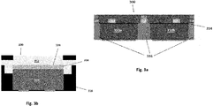
- Figure 3a illustrates a multi-die CSP semiconductor device 300 embodiment, whereby multiple semiconductor dies 310a, 310b are arranged in the CSP semiconductor device 300.
- the dies will be fixed to a carrier 312 using, for example, an epoxy based adhesive.
- the mould material 316 is arranged to separate the multiple dies 310a, 310b. This arrangement may be advantageous, where the semiconductor dies 310a, 310b are arranged in, for example a cascode, or half-bridge configurations.
- Figure 3b illustrate an embodiments, whereby the carrier 312 includes as a recessed portion for accommodating the adhesive 314 and/or an upper portion of the semiconductor die 310.
- the recessed portion of the carrier 312 is sized to receive the semiconductor die 310 and the adhesive 314 arranged thereon.
- the recessed portion 324 of the carrier 312 may be sized to receive the adhesive 314 arranged on the semiconductor die 310.
- the arrangement of Figure 3b may be advantageous in reducing the overall package height of the device 300.
- adhesive bleeds may be prevented by containing the adhesive 314 within the recess 324 of the carrier 312.
- the embodiment of Figure 3b is also amenable to multi-die arrangements such as the arrangement of Figure 3a .
- a metallic frame 411 is arranged on a carrier tape 413.
- the carrier tape 413 prevents mould material from covering the carrier during the moulding process and ensures that, as discussed above with reference to Figures 2a and 2d that the carrier 412 is exposed and protrudes through the top surface 402 of the device 400.
- the metallic frame comprises a repeating matrix of carriers 412 whereby neighbouring carriers are interconnected by connecting members 418 or tie bars.
- the matrix of carriers interconnected by the connecting members 418 may be a linear matrix.
- the matrix of carriers may be n x m matrix, where n is the number of rows in the matrix and m is the number of columns in the matrix, and where n and m are both positive integers, with adjacent carriers 412 connected by connecting members 418.
- the example of Figure 4b illustrates one connecting member 418 connecting adjacent carriers in any row or column.
- the number of connecting members 418 may be greater than one on any one side of the device.
- semiconductor dies 410 are then attached to respective carriers 412 using a die attach material 414, such as an epoxy based adhesive as mentioned above, or any appropriate solder or glue.
- the die attach material may be conductive to enable electrical connection from the carrier 412 to the semiconductor die 410.
- the semiconductor dies 410 are attached top down to the carrier 412. In other words the top major surface of the semiconductor die 410, that is, the major surface opposing the surface having the contacts 406, 408 is affixed to a respective carrier using the adhesive 414.
- the adhesive may then be set or solidified by heat curing.
- Figure 4d illustrates a packaging process known as film assisted moulding (FAM), whereby a protective film 417 is applied over the matrix of attached or fixed dies.
- FAM film assisted moulding
- the matrix is then loaded into a moulding machine whereby the liquefied moulding material is forced into closed mould cavities formed by the protective film 417 and the carrier tape 413.
- the moulding material is then solidified by curing.
- the protective film 417 is also removed.
- the matrix may also undergo a process known as post mould curing to further cure and solidify the liquefied moulding material.
- the carrier tape is removed, by a process known as de-taping, from the moulded matrix as illustrated in Figure 4e .
- de-taping any excess mould material present on the contacts or on the exposed side of the carrier is removed, as illustrated in Figure 4f by a process known as deflashing.
- deflashing the exposed side of the carrier may be marked with device details such as for example a product type, using for example a laser, as illustrated in Figure 4g .
- the moulding may be achieved using an over-moulding process as illustrated in Figure 5a and 5b .
- the mould material 516 is arranged to completely cover the semiconductor dies 510, including the contacts arranged thereon. Following curing of the mould material 516, the mould material is removed until the contacts are exposed using a grinding process.
- individual CSP semiconductor devices 400 are separated by singulation from the matrix arrangement. Singulation is carried out along the sidewall walls of the semiconductor devices 400.
- the singulation process may be any appropriate cutting process, such as laser cutting, plasma cutting, saw cutting or any combination thereof, in order to separate the devices 400.
- the step of singulation severs the connecting members 418 and the mould material 416 of adjacent devices 400. This results in the tabs 218 as discussed above with respect to Figure 2a extending through mould material 416 at the side walls of the device 400.
- the devices may be electrically tested to ensure that they have not been damaged during the packaging process. Following testing the devices may be placed on a carrier tape and loaded on reel in preparation for shipping.
- the CSP semiconductor device provides for improved heat dissipation and structural integrity, without increasing the height of the overall package.
- the CSP device according to embodiments is therefore suited to high power transistor devices.
Landscapes
- Structures Or Materials For Encapsulating Or Coating Semiconductor Devices Or Solid State Devices (AREA)
- Engineering & Computer Science (AREA)
- Microelectronics & Electronic Packaging (AREA)
- Encapsulation Of And Coatings For Semiconductor Or Solid State Devices (AREA)
Abstract
Description
- The present disclosure relates to a semiconductor device and method of manufacture. In particular the present disclosure relates to a chip scale package semiconductor device and associated method of manufacture.
- Chip scale package (CSPs) semiconductor devices are becoming increasingly important for applications which require a small footprint. CSPs are commonly used, for instance, in mobile communications devices such as mobile telephones and portable electronic devices. When a CSP incorporates a power semiconductor device, such as a transistor or diode, they require high performance thermal capacity and heat dissipation because they are required to drain large currents to ground or other rails, to protect devices connected thereto from being damaged. On the other hand, the power devices face challenges to increase structural compactness, which requires on the one hand, to have a very small footprint and package height, and, on the other hand to be protected by a package material. The package material is necessary to protect the device from environmental factors such as moisture. In addition the package material prevents solder pastes used to mount the device to a printed circuit board from contacting and potentially short circuiting the body of the semiconductor die. Such arrangements typically have mould material on six sides of the device and are known as six-sided protected CSP devices.
-
Figure 1 is a cross-sectional view of a conventional six sided protectedCSP device 100. Thesemiconductor device 100 has a topmajor surface 102 and an opposing bottommajor surface 104. On the bottommajor surface 104, theCSP semiconductor device 100 includesmultiple contacts contacts contacts - The
semiconductor device 100 is packaged in amould material 116 using any appropriate mould compound such as an epoxy based material. Themould material 116 is arranged to cover all six sides of thesemiconductor die 110, with the exception of thecontacts - Compared to conventional CSP semiconductor devices without mould compound, conventional six sided protected CSP device suffer from the problem of how to dissipate heat generated in the semiconductor die during operation. This is of particular concern when the semiconductor die is a power device.
- According to an embodiment there is provided a chip scale package semiconductor device, comprising; a semiconductor die having a first major surface and an opposing second major surface, the semiconductor die comprising at least two terminals arranged on the second major surface; a carrier comprising a first major surface and an opposing second major surface, wherein the first major surface of the semiconductor die is mounted on the opposing second major surface of the carrier; and a moulding material partially encapsulating the semiconductor die and the carrier, wherein the first major surface of the carrier extends and is exposed through moulding material, and the at least two terminals are exposed through moulding material on a second side of the device.
- The carrier may extend and be exposed through the moulding material on opposing side walls of the device.
- The first major surface of the carrier may be co-planar with the moulding material on a top major surface of the device.
- The opposing second major surface of the carrier may be arranged as a recess in the carrier. The recess may be arranged to mountably receive the semiconductor die. The recess may be arranged to receive an adhesive layer for mounting the semiconductor die to the carrier.
- A top major surface of the package may comprise the carrier and a second opposing major surface of the package may comprise the terminals and the moulding material. According to an embodiment there is provided a method of manufacturing a chip scale package semiconductor device, the method comprising: providing a semiconductor die having a first major surface and an opposing second major surface, the semiconductor die comprising at least two terminals arranged on the second major surface; providing a carrier comprising a first major surface and an opposing second major surface; mounting the first major surface of the semiconductor die to the opposing second major surface of the carrier; partially encapsulating the semiconductor die and the carrier in a moulding material, wherein the first major surface of the carrier extends and is exposed through moulding material, and the at least two terminals are exposed through moulding material on a second side of the device.
- The semiconductor die and the carrier may be encapsulated such that the first major surface of the carrier is co-planar with the moulding material on a top major surface of the device.
- The first major surface of the semiconductor die may be mounted in recess arranged on the opposing second major surface of the carrier.
- The CSP semiconductor device according to the embodiments provides for improved heat dissipation and structural integrity, without increasing the height of the overall package. The CSP device according to embodiments is therefore suited to high power transistor devices.
- So that the manner in which the features of the present disclosure can be understood in detail, a more particular description is made with reference to embodiments, some of which are illustrated in the appended figures. It is to be noted, however, that the appended figures illustrate only typical embodiments and are therefore not to be considered limiting of its scope. The figures are for facilitating an understanding of the disclosure and thus are not necessarily drawn to scale. Advantages of the subject matter claimed will become apparent to those skilled in the art upon reading this description in conjunction with the accompanying figures, in which like reference numerals have been used to designate like elements, and in which:
-
Figure 1 is a cross-sectional view of a known chip scale package semiconductor device; -
Figure 2a is a cross-sectional of a chip scale package semiconductor device view according to an embodiment; -
Figure 2b is a side view of a chip scale package semiconductor device view according to an embodiment; -
Figure 2c is a bottom view of a chip scale package semiconductor device view according to an embodiment; -
Figure 2d is a top view of a chip scale package semiconductor device view according to an embodiment; -
Figure 3a is a side view of a semiconductor device, incorporating multiple semiconductor dies according to an embodiment; -
Figure 3b is a side view of chip scale package semiconductor device according to an embodiment; -
Figure 4a illustrates the step of arranging a frame arranged on a carrier tape according to an embodiment; -
Figure 4b Illustrates a frame arranged as a repeating matrix of carriers according to an embodiment; -
Figure 4c illustrates the step of arranging semiconductor dies on the carriers according to an embodiment; -
Figure 4d illustrates the step packaging of the semiconductor dies attached to the carriers according to an embodiment; -
Figure 4e illustrates the step of de-taping following packaging according to an embodiment; -
Figure 4f illustrates the step of deflashing following de-taping according to an embodiment; -
Figure 4g illustrates the step of product marking according to an embodiment; -
Figure 4h illustrates an example product marking on the carrier according to an embodiment; -
Figure 5a illustrates an over moulding process for packaging the CSP according to an embodiment; and -
Figure 5b illustrates a grinding process following over moulding according to an embodiment. -
Figure 2a is cross-sectional view of a six-sided Protected Chip Scale Package (CSP)semiconductor device 200 in accordance with an embodiment. TheCSP semiconductor device 200 has a topmajor surface 202 and an opposing bottommajor surface 204. On the bottommajor surface 204, theCSP semiconductor device 200 includes multiple terminals orcontacts terminals semiconductor die 210 of theCSP semiconductor device 200 to external circuit components, such as a printed circuit board (PCB), not illustrated. Thecontacts - The top
major surface 202 of theCSP semiconductor device 200 includes a metal (or plastic)carrier 212 to support thesemiconductor die 210. Thecarrier 212 is fixedly mounted to a top surface of the semiconductor die 210 by any appropriate means, such as an epoxy basedadhesive 214. - Whilst
Figure 2a , illustrates twocontacts semiconductor die 210, the skilled person will recognise that the any number of contacts may be provided dependent on the type and functionality of thesemiconductor die 210. For example, where the semiconductor die is a field effect transistor, the number of contacts may be three, with respective contacts connected to corresponding source, gate and drain terminals of thesemiconductor die 210. The semiconductor die 210 may alternatively be a bipolar junction transistor, thyristor or a two terminal diode. In addition apassivation layer 217 may be included on the surface of the semiconductor die 210 having thecontacts - The
CSP semiconductor device 200 is packaged in amould material 216 using any appropriate mould compound such as an epoxy based material. The mould material may substantially cover the four minor sides of theCSP semiconductor device 200. With the exception of thecontacts mould material 216 may also be formed to cover the bottom major surface of thedevice 200. Themould material 216 may be arranged on the topmajor surface 202 of thedevice 200 so that a top surface of thecarrier 212 is exposed. - The
carrier 212 may also include one ormore metal tabs 218 that extend from each side of thecarrier 212 to protrude through themould material 216 so as to be exposed at opposing sides of theCSP semiconductor device 200. Thetabs 218 are an artefact of the singulation process of theCSP semiconductor device 200, which will be discussed in more detail below. - A side view of
CSP semiconductor device 200 is illustrated inFigure 2b , which shows thetabs 218, protruding through themould material 216 on the side of thedevice 200.Figure 2b illustrates one side of thedevice 200 and the skilled person will appreciate that the corresponding opposing side will have the same arrangement oftabs 218, 220 protruding through themould material 216, due to the matrix arrangement of the carrier as discussed below. -
Figure 2c illustrates a bottom view of theCSP semiconductor device 200 and shows thecontacts mould material 216 arranged on thebottom surface 204 of thedevice 200.Figure 2d illustrates a top view of theCSP semiconductor device 200 and shows thecarrier 212 protrude through themould material 216 such that the carrier is exposed on thetop surface 202 of thedevice 200. Anoptional chamfer 222 may be arranged on thecarrier 212, which may be used to indicate contact polarity and assist in device orientation when placing on PCB. - The arrangement of the
carrier 212 to protrude through thetop surface 202 of thedevice 200 and also through the opposing side walls provides improved thermal characteristics of thedevice 200. The carrier, which acts as a heat sink is exposed, rather than covered by the mould material, and thus any heat generated in the die during operation of the device may be efficiently dissipated away from the semiconductor die 210. This may be particularly advantageous where the device is a high power device. - Furthermore, and as discussed in more detail below with respect to the method of fabrication, the arrangement of the
carrier 212 in thedevice 200, when compared to conventional devices, is provided without increasing the overall package height of thedevice 200. - Furthermore, the
carrier 212 also provides mechanical strength to thedevice 200 by supporting the semiconductor die 210. This is particularly advantageous where thedevice 200 is used in harsh environmental conditions such as in automotive applications. -
Figure 3a illustrates a multi-dieCSP semiconductor device 300 embodiment, whereby multiple semiconductor dies 310a, 310b are arranged in theCSP semiconductor device 300. As with the previous embodiment, the dies will be fixed to acarrier 312 using, for example, an epoxy based adhesive. Themould material 316 is arranged to separate the multiple dies 310a, 310b. This arrangement may be advantageous, where the semiconductor dies 310a, 310b are arranged in, for example a cascode, or half-bridge configurations. -
Figure 3b illustrate an embodiments, whereby thecarrier 312 includes as a recessed portion for accommodating the adhesive 314 and/or an upper portion of the semiconductor die 310. In the embodiment ofFigure 3b the recessed portion of thecarrier 312 is sized to receive the semiconductor die 310 and the adhesive 314 arranged thereon. Alternatively, the recessedportion 324 of thecarrier 312 may be sized to receive the adhesive 314 arranged on the semiconductor die 310. The arrangement ofFigure 3b may be advantageous in reducing the overall package height of thedevice 300. In addition adhesive bleeds may be prevented by containing the adhesive 314 within therecess 324 of thecarrier 312. The skilled person will also understand that the embodiment ofFigure 3b is also amenable to multi-die arrangements such as the arrangement ofFigure 3a . - An example process flow for manufacturing the semiconductor device according to the above embodiments will now be described with reference to
Figures 4a to 4h which illustrates example process steps. - With reference to
Figure 4a , ametallic frame 411 is arranged on acarrier tape 413. Thecarrier tape 413 prevents mould material from covering the carrier during the moulding process and ensures that, as discussed above with reference toFigures 2a and2d that thecarrier 412 is exposed and protrudes through thetop surface 402 of thedevice 400. The metallic frame comprises a repeating matrix ofcarriers 412 whereby neighbouring carriers are interconnected by connectingmembers 418 or tie bars. The matrix of carriers interconnected by the connectingmembers 418 may be a linear matrix. Alternatively, and as illustrated in the plan view ofFigure 4b , the matrix of carriers may be n x m matrix, where n is the number of rows in the matrix and m is the number of columns in the matrix, and where n and m are both positive integers, withadjacent carriers 412 connected by connectingmembers 418. The example ofFigure 4b illustrates one connectingmember 418 connecting adjacent carriers in any row or column. However, consistent with the example ofFigure 2b , the skilled person will appreciate the number of connectingmembers 418 may be greater than one on any one side of the device. - As illustrated in
Figure 4c , semiconductor dies 410 are then attached torespective carriers 412 using a die attachmaterial 414, such as an epoxy based adhesive as mentioned above, or any appropriate solder or glue. In certain applications the die attach material may be conductive to enable electrical connection from thecarrier 412 to the semiconductor die 410. It should be noted that the semiconductor dies 410 are attached top down to thecarrier 412. In other words the top major surface of the semiconductor die 410, that is, the major surface opposing the surface having thecontacts - Following the semiconductor die 410 attach process discussed above, the arrangement of semiconductor dies attached to the carriers is then packaged.
Figure 4d illustrates a packaging process known as film assisted moulding (FAM), whereby aprotective film 417 is applied over the matrix of attached or fixed dies. The matrix is then loaded into a moulding machine whereby the liquefied moulding material is forced into closed mould cavities formed by theprotective film 417 and thecarrier tape 413. The moulding material is then solidified by curing. - When the moulded matrix is removed from the moulding machine the
protective film 417 is also removed. Following the moulding process, the matrix may also undergo a process known as post mould curing to further cure and solidify the liquefied moulding material. - Following moulding and curing, the carrier tape is removed, by a process known as de-taping, from the moulded matrix as illustrated in
Figure 4e . When de-taping is completed, any excess mould material present on the contacts or on the exposed side of the carrier is removed, as illustrated inFigure 4f by a process known as deflashing. Once deflashing is completed the exposed side of the carrier may be marked with device details such as for example a product type, using for example a laser, as illustrated inFigure 4g . - As an alternative to the FAM process mentioned above, the moulding may be achieved using an over-moulding process as illustrated in
Figure 5a and 5b . In the over-moulding process, themould material 516 is arranged to completely cover the semiconductor dies 510, including the contacts arranged thereon. Following curing of themould material 516, the mould material is removed until the contacts are exposed using a grinding process. - Following marking, individual
CSP semiconductor devices 400 are separated by singulation from the matrix arrangement. Singulation is carried out along the sidewall walls of thesemiconductor devices 400. The singulation process may be any appropriate cutting process, such as laser cutting, plasma cutting, saw cutting or any combination thereof, in order to separate thedevices 400. The step of singulation severs the connectingmembers 418 and themould material 416 ofadjacent devices 400. This results in thetabs 218 as discussed above with respect toFigure 2a extending throughmould material 416 at the side walls of thedevice 400. - Following singulation, the devices may be electrically tested to ensure that they have not been damaged during the packaging process. Following testing the devices may be placed on a carrier tape and loaded on reel in preparation for shipping.
- The CSP semiconductor device according to the embodiments provides for improved heat dissipation and structural integrity, without increasing the height of the overall package. The CSP device according to embodiments is therefore suited to high power transistor devices.
- Particular and preferred aspects of the invention are set out in the accompanying independent claims. Combinations of features from the dependent and/or independent claims may be combined as appropriate and not merely as set out in the claims.
- The scope of the present disclosure includes any novel feature or combination of features disclosed therein either explicitly or implicitly or any generalisation thereof irrespective of whether or not it relates to the claimed invention or mitigate against any or all of the problems addressed by the present invention. The applicant hereby gives notice that new claims may be formulated to such features during prosecution of this application or of any such further application derived there from. In particular, with reference to the appended claims, features from dependent claims may be combined with those of the independent claims and features from respective independent claims may be combined in any appropriate manner and not merely in specific combinations enumerated in the claims.
- Features which are described in the context of separate embodiments may also be provided in combination in a single embodiment. Conversely, various features which are, for brevity, described in the context of a single embodiment, may also be provided separately or in any suitable sub combination.
- Term "comprising" does not exclude other elements or steps, the term "a" or "an" does not exclude a plurality. Reference signs in the claims shall not be construed as limiting the scope of the claims.
Claims (10)
- A chip scale package semiconductor device, comprising;
a semiconductor die having a first major surface and an opposing second major surface, the semiconductor die comprising at least two terminals arranged on the second major surface;
a carrier comprising a first major surface and an opposing second major surface, wherein the first major surface of the semiconductor die is mounted on the opposing second major surface of the carrier; and
a moulding material partially encapsulating the semiconductor die and the carrier, wherein the first major surface of the carrier extends and is exposed through moulding material, and the at least two terminals are exposed through moulding material on a second side of the device. - The chip scale package semiconductor device of claim 1, wherein the carrier extends and is exposed through the moulding material on opposing side walls of the device.
- The chip scale package semiconductor device of claim 1, wherein the first major surface of the carrier is co-planar with the moulding material on a top major surface of the device.
- The chip scale package semiconductor device of any preceding claim, wherein the opposing second major surface of the carrier is arranged as a recess in the carrier.
- The chip scale package of claim 4, wherein the recess is arranged to mountably receive the semiconductor die.
- The chip scale package of claim 4, wherein the recess is arranged to receive an adhesive layer for mounting the semiconductor die to the carrier.
- The chip scale semiconductor package of any preceding claim, wherein a top major surface of the package comprises the carrier and a second opposing major surface of the package comprises the terminals and the moulding material.
- A method of manufacturing a chip scale package semiconductor device, the method comprising:providing a semiconductor die having a first major surface and an opposing second major surface, the semiconductor die comprising at least two terminals arranged on the second major surface;providing a carrier comprising a first major surface and an opposing second major surface;mounting the first major surface of the semiconductor die to the opposing second major surface of the carrier;partially encapsulating the semiconductor die and the carrier in a moulding material, wherein the first major surface of the carrier extends and is exposed through moulding material, and the at least two terminals are exposed through moulding material on a second side of the device.
- The method of claim 8, wherein the semiconductor die and the carrier are encapsulated such that the first major surface of the carrier is co-planar with the moulding material on a top major surface of the device.
- The method of claim 8 or 9, wherein the first major surface of the semiconductor die is mounted a recess arranged on the opposing second major surface of the carrier.
Applications Claiming Priority (1)
| Application Number | Priority Date | Filing Date | Title |
|---|---|---|---|
| CN201711383469.8A CN109950214A (en) | 2017-12-20 | 2017-12-20 | Chip-scale packaged semiconductor device and method of making the same |
Publications (2)
| Publication Number | Publication Date |
|---|---|
| EP3503177A1 true EP3503177A1 (en) | 2019-06-26 |
| EP3503177B1 EP3503177B1 (en) | 2025-07-09 |
Family
ID=64082888
Family Applications (1)
| Application Number | Title | Priority Date | Filing Date |
|---|---|---|---|
| EP18202874.6A Active EP3503177B1 (en) | 2017-12-20 | 2018-10-26 | Carrier protected chip scale package and method of manufacturing thereof |
Country Status (3)
| Country | Link |
|---|---|
| US (1) | US11817360B2 (en) |
| EP (1) | EP3503177B1 (en) |
| CN (2) | CN109950214A (en) |
Families Citing this family (1)
| Publication number | Priority date | Publication date | Assignee | Title |
|---|---|---|---|---|
| US11018030B2 (en) * | 2019-03-20 | 2021-05-25 | Semiconductor Components Industries, Llc | Fan-out wafer level chip-scale packages and methods of manufacture |
Citations (3)
| Publication number | Priority date | Publication date | Assignee | Title |
|---|---|---|---|---|
| US6707148B1 (en) * | 2002-05-21 | 2004-03-16 | National Semiconductor Corporation | Bumped integrated circuits for optical applications |
| US20120217629A1 (en) * | 2011-02-25 | 2012-08-30 | Stats Chippac, Ltd. | Semiconductor Device and Method of Forming a Wafer Level Package Structure Using Conductive Via and Exposed Bump |
| US20130147054A1 (en) * | 2011-12-08 | 2013-06-13 | Stats Chippac, Ltd. | Semiconductor Device and Method of Forming Thick Encapsulant for Stiffness with Recesses for Stress Relief in FO-WLCSP |
Family Cites Families (23)
| Publication number | Priority date | Publication date | Assignee | Title |
|---|---|---|---|---|
| KR970010678B1 (en) * | 1994-03-30 | 1997-06-30 | 엘지반도체 주식회사 | Lead frame and the package thereof |
| JPH09260568A (en) * | 1996-03-27 | 1997-10-03 | Mitsubishi Electric Corp | Semiconductor device and manufacturing method thereof |
| JP3842444B2 (en) * | 1998-07-24 | 2006-11-08 | 富士通株式会社 | Manufacturing method of semiconductor device |
| US6495944B2 (en) * | 2001-04-18 | 2002-12-17 | International Business Machines Corporation | Electrostatic microactuator with viscous liquid damping |
| US6709897B2 (en) * | 2002-01-15 | 2004-03-23 | Unimicron Technology Corp. | Method of forming IC package having upward-facing chip cavity |
| JP3844467B2 (en) * | 2003-01-08 | 2006-11-15 | 沖電気工業株式会社 | Semiconductor device and manufacturing method thereof |
| TWI367566B (en) * | 2004-05-06 | 2012-07-01 | United Test And Assembly Ct | Structurally-enhanced integrated circuit package and method of manufacture |
| JP2006339354A (en) * | 2005-06-01 | 2006-12-14 | Tdk Corp | SEMICONDUCTOR IC AND ITS MANUFACTURING METHOD, SEMICONDUCTOR IC BUILT-IN MODULE, AND ITS MANUFACTURING METHOD |
| US7385299B2 (en) * | 2006-02-25 | 2008-06-10 | Stats Chippac Ltd. | Stackable integrated circuit package system with multiple interconnect interface |
| US7476980B2 (en) * | 2006-06-27 | 2009-01-13 | Infineon Technologies Ag | Die configurations and methods of manufacture |
| US7968378B2 (en) * | 2008-02-06 | 2011-06-28 | Infineon Technologies Ag | Electronic device |
| KR101009130B1 (en) * | 2009-02-05 | 2011-01-18 | 삼성전기주식회사 | Wafer level heat dissipation package and its manufacturing method |
| US10373870B2 (en) * | 2010-02-16 | 2019-08-06 | Deca Technologies Inc. | Semiconductor device and method of packaging |
| US8822281B2 (en) * | 2010-02-23 | 2014-09-02 | Stats Chippac, Ltd. | Semiconductor device and method of forming TMV and TSV in WLCSP using same carrier |
| US8853003B2 (en) * | 2011-08-09 | 2014-10-07 | Alpha & Omega Semiconductor, Inc. | Wafer level chip scale package with thick bottom metal exposed and preparation method thereof |
| US20130187284A1 (en) * | 2012-01-24 | 2013-07-25 | Broadcom Corporation | Low Cost and High Performance Flip Chip Package |
| US9721862B2 (en) * | 2013-01-03 | 2017-08-01 | STATS ChipPAC Pte. Ltd. | Semiconductor device and method of using a standardized carrier to form embedded wafer level chip scale packages |
| US9087828B2 (en) * | 2013-03-12 | 2015-07-21 | Alpha & Omega Semiconductor Incorporated | Semiconductor device with thick bottom metal and preparation method thereof |
| US9355997B2 (en) * | 2014-03-12 | 2016-05-31 | Invensas Corporation | Integrated circuit assemblies with reinforcement frames, and methods of manufacture |
| JP6421050B2 (en) * | 2015-02-09 | 2018-11-07 | 株式会社ジェイデバイス | Semiconductor device |
| KR101731700B1 (en) * | 2015-03-18 | 2017-04-28 | 앰코 테크놀로지 코리아 주식회사 | Semiconductor device and manufacturing method thereof |
| KR20160143264A (en) * | 2015-06-05 | 2016-12-14 | 주식회사 에스에프에이반도체 | Fan-out wafer level package and method for manufacturing the same |
| JP6605382B2 (en) * | 2016-03-30 | 2019-11-13 | 新光電気工業株式会社 | Semiconductor device and manufacturing method of semiconductor device |
-
2017
- 2017-12-20 CN CN201711383469.8A patent/CN109950214A/en active Pending
- 2017-12-20 CN CN202410396027.0A patent/CN118263196B/en active Active
-
2018
- 2018-10-26 EP EP18202874.6A patent/EP3503177B1/en active Active
- 2018-12-14 US US16/220,160 patent/US11817360B2/en active Active
Patent Citations (3)
| Publication number | Priority date | Publication date | Assignee | Title |
|---|---|---|---|---|
| US6707148B1 (en) * | 2002-05-21 | 2004-03-16 | National Semiconductor Corporation | Bumped integrated circuits for optical applications |
| US20120217629A1 (en) * | 2011-02-25 | 2012-08-30 | Stats Chippac, Ltd. | Semiconductor Device and Method of Forming a Wafer Level Package Structure Using Conductive Via and Exposed Bump |
| US20130147054A1 (en) * | 2011-12-08 | 2013-06-13 | Stats Chippac, Ltd. | Semiconductor Device and Method of Forming Thick Encapsulant for Stiffness with Recesses for Stress Relief in FO-WLCSP |
Also Published As
| Publication number | Publication date |
|---|---|
| CN118263196B (en) | 2026-01-30 |
| US11817360B2 (en) | 2023-11-14 |
| EP3503177B1 (en) | 2025-07-09 |
| US20190189530A1 (en) | 2019-06-20 |
| CN109950214A (en) | 2019-06-28 |
| CN118263196A (en) | 2024-06-28 |
Similar Documents
| Publication | Publication Date | Title |
|---|---|---|
| US7968982B2 (en) | Thermal enhanced upper and dual heat sink exposed molded leadless package | |
| US11842948B2 (en) | SMDs integration on QFN by 3D stacked solution | |
| US7495323B2 (en) | Semiconductor package structure having multiple heat dissipation paths and method of manufacture | |
| US7902649B2 (en) | Leadframe for leadless package, structure and manufacturing method using the same | |
| US20210118778A1 (en) | Semiconductor package having a lead frame and a heat-sink lead frame | |
| CN102420217A (en) | Multi-chip semiconductor packages and assembly thereof | |
| US10256168B2 (en) | Semiconductor device and lead frame therefor | |
| KR20070034438A (en) | Method of making a stacked die package | |
| US11984388B2 (en) | Semiconductor package structures and methods of manufacture | |
| US11817360B2 (en) | Chip scale package semiconductor device and method of manufacture | |
| US7517729B2 (en) | Integrated circuit package system with heat slug | |
| CN212625552U (en) | Semiconductor chip packaging structure and electronic equipment | |
| US4910581A (en) | Internally molded isolated package | |
| CN108352364B (en) | air cavity package | |
| KR20180062479A (en) | Semiconductor package and a method of manufacturing the same | |
| US10522448B2 (en) | Single or multi chip module package and related methods | |
| KR100206880B1 (en) | Columnar package with heat sink | |
| US7084003B2 (en) | Method for manufacturing semiconductor device packages | |
| KR19980083733A (en) | Thin Film Ball Grid Array Package with Improved Thermal Dissipation | |
| US20260090449A1 (en) | Semiconductor Package | |
| US20240429135A1 (en) | Method for manufacturing a semiconductor package assembly as well as a semiconductor package assembly obtained with this method | |
| KR102340866B1 (en) | Semiconductor package and a method of manufacturing the same | |
| GB2603920A (en) | Power Semiconductor Package | |
| CN104637911A (en) | Lead frame-based semiconductor device with routing substrate |
Legal Events
| Date | Code | Title | Description |
|---|---|---|---|
| PUAI | Public reference made under article 153(3) epc to a published international application that has entered the european phase |
Free format text: ORIGINAL CODE: 0009012 |
|
| STAA | Information on the status of an ep patent application or granted ep patent |
Free format text: STATUS: THE APPLICATION HAS BEEN PUBLISHED |
|
| AK | Designated contracting states |
Kind code of ref document: A1 Designated state(s): AL AT BE BG CH CY CZ DE DK EE ES FI FR GB GR HR HU IE IS IT LI LT LU LV MC MK MT NL NO PL PT RO RS SE SI SK SM TR |
|
| AX | Request for extension of the european patent |
Extension state: BA ME |
|
| STAA | Information on the status of an ep patent application or granted ep patent |
Free format text: STATUS: REQUEST FOR EXAMINATION WAS MADE |
|
| 17P | Request for examination filed |
Effective date: 20191211 |
|
| RBV | Designated contracting states (corrected) |
Designated state(s): AL AT BE BG CH CY CZ DE DK EE ES FI FR GB GR HR HU IE IS IT LI LT LU LV MC MK MT NL NO PL PT RO RS SE SI SK SM TR |
|
| STAA | Information on the status of an ep patent application or granted ep patent |
Free format text: STATUS: EXAMINATION IS IN PROGRESS |
|
| 17Q | First examination report despatched |
Effective date: 20210720 |
|
| GRAP | Despatch of communication of intention to grant a patent |
Free format text: ORIGINAL CODE: EPIDOSNIGR1 |
|
| STAA | Information on the status of an ep patent application or granted ep patent |
Free format text: STATUS: GRANT OF PATENT IS INTENDED |
|
| RIC1 | Information provided on ipc code assigned before grant |
Ipc: H01L 23/544 20060101ALI20250123BHEP Ipc: H01L 23/16 20060101ALI20250123BHEP Ipc: H01L 21/56 20060101ALI20250123BHEP Ipc: H01L 23/31 20060101AFI20250123BHEP |
|
| INTG | Intention to grant announced |
Effective date: 20250213 |
|
| GRAS | Grant fee paid |
Free format text: ORIGINAL CODE: EPIDOSNIGR3 |
|
| GRAA | (expected) grant |
Free format text: ORIGINAL CODE: 0009210 |
|
| STAA | Information on the status of an ep patent application or granted ep patent |
Free format text: STATUS: THE PATENT HAS BEEN GRANTED |
|
| AK | Designated contracting states |
Kind code of ref document: B1 Designated state(s): AL AT BE BG CH CY CZ DE DK EE ES FI FR GB GR HR HU IE IS IT LI LT LU LV MC MK MT NL NO PL PT RO RS SE SI SK SM TR |
|
| REG | Reference to a national code |
Ref country code: GB Ref legal event code: FG4D |
|
| REG | Reference to a national code |
Ref country code: CH Ref legal event code: EP |
|
| REG | Reference to a national code |
Ref country code: IE Ref legal event code: FG4D |
|
| REG | Reference to a national code |
Ref country code: DE Ref legal event code: R096 Ref document number: 602018083375 Country of ref document: DE |
|
| REG | Reference to a national code |
Ref country code: NL Ref legal event code: MP Effective date: 20250709 |
|
| REG | Reference to a national code |
Ref country code: DE Ref legal event code: R079 Ref document number: 602018083375 Country of ref document: DE Free format text: PREVIOUS MAIN CLASS: H01L0023310000 Ipc: H10W0074100000 |
|
| PG25 | Lapsed in a contracting state [announced via postgrant information from national office to epo] |
Ref country code: PT Free format text: LAPSE BECAUSE OF FAILURE TO SUBMIT A TRANSLATION OF THE DESCRIPTION OR TO PAY THE FEE WITHIN THE PRESCRIBED TIME-LIMIT Effective date: 20251110 |
|
| PG25 | Lapsed in a contracting state [announced via postgrant information from national office to epo] |
Ref country code: NL Free format text: LAPSE BECAUSE OF FAILURE TO SUBMIT A TRANSLATION OF THE DESCRIPTION OR TO PAY THE FEE WITHIN THE PRESCRIBED TIME-LIMIT Effective date: 20250709 |
|
| REG | Reference to a national code |
Ref country code: AT Ref legal event code: MK05 Ref document number: 1812724 Country of ref document: AT Kind code of ref document: T Effective date: 20250709 |
|
| PG25 | Lapsed in a contracting state [announced via postgrant information from national office to epo] |
Ref country code: IS Free format text: LAPSE BECAUSE OF FAILURE TO SUBMIT A TRANSLATION OF THE DESCRIPTION OR TO PAY THE FEE WITHIN THE PRESCRIBED TIME-LIMIT Effective date: 20251109 |
|
| PGFP | Annual fee paid to national office [announced via postgrant information from national office to epo] |
Ref country code: DE Payment date: 20251028 Year of fee payment: 8 |
|
| PG25 | Lapsed in a contracting state [announced via postgrant information from national office to epo] |
Ref country code: NO Free format text: LAPSE BECAUSE OF FAILURE TO SUBMIT A TRANSLATION OF THE DESCRIPTION OR TO PAY THE FEE WITHIN THE PRESCRIBED TIME-LIMIT Effective date: 20251009 |
|
| REG | Reference to a national code |
Ref country code: LT Ref legal event code: MG9D |
|
| PG25 | Lapsed in a contracting state [announced via postgrant information from national office to epo] |
Ref country code: AT Free format text: LAPSE BECAUSE OF FAILURE TO SUBMIT A TRANSLATION OF THE DESCRIPTION OR TO PAY THE FEE WITHIN THE PRESCRIBED TIME-LIMIT Effective date: 20250709 |
|
| PG25 | Lapsed in a contracting state [announced via postgrant information from national office to epo] |
Ref country code: FI Free format text: LAPSE BECAUSE OF FAILURE TO SUBMIT A TRANSLATION OF THE DESCRIPTION OR TO PAY THE FEE WITHIN THE PRESCRIBED TIME-LIMIT Effective date: 20250709 |
|
| PG25 | Lapsed in a contracting state [announced via postgrant information from national office to epo] |
Ref country code: HR Free format text: LAPSE BECAUSE OF FAILURE TO SUBMIT A TRANSLATION OF THE DESCRIPTION OR TO PAY THE FEE WITHIN THE PRESCRIBED TIME-LIMIT Effective date: 20250709 |
|
| PG25 | Lapsed in a contracting state [announced via postgrant information from national office to epo] |
Ref country code: GR Free format text: LAPSE BECAUSE OF FAILURE TO SUBMIT A TRANSLATION OF THE DESCRIPTION OR TO PAY THE FEE WITHIN THE PRESCRIBED TIME-LIMIT Effective date: 20251010 |
|
| PG25 | Lapsed in a contracting state [announced via postgrant information from national office to epo] |
Ref country code: SE Free format text: LAPSE BECAUSE OF FAILURE TO SUBMIT A TRANSLATION OF THE DESCRIPTION OR TO PAY THE FEE WITHIN THE PRESCRIBED TIME-LIMIT Effective date: 20250709 |
|
| PG25 | Lapsed in a contracting state [announced via postgrant information from national office to epo] |
Ref country code: LV Free format text: LAPSE BECAUSE OF FAILURE TO SUBMIT A TRANSLATION OF THE DESCRIPTION OR TO PAY THE FEE WITHIN THE PRESCRIBED TIME-LIMIT Effective date: 20250709 |
|
| PG25 | Lapsed in a contracting state [announced via postgrant information from national office to epo] |
Ref country code: BG Free format text: LAPSE BECAUSE OF FAILURE TO SUBMIT A TRANSLATION OF THE DESCRIPTION OR TO PAY THE FEE WITHIN THE PRESCRIBED TIME-LIMIT Effective date: 20250709 Ref country code: PL Free format text: LAPSE BECAUSE OF FAILURE TO SUBMIT A TRANSLATION OF THE DESCRIPTION OR TO PAY THE FEE WITHIN THE PRESCRIBED TIME-LIMIT Effective date: 20250709 |
|
| PG25 | Lapsed in a contracting state [announced via postgrant information from national office to epo] |
Ref country code: RS Free format text: LAPSE BECAUSE OF FAILURE TO SUBMIT A TRANSLATION OF THE DESCRIPTION OR TO PAY THE FEE WITHIN THE PRESCRIBED TIME-LIMIT Effective date: 20251009 |
|
| PG25 | Lapsed in a contracting state [announced via postgrant information from national office to epo] |
Ref country code: ES Free format text: LAPSE BECAUSE OF FAILURE TO SUBMIT A TRANSLATION OF THE DESCRIPTION OR TO PAY THE FEE WITHIN THE PRESCRIBED TIME-LIMIT Effective date: 20250709 |
|
| PG25 | Lapsed in a contracting state [announced via postgrant information from national office to epo] |
Ref country code: RO Free format text: LAPSE BECAUSE OF FAILURE TO SUBMIT A TRANSLATION OF THE DESCRIPTION OR TO PAY THE FEE WITHIN THE PRESCRIBED TIME-LIMIT Effective date: 20250709 |
|
| PG25 | Lapsed in a contracting state [announced via postgrant information from national office to epo] |
Ref country code: SM Free format text: LAPSE BECAUSE OF FAILURE TO SUBMIT A TRANSLATION OF THE DESCRIPTION OR TO PAY THE FEE WITHIN THE PRESCRIBED TIME-LIMIT Effective date: 20250709 |
|
| REG | Reference to a national code |
Ref country code: DE Ref legal event code: R097 Ref document number: 602018083375 Country of ref document: DE |
|
| PG25 | Lapsed in a contracting state [announced via postgrant information from national office to epo] |
Ref country code: DK Free format text: LAPSE BECAUSE OF FAILURE TO SUBMIT A TRANSLATION OF THE DESCRIPTION OR TO PAY THE FEE WITHIN THE PRESCRIBED TIME-LIMIT Effective date: 20250709 |
|
| PG25 | Lapsed in a contracting state [announced via postgrant information from national office to epo] |
Ref country code: IT Free format text: LAPSE BECAUSE OF FAILURE TO SUBMIT A TRANSLATION OF THE DESCRIPTION OR TO PAY THE FEE WITHIN THE PRESCRIBED TIME-LIMIT Effective date: 20250709 |
|
| PG25 | Lapsed in a contracting state [announced via postgrant information from national office to epo] |
Ref country code: CZ Free format text: LAPSE BECAUSE OF FAILURE TO SUBMIT A TRANSLATION OF THE DESCRIPTION OR TO PAY THE FEE WITHIN THE PRESCRIBED TIME-LIMIT Effective date: 20250709 |
|
| PG25 | Lapsed in a contracting state [announced via postgrant information from national office to epo] |
Ref country code: EE Free format text: LAPSE BECAUSE OF FAILURE TO SUBMIT A TRANSLATION OF THE DESCRIPTION OR TO PAY THE FEE WITHIN THE PRESCRIBED TIME-LIMIT Effective date: 20250709 Ref country code: SK Free format text: LAPSE BECAUSE OF FAILURE TO SUBMIT A TRANSLATION OF THE DESCRIPTION OR TO PAY THE FEE WITHIN THE PRESCRIBED TIME-LIMIT Effective date: 20250709 |
|
| PLBE | No opposition filed within time limit |
Free format text: ORIGINAL CODE: 0009261 |
|
| STAA | Information on the status of an ep patent application or granted ep patent |
Free format text: STATUS: NO OPPOSITION FILED WITHIN TIME LIMIT |
|
| REG | Reference to a national code |
Ref country code: CH Ref legal event code: L10 Free format text: ST27 STATUS EVENT CODE: U-0-0-L10-L00 (AS PROVIDED BY THE NATIONAL OFFICE) Effective date: 20260521 |
|
| REG | Reference to a national code |
Ref country code: CH Ref legal event code: H13 Free format text: ST27 STATUS EVENT CODE: U-0-0-H10-H13 (AS PROVIDED BY THE NATIONAL OFFICE) Effective date: 20260527 |
|
| PG25 | Lapsed in a contracting state [announced via postgrant information from national office to epo] |
Ref country code: LU Free format text: LAPSE BECAUSE OF NON-PAYMENT OF DUE FEES Effective date: 20251026 |
|
| 26N | No opposition filed |
Effective date: 20260410 |
|
| REG | Reference to a national code |
Ref country code: BE Ref legal event code: MM Effective date: 20251031 |
|
| GBPC | Gb: european patent ceased through non-payment of renewal fee |
Effective date: 20251026 |
|
| PG25 | Lapsed in a contracting state [announced via postgrant information from national office to epo] |
Ref country code: LT Free format text: LAPSE BECAUSE OF FAILURE TO SUBMIT A TRANSLATION OF THE DESCRIPTION OR TO PAY THE FEE WITHIN THE PRESCRIBED TIME-LIMIT Effective date: 20250709 Ref country code: MC Free format text: LAPSE BECAUSE OF FAILURE TO SUBMIT A TRANSLATION OF THE DESCRIPTION OR TO PAY THE FEE WITHIN THE PRESCRIBED TIME-LIMIT Effective date: 20250709 |
|
| PG25 | Lapsed in a contracting state [announced via postgrant information from national office to epo] |
Ref country code: GB Free format text: LAPSE BECAUSE OF NON-PAYMENT OF DUE FEES Effective date: 20251026 |
|
| PG25 | Lapsed in a contracting state [announced via postgrant information from national office to epo] |
Ref country code: CH Free format text: LAPSE BECAUSE OF NON-PAYMENT OF DUE FEES Effective date: 20251031 Ref country code: BE Free format text: LAPSE BECAUSE OF NON-PAYMENT OF DUE FEES Effective date: 20251031 |
|
| PG25 | Lapsed in a contracting state [announced via postgrant information from national office to epo] |
Ref country code: FR Free format text: LAPSE BECAUSE OF NON-PAYMENT OF DUE FEES Effective date: 20251031 |