EP3502854A1 - Non-orthogonal demodulation module, touch-control system and non-orthogonal demodulation method - Google Patents
Non-orthogonal demodulation module, touch-control system and non-orthogonal demodulation method Download PDFInfo
- Publication number
- EP3502854A1 EP3502854A1 EP17909664.9A EP17909664A EP3502854A1 EP 3502854 A1 EP3502854 A1 EP 3502854A1 EP 17909664 A EP17909664 A EP 17909664A EP 3502854 A1 EP3502854 A1 EP 3502854A1
- Authority
- EP
- European Patent Office
- Prior art keywords
- calibration
- frequencies
- quadrature
- frequency
- phase
- Prior art date
- Legal status (The legal status is an assumption and is not a legal conclusion. Google has not performed a legal analysis and makes no representation as to the accuracy of the status listed.)
- Granted
Links
Images



Classifications
-
- G—PHYSICS
- G06—COMPUTING OR CALCULATING; COUNTING
- G06F—ELECTRIC DIGITAL DATA PROCESSING
- G06F3/00—Input arrangements for transferring data to be processed into a form capable of being handled by the computer; Output arrangements for transferring data from processing unit to output unit, e.g. interface arrangements
- G06F3/01—Input arrangements or combined input and output arrangements for interaction between user and computer
- G06F3/03—Arrangements for converting the position or the displacement of a member into a coded form
- G06F3/041—Digitisers, e.g. for touch screens or touch pads, characterised by the transducing means
-
- G—PHYSICS
- G06—COMPUTING OR CALCULATING; COUNTING
- G06F—ELECTRIC DIGITAL DATA PROCESSING
- G06F3/00—Input arrangements for transferring data to be processed into a form capable of being handled by the computer; Output arrangements for transferring data from processing unit to output unit, e.g. interface arrangements
- G06F3/01—Input arrangements or combined input and output arrangements for interaction between user and computer
- G06F3/03—Arrangements for converting the position or the displacement of a member into a coded form
- G06F3/041—Digitisers, e.g. for touch screens or touch pads, characterised by the transducing means
- G06F3/0416—Control or interface arrangements specially adapted for digitisers
- G06F3/04166—Details of scanning methods, e.g. sampling time, grouping of sub areas or time sharing with display driving
-
- G—PHYSICS
- G06—COMPUTING OR CALCULATING; COUNTING
- G06F—ELECTRIC DIGITAL DATA PROCESSING
- G06F3/00—Input arrangements for transferring data to be processed into a form capable of being handled by the computer; Output arrangements for transferring data from processing unit to output unit, e.g. interface arrangements
- G06F3/01—Input arrangements or combined input and output arrangements for interaction between user and computer
- G06F3/03—Arrangements for converting the position or the displacement of a member into a coded form
- G06F3/041—Digitisers, e.g. for touch screens or touch pads, characterised by the transducing means
- G06F3/0416—Control or interface arrangements specially adapted for digitisers
-
- H—ELECTRICITY
- H04—ELECTRIC COMMUNICATION TECHNIQUE
- H04L—TRANSMISSION OF DIGITAL INFORMATION, e.g. TELEGRAPHIC COMMUNICATION
- H04L27/00—Modulated-carrier systems
- H04L27/18—Phase-modulated carrier systems, i.e. using phase-shift keying
- H04L27/22—Demodulator circuits; Receiver circuits
-
- G—PHYSICS
- G06—COMPUTING OR CALCULATING; COUNTING
- G06F—ELECTRIC DIGITAL DATA PROCESSING
- G06F3/00—Input arrangements for transferring data to be processed into a form capable of being handled by the computer; Output arrangements for transferring data from processing unit to output unit, e.g. interface arrangements
- G06F3/01—Input arrangements or combined input and output arrangements for interaction between user and computer
- G06F3/03—Arrangements for converting the position or the displacement of a member into a coded form
- G06F3/041—Digitisers, e.g. for touch screens or touch pads, characterised by the transducing means
- G06F3/044—Digitisers, e.g. for touch screens or touch pads, characterised by the transducing means by capacitive means
- G06F3/0446—Digitisers, e.g. for touch screens or touch pads, characterised by the transducing means by capacitive means using a grid-like structure of electrodes in at least two directions, e.g. using row and column electrodes
-
- H—ELECTRICITY
- H03—ELECTRONIC CIRCUITRY
- H03K—PULSE TECHNIQUE
- H03K9/00—Demodulating pulses which have been modulated with a continuously-variable signal
-
- H—ELECTRICITY
- H04—ELECTRIC COMMUNICATION TECHNIQUE
- H04L—TRANSMISSION OF DIGITAL INFORMATION, e.g. TELEGRAPHIC COMMUNICATION
- H04L27/00—Modulated-carrier systems
- H04L27/10—Frequency-modulated carrier systems, i.e. using frequency-shift keying
- H04L27/14—Demodulator circuits; Receiver circuits
-
- H—ELECTRICITY
- H04—ELECTRIC COMMUNICATION TECHNIQUE
- H04L—TRANSMISSION OF DIGITAL INFORMATION, e.g. TELEGRAPHIC COMMUNICATION
- H04L27/00—Modulated-carrier systems
- H04L27/18—Phase-modulated carrier systems, i.e. using phase-shift keying
- H04L27/22—Demodulator circuits; Receiver circuits
- H04L27/233—Demodulator circuits; Receiver circuits using non-coherent demodulation
-
- H—ELECTRICITY
- H04—ELECTRIC COMMUNICATION TECHNIQUE
- H04L—TRANSMISSION OF DIGITAL INFORMATION, e.g. TELEGRAPHIC COMMUNICATION
- H04L27/00—Modulated-carrier systems
- H04L27/32—Carrier systems characterised by combinations of two or more of the types covered by groups H04L27/02, H04L27/10, H04L27/18 or H04L27/26
- H04L27/34—Amplitude- and phase-modulated carrier systems, e.g. quadrature-amplitude modulated carrier systems
- H04L27/38—Demodulator circuits; Receiver circuits
-
- H—ELECTRICITY
- H04—ELECTRIC COMMUNICATION TECHNIQUE
- H04L—TRANSMISSION OF DIGITAL INFORMATION, e.g. TELEGRAPHIC COMMUNICATION
- H04L27/00—Modulated-carrier systems
- H04L27/32—Carrier systems characterised by combinations of two or more of the types covered by groups H04L27/02, H04L27/10, H04L27/18 or H04L27/26
- H04L27/34—Amplitude- and phase-modulated carrier systems, e.g. quadrature-amplitude modulated carrier systems
- H04L27/38—Demodulator circuits; Receiver circuits
- H04L27/3845—Demodulator circuits; Receiver circuits using non - coherent demodulation, i.e. not using a phase synchronous carrier
Definitions
- the present application relates to a non-orthogonal demodulation module, a touch system and a non-orthogonal demodulation method, and more particularly, to a non-orthogonal demodulation module, a touch system and a non-orthogonal demodulation method reducing signal band.
- the operating interfaces of various electronic products gradually become more user-friendly in recent years.
- the user can directly operate on the screen with a finger or a stylus to input a message/text/pattern, which spares the trouble of using an input device such as a keyboard or a button.
- the touch panel usually includes a sensing panel and a monitor disposed behind the sensing panel. The electronic device determines the meaning of the touch events according to the location of the touch made by the user on the sensing panel and the content displayed by the monitor, and performs the corresponding operations.
- the touch technology in the prior art has developed a method of transmitting signals, which have different frequencies and are mutually orthogonal, by two transmitting electrodes of the touch system at the same time (i.e., transmitting two signals to two electrodes) . Since the transmitted signals are mutually orthogonal, signals at different frequencies can be differentiated in the demodulation process.
- FIG. 6 illustrates signal spectrums of two orthogonal signals, and frequencies of which are f a and f b . To maintain the orthogonality, the frequencies of the two orthogonal signals have to be separated by a specific frequency gap. However, if two or more orthogonal signals are transmitted, the bandwidth occupied by the signals (a.k.a., signal band) would be large, and no interference with the signal band has to be guaranteed, which complicates design of the touch system.
- an embodiment of the present application provides a non-orthogonal demodulation module to perform demodulation on a received signal.
- the received signal is related to a summation of a plurality of transmitted signals, the plurality of transmitted signals are corresponding to a plurality of frequencies, and the plurality of transmitted signals are not orthogonal to each other
- the non-orthogonal demodulation module comprising a mixing-and-integrating unit, configured to perform mixing operations and integrating operations on the received signal respectively at the plurality of frequencies, to generate a plurality of in-phase components and a plurality of quadrature components corresponding to the plurality of frequencies; and a decoding unit, configured to generate at least a decoding matrix, and compute a plurality of energies corresponding to the plurality of transmitted signals according to the at least a decoding matrix, the plurality of in-phase components and the plurality of quadrature components.
- the decoding unit is configured to perform the following steps: arranging the plurality of in-phase components as an in-phase vector, and arranging the plurality of quadrature components as a quadrature vector; obtaining at least a matrix, wherein the at least a matrix comprises a plurality of off-diagonal entries, the plurality of off-diagonal entries is related to the at least a frequency difference, and the at least a frequency difference is a frequency difference between two frequencies within the plurality of frequencies; computing the at least a decoding matrix, wherein the at least a decoding matrix is proportional to in inverse matrix of the at least a matrix; obtaining an in-phase result and a quadrature result according to the at least a decoding matrix, the in-phase vector and the quadrature vector; and computing the plurality of energies corresponding to the plurality of transmitted signals according to the in-phase result and the quadrature result.
- the plurality of off-diagonal entries is related to the at least a frequency difference and at least a frequency sum, and the at least a frequency sum is a frequency sum of two frequencies within the plurality of frequencies.
- the mixing-and-integrating unit applies a window function on the received signal, the window function corresponds to a window spectrum, the plurality of off-diagonal entries is related to at least a difference spectrum value, and the at least a difference spectrum value is a spectrum value of the window spectrum corresponding to the at least a frequency difference.
- the plurality of off-diagonal entries is related to the at least a difference spectrum value and at least a sum spectrum value
- the at least a sum spectrum value is a spectrum value of the window spectrum corresponding to at least a frequency sum
- the at least a frequency sum is a frequency sum of two frequencies within the plurality of frequencies.
- an embodiment of the present application provides a touch system, comprising a plurality of transmitting electrodes; a plurality of receiving electrodes; a signal generating module, coupled to the plurality of transmitting electrodes, wherein in a first time, the signal generating module transmits the plurality of transmitted signals respectively to the plurality of transmitting electrodes, the plurality of transmitted signals are corresponding to a plurality of frequencies, and the plurality of transmitted signals are not orthogonal to each other; and a non-orthogonal demodulation module, coupled to the plurality of transmitting electrodes, wherein in the first time, the non-orthogonal demodulation module receives a received signal on a first receiving electrode within the plurality of receiving electrodes, the non-orthogonal demodulation module comprising a mixing-and-integrating unit, configured to perform mixing operations and integrating operations on the received signal respectively at the plurality of frequencies, to generate a plurality of in-phase components and a plurality of quadrature components
- the signal generating module transmits a first transmitted signal to a first transmitting electrode within the plurality of transmitting electrodes in a calibration time
- the non-orthogonal demodulation module receives a calibration signal through the first receiving electrode
- the mixing-and-integrating unit generates a plurality of calibration in-phase components and a plurality of calibration quadrature components corresponding to the plurality of frequencies according to the calibration signal
- the decoding unit generates the at least a matrix according to the plurality of calibration in-phase components or the calibration quadrature components
- the first transmitted signal is corresponding to a first frequency within the plurality of frequencies.
- an off-diagonal entry within the plurality of off-diagonal entries is a ratio of a first calibration in-phase component and a second calibration in-phase component within the plurality of calibration in-phase components, and the first calibration in-phase component is corresponding to the first frequency.
- an off-diagonal entry within the plurality of off-diagonal entries is a ratio of a first calibration quadrature component and a second calibration quadrature component within the plurality of calibration quadrature components, and the first calibration quadrature component is corresponding to the first frequency.
- the first frequency times a time interval is an integer
- the time interval is a window function interval of the window function or an integration interval of the integrating operation.
- an embodiment of the present application provides a non-orthogonal demodulation method, applied in a touch system.
- the touch system comprises a plurality of transmitting electrodes and a plurality of receiving electrodes.
- the non-orthogonal demodulation method comprises transmitting the plurality of transmitted signals respectively to the plurality of transmitting electrodes in a first time, wherein the plurality of transmitted signals are corresponding to a plurality of frequencies, and the plurality of transmitted signals are not orthogonal to each other; receiving a received signal from a first receiving electrode within the plurality of receiving electrodes in the first time; performing mixing operations and integrating operations on the received signal respectively at the plurality of frequencies, to generate a plurality of in-phase components and a plurality of quadrature components corresponding to the plurality of frequencies; and generating at least a decoding matrix, and computing a plurality of energies corresponding to the plurality of transmitted signals according to the at least a decoding matrix, the plurality of in-phase components and the pluralit
- the embodiments of the present application utilizes the decoding matrices to perform demodulation on the non-orthogonal transmitted signals, to compute the energies corresponding to the plurality of transmitted signals and to determine the coordinate of the touch event.
- the present application has advantages of having smaller signal band.
- FIG. 1 is a schematic diagram of a touch system 10 according to an embodiment of the present application.
- the touch system 10 comprises transmitting electrodes TE1-TEM, receiving electrodes RE1-REN, a signal generating module 12 and a non-orthogonal demodulation module 14.
- the signal generating module 12 is coupled to the transmitting electrodes TE1-TEM.
- the signal generating module 12 may transmit the plurality of transmitted signals respectively to a part or all of the transmitting electrodes TE1-TEM at the same time.
- the non-orthogonal demodulation module 14 is coupled to the transmitting electrodes TE1-TEM.
- the non-orthogonal demodulation module 14 may receive one received signal on one receiving electrode at one time, and perform non-orthogonal demodulation on the received signal, to obtain amplitudes/energies corresponding to the plurality of transmitted signals on the receiving electrode, so as to determine a coordinate of a touch event. Since obtaining the amplitudes of the plurality of transmitted signals is equivalent to obtaining the energies of the plurality of transmitted signals, since obtaining the energies would lead to obtaining the amplitudes, and vice versa. In the following description and claims, it would illustratively be based on obtaining the energies of the plurality of transmitted signals.
- the plurality of transmitted signals may not be mutually orthogonal to each other.
- the plurality of transmitted signals may be a plurality of single-tone signals, where the plurality of single-tone signals are corresponding to a plurality of frequencies.
- the transmitted signal TX m may be proportional to sin2 ⁇ f m t or cos 2 ⁇ f m t , i.e., the transmitted signal TX m is corresponding to the frequency f m .
- the plurality of transmitted signals are all single-tone signals, if a difference between the frequencies f m , f n of two single-tone transmitted signals TX m , TX n is equal to a multiple of a reciprocal of a time interval T (i.e.,
- K/T, where K is a positive integer), the single-tone transmitted signals TX m , TX n are orthogonal to each other.
- the difference between the frequencies f m , f n is less than 1/T (or not equal to K/T)
- the single-tone transmitted signals TX m , TX n are not orthogonal to each other.
- the time interval T may be a window function interval or an integration interval, which will be described later on.
- the following description would be based on an illustrative scenario of "the signal generating module 12 transmitting two single-tone transmitted signals TX a , TX b to two transmitting electrodes TE1, TE3 at the same time (i.e., the first time) and the non-orthogonal demodulation module 14 receiving the received signal RX on the receiving electrode RE2", but not limited thereto.
- ⁇ a , ⁇ b are phases corresponding to the transmitted signals TX a , TX b received at the receiving electrode RE2, respectively.
- A, B are amplitudes corresponding to the transmitted signals TX a , TX b received at the receiving electrode RE2, respectively.
- a 2 , B 2 are energies corresponding to the transmitted signals TX a , TX b received at the receiving electrode RE2, respectively.
- the non-orthogonal demodulation module 14 may derive the energies A 2 , B 2 corresponding to the transmitted signals TX a , TX b according to the received signal RX.
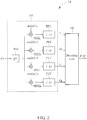
- FIG. 2 is a schematic diagram of the non-orthogonal demodulation module 14 according to an embodiment of the present application.
- the non-orthogonal demodulation module 14 comprises a mixing-and-integrating unit 140 and a decoding unit 142.
- the mixing-and-integrating unit 140 is configured to perform the mixing operations and the integrating operations on the received signal RX at the frequencies f a , f b , to generate in-phase components I a , I b and quadrature components Q a , Q b corresponding to the frequencies f a , f b .
- the decoding unit 142 may generate decoding matrices D I and D Q corresponding to an I-channel and a Q-channel, and compute the energies A 2 , B 2 corresponding to the transmitted signals TX a , TX b according to the decoding matrices D I , D Q , the in-phase components I a , I b and the quadrature components Q a , Q b .
- the decoding unit 142 may be realized by digital circuit or DSP (Digital Signal Processor).
- the circuit structure of the mixing-and-integrating unit 140 is known by people skilled in the art, which is briefed in the following.
- the mixing-and-integrating unit 140 comprises mixers MXI a , MXQ a , MXI b , MXQ b , a window function unit WD and an integrator INT.
- the window function unit WD is equivalent to applying a window function g ( t ) on the received signal RX in a continuous time domain.
- the mixers MXI a , MXQ a , MXI b , MXQ b multipliy the output of the window function unit WD by sin2 ⁇ f a t , cos2 ⁇ f a t , sin2 ⁇ f b t , cos2 ⁇ f b t , respectively.
- the integrator INT performs integration on the outputs of the mixers MXI a , MXQ a , MXI b , MXQ b , and outputs the in-phase components I a , I b and the quadrature components Q a , Q b .
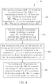
- FIG. 3 is a schematic diagram of a decoding process 30 according to an embodiment of the present application.
- the decoding unit 142 performs the decoding process 30 to compute the energies A 2 , B 2 corresponding to the transmitted signals TX a , TX b .
- the decoding process 30 comprises the following steps: Step 300: Arrange the in-phase components I a , I b as an in-phase vector v I , and arrange the quadrature components Q a , Q b as a quadrature vector v Q .
- Step 302 Obtain a matrix P I and a matrix P Q .
- Step 304 Compute the decoding matrix D I as an inverse matrix of the matrix P I , and compute the decoding matrix D Q as an inverse matrix of the matrix P Q .
- Step 306 Obtain an in-phase result r I and a quadrature result r Q according to the decoding matrices D I , D Q , the in-phase vector v I and the quadrature vector v Q .
- Step 308 Compute the energies A 2 , B 2 corresponding to the transmitted signals TX a , TX b according to the in-phase result r I and the quadrature result r Q .
- Step 302 to Step 308 are described as the following.
- the operations performed by the mixing-and-integrating unit 140 on the received signal RX are linear operations, the amplitudes A, B and the in-phase components I a , I b and the quadrature components Q a , Q b outputted by the mixing-and-integrating unit 140 have linear relationship.
- the amplitude A has a linear relationship versus r I,a , r Q,a ; the amplitude B has a linear relationship versus r I,b , r Q,b .
- the matrices P I and P Q are configured to describe the linear relationships between the in-phase components (I a , I b ), the quadrature components (Q a , Q b ) and r I,a , r Q,a . That is, the matrix P I is configured to described the linear relationship of the in-phase vector v I versus r I ; the matrix P Q is configured to described the linear relationship of the quadrature vector v Q versus r Q .
- the decoding unit 142 obtains the matrix P I and the matrix P Q first.
- a sum spectrum value G ( f a+b ) and a difference spectrum value G ( f a-b ) represent spectrum values of the window spectrum G(f) at the frequency sum f a+b and the frequency difference f a-b , respectively, and G (2 f a ) and G (2 f b ) represent spectrum values of the window spectrum G(f) at a double frequency 2 f a and a double frequency 2 f b .
- Q a ⁇ ⁇ T / 2 T / 2 A sin 2 ⁇
- Ignoring the double frequency spectrum values G ( 2f a ), G (2 f b ), the in-phase components I a , I b and the quadrature components Q a , Q b may be expressed as eq. 2.1-2.4.
- I a AT 2 cos ⁇ a + ⁇ B 2 G f a + b + B 2 G f a ⁇ b cos ⁇ b
- I b ⁇ A 2 G f a + b + A 2 G f a ⁇ b cos ⁇ a + BT 2 cos ⁇ b
- Q a AT 2 sin ⁇ a + B 2 G f a + b + B 2 G f a ⁇ b sin ⁇ b
- Q b A 2 G f a + b + A 2 G f a ⁇ b sin ⁇ a + BT 2 sin ⁇ b
- the in-phase vector v I and the quadrature vector v Q may be expressed in matrix form as eq. 3.1 and 3.2.
- the decoding unit 142 may obtain the matrix P I as eq. 4.1, and may obtain the matrix P Q as eq. 4.2.
- the off-diagonal entries of the matrices P I , P Q are related to the difference spectrum value G ( f a-b ) and the sum spectrum value G ( f a+b ), which means that, the off-diagonal entries of the matrices P I , P Q are related to the frequency difference f a-b and the frequency sum f a+b .
- the decoding unit 142 may compute the in-phase result r I as eq. 5.1, and compute the quadrature result r Q as eq. 5.2.
- the time interval T is known to the decoding unit 142, such that the decoding unit 142 may compute the energies A 2 , B 2 corresponding to the transmitted signals TX a , TX b according to the in-phase result r I and the quadrature result r Q .
- the decoding unit 142 may obtain the matrices P I , P Q as eq. 6 in Step 302, and compute the energies A 2 , B 2 corresponding to the transmitted signals TX a , TX b according to the details of Steps 304-308.
- the decoding unit 142 which only needs one single matrix P in Step 302, to execute the following Steps 304-308, and the off-diagonal entries of the matrix P are related to the difference spectrum value G ( f a-b ). That is, the off-diagonal entries of the matrix P are related to the frequency difference f a-b .
- the matrices P I , P Q may be expressed as eq. 7.1-7.2 (by ignoring the double frequency spectrum values), eq. 8 (by ignoring the double frequency spectrum values and the sum spectrum value) or eq.
- the signal generating module 12 of the touch system 10 may transmit the transmitted signals TX a , TX b to the two transmitting electrodes TE1, TE3 at the same time, the non-orthogonal demodulation module 14 receives the received signal RX at the receiving electrode RE2, and the mixing-and-integrating unit 140 generates the in-phase components I a , I b and the quadrature components Q a , Q b corresponding to the frequencies f a , f b .
- the decoding unit 142 by executing the decoding process 30, obtains the matrices P I , P Q , computes the decoding matrices D I , D Q as the inverse matrices of the matrices P I , P Q , respectively, and computes the energies A 2 , B 2 corresponding to the transmitted signals TX a , TX b according to the decoding matrices D I , D Q .
- Operations of the touch system 10 may be summarized into a non-orthogonal demodulation process. Please refer to FIG. 4.
- FIG. 4 is a schematic diagram of a non-orthogonal demodulation process 40 according to an embodiment of the present application.
- the non-orthogonal demodulation process 40 is executed by the touch system 10, which comprises the following steps: Step 400: The signal generating module 12 transmits the transmitted signals TX a , TX b to the transmitting electrodes TE1, TE3 in a first time, wherein the transmitted signals TX a , TX b are corresponding to the frequencies f a , f b , and the transmitted signals TX a , TX b are not orthogonal to each other.
- Step 402 The non-orthogonal demodulation module 14 receives the received signal RX from the receiving electrode RE2 within the receiving electrodes RE1-REN in the first time.
- Step 404 The mixing-and-integrating unit 140 performs the mixing operations and the integrating operations on the received signal RX respectively at the frequencies f a , f b , so as to generate the in-phase components I a , I b and the quadrature components Q a , Q b corresponding to the frequencies f a , f b .
- Step 406 The decoding unit 142 generates the decoding matrices D I , D Q , and computes the energies A 2 , B 2 corresponding to the transmitted signals TX a , TX b according to the decoding matrices D I , D Q , the in-phase vector v I and the quadrature vector v Q .
- Step 406 Details of Step 406 are introduced in the decoding process 30, and other details of the non-orthogonal demodulation process 40 may be referred to the paragraphs stated in the above, which are not narrated herein for brevity.
- the matrices P I , P Q may be obtained by calibration, which may further fit into the practical situation. That is, the touch system 10 may perform a calibration process, before the non-orthogonal demodulation process 40 is executed, to obtain the matrices P I , P Q , and then execute the non-orthogonal demodulation process 40 based on the matrices P I , P Q derived from the calibration process, so as to obtain the energies A 2 , B 2 corresponding to the transmitted signals TX a , TX b .
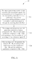
- FIG. 5 is a schematic diagram of a calibration process 50 according to an embodiment of the present application.
- the calibration process 50 is executed by the touch system 10, which comprises the following steps: Step 500: The signal generating module 12 only transmits the transmitted signals TX a corresponding to the frequencies f a to the transmitting electrode TE1 in a calibration time, and the non-orthogonal demodulation module 14 receives a calibration signal CS through the receiving electrode RE2.
- Step 502 The mixing-and-integrating unit 140 generates calibration in-phase components CI a , CI b and calibration quadrature components CQ a , CQ b corresponding to the frequencies f a , f b according to the calibration signal CS.
- Step 504: The decoding unit 142 generates the matrices P I , P Q according to the calibration in-phase components CI a , CI b and the calibration quadrature components CQ a , CQ b .
- the mixing-and-integrating unit 140 may generate the calibration in-phase components CI a , CI b and the calibration quadrature components CQ a , CQ b corresponding to the frequencies f a , f b as eq. 10.1-10.4.
- the window function g ( t ) has the time interval T
- the window spectrum G (f) has zero crossing point at the frequency f which is equal to a multiple of the reciprocal of the time interval T, i.e., G ( f )
- the double frequency spectrum value G (2 f a ) is equal to 0.
- CI a AT 2 cos ⁇ a
- CI b ⁇ A 2 G f a + b + A 2 G f a ⁇ b cos ⁇ a
- CQ a AT 2 sin ⁇ a
- CQ b A 2 G f a + b + A 2 G f a ⁇ b sin ⁇ a
- the decoding unit 142 may obtain the matrices P I , P Q as eq. 11.1 and eq. 11.2.
- P I 1 CI b / CI a CI b / CI a 1
- P Q 1 CQ b / CQ a CQ b / CQ a 1
- the embodiments in the above transmit two single-tone transmitted signals TX a , TX b to two transmitting electrodes at one time, which is not limited thereto.
- the signal generating module 12 may transmit the plurality of transmitted signals to the plurality of transmitting electrodes at one (the same) time.
- the signal generating module 12 may transmit TX a , TX b , TX d , TX d to four transmitting electrodes at one (the same) time.
- A, B, C, D are the amplitudes corresponding to the transmitted signals TX a , TX b , TX d , TX d perceived at the receiving electrode
- a 2 , B 2 , C 2 , D 2 are the energies corresponding to the transmitted signals TX a , TX b , TX d , TX d at the receiving electrodes.
- the in-phase components I a , I b , I d , I d and the quadrature components Q a , Q b , Q c , Q d corresponding to the frequencies f a , f b , f e , f d may be expressed as eq. 12.1-12.8, where the double frequency spectrum values and the sum spectrum values are ignored.
- the in-phase vector v I and the quadrature vector v Q may be expressed in matrix form as eq. 13.1-13.2.
- the matrices P I , P Q may be expressed as eq. 14.
- the off-diagonal entries of the matrices P I , P Q are related to the difference spectrum values G ( f a-b ), G ( f a-c ), G ( f a-d ), G ( f b-c ) , G ( f b-d ), G ( f c-d ). That is, the off-diagonal entries of the matrix P are related to the frequency difference f a-b , f a-c , f a-d , f b-c , f b-d , f c-d . That is also within the scope of the present application.
- I a AT 2 cos ⁇ a + B 2 G f a ⁇ b cos ⁇ b + C 2 G f a ⁇ c cos ⁇ c + D 2 G f a ⁇ d cos ⁇ d
- I b A 2 G f a ⁇ b cos ⁇ a + BT 2 cos ⁇ b + C 2 G f b ⁇ c cos ⁇ c + D 2 G f b ⁇ d cos ⁇ d
- I c A 2 G f a ⁇ c cos ⁇ a + B 2 G f b ⁇ c cos ⁇ b + CT 2 cos ⁇ c + D 2 G f c ⁇ d cos ⁇ d
- I d A 2 G f a ⁇ d cos ⁇ a + B 2 G f b ⁇ d cos ⁇ b + C 2 G f c ⁇ d cos ⁇ d
- Q A 2 G f a
- the present application utilizes the decoding matrices to perform demodulation on the non-orthogonal transmitted signals, to compute the energies corresponding to the plurality of transmitted signals and to determine the coordinate of the touch event.
- the present application has advantages of having smaller signal band.
Landscapes
- Engineering & Computer Science (AREA)
- General Engineering & Computer Science (AREA)
- Theoretical Computer Science (AREA)
- Human Computer Interaction (AREA)
- Physics & Mathematics (AREA)
- General Physics & Mathematics (AREA)
- Computer Networks & Wireless Communication (AREA)
- Signal Processing (AREA)
- Digital Transmission Methods That Use Modulated Carrier Waves (AREA)
Abstract
Description
- The present application relates to a non-orthogonal demodulation module, a touch system and a non-orthogonal demodulation method, and more particularly, to a non-orthogonal demodulation module, a touch system and a non-orthogonal demodulation method reducing signal band.
- As the technology evolves, the operating interfaces of various electronic products gradually become more user-friendly in recent years. For example, through the touch panel, the user can directly operate on the screen with a finger or a stylus to input a message/text/pattern, which spares the trouble of using an input device such as a keyboard or a button. In fact, the touch panel usually includes a sensing panel and a monitor disposed behind the sensing panel. The electronic device determines the meaning of the touch events according to the location of the touch made by the user on the sensing panel and the content displayed by the monitor, and performs the corresponding operations.
- The touch technology in the prior art has developed a method of transmitting signals, which have different frequencies and are mutually orthogonal, by two transmitting electrodes of the touch system at the same time (i.e., transmitting two signals to two electrodes) . Since the transmitted signals are mutually orthogonal, signals at different frequencies can be differentiated in the demodulation process.
FIG. 6 illustrates signal spectrums of two orthogonal signals, and frequencies of which are fa and fb . To maintain the orthogonality, the frequencies of the two orthogonal signals have to be separated by a specific frequency gap. However, if two or more orthogonal signals are transmitted, the bandwidth occupied by the signals (a.k.a., signal band) would be large, and no interference with the signal band has to be guaranteed, which complicates design of the touch system. - Therefore, how to reduce the signal band when multiple signals is transmitted to multiple electrodes is a significant objective in the field.
- It is therefore an objective of an embodiment of the present application to provide a non-orthogonal demodulation module, a touch system and a non-orthogonal demodulation method reducing the signal band, to improve over disadvantages of the prior art.
- To solve the technical problem stated in the above, an embodiment of the present application provides a non-orthogonal demodulation module to perform demodulation on a received signal. The received signal is related to a summation of a plurality of transmitted signals, the plurality of transmitted signals are corresponding to a plurality of frequencies, and the plurality of transmitted signals are not orthogonal to each other, the non-orthogonal demodulation module comprising a mixing-and-integrating unit, configured to perform mixing operations and integrating operations on the received signal respectively at the plurality of frequencies, to generate a plurality of in-phase components and a plurality of quadrature components corresponding to the plurality of frequencies; and a decoding unit, configured to generate at least a decoding matrix, and compute a plurality of energies corresponding to the plurality of transmitted signals according to the at least a decoding matrix, the plurality of in-phase components and the plurality of quadrature components.
- For example, the decoding unit is configured to perform the following steps: arranging the plurality of in-phase components as an in-phase vector, and arranging the plurality of quadrature components as a quadrature vector; obtaining at least a matrix, wherein the at least a matrix comprises a plurality of off-diagonal entries, the plurality of off-diagonal entries is related to the at least a frequency difference, and the at least a frequency difference is a frequency difference between two frequencies within the plurality of frequencies; computing the at least a decoding matrix, wherein the at least a decoding matrix is proportional to in inverse matrix of the at least a matrix; obtaining an in-phase result and a quadrature result according to the at least a decoding matrix, the in-phase vector and the quadrature vector; and computing the plurality of energies corresponding to the plurality of transmitted signals according to the in-phase result and the quadrature result.
- For example, the plurality of off-diagonal entries is related to the at least a frequency difference and at least a frequency sum, and the at least a frequency sum is a frequency sum of two frequencies within the plurality of frequencies.
- For example, the mixing-and-integrating unit applies a window function on the received signal, the window function corresponds to a window spectrum, the plurality of off-diagonal entries is related to at least a difference spectrum value, and the at least a difference spectrum value is a spectrum value of the window spectrum corresponding to the at least a frequency difference.
- For example, the plurality of off-diagonal entries is related to the at least a difference spectrum value and at least a sum spectrum value, the at least a sum spectrum value is a spectrum value of the window spectrum corresponding to at least a frequency sum, and the at least a frequency sum is a frequency sum of two frequencies within the plurality of frequencies.
- To solve the technical problem stated in the above, an embodiment of the present application provides a touch system, comprising a plurality of transmitting electrodes; a plurality of receiving electrodes; a signal generating module, coupled to the plurality of transmitting electrodes, wherein in a first time, the signal generating module transmits the plurality of transmitted signals respectively to the plurality of transmitting electrodes, the plurality of transmitted signals are corresponding to a plurality of frequencies, and the plurality of transmitted signals are not orthogonal to each other; and a non-orthogonal demodulation module, coupled to the plurality of transmitting electrodes, wherein in the first time, the non-orthogonal demodulation module receives a received signal on a first receiving electrode within the plurality of receiving electrodes, the non-orthogonal demodulation module comprising a mixing-and-integrating unit, configured to perform mixing operations and integrating operations on the received signal respectively at the plurality of frequencies, to generate a plurality of in-phase components and a plurality of quadrature components corresponding to the plurality of frequencies; and a decoding unit, configured to generate at least a decoding matrix, and computing a plurality of energies corresponding to the plurality of transmitted signals according to the at least a decoding matrix, the plurality of in-phase components and the plurality of quadrature components.
- For example, the signal generating module transmits a first transmitted signal to a first transmitting electrode within the plurality of transmitting electrodes in a calibration time, the non-orthogonal demodulation module receives a calibration signal through the first receiving electrode, the mixing-and-integrating unit generates a plurality of calibration in-phase components and a plurality of calibration quadrature components corresponding to the plurality of frequencies according to the calibration signal, the decoding unit generates the at least a matrix according to the plurality of calibration in-phase components or the calibration quadrature components, and the first transmitted signal is corresponding to a first frequency within the plurality of frequencies.
- For example, an off-diagonal entry within the plurality of off-diagonal entries is a ratio of a first calibration in-phase component and a second calibration in-phase component within the plurality of calibration in-phase components, and the first calibration in-phase component is corresponding to the first frequency.
- For example, an off-diagonal entry within the plurality of off-diagonal entries is a ratio of a first calibration quadrature component and a second calibration quadrature component within the plurality of calibration quadrature components, and the first calibration quadrature component is corresponding to the first frequency.
- For example, the first frequency times a time interval is an integer, and the time interval is a window function interval of the window function or an integration interval of the integrating operation.
- To solve the technical problem stated in the above, an embodiment of the present application provides a non-orthogonal demodulation method, applied in a touch system. The touch system comprises a plurality of transmitting electrodes and a plurality of receiving electrodes. The non-orthogonal demodulation method comprises transmitting the plurality of transmitted signals respectively to the plurality of transmitting electrodes in a first time, wherein the plurality of transmitted signals are corresponding to a plurality of frequencies, and the plurality of transmitted signals are not orthogonal to each other; receiving a received signal from a first receiving electrode within the plurality of receiving electrodes in the first time; performing mixing operations and integrating operations on the received signal respectively at the plurality of frequencies, to generate a plurality of in-phase components and a plurality of quadrature components corresponding to the plurality of frequencies; and generating at least a decoding matrix, and computing a plurality of energies corresponding to the plurality of transmitted signals according to the at least a decoding matrix, the plurality of in-phase components and the plurality of quadrature components.
- The embodiments of the present application utilizes the decoding matrices to perform demodulation on the non-orthogonal transmitted signals, to compute the energies corresponding to the plurality of transmitted signals and to determine the coordinate of the touch event. Compared to the prior art, the present application has advantages of having smaller signal band.
These and other objectives of the present invention will no doubt become obvious to those of ordinary skill in the art after reading the following detailed description of the preferred embodiment that is illustrated in the various figures and drawings. -
-
FIG. 1 is a schematic diagram of a touch system according to an embodiment of the present application; -
FIG. 2 is a schematic diagram of a non-orthogonal demodulation module according to an embodiment of the present application; -
FIG. 3 is a schematic diagram of a decoding process according to an embodiment of the present application; -
FIG. 4 is a schematic diagram of a touch process according to an embodiment of the present application; -
FIG. 5 is a schematic diagram of a calibration process according to an embodiment of the present application; -
FIG. 6 illustrates spectrums of two signals orthogonal to each other. - In order to make the objects, technical solutions and advantages of the present application become more apparent, the following relies on the accompanying drawings and embodiments to describe the present application in further detail. It should be understood that the specific embodiments described herein are only for explaining the present application and are not intended to limit the present application.
- Please refer to
FIG. 1. FIG. 1 is a schematic diagram of atouch system 10 according to an embodiment of the present application. Thetouch system 10 comprises transmitting electrodes TE1-TEM, receiving electrodes RE1-REN, asignal generating module 12 and anon-orthogonal demodulation module 14. Thesignal generating module 12 is coupled to the transmitting electrodes TE1-TEM. The signal generatingmodule 12 may transmit the plurality of transmitted signals respectively to a part or all of the transmitting electrodes TE1-TEM at the same time. Thenon-orthogonal demodulation module 14 is coupled to the transmitting electrodes TE1-TEM. Thenon-orthogonal demodulation module 14 may receive one received signal on one receiving electrode at one time, and perform non-orthogonal demodulation on the received signal, to obtain amplitudes/energies corresponding to the plurality of transmitted signals on the receiving electrode, so as to determine a coordinate of a touch event. Since obtaining the amplitudes of the plurality of transmitted signals is equivalent to obtaining the energies of the plurality of transmitted signals, since obtaining the energies would lead to obtaining the amplitudes, and vice versa. In the following description and claims, it would illustratively be based on obtaining the energies of the plurality of transmitted signals. - In addition, in order to reduce the spectrum band of the plurality of transmitted signals (i.e., reduce the signal band), the plurality of transmitted signals may not be mutually orthogonal to each other. The plurality of transmitted signals may be a plurality of single-tone signals, where the plurality of single-tone signals are corresponding to a plurality of frequencies. For example, by ignoring the phases therein, the transmitted signal TXm may be proportional to sin2πfmt or cos2πfmt, i.e., the transmitted signal TXm is corresponding to the frequency fm . Supposed that the plurality of transmitted signals are all single-tone signals, if a difference between the frequencies fm , fn of two single-tone transmitted signals TXm, TXn is equal to a multiple of a reciprocal of a time interval T (i.e., | fm-fn | =K/T, where K is a positive integer), the single-tone transmitted signals TXm, TXn are orthogonal to each other. On the contrary, if the difference between the frequencies fm, fn is less than 1/T (or not equal to K/T), the single-tone transmitted signals TXm, TXn are not orthogonal to each other. Moreover, the time interval T may be a window function interval or an integration interval, which will be described later on.
- For illustrative purpose, the following description would be based on an illustrative scenario of "the signal generating
module 12 transmitting two single-tone transmitted signals TXa, TXb to two transmitting electrodes TE1, TE3 at the same time (i.e., the first time) and thenon-orthogonal demodulation module 14 receiving the received signal RX on the receiving electrode RE2", but not limited thereto. Supposed that the two single-tone transmitted signals are TXa = sin2πfat and TXb = sin2πfbt, the received signal RX may be expressed as RX=Asin (2πfat+θa ) +Bsin (2πfbt+θb ). θa, θb are phases corresponding to the transmitted signals TXa, TXb received at the receiving electrode RE2, respectively. A, B are amplitudes corresponding to the transmitted signals TXa, TXb received at the receiving electrode RE2, respectively. A2, B2 are energies corresponding to the transmitted signals TXa, TXb received at the receiving electrode RE2, respectively. Thenon-orthogonal demodulation module 14 may derive the energies A2, B2 corresponding to the transmitted signals TXa, TXb according to the received signal RX. - Specifically, please refer to
FIG. 2. FIG. 2 is a schematic diagram of thenon-orthogonal demodulation module 14 according to an embodiment of the present application. Thenon-orthogonal demodulation module 14 comprises a mixing-and-integratingunit 140 and adecoding unit 142. The mixing-and-integratingunit 140 is configured to perform the mixing operations and the integrating operations on the received signal RX at the frequencies fa, fb, to generate in-phase components Ia, Ib and quadrature components Qa, Qb corresponding to the frequencies fa, fb . Thedecoding unit 142 may generate decoding matrices DI and DQ corresponding to an I-channel and a Q-channel, and compute the energies A2, B2 corresponding to the transmitted signals TXa, TXb according to the decoding matrices DI, DQ, the in-phase components Ia, Ib and the quadrature components Qa, Qb. Thedecoding unit 142 may be realized by digital circuit or DSP (Digital Signal Processor). - The circuit structure of the mixing-and-integrating
unit 140 is known by people skilled in the art, which is briefed in the following. The mixing-and-integratingunit 140 comprises mixers MXIa, MXQa, MXIb, MXQb, a window function unit WD and an integrator INT. The window function unit WD is equivalent to applying a window function g(t) on the received signal RX in a continuous time domain. The mixers MXIa, MXQa, MXIb, MXQb multipliy the output of the window function unit WD by sin2πfat, cos2πfat, sin2πfbt, cos2πfbt, respectively. Finally, the integrator INT performs integration on the outputs of the mixers MXIa, MXQa, MXIb, MXQb, and outputs the in-phase components Ia, Ib and the quadrature components Qa, Qb. - Please refer to
FIG. 3. FIG. 3 is a schematic diagram of adecoding process 30 according to an embodiment of the present application. Thedecoding unit 142 performs thedecoding process 30 to compute the energies A2, B2 corresponding to the transmitted signals TXa, TXb. Thedecoding process 30 comprises the following steps:Step 300: Arrange the in-phase components Ia, Ib as an in-phase vector v I, and arrange the quadrature components Qa, Qb as a quadrature vector v Q. Step 302: Obtain a matrix P I and a matrix P Q. Step 304: Compute the decoding matrix D I as an inverse matrix of the matrix P I, and compute the decoding matrix D Q as an inverse matrix of the matrix P Q. Step 306: Obtain an in-phase result r I and a quadrature result r Q according to the decoding matrices D I, D Q, the in-phase vector v I and the quadrature vector v Q. Step 308: Compute the energies A2, B2 corresponding to the transmitted signals TXa, TXb according to the in-phase result r I and the quadrature result r Q. - In
Step 300, thedecoding unit 142 may form the in-phase vector v I as v I =[Ia, Ib] T , and form the quadrature vector v Q as v Q= [Qa, Qb] T . - Principles of
Step 302 to Step 308 are described as the following. In general, since the operations performed by the mixing-and-integratingunit 140 on the received signal RX are linear operations, the amplitudes A, B and the in-phase components Ia, Ib and the quadrature components Qa, Qb outputted by the mixing-and-integratingunit 140 have linear relationship. In vector/matrix form, the in-phase vector v I may be expressed as v I =P I r I, the quadrature vector v Q may be expressed as v Q=P Q r Q, where r I= [rI,a, rI,b] T and r Q= [rQ,a, rQ,b] T. The amplitude A has a linear relationship versus rI,a, rQ,a; the amplitude B has a linear relationship versus rI,b, rQ,b. The matrices P I and P Q are configured to describe the linear relationships between the in-phase components (Ia, Ib), the quadrature components (Qa, Qb) and rI,a, rQ,a. That is, the matrix P I is configured to described the linear relationship of the in-phase vector v I versus rI; the matrix P Q is configured to described the linear relationship of the quadrature vector v Q versus r Q. - In
Step 302, thedecoding unit 142 obtains the matrix P I and the matrix P Q first. InStep 304, thedecoding unit 142 computes the decoding matrix D I to be proportional to the inverse matrix of the matrix P I (i.e., D I=c (P I)-1) and computes the decoding matrix D Q to be proportional to the inverse matrix of the matrix P Q (i.e., D Q=c (P Q)-1), where c is a constant. For brevity, the constant c is assumed to be 1 (c=1), but the constant c is not limited thereto in reality. InStep 306, thedecoding unit 142 may multiply the decoding matrix D I with the in-phase vector v I to obtain the in-phase result r I (i.e., D I v I =r I ), and multiply the decoding matrix D Q with the quadrature vector v Q to obtain the quadrature result r Q (i.e., D Q v Q=r Q). Therefore, inStep 308, thedecoding unit 142 may compute the energies A2, B2 corresponding to the transmitted signals TXa, TXb according to the in-phase result r I and the quadrature result r Q. - In detail, the in-phase components Ia, Ib and the quadrature components Qa, Qb may be expressed as eq. 1.1-1.4 (in the below) . It is assumed that the window function g(t) is 0 when t is less than (-T/2) or greater than T/2, i.e., g(t)=0,∀t∉[-T/2,T/2], where the time interval T may be a window function interval corresponding to the window function g(t) or an integration interval of the integrator. The window function g(t) is corresponding to a window spectrum G(f), and the window spectrum G(f) is Fourier transform of the window function g(t), i.e., G(f) =∫g(t) e-j2πft dt. In addition, a frequency sum fa+b represents a sum of the frequencies fa, fb, which may be expressed as fa+b =fa +fb ; a frequency difference fa-b represents a difference between the frequencies fa, fb, which may be expressed as fa-b =fa -fb . A sum spectrum value G(fa+b ) and a difference spectrum value G(fa-b ) represent spectrum values of the window spectrum G(f) at the frequency sum fa+b and the frequency difference fa-b , respectively, and G(2fa ) and G(2fb ) represent spectrum values of the window spectrum G(f) at a double frequency 2fa and a double frequency 2fb .


- Ignoring the double frequency spectrum values G(2fa ), G(2fb ), the in-phase components Ia, Ib and the quadrature components Qa, Qb may be expressed as eq. 2.1-2.4.


- In other words, the in-phase vector v I and the quadrature vector v Q may be expressed in matrix form as eq. 3.1 and 3.2.


- In an embodiment, in
Step 302, thedecoding unit 142 may obtain the matrix P I as eq. 4.1, and may obtain the matrix P Q as eq. 4.2. InStep 304, thedecoding unit 142 may compute D I= (P I)-1 and D Q = (P Q)-1. As can be seen from eq. 4.1 and 4.2, the off-diagonal entries of the matrices P I, P Q are related to the difference spectrum value G(fa-b ) and the sum spectrum value G(fa+b ), which means that, the off-diagonal entries of the matrices P I, P Q are related to the frequency difference fa-b and the frequency sum fa+b .

- Therefore, in
Step 306, thedecoding unit 142 may compute the in-phase result r I as eq. 5.1, and compute the quadrature result r Q as eq. 5.2.

- According to eq. 3.1, 3.2, rI,a and rI,b within the in-phase result r I are expressed as rI,a= (AT/2) cosθ a and rI,b= (BT/2) cosθb , and rQ,a and rQ,b within the quadrature result r Q are expressed as rQ,a = (AT/2) sinθ a and rQ,b = (BT/2) sinθ b. Therefore, in
Step 308, thedecoding unit 142 may obtain (AT/2)2= (rI,a)2+ (rQ,a)2 and (BT/2)2 = (rI,b)2+ (rQ,b)2. In addition, the time interval T is known to thedecoding unit 142, such that thedecoding unit 142 may compute the energies A2, B2 corresponding to the transmitted signals TXa, TXb according to the in-phase result r I and the quadrature result r Q. - The embodiment stated in the above illustrates obtaining the matrices P I, P Q under the condition of ignoring the double frequency spectrum values G(2fa ), G(2fb ). In another embodiment, the sum spectrum value G(fa+b ) may be further neglected. That is, the
decoding unit 142 may obtain the matrices P I, P Q as eq. 6 inStep 302, and compute the energies A2, B2 corresponding to the transmitted signals TXa, TXb according to the details of Steps 304-308.
- Notably, under the case of ignoring the double frequency spectrum values G(2fa ), G(2fb ) and the sum spectrum value G(fa+b ), it is sufficient for the
decoding unit 142, which only needs one single matrix P inStep 302, to execute the following Steps 304-308, and the off-diagonal entries of the matrix P are related to the difference spectrum value G(fa-b ). That is, the off-diagonal entries of the matrix P are related to the frequency difference fa-b . - For example, the window function g (t) may be a rectangular window. That is, the window function g(t) may be expressed as g(t) =rect (t/T), i.e., g(t)=1,∀t∈[-T/2,T/2], which means that the window function unit WD does not suppress sidelobe of its output signal but only constraint an integration interval of the integrator INT. In this case, the matrices P I, P Q may be expressed as eq. 7.1-7.2 (by ignoring the double frequency spectrum values), eq. 8 (by ignoring the double frequency spectrum values and the sum spectrum value) or eq. 9.1-9.2(holding the double frequency spectrum values and the sum spectrum value), with sinc (x) =sin (πx) / (πx).


- In a short summary, the
signal generating module 12 of thetouch system 10 may transmit the transmitted signals TXa, TXb to the two transmitting electrodes TE1, TE3 at the same time, thenon-orthogonal demodulation module 14 receives the received signal RX at the receiving electrode RE2, and the mixing-and-integratingunit 140 generates the in-phase components Ia, Ib and the quadrature components Qa, Qb corresponding to the frequencies fa, fb . Thedecoding unit 142, by executing thedecoding process 30, obtains the matrices P I, P Q, computes the decoding matrices D I, D Q as the inverse matrices of the matrices P I, P Q, respectively, and computes the energies A2, B2 corresponding to the transmitted signals TXa, TXb according to the decoding matrices D I, D Q. Operations of thetouch system 10 may be summarized into a non-orthogonal demodulation process. Please refer toFIG. 4. FIG. 4 is a schematic diagram of anon-orthogonal demodulation process 40 according to an embodiment of the present application. Thenon-orthogonal demodulation process 40 is executed by thetouch system 10, which comprises the following steps:Step 400: The signal generating module 12 transmits the transmitted signals TXa, TXb to the transmitting electrodes TE1, TE3 in a first time, wherein the transmitted signals TXa, TXb are corresponding to the frequencies fa , fb , and the transmitted signals TXa, TXb are not orthogonal to each other.Step 402: The non-orthogonal demodulation module 14 receives the received signal RX from the receiving electrode RE2 within the receiving electrodes RE1-REN in the first time.Step 404: The mixing-and-integrating unit 140 performs the mixing operations and the integrating operations on the received signal RX respectively at the frequencies fa , fb , so as to generate the in-phase components Ia, Ib and the quadrature components Qa, Qb corresponding to the frequencies fa , fb .Step 406: The decoding unit 142 generates the decoding matrices D I, D Q, and computes the energies A2, B2 corresponding to the transmitted signals TXa, TXb according to the decoding matrices D I, D Q, the in-phase vector v I and the quadrature vector v Q. - Details of
Step 406 are introduced in thedecoding process 30, and other details of thenon-orthogonal demodulation process 40 may be referred to the paragraphs stated in the above, which are not narrated herein for brevity. - Furthermore, in practice, there may be other channel effect between the
signal generating module 12 and thenon-orthogonal demodulation module 14. Thus, in an embodiment, the matrices P I, P Q may be obtained by calibration, which may further fit into the practical situation. That is, thetouch system 10 may perform a calibration process, before thenon-orthogonal demodulation process 40 is executed, to obtain the matrices P I, P Q, and then execute thenon-orthogonal demodulation process 40 based on the matrices P I, P Q derived from the calibration process, so as to obtain the energies A2, B2 corresponding to the transmitted signals TXa, TXb. - Specifically, please refer to
FIG. 5. FIG. 5 is a schematic diagram of acalibration process 50 according to an embodiment of the present application. Thecalibration process 50 is executed by thetouch system 10, which comprises the following steps:Step 500: The signal generating module 12 only transmits the transmitted signals TXa corresponding to the frequencies fa to the transmitting electrode TE1 in a calibration time, and thenon-orthogonal demodulation module 14 receives a calibration signal CS through the receiving electrode RE2.Step 502: The mixing-and-integrating unit 140 generates calibration in-phase components CIa, CIb and calibration quadrature components CQa, CQb corresponding to the frequencies fa , fb according to the calibration signal CS.Step 504: The decoding unit 142 generates the matrices P I, P Q according to the calibration in-phase components CIa, CIb and the calibration quadrature components CQa, CQb. - In
Step 500, thesignal generating module 12 only transmits the transmitted signal TXa corresponding to the frequency fa to the transmitting electrode TE1 (where the transmitted signal TXa may be expressed as TXa=sin2πfat) in the calibration time, where the calibration time is before the first time. The calibration signal CS received by thenon-orthogonal demodulation module 14 through the receiving electrode RE2 in the calibration time may be expressed as CS=Asin (2πfat+θa ). In addition, the frequency fa may be chosen as a multiple to the reciprocal of the time interval T, i.e., fa =K/T, which means that the frequency fa times the time interval T would be an integer. - In
Step 502, according to the calibration signal CS, the mixing-and-integratingunit 140 may generate the calibration in-phase components CIa, CIb and the calibration quadrature components CQa, CQb corresponding to the frequencies fa, fb as eq. 10.1-10.4. Notably, since the window function g(t) has the time interval T, the window spectrum G(f) has zero crossing point at the frequency f which is equal to a multiple of the reciprocal of the time interval T, i.e., G(f) | f=K/T=0. In other words, when the frequency fa is a multiple of the reciprocal of the time interval T, the double frequency spectrum value G(2fa ) is equal to 0.


- Therefore, in
Step 504, thedecoding unit 142 may obtain the matrices P I, P Q as eq. 11.1 and eq. 11.2.

- In other words, by the
calibration process 50, thetouch system 10 may only transmit the transmitted signal TXa=sin2πfat to the transmitting electrode TE1, obtain the calibration in-phase components CIa, CIb and the calibration quadrature components CQa, CQb in the calibration time, and accordingly obtain P I, P Q by eq. 11.1 and 11.2. Therefore, thetouch system 10 may utilize the matrices P I, P Q (as eq. 11.1, 11.2) derived from thecalibration process 50 to execute the non-orthogonal demodulation process 40 (or the decoding process 30), so as to obtain the energies A2, B2 corresponding to the transmitted signals TXa, TXb. - Notably, the embodiments stated in the above are utilized for illustrating the concept of the present application. Those skilled in the art may make modifications and alterations accordingly, and not limited herein. For example, the embodiments in the above transmit two single-tone transmitted signals TXa, TXb to two transmitting electrodes at one time, which is not limited thereto. The
signal generating module 12 may transmit the plurality of transmitted signals to the plurality of transmitting electrodes at one (the same) time. For example, thesignal generating module 12 may transmit TXa, TXb, TXd, TXd to four transmitting electrodes at one (the same) time. The received signal RX may be expressed as RX = Asin (2πfat+θa ) + Bsin (2πfbt+θb ) + Csin (2πfct+θc ) + Dsin (2πfdt+θd ). θa, θb, θa, θb corresponding to the transmitted signals TXa, TXb, TXd, TXd perceived at the receiving electrode, A, B, C, D are the amplitudes corresponding to the transmitted signals TXa, TXb, TXd, TXd perceived at the receiving electrode, and A2, B2, C2, D2 are the energies corresponding to the transmitted signals TXa, TXb, TXd, TXd at the receiving electrodes. The in-phase components Ia, Ib, Id, Id and the quadrature components Qa, Qb, Qc, Qd corresponding to the frequencies fa, fb, fe, fd may be expressed as eq. 12.1-12.8, where the double frequency spectrum values and the sum spectrum values are ignored. The frequency difference fx-y represents a difference between the frequencies fx, fy, which may be expressed as fx-y =fx -fy . The in-phase vector v I and the quadrature vector v Q may be expressed in matrix form as eq. 13.1-13.2. The matrices P I, P Q may be expressed as eq. 14. Notably, the off-diagonal entries of the matrices P I, P Q are related to the difference spectrum values G(fa-b ), G(fa-c ), G(fa-d ), G(fb-c ), G(fb-d ), G(fc-d ). That is, the off-diagonal entries of the matrix P are related to the frequency difference fa-b , fa-c , fa-d , fb-c , fb-d , fc-d . That is also within the scope of the present application.


- In summary, the present application utilizes the decoding matrices to perform demodulation on the non-orthogonal transmitted signals, to compute the energies corresponding to the plurality of transmitted signals and to determine the coordinate of the touch event. Compared to the prior art, the present application has advantages of having smaller signal band.
- The foregoing is only embodiments of the present application, which is not intended to limit the present application. Any modification following principle of the present application, equivalent substitutions, improvements should be included within the scope of the present application.
Claims (18)
- A non-orthogonal demodulation module, configured to perform demodulation on a received signal, wherein the received signal is related to a summation of a plurality of transmitted signals, the plurality of transmitted signals are respectively corresponding to a plurality of frequencies, and the plurality of transmitted signals are not orthogonal to each other, characterized by, the non-orthogonal demodulation module comprising:a mixing-and-integrating unit, configured to perform mixing operations and integrating operations on the received signal respectively at the plurality of frequencies, to generate a plurality of in-phase components and a plurality of quadrature components corresponding to the plurality of frequencies; anda decoding unit, configured to generate at least a decoding matrix, and compute a plurality of energies corresponding to the plurality of transmitted signals according to the at least a decoding matrix, the plurality of in-phase components and the plurality of quadrature components.
- The non-orthogonal demodulation module of claim 1, characterized in that, the decoding unit is configured to perform the following steps:arranging the plurality of in-phase components as an in-phase vector, and arranging the plurality of quadrature components as a quadrature vector;obtaining at least a matrix, wherein the at least a matrix comprises a plurality of off-diagonal entries, the plurality of off-diagonal entries is related to at least a frequency difference, and the at least a frequency difference is a frequency difference between two frequencies within the plurality of frequencies;computing the at least a decoding matrix, wherein the at least a decoding matrix is related to an inverse matrix of the at least a matrix;obtaining an in-phase result and a quadrature result according to the at least a decoding matrix, the in-phase vector and the quadrature vector; andcomputing the plurality of energies corresponding to the plurality of transmitted signals according to the in-phase result and the quadrature result.
- The non-orthogonal demodulation module of claim 2, characterized in that, the plurality of off-diagonal entries is related to the at least a frequency difference and at least a frequency sum, and the at least a frequency sum is a frequency sum of two frequencies within the plurality of frequencies.
- The non-orthogonal demodulation module of claim 2, characterized in that, the mixing-and-integrating unit applies a window function on the received signal, the window function corresponds to a window spectrum, the plurality of off-diagonal entries is related to at least a difference spectrum value, and the at least a difference spectrum value is a spectrum value of the window spectrum corresponding to the at least a frequency difference.
- The non-orthogonal demodulation module of claim 4, characterized in that, the plurality of off-diagonal entries is related to the at least a difference spectrum value and at least a sum spectrum value, the at least a sum spectrum value is a spectrum value of the window spectrum corresponding to at least a frequency sum, and the at least a frequency sum is a frequency sum of two frequencies within the plurality of frequencies.
- A touch system, characterized by, comprising:a plurality of transmitting electrodes;a plurality of receiving electrodes;a signal generating module, coupled to the plurality of transmitting electrodes, wherein the signal generating module transmits the plurality of transmitted signals respectively to the plurality of transmitting electrodes in a first time, the plurality of transmitted signals are corresponding to a plurality of frequencies, and the plurality of transmitted signals are not orthogonal to each other; anda non-orthogonal demodulation module, coupled to the plurality of transmitting electrodes, wherein the non-orthogonal demodulation module receives a received signal on a first receiving electrode within the plurality of receiving electrodes in the first time;wherein the orthogonal demodulation module is the non-orthogonal demodulation module of any of claims 1-5.
- The touch system of claim 6, characterized in that, the signal generating module transmits a first transmitted signal to a first transmitting electrode within the plurality of transmitting electrodes in a calibration time, the non-orthogonal demodulation module receives a calibration signal through the first receiving electrode, the mixing-and-integrating unit generates a plurality of calibration in-phase components and a plurality of calibration quadrature components corresponding to the plurality of frequencies according to the calibration signal, the decoding unit generates the at least a matrix according to the plurality of calibration in-phase components or the calibration quadrature components, and the first transmitted signal is corresponding to a first frequency within the plurality of frequencies.
- The touch system of claim 7, characterized in that, an off-diagonal entry within the plurality of off-diagonal entries is a ratio of a first calibration in-phase component and a second calibration in-phase component within the plurality of calibration in-phase components, and the first calibration in-phase component is corresponding to the first frequency.
- The touch system of claim 7, characterized in that, an off-diagonal entry within the plurality of off-diagonal entries is a ratio of a first calibration quadrature component and a second calibration quadrature component within the plurality of calibration quadrature components, and the first calibration quadrature component is corresponding to the first frequency.
- The touch system of claim 7, characterized in that, the first frequency times a time interval is an integer, and the time interval is a window function interval of the window function or an integration interval of the integrating operation.
- A non-orthogonal demodulation method, applied in a touch system, wherein the touch system comprises a plurality of transmitting electrodes and a plurality of receiving electrodes, characterized by, the non-orthogonal demodulation method comprising:transmitting the plurality of transmitted signals respectively to the plurality of transmitting electrodes in a first time, wherein the plurality of transmitted signals are corresponding to a plurality of frequencies, and the plurality of transmitted signals are not orthogonal to each other;receiving a received signal from a first receiving electrode within the plurality of receiving electrodes in the first time;performing mixing operations and integrating operations on the received signal respectively at the plurality of frequencies, to generate a plurality of in-phase components and a plurality of quadrature components corresponding to the plurality of frequencies; andgenerating at least a decoding matrix, and computing a plurality of energies corresponding to the plurality of transmitted signals according to the at least a decoding matrix, the plurality of in-phase components and the plurality of quadrature components.
- The non-orthogonal demodulation method of claim 11, characterized in that, the step of generating the at least a decoding matrix and computing the plurality of energies corresponding to the plurality of transmitted signals according to the at least a decoding matrix, the plurality of in-phase components and the plurality of quadrature components comprises:arranging the plurality of in-phase components as an in-phase vector, and arranging the plurality of quadrature components as a quadrature vector;obtaining at least a matrix, wherein the at least a matrix comprises a plurality of off-diagonal entries, the plurality of off-diagonal entries is related to at least a frequency difference, and the at least a frequency difference is a frequency difference between two frequencies within the plurality of frequencies;computing the at least a decoding matrix, wherein the at least a decoding matrix is proportional to in inverse matrix of the at least a matrix;obtaining an in-phase result and a quadrature result according to the at least a decoding matrix, the in-phase vector and the quadrature vector; andcomputing the plurality of energies corresponding to the plurality of transmitted signals according to the in-phase result and the quadrature result.
- The non-orthogonal demodulation method of claim 12, characterized in that, the plurality of off-diagonal entries is related to the at least a frequency difference and at least a frequency sum, and the at least a frequency sum is a frequency sum of two frequencies within the plurality of frequencies.
- The non-orthogonal demodulation method of claim 12, characterized in that, the plurality of off-diagonal entries is related to at least a difference spectrum value, and the at least a difference spectrum value is a spectrum value of a window spectrum corresponding to the at least a frequency difference.
- The non-orthogonal demodulation method of claim 14, characterized in that, the plurality of off-diagonal entries is related to the at least a difference spectrum value and at least a sum spectrum value, the at least a sum spectrum value is a spectrum value of the window spectrum corresponding to at least a frequency sum, and the at least a frequency sum is a frequency sum of two frequencies within the plurality of frequencies.
- The non-orthogonal demodulation method of claim 12, characterized by, further comprising:in a calibration time, transmitting a first transmitted signal to a first transmitting electrode within the plurality of transmitting electrodes, wherein the first transmitted signal is corresponding to a first frequency within the plurality of frequencies;receiving a calibration signal from the first receiving electrode;generating a plurality of calibration in-phase components and a plurality of calibration quadrature components corresponding to the plurality of frequencies according to the calibration signal; andgenerating the at least a matrix according to the plurality of calibration in-phase components or the calibration quadrature components.
- The non-orthogonal demodulation method of claim 16, characterized by, further comprising:obtaining an off-diagonal entry within the plurality of off-diagonal entries as a ratio of a first calibration in-phase component and a second calibration in-phase component within the plurality of calibration in-phase components, wherein the first calibration in-phase component is corresponding to the first frequency.
- The non-orthogonal demodulation method of claim 16, characterized by, further comprising:
obtaining an off-diagonal entry within the plurality of off-diagonal entries as a ratio of a first calibration quadrature component and a second calibration quadrature component within the plurality of calibration quadrature components, wherein the first calibration quadrature component is corresponding to the first frequency.
Applications Claiming Priority (1)
| Application Number | Priority Date | Filing Date | Title |
|---|---|---|---|
| PCT/CN2017/107757 WO2019080026A1 (en) | 2017-10-26 | 2017-10-26 | Non-orthogonal demodulation module, touch-control system and non-orthogonal demodulation method |
Publications (3)
| Publication Number | Publication Date |
|---|---|
| EP3502854A1 true EP3502854A1 (en) | 2019-06-26 |
| EP3502854A4 EP3502854A4 (en) | 2019-08-14 |
| EP3502854B1 EP3502854B1 (en) | 2023-01-18 |
Family
ID=62006120
Family Applications (1)
| Application Number | Title | Priority Date | Filing Date |
|---|---|---|---|
| EP17909664.9A Active EP3502854B1 (en) | 2017-10-26 | 2017-10-26 | Non-orthogonal demodulation module, touch-control system and non-orthogonal demodulation method |
Country Status (4)
| Country | Link |
|---|---|
| US (1) | US10852878B2 (en) |
| EP (1) | EP3502854B1 (en) |
| CN (1) | CN107980114B (en) |
| WO (1) | WO2019080026A1 (en) |
Families Citing this family (3)
| Publication number | Priority date | Publication date | Assignee | Title |
|---|---|---|---|---|
| US12346507B2 (en) * | 2022-01-27 | 2025-07-01 | Novatek Microelectronics Corp. | Stylus control circuit and stylus |
| TWI822174B (en) * | 2022-07-12 | 2023-11-11 | 敦泰電子股份有限公司 | Active stylus receiving circuit and touch panel system using active stylus pen |
| EP4428662A1 (en) * | 2023-03-07 | 2024-09-11 | Nxp B.V. | Touch panel system using modulated signals as drive signals |
Family Cites Families (20)
| Publication number | Priority date | Publication date | Assignee | Title |
|---|---|---|---|---|
| AU2003231522A1 (en) * | 2003-04-30 | 2004-11-23 | Dequn Liang | A multi-modulation transmitting method |
| CN1956356B (en) * | 2005-10-27 | 2011-05-11 | 中兴通讯股份有限公司 | Frequency range distribution and access method capable of flexible using spectrum resource and its system |
| US8592697B2 (en) * | 2008-09-10 | 2013-11-26 | Apple Inc. | Single-chip multi-stimulus sensor controller |
| US9348451B2 (en) * | 2008-09-10 | 2016-05-24 | Apple Inc. | Channel scan architecture for multiple stimulus multi-touch sensor panels |
| US9753586B2 (en) * | 2009-10-08 | 2017-09-05 | 3M Innovative Properties Company | Multi-touch touch device with multiple drive frequencies and maximum likelihood estimation |
| US9686103B2 (en) * | 2012-04-27 | 2017-06-20 | Mediatek Inc. | Method for compensating the frequency dependent phase imbalance |
| US8913021B2 (en) * | 2012-04-30 | 2014-12-16 | Apple Inc. | Capacitance touch near-field—far field switching |
| US20140204053A1 (en) * | 2013-01-22 | 2014-07-24 | Pixart Imaging Inc. | Concurrent driving capacitive touch sensing device and transmission system |
| US20140267143A1 (en) * | 2013-03-15 | 2014-09-18 | Synaptics Incorporated | System and method for a transcapacitive proximity sensing device |
| US20150029136A1 (en) * | 2013-07-29 | 2015-01-29 | Apple Inc. | Superheterodyne pen stimulus signal receiver |
| TW201530375A (en) * | 2014-01-17 | 2015-08-01 | Raydium Semiconductor Corp | Multi-channel sensing system and operating method thereof |
| TWI509533B (en) * | 2014-04-23 | 2015-11-21 | Novatek Microelectronics Corp | Phase compensation method for multi-scan in touch sensing system and phase compensation circuit thereof |
| US9977592B2 (en) * | 2014-10-30 | 2018-05-22 | Mediatek Inc. | Touch rim control method and associated device |
| US9389742B2 (en) * | 2014-12-10 | 2016-07-12 | Pixart Imaging Inc. | Capacitive touch device, capacitive communication device and communication system |
| US10037094B2 (en) * | 2015-10-29 | 2018-07-31 | Novatek Microelectronics Corp. | Carrier touch sensing system capable of performing phase calibration and carrier signal demodulation |
| US20170139536A1 (en) * | 2015-11-13 | 2017-05-18 | Pixart Imaging Inc. | Fdm based capacitive touch system and operating method thereof |
| US9740356B1 (en) * | 2016-02-05 | 2017-08-22 | Pixart Imaging Inc. | Capacitive touch system using differential sensing and operating method thereof |
| CN107219947B (en) * | 2016-03-22 | 2021-08-10 | 原相科技股份有限公司 | Capacitive touch system using frequency division multiplexing and operation method thereof |
| EP3547092A4 (en) * | 2018-02-05 | 2020-02-12 | Shenzhen Goodix Technology Co., Ltd. | TOUCH CONTROL UNIT, DEMODULATION METHOD AND TOUCH CONTROL SYSTEM |
| WO2019237290A1 (en) * | 2018-06-13 | 2019-12-19 | 深圳市汇顶科技股份有限公司 | Noise detection circuit and method, and detection circuit |
-
2017
- 2017-10-26 WO PCT/CN2017/107757 patent/WO2019080026A1/en not_active Ceased
- 2017-10-26 CN CN201780001414.8A patent/CN107980114B/en active Active
- 2017-10-26 EP EP17909664.9A patent/EP3502854B1/en active Active
-
2018
- 2018-11-19 US US16/195,786 patent/US10852878B2/en active Active
Also Published As
| Publication number | Publication date |
|---|---|
| US10852878B2 (en) | 2020-12-01 |
| WO2019080026A1 (en) | 2019-05-02 |
| CN107980114B (en) | 2021-10-26 |
| EP3502854B1 (en) | 2023-01-18 |
| CN107980114A (en) | 2018-05-01 |
| EP3502854A4 (en) | 2019-08-14 |
| US20190129569A1 (en) | 2019-05-02 |
Similar Documents
| Publication | Publication Date | Title |
|---|---|---|
| CN110612508B (en) | Touch controller, demodulation method and touch system | |
| EP3502854B1 (en) | Non-orthogonal demodulation module, touch-control system and non-orthogonal demodulation method | |
| CN103997476B (en) | Signal generating apparatus and method and mobile communication terminal test device and method | |
| US9491029B2 (en) | Devices and methods for reducing signal distortion in I/Q modulation transceivers | |
| US9059879B2 (en) | Test signal generation and application in receivers | |
| CN100431261C (en) | Improved mixer with multiple local oscillators and systems based thereon | |
| Kolumbán et al. | Theory and application of software defined electronics: Design concepts for the next generation of telecommunications and measurement systems | |
| Rondeau | On the GNU radio ecosystem | |
| US9088331B2 (en) | IQ baseband matching calibration technique | |
| CN114444106B (en) | Correlation coefficient acquisition method and device, electronic equipment and storage medium | |
| Ahmadi et al. | Effect of relativistic acceleration on localized two-mode Gaussian quantum states | |
| CN104980388A (en) | Systems and methods for narrowband signal quadrature error correction | |
| JP2017502559A (en) | Method, system and apparatus for phase noise cancellation | |
| Adler et al. | Hermespy: An open-source link-level evaluator for 6g | |
| CN104219186A (en) | An Analog IQ Modulation Error Correction Method Based on IQ Baseband Signal Amplitude Adjustment | |
| US20230163813A1 (en) | Method and Apparatus Including Error Vector Magnitude Definition and Testing for Antenna Ports and Multi-Layer Transmissions | |
| US11003281B2 (en) | Noise detection circuit, noise detection method and detection circuit | |
| Manicka | GNU radio testbed | |
| WO2023231924A1 (en) | Signal sending method, and sending device and receiving device | |
| Gowda et al. | Design & implementation of FM transceiver using raspberry Pi and SDR | |
| CN112703701B (en) | Demodulation reference signal mapping, device, equipment and storage medium thereof | |
| CN102684682A (en) | Frequency divider arrangement and method for providing quadrature output signal | |
| CN115334578B (en) | Terminal interference measurement method, system, electronic device and readable storage medium | |
| CN115087010B (en) | Downlink signal detection method and device for flexible frame structure simulation system | |
| JP2014093738A (en) | Modulation signal analysis device and modulation signal analysis method |
Legal Events
| Date | Code | Title | Description |
|---|---|---|---|
| STAA | Information on the status of an ep patent application or granted ep patent |
Free format text: STATUS: UNKNOWN |
|
| STAA | Information on the status of an ep patent application or granted ep patent |
Free format text: STATUS: THE INTERNATIONAL PUBLICATION HAS BEEN MADE |
|
| PUAI | Public reference made under article 153(3) epc to a published international application that has entered the european phase |
Free format text: ORIGINAL CODE: 0009012 |
|
| STAA | Information on the status of an ep patent application or granted ep patent |
Free format text: STATUS: REQUEST FOR EXAMINATION WAS MADE |
|
| 17P | Request for examination filed |
Effective date: 20181123 |
|
| AK | Designated contracting states |
Kind code of ref document: A1 Designated state(s): AL AT BE BG CH CY CZ DE DK EE ES FI FR GB GR HR HU IE IS IT LI LT LU LV MC MK MT NL NO PL PT RO RS SE SI SK SM TR |
|
| AX | Request for extension of the european patent |
Extension state: BA ME |
|
| A4 | Supplementary search report drawn up and despatched |
Effective date: 20190717 |
|
| RIC1 | Information provided on ipc code assigned before grant |
Ipc: G06F 3/044 20060101ALI20190711BHEP Ipc: G06F 3/041 20060101AFI20190711BHEP Ipc: H03K 9/00 20060101ALI20190711BHEP |
|
| STAA | Information on the status of an ep patent application or granted ep patent |
Free format text: STATUS: EXAMINATION IS IN PROGRESS |
|
| 17Q | First examination report despatched |
Effective date: 20200506 |
|
| DAV | Request for validation of the european patent (deleted) | ||
| DAX | Request for extension of the european patent (deleted) | ||
| REG | Reference to a national code |
Ref country code: DE Ref legal event code: R079 Ref document number: 602017065670 Country of ref document: DE Free format text: PREVIOUS MAIN CLASS: G06F0003044000 Ipc: G06F0003041000 |
|
| GRAP | Despatch of communication of intention to grant a patent |
Free format text: ORIGINAL CODE: EPIDOSNIGR1 |
|
| STAA | Information on the status of an ep patent application or granted ep patent |
Free format text: STATUS: GRANT OF PATENT IS INTENDED |
|
| RIC1 | Information provided on ipc code assigned before grant |
Ipc: H04L 27/38 20060101ALN20220817BHEP Ipc: H04L 27/233 20060101ALN20220817BHEP Ipc: H04L 27/14 20060101ALN20220817BHEP Ipc: H04L 27/22 20060101ALI20220817BHEP Ipc: H03K 9/00 20060101ALI20220817BHEP Ipc: G06F 3/044 20060101ALI20220817BHEP Ipc: G06F 3/041 20060101AFI20220817BHEP |
|
| INTG | Intention to grant announced |
Effective date: 20220909 |
|
| GRAS | Grant fee paid |
Free format text: ORIGINAL CODE: EPIDOSNIGR3 |
|
| GRAA | (expected) grant |
Free format text: ORIGINAL CODE: 0009210 |
|
| STAA | Information on the status of an ep patent application or granted ep patent |
Free format text: STATUS: THE PATENT HAS BEEN GRANTED |
|
| AK | Designated contracting states |
Kind code of ref document: B1 Designated state(s): AL AT BE BG CH CY CZ DE DK EE ES FI FR GB GR HR HU IE IS IT LI LT LU LV MC MK MT NL NO PL PT RO RS SE SI SK SM TR |
|
| REG | Reference to a national code |
Ref country code: GB Ref legal event code: FG4D |
|
| REG | Reference to a national code |
Ref country code: CH Ref legal event code: EP |
|
| REG | Reference to a national code |
Ref country code: DE Ref legal event code: R096 Ref document number: 602017065670 Country of ref document: DE |
|
| REG | Reference to a national code |
Ref country code: AT Ref legal event code: REF Ref document number: 1545053 Country of ref document: AT Kind code of ref document: T Effective date: 20230215 Ref country code: IE Ref legal event code: FG4D |
|
| REG | Reference to a national code |
Ref country code: LT Ref legal event code: MG9D |
|
| REG | Reference to a national code |
Ref country code: NL Ref legal event code: MP Effective date: 20230118 |
|
| REG | Reference to a national code |
Ref country code: AT Ref legal event code: MK05 Ref document number: 1545053 Country of ref document: AT Kind code of ref document: T Effective date: 20230118 |
|
| PG25 | Lapsed in a contracting state [announced via postgrant information from national office to epo] |
Ref country code: NL Free format text: LAPSE BECAUSE OF FAILURE TO SUBMIT A TRANSLATION OF THE DESCRIPTION OR TO PAY THE FEE WITHIN THE PRESCRIBED TIME-LIMIT Effective date: 20230118 |
|
| PG25 | Lapsed in a contracting state [announced via postgrant information from national office to epo] |
Ref country code: RS Free format text: LAPSE BECAUSE OF FAILURE TO SUBMIT A TRANSLATION OF THE DESCRIPTION OR TO PAY THE FEE WITHIN THE PRESCRIBED TIME-LIMIT Effective date: 20230118 Ref country code: PT Free format text: LAPSE BECAUSE OF FAILURE TO SUBMIT A TRANSLATION OF THE DESCRIPTION OR TO PAY THE FEE WITHIN THE PRESCRIBED TIME-LIMIT Effective date: 20230518 Ref country code: NO Free format text: LAPSE BECAUSE OF FAILURE TO SUBMIT A TRANSLATION OF THE DESCRIPTION OR TO PAY THE FEE WITHIN THE PRESCRIBED TIME-LIMIT Effective date: 20230418 Ref country code: LV Free format text: LAPSE BECAUSE OF FAILURE TO SUBMIT A TRANSLATION OF THE DESCRIPTION OR TO PAY THE FEE WITHIN THE PRESCRIBED TIME-LIMIT Effective date: 20230118 Ref country code: LT Free format text: LAPSE BECAUSE OF FAILURE TO SUBMIT A TRANSLATION OF THE DESCRIPTION OR TO PAY THE FEE WITHIN THE PRESCRIBED TIME-LIMIT Effective date: 20230118 Ref country code: HR Free format text: LAPSE BECAUSE OF FAILURE TO SUBMIT A TRANSLATION OF THE DESCRIPTION OR TO PAY THE FEE WITHIN THE PRESCRIBED TIME-LIMIT Effective date: 20230118 Ref country code: ES Free format text: LAPSE BECAUSE OF FAILURE TO SUBMIT A TRANSLATION OF THE DESCRIPTION OR TO PAY THE FEE WITHIN THE PRESCRIBED TIME-LIMIT Effective date: 20230118 Ref country code: AT Free format text: LAPSE BECAUSE OF FAILURE TO SUBMIT A TRANSLATION OF THE DESCRIPTION OR TO PAY THE FEE WITHIN THE PRESCRIBED TIME-LIMIT Effective date: 20230118 |
|
| PG25 | Lapsed in a contracting state [announced via postgrant information from national office to epo] |
Ref country code: SE Free format text: LAPSE BECAUSE OF FAILURE TO SUBMIT A TRANSLATION OF THE DESCRIPTION OR TO PAY THE FEE WITHIN THE PRESCRIBED TIME-LIMIT Effective date: 20230118 Ref country code: PL Free format text: LAPSE BECAUSE OF FAILURE TO SUBMIT A TRANSLATION OF THE DESCRIPTION OR TO PAY THE FEE WITHIN THE PRESCRIBED TIME-LIMIT Effective date: 20230118 Ref country code: IS Free format text: LAPSE BECAUSE OF FAILURE TO SUBMIT A TRANSLATION OF THE DESCRIPTION OR TO PAY THE FEE WITHIN THE PRESCRIBED TIME-LIMIT Effective date: 20230518 Ref country code: GR Free format text: LAPSE BECAUSE OF FAILURE TO SUBMIT A TRANSLATION OF THE DESCRIPTION OR TO PAY THE FEE WITHIN THE PRESCRIBED TIME-LIMIT Effective date: 20230419 Ref country code: FI Free format text: LAPSE BECAUSE OF FAILURE TO SUBMIT A TRANSLATION OF THE DESCRIPTION OR TO PAY THE FEE WITHIN THE PRESCRIBED TIME-LIMIT Effective date: 20230118 |
|
| REG | Reference to a national code |
Ref country code: DE Ref legal event code: R097 Ref document number: 602017065670 Country of ref document: DE |
|
| PG25 | Lapsed in a contracting state [announced via postgrant information from national office to epo] |
Ref country code: SM Free format text: LAPSE BECAUSE OF FAILURE TO SUBMIT A TRANSLATION OF THE DESCRIPTION OR TO PAY THE FEE WITHIN THE PRESCRIBED TIME-LIMIT Effective date: 20230118 Ref country code: RO Free format text: LAPSE BECAUSE OF FAILURE TO SUBMIT A TRANSLATION OF THE DESCRIPTION OR TO PAY THE FEE WITHIN THE PRESCRIBED TIME-LIMIT Effective date: 20230118 Ref country code: EE Free format text: LAPSE BECAUSE OF FAILURE TO SUBMIT A TRANSLATION OF THE DESCRIPTION OR TO PAY THE FEE WITHIN THE PRESCRIBED TIME-LIMIT Effective date: 20230118 Ref country code: DK Free format text: LAPSE BECAUSE OF FAILURE TO SUBMIT A TRANSLATION OF THE DESCRIPTION OR TO PAY THE FEE WITHIN THE PRESCRIBED TIME-LIMIT Effective date: 20230118 Ref country code: CZ Free format text: LAPSE BECAUSE OF FAILURE TO SUBMIT A TRANSLATION OF THE DESCRIPTION OR TO PAY THE FEE WITHIN THE PRESCRIBED TIME-LIMIT Effective date: 20230118 |
|
| PLBE | No opposition filed within time limit |
Free format text: ORIGINAL CODE: 0009261 |
|
| STAA | Information on the status of an ep patent application or granted ep patent |
Free format text: STATUS: NO OPPOSITION FILED WITHIN TIME LIMIT |
|
| PG25 | Lapsed in a contracting state [announced via postgrant information from national office to epo] |
Ref country code: SK Free format text: LAPSE BECAUSE OF FAILURE TO SUBMIT A TRANSLATION OF THE DESCRIPTION OR TO PAY THE FEE WITHIN THE PRESCRIBED TIME-LIMIT Effective date: 20230118 |
|
| 26N | No opposition filed |
Effective date: 20231019 |
|
| PG25 | Lapsed in a contracting state [announced via postgrant information from national office to epo] |
Ref country code: SI Free format text: LAPSE BECAUSE OF FAILURE TO SUBMIT A TRANSLATION OF THE DESCRIPTION OR TO PAY THE FEE WITHIN THE PRESCRIBED TIME-LIMIT Effective date: 20230118 |
|
| PG25 | Lapsed in a contracting state [announced via postgrant information from national office to epo] |
Ref country code: IT Free format text: LAPSE BECAUSE OF FAILURE TO SUBMIT A TRANSLATION OF THE DESCRIPTION OR TO PAY THE FEE WITHIN THE PRESCRIBED TIME-LIMIT Effective date: 20230118 Ref country code: MC Free format text: LAPSE BECAUSE OF FAILURE TO SUBMIT A TRANSLATION OF THE DESCRIPTION OR TO PAY THE FEE WITHIN THE PRESCRIBED TIME-LIMIT Effective date: 20230118 |
|
| REG | Reference to a national code |
Ref country code: CH Ref legal event code: PL |
|
| REG | Reference to a national code |
Ref country code: BE Ref legal event code: MM Effective date: 20231031 |
|
| PG25 | Lapsed in a contracting state [announced via postgrant information from national office to epo] |
Ref country code: LU Free format text: LAPSE BECAUSE OF NON-PAYMENT OF DUE FEES Effective date: 20231026 |
|
| PG25 | Lapsed in a contracting state [announced via postgrant information from national office to epo] |
Ref country code: LU Free format text: LAPSE BECAUSE OF NON-PAYMENT OF DUE FEES Effective date: 20231026 |
|
| PG25 | Lapsed in a contracting state [announced via postgrant information from national office to epo] |
Ref country code: CH Free format text: LAPSE BECAUSE OF NON-PAYMENT OF DUE FEES Effective date: 20231031 |
|
| PG25 | Lapsed in a contracting state [announced via postgrant information from national office to epo] |
Ref country code: FR Free format text: LAPSE BECAUSE OF NON-PAYMENT OF DUE FEES Effective date: 20231031 Ref country code: CH Free format text: LAPSE BECAUSE OF NON-PAYMENT OF DUE FEES Effective date: 20231031 |
|
| PG25 | Lapsed in a contracting state [announced via postgrant information from national office to epo] |
Ref country code: BE Free format text: LAPSE BECAUSE OF NON-PAYMENT OF DUE FEES Effective date: 20231031 |
|
| REG | Reference to a national code |
Ref country code: DE Ref legal event code: R082 Ref document number: 602017065670 Country of ref document: DE Representative=s name: STRAUS, ALEXANDER, DIPL.-CHEM.UNIV. DR.PHIL., DE |
|
| PG25 | Lapsed in a contracting state [announced via postgrant information from national office to epo] |
Ref country code: IE Free format text: LAPSE BECAUSE OF NON-PAYMENT OF DUE FEES Effective date: 20231026 |
|
| PG25 | Lapsed in a contracting state [announced via postgrant information from national office to epo] |
Ref country code: IE Free format text: LAPSE BECAUSE OF NON-PAYMENT OF DUE FEES Effective date: 20231026 |
|
| PG25 | Lapsed in a contracting state [announced via postgrant information from national office to epo] |
Ref country code: BG Free format text: LAPSE BECAUSE OF FAILURE TO SUBMIT A TRANSLATION OF THE DESCRIPTION OR TO PAY THE FEE WITHIN THE PRESCRIBED TIME-LIMIT Effective date: 20230118 |
|
| PG25 | Lapsed in a contracting state [announced via postgrant information from national office to epo] |
Ref country code: BG Free format text: LAPSE BECAUSE OF FAILURE TO SUBMIT A TRANSLATION OF THE DESCRIPTION OR TO PAY THE FEE WITHIN THE PRESCRIBED TIME-LIMIT Effective date: 20230118 |
|
| PG25 | Lapsed in a contracting state [announced via postgrant information from national office to epo] |
Ref country code: CY Free format text: LAPSE BECAUSE OF FAILURE TO SUBMIT A TRANSLATION OF THE DESCRIPTION OR TO PAY THE FEE WITHIN THE PRESCRIBED TIME-LIMIT; INVALID AB INITIO Effective date: 20171026 |
|
| PG25 | Lapsed in a contracting state [announced via postgrant information from national office to epo] |
Ref country code: HU Free format text: LAPSE BECAUSE OF FAILURE TO SUBMIT A TRANSLATION OF THE DESCRIPTION OR TO PAY THE FEE WITHIN THE PRESCRIBED TIME-LIMIT; INVALID AB INITIO Effective date: 20171026 |
|
| PG25 | Lapsed in a contracting state [announced via postgrant information from national office to epo] |
Ref country code: TR Free format text: LAPSE BECAUSE OF FAILURE TO SUBMIT A TRANSLATION OF THE DESCRIPTION OR TO PAY THE FEE WITHIN THE PRESCRIBED TIME-LIMIT Effective date: 20230118 |
|
| PGFP | Annual fee paid to national office [announced via postgrant information from national office to epo] |
Ref country code: DE Payment date: 20251022 Year of fee payment: 9 |
|
| PGFP | Annual fee paid to national office [announced via postgrant information from national office to epo] |
Ref country code: GB Payment date: 20251023 Year of fee payment: 9 |