US9088331B2 - IQ baseband matching calibration technique - Google Patents
IQ baseband matching calibration technique Download PDFInfo
- Publication number
- US9088331B2 US9088331B2 US14/519,463 US201414519463A US9088331B2 US 9088331 B2 US9088331 B2 US 9088331B2 US 201414519463 A US201414519463 A US 201414519463A US 9088331 B2 US9088331 B2 US 9088331B2
- Authority
- US
- United States
- Prior art keywords
- signal
- output
- generation system
- input
- filter
- Prior art date
- Legal status (The legal status is an assumption and is not a legal conclusion. Google has not performed a legal analysis and makes no representation as to the accuracy of the status listed.)
- Active
Links
- 238000000034 method Methods 0.000 title description 83
- 230000007274 generation of a signal involved in cell-cell signaling Effects 0.000 claims abstract description 145
- 230000006735 deficit Effects 0.000 claims abstract description 103
- 239000004020 conductor Substances 0.000 claims abstract description 59
- 238000005259 measurement Methods 0.000 claims description 76
- 230000004044 response Effects 0.000 claims description 63
- 238000012937 correction Methods 0.000 claims description 37
- 230000005540 biological transmission Effects 0.000 claims description 30
- 238000006243 chemical reaction Methods 0.000 claims description 16
- 238000011144 upstream manufacturing Methods 0.000 claims description 3
- 238000012545 processing Methods 0.000 abstract description 8
- 239000003795 chemical substances by application Substances 0.000 abstract 1
- 238000004364 calculation method Methods 0.000 description 11
- 238000012360 testing method Methods 0.000 description 11
- 238000009795 derivation Methods 0.000 description 9
- 230000009471 action Effects 0.000 description 6
- 238000004891 communication Methods 0.000 description 6
- 238000012986 modification Methods 0.000 description 4
- 230000004048 modification Effects 0.000 description 4
- 230000007423 decrease Effects 0.000 description 3
- 238000004088 simulation Methods 0.000 description 3
- 238000003491 array Methods 0.000 description 2
- 230000008901 benefit Effects 0.000 description 2
- 238000013461 design Methods 0.000 description 2
- 230000006870 function Effects 0.000 description 2
- 239000004065 semiconductor Substances 0.000 description 2
- 230000009466 transformation Effects 0.000 description 2
- 238000012935 Averaging Methods 0.000 description 1
- 239000008186 active pharmaceutical agent Substances 0.000 description 1
- 238000004458 analytical method Methods 0.000 description 1
- 230000008859 change Effects 0.000 description 1
- 238000000205 computational method Methods 0.000 description 1
- 230000001419 dependent effect Effects 0.000 description 1
- 238000005516 engineering process Methods 0.000 description 1
- 238000010348 incorporation Methods 0.000 description 1
- 238000013178 mathematical model Methods 0.000 description 1
- 230000007246 mechanism Effects 0.000 description 1
- 230000003287 optical effect Effects 0.000 description 1
- 238000005192 partition Methods 0.000 description 1
- 230000003068 static effect Effects 0.000 description 1
Images


Classifications
-
- H—ELECTRICITY
- H04—ELECTRIC COMMUNICATION TECHNIQUE
- H04B—TRANSMISSION
- H04B1/00—Details of transmission systems, not covered by a single one of groups H04B3/00 - H04B13/00; Details of transmission systems not characterised by the medium used for transmission
- H04B1/06—Receivers
- H04B1/10—Means associated with receiver for limiting or suppressing noise or interference
- H04B1/12—Neutralising, balancing, or compensation arrangements
- H04B1/123—Neutralising, balancing, or compensation arrangements using adaptive balancing or compensation means
-
- H—ELECTRICITY
- H04—ELECTRIC COMMUNICATION TECHNIQUE
- H04B—TRANSMISSION
- H04B1/00—Details of transmission systems, not covered by a single one of groups H04B3/00 - H04B13/00; Details of transmission systems not characterised by the medium used for transmission
- H04B1/06—Receivers
- H04B1/10—Means associated with receiver for limiting or suppressing noise or interference
- H04B1/12—Neutralising, balancing, or compensation arrangements
-
- H—ELECTRICITY
- H04—ELECTRIC COMMUNICATION TECHNIQUE
- H04B—TRANSMISSION
- H04B17/00—Monitoring; Testing
- H04B17/20—Monitoring; Testing of receivers
- H04B17/21—Monitoring; Testing of receivers for calibration; for correcting measurements
-
- H—ELECTRICITY
- H04—ELECTRIC COMMUNICATION TECHNIQUE
- H04B—TRANSMISSION
- H04B17/00—Monitoring; Testing
-
- H—ELECTRICITY
- H04—ELECTRIC COMMUNICATION TECHNIQUE
- H04L—TRANSMISSION OF DIGITAL INFORMATION, e.g. TELEGRAPHIC COMMUNICATION
- H04L27/00—Modulated-carrier systems
- H04L27/32—Carrier systems characterised by combinations of two or more of the types covered by groups H04L27/02, H04L27/10, H04L27/18 or H04L27/26
- H04L27/34—Amplitude- and phase-modulated carrier systems, e.g. quadrature-amplitude modulated carrier systems
- H04L27/36—Modulator circuits; Transmitter circuits
- H04L27/362—Modulation using more than one carrier, e.g. with quadrature carriers, separately amplitude modulated
- H04L27/364—Arrangements for overcoming imperfections in the modulator, e.g. quadrature error or unbalanced I and Q levels
Definitions
- the present invention relates to the field of electronic system calibration, and more particularly to an apparatus and method for measuring I/Q impairments and correcting those impairments for systems coupled in series.
- Quadrature also known as homodyne, direct conversion or zero-IF
- RF architectures convert between a pair of baseband signals (in-phase and quadrature phase) and RF signals.
- VSA vector signal analyzer
- VSG Vector Signal Generator
- VSG Vector Signal Generator
- phase imbalance is also referred to herein as “phase imbalance”.
- phase imbalance is also referred to herein as “phase imbalance”.
- the baseband portion of the design is separated from the RF portion of the design.
- the device In these types of systems where the device is not calibrated together as one system, it becomes important to properly calibrate each subsystem accurately. Often, each subsystem is tested separately for proper operation. In the test use case, it is important to supply properly calibrated baseband signals to the RF DUTs. (DUT is an acronym for “Device Under Test”.) This could be to test an IQ modulator or demodulator, or to test the baseband subsystem.
- the baseband matching has to be measured. This becomes a very difficult measurement to perform given the accuracies that are needed. In fact, the accuracies that are required for image rejections less than ⁇ 60 dB either do not exist or are not specified in the test and measurement market.
- Gain imbalance measurements are much easier to make than the phase measurements.
- input gain matching a common source can be used to measure the amplitude response of each input channel in sequence where the two responses are then subtracted (subtracted in dB, or divided in voltage). The same can be accomplished for output gain matching where each output is applied to a single input of a digitizer in sequence.
- power meters at low frequencies have great amplitude accuracies and therefore two different power meters could be used together. However, these methods do not account for phase matching.
- a method for determining gain and/or phase imbalance of a signal generation system and/or a signal digitizing system may include the following operations.
- the method may include: directing the signal generation system to generate a first vector calibration signal and to transmit a first vector output signal via the first output and the second output based on the first vector calibration signal; and directing the signal digitizing system to capture a first set of vector samples from the first input and second input in response to the transmission of the first vector output signal.
- the method may include: directing the signal generation system to generate a second vector calibration signal and transmit a second vector output signal based on the second vector calibration signal; and directing the signal digitizing system to capture a second set of vector samples from the first input and second input in response to the transmission of the second vector output signal.
- the method may also include computing a measurement of gain and/or phase imbalance of the signal generation system and/or a measurement of gain and/or phase imbalance of the signal digitizing system based on input data including the first set of vector samples and the second set of vector samples.
- the signal generation system may include a single dual-channel waveform generator or two single-channel waveform generators.
- the signal digitizing system may include a single dual-channel waveform digitizer or two single-channel waveform digitizers.
- a computer system for determining gain and/or phase imbalance of a signal generation system and/or a signal digitizing system may include a processor and memory.
- the signal generation system includes a first output and a second output, and the signal digitizing system includes a first input and a second input.
- the memory stores program instructions, where the program instructions, when executed by the processor, cause the processor to perform the following operations.
- the processor In response to a first signal indicating that a first connection configuration has been achieved between the first and second outputs of the signal generation system and the first and second inputs of the signal digitizing system, the processor directs the signal generation system to generate a first vector calibration signal and transmit a first vector output signal via the first and second outputs based on the first vector calibration signal, and directs the signal digitizing system to capture a first set of vector samples from the first input and second input in response to the transmission of the first vector output signal.
- the first connection configuration includes a connection of a first electrical conductor between the first output and the first input, and a connection of a second electrical conductor between the second output and the second.
- the processor directs the signal generation system to generate a second vector calibration signal and transmit a second vector output signal via the first and second outputs based on the second vector calibration signal, and directs the signal digitizing system to capture a second set of vector samples from the first input and second input in response to the transmission of the second vector output signal.
- the second connection configuration includes the first and second electrical conductors being configured so that the first output is connected to the second input, and second output is connected to the first input.
- the processor may compute a measurement of gain and/or phase imbalance of the signal generation system and/or a measurement of gain and/or phase imbalance of the signal digitizing system based on input data including the first set of vector samples and the second set of vector samples.
- the computer system includes an automated system configured to connect and disconnect the first and second electrical conductors from the first and second outputs of the signal generation system and the first and second inputs of the signal digitizing system in order to achieve the first connection configuration or the second connection configuration upon command from the processor.
- a computer system for determining gain and/or phase imbalance of a signal generation system and/or a signal digitizing system may include a processor and memory.
- the signal generation system includes a first output and a second output, and the signal digitizing system includes a first input and a second input.
- the memory stores program instructions, where the program instructions, when executed by the processor, cause the processor to perform the following operations.
- the processor directs the signal generation system to generate a first vector calibration signal and transmit a first vector output signal via the first and second outputs based on the first vector calibration signal, and directs the signal digitizing system to capture a first set of vector samples in response to the transmission of the first vector output signal.
- the first connection configuration includes an electrical connection between the first output and the first input, and an electrical connection between the second output and the second input.
- the processor directs the signal generation system to generate a second vector calibration signal and transmit the second vector output signal via the first and second outputs based on the second vector calibration signal, and directs the signal digitizing system to capture a second set of vector samples in response to the transmission of the second vector calibration signal.
- the second connection configuration includes an electrical connection between the first output and the second input, and an electrical connection between the second output and the first input.
- the processor may compute a measurement of gain and/or phase imbalance of the signal generation system and/or a measurement of gain and/or phase imbalance of the signal digitizing system based on input data including the first set and the second set of vector samples.
- an electronic switching device is coupled to the first and second outputs of the signal generation system and the first and second inputs of the signal digitizing system, wherein the electronic switching device is configured to establish the first connection configuration or the second connection configuration upon command from the processor.
- the electronic switching device includes one or more relays.
- a method for correcting baseband gain and/or phase imbalance impairments between a first signal output path and a second signal output path in a signal generation system may include the following operations.
- the method may include programming a digital correction circuit in the signal generation system to implement a digital filter, wherein the digital correction circuit is configured at a location upstream from digital-to-analog conversion in the signal generation system.
- the digital filter includes at least one inline filter and at least one cross filter, wherein each inline filter is applied to either the first signal output path or the second signal output path, and each cross filter crosses from the first signal output path to the second signal output path or vice versa.
- Parameters of said at least one inline filter and parameters of said at least one cross filter have been determined based on: (1) a first set of vector samples captured by a signal digitizing system in response to the signal generation system's transmission of a first vector calibration signal with a first connection configuration between two outputs of the signal generation system and two inputs of the signal digitizing system; and (1) a second set of vector samples captured by the signal digitizing system in response to the signal generation system's transmission of a second vector calibration signal with a crossed connection configuration between the two outputs of the signal generation system and the two inputs of the signal digitizing system.
- the digital filter includes only one inline filter and only one cross filter, wherein the inline filter and cross filter are configured so that only one of the following conditions hold:
- the inline filter is applied to the second signal output path and the cross filter crosses from the second signal output path to the first signal output path;
- the inline filter is applied to the first signal output path and the cross filter crosses from the second signal output path to the second signal output path.
- a method for correcting baseband I/Q gain and/or phase imbalance impairments between a first signal input path and a second signal input path in a signal digitizing system may include the following operations.
- the method may include programming a digital correction circuit in the signal digitizing system to implement a digital filter, wherein the digital correction circuit is configured at a location downstream from analog-to-digital conversion in the signal digitizing system.
- the digital filter includes at least one inline filter and at least one cross filter, wherein each inline filter is applied to either the first signal input path or the second signal input path, wherein each cross filter crosses from the first signal input path to the second signal input path or vice versa.
- the parameters of said at least one inline filter and parameters of said at least one cross filter have been determined based on: (1) a first set of vector samples captured by the signal digitizing system in response to a transmission of a first vector calibration signal by a signal generation system with a first connection configuration between two outputs of the signal generation system and two inputs of the signal digitizing system; and (2) a second set of vector samples captured by the signal digitizing system in response to the signal generation system's transmission of a second vector calibration signal with a crossed connection configuration between the two outputs of the signal generation system and the two inputs of the signal digitizing system.
- the digital filter includes only one inline filter and only one cross filter, wherein the inline filter and cross filter are configured so that only one of the following conditions hold:
- the inline filter is applied to the second signal input path and the cross filter crosses from the second signal input path to the first signal input path;
- the inline filter is applied to the first signal input path and the cross filter crosses from the second signal input path to the first signal input path.
- an imperfect baseband receiver and an imperfect baseband transmitter may be used to calibrate each other. If the imperfect receiver and transmitter are simply connected together, then it may be impossible to separate the impairments of the receiver from those of the transmitter. By also taking another measurement with the cables swapped (i.e., with TxI connected to RxQ and TxQ connected to RxI), it is then possible to separate the receiver impairments from the transmitter impairments. This is possible even in the presence of certain types of crosstalk. While it will not measure the absolute crosstalk, it can measure the relative crosstalk. In the case of effective images at RF, relative crosstalk compensation is all that is required in addition to the matched amplitude and phase responses.
- FIG. 1 illustrates one embodiment of a method for determining gain and/or phase imbalance of a signal generation system and/or a signal digitizing system.
- FIGS. 1B , 1 C and 1 D illustrate three possible connection configurations between the signal generation system 160 and the signal digitizing system 165 .
- FIG. 2 illustrates one embodiment of a method for correcting baseband gain and/or phase imbalance impairments in a signal generation system.
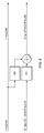
- FIG. 2B illustrates one embodiment of a signal generation system, including a digital circuit followed by a digital-to-analog conversion unit.
- FIG. 3 illustrates one embodiment of a method for correcting baseband I/Q gain and/or phase imbalance impairments in a signal digitizing system.
- FIG. 3B illustrates one embodiment of the signal digitization system, including a digitization unit followed by a digital circuit.
- FIG. 4 illustrates one embodiment of an inline measurement configuration where the inline gain imbalance is given by g m1 (f) and the phase skew is ⁇ m1 (f).
- FIG. 5 illustrates one embodiment of a crossed measurement configuration.
- FIG. 6 illustrates one embodiment of an effective crossed measurement configuration.
- FIG. 7 illustrates noise performance for a general calculation (with the assumption of no cross terms), according to one embodiment.
- FIG. 8 illustrates noise performance assuming zero receiver cross term, according to one embodiment.
- FIG. 9 illustrates noise performance assuming zero transmitter cross term, according to one embodiment.
- FIG. 10 illustrates noise performance with intentional gain imbalance at the transmitter equal to 0.95, according to one embodiment.
- FIG. 11 illustrates noise performance with intentional gain imbalance at the transmitter equal to 0.8, according to one embodiment.
- FIG. 12 illustrates noise performance with intentional gain imbalance at the transmitter equal to 0.5, according to one embodiment.
- FIG. 13 illustrates one embodiment of a general system model for derivation of impairment equations.
- FIG. 14 replicates equations 7.10 through 7.14 from the specification, for the reader's convenience.
- FIG. 15 illustrates one embodiment of a computer system 1500 that may be used to perform any of the method embodiments described herein.
- a memory medium is a non-transitory medium configured for the storage and retrieval of information.
- Examples of memory media include: various kinds of semiconductor-based memory such as RAM and ROM (including static RAM and dynamic RAM of various kinds, and PROM, EPROM, EEPROM and flash memory of various kinds); various kinds of magnetic media such as magnetic disk, tape, strip and film; various kinds of optical media such as CD-ROM, DVD-ROM and holographic media; various media based on the storage of electrical charge and/or any of a wide variety of other physical quantities; media fabricated using various lithographic techniques; etc.
- various kinds of semiconductor-based memory such as RAM and ROM (including static RAM and dynamic RAM of various kinds, and PROM, EPROM, EEPROM and flash memory of various kinds); various kinds of magnetic media such as magnetic disk, tape, strip and film; various kinds of optical media such as CD-ROM, DVD-ROM and holographic media; various media based on the storage of electrical charge and/or any of a wide variety of other physical quantities; media fabricated using various lithographic
- memory medium includes within its scope of meaning the possibility that a given memory medium might be a union of two or more memory media that reside at different locations, e.g., on different chips in a system or on different computers in a network.
- a memory medium is typically computer-readable, e.g., is capable of being read by a computer.
- Programmable Hardware Element includes various hardware devices comprising multiple programmable function blocks connected via a programmable interconnect. Examples include FPGAs (Field Programmable Gate Arrays), PLDs (Programmable Logic Devices), FPOAs (Field Programmable Object Arrays), and CPLDs (Complex PLDs).
- the programmable function blocks may range from fine grained (combinatorial logic or look up tables) to coarse grained (arithmetic logic units or processor cores).
- a programmable hardware element may also be referred to as “reconfigurable logic”.
- Computer System any of various types of computing or processing systems, including a personal computer system (PC), mainframe computer system, workstation, network appliance, Internet appliance, personal digital assistant (PDA), television system, grid computing system, or other device or combinations of devices.
- PC personal computer system
- mainframe computer system workstation
- network appliance Internet appliance
- PDA personal digital assistant
- television system grid computing system, or other device or combinations of devices.
- computer system can be broadly defined to encompass any device (or combination of devices) having at least one processor that executes instructions from a memory medium.
- Embodiments of the present invention may be realized in any of various forms.
- the present invention may be realized as a computer-implemented method, a computer-readable memory medium, or a computer system.
- the present invention may be realized using one or more custom-designed hardware devices such as ASICs.
- the present invention may be realized using one or more programmable hardware elements such as FPGAs.
- a computer-readable memory medium may be configured so that it stores program instructions and/or data, where the program instructions, if executed by a computer system, cause the computer system to perform a method, e.g., any of a method embodiments described herein, or, any combination of the method embodiments described herein, or, any subset of any of the method embodiments described herein, or, any combination of such subsets.
- a computer system may be configured to include a processor (or a set of processors) and a memory medium, where the memory medium stores program instructions, where the processor is configured to read and execute the program instructions from the memory medium, where the program instructions are executable to implement any of the various method embodiments described herein (or, any combination of the method embodiments described herein, or, any subset of any of the method embodiments described herein, or, any combination of such subsets).
- the computer system may be realized in any of various forms.
- the computer system may be a personal computer (in any of its various realizations), a workstation, a computer on a card, an application-specific computer in a box, a server computer, a client computer, a hand-held device, a tablet computer, a wearable computer, etc.
- a set of computers distributed across a network may be configured to partition the effort of executing a computational method (e.g., any of the method embodiments disclosed herein).
- a method 100 for determining gain and/or phase imbalance of a signal generation system and/or a signal digitizing system may include the operations shown in FIG. 1 . (The method 100 may also include any subset of the features, elements and embodiments described below in connection with FIGS. 4-15 .)
- the signal generation system may include one or more waveform generators.
- the signal digitizing system may include one or more waveform generators.
- the method includes (1) directing the signal generation system to generate a first vector calibration signal and to transmit a first vector output signal via the first output and the second output based on the first vector calibration signal, and (2) directing the signal digitizing system to capture a first set of vector samples from the first input and second input in response to the transmission of the first vector output signal.
- vector samples includes a corresponding sample of the first input and a corresponding sample of the second input.
- the method includes (3) directing the signal generation system to generate a second vector calibration signal and transmit a second vector output signal based on the second vector calibration signal, and (4) directing the signal digitizing system to capture a second set of vector samples from the first input and second input in response to the transmission of the second vector output signal.
- each of the vector samples includes a corresponding sample of the first input and a corresponding sample of the second input.
- the method includes computing a measurement of gain and/or phase imbalance of the signal generation system and/or a measurement of gain and/or phase imbalance of the signal digitizing system based on input data including the first set of vector samples and the second set of vector samples, e.g., as variously described below.
- FIG. 1B illustrates an initial connection configuration between the signal generation system 160 and signal digitizing system 165 , where the first output 162 A is connected to the first input 163 A via the first electrical conductor EC 1 , and the second output 162 B is connected to the second input 163 B via the second electrical conductor EC 2 .
- This initial connection configuration may be used to perform the acquisition operation 110 .
- FIG. 1C illustrates a second connection configuration between the signal generation system 160 and signal digitizing system 165 , wherein the first output 162 A is connected to the second input 163 B via the first electrical conductor EC 1 , and the second output 162 B is connected to the first input 163 A via the second electrical conductor EC 2 .
- This second connection configuration may be used perform the acquisition operation 115 , e.g., especially when the impairment(s) of the signal digitizing system are being determined.
- FIG. 1D illustrates a third connection configuration between the signal generation system 160 and signal digitizing system 165 , wherein the first output 162 A is connected to the second input 163 B via the second electrical conductor EC 2 , and the second output 162 B is connected to the first input 163 A via the first electrical conductor EC 1 .
- This third connection configuration may be used perform the acquisition operation 115 , e.g., especially when the impairment(s) of the signal generation system are being determined.
- the signal generation system includes a single dual-channel waveform generator.
- the signal generation system includes two single-channel waveform generators.
- the signal digitizing system includes a single dual-channel waveform digitizer.
- the signal digitizing system includes two single-channel waveform digitizers.
- the first vector calibration signal and the second vector calibration signal are identical, e.g., as variously described below. In other embodiments, the first vector calibration signal and the second vector calibration signal are different, e.g., as variously described below.
- the signal generation system is a waveform generator, where the first and second outputs are respectively I and Q outputs of the waveform generator.
- a waveform generator is a device that is configured to generate signals based on a specified sequence of samples. For example, a user-defined program may supply the sequence of samples to the waveform generator, and/or, may supply a set of parameters defining the sequence of samples.
- the waveform generator is a baseband waveform generator, wherein the I and Q outputs are baseband outputs.
- the waveform generator may also include circuitry to convert the I and Q baseband outputs into an RF output signal.
- Waveform generators are available from any of a wide variety of manufacturers and suppliers. For example, National Instruments Corp. produces waveform generators such as NI PXI-5421, NI PXIe-5442, NI PXIe-5450, NI PXIe-5451, NI PXIe-5645R.
- the signal digitizing system is a waveform digitizer, where the first and second inputs are respectively I and Q inputs of the waveform digitizer.
- a waveform digitizer is a device that is configured to convert a baseband IQ signal comprising I and Q component signals into a sequence of vector samples. The sequence of vector samples are stored in memory and made available to other devices for any desired analysis or processing.
- Waveform digitizers are available from any of a wide variety of manufacturers and suppliers. For example, National Instruments Corp. produces waveform digitizers such as NI PXI-5122, NI PXI-5124, NI PXIe-5162, NI PXIe-5185, NI PXIe-5645R.
- the gain and/or phase imbalance of the signal generation system includes a magnitude imbalance (i.e., gain imbalance) and a phase imbalance (i.e., phase skew) between I and Q channels of the waveform generator.
- the gain and/or phase imbalance of the signal digitizing system includes a magnitude imbalance (i.e., gain imbalance) and phase imbalance (i.e., phase skew) between I and Q channels of the waveform digitizer.
- a magnitude imbalance i.e., gain imbalance
- phase imbalance i.e., phase skew
- the method 100 may also include storing the measurement of gain and/or phase imbalance of the signal generation system and/or the measurement of gain and/or phase imbalance of the signal digitizing system in a memory.
- the method 100 may also include correcting the phase and/or gain imbalance of the signal generation system using the measurement of the phase and/or gain imbalance of the signal generation system.
- the action of correcting the phase and/or gain imbalance of the signal generation system includes programming a programmable hardware element (such as an FPGA) in the signal generation system to implement a correction filter, wherein coefficients of the filter are determined from the measurement of the gain and phase imbalance of the signal generation system.
- the programmable hardware element may be configured to operate on digital baseband signals (e.g., I and Q signals) prior to digital-to-analog conversion within the signal generation system.
- the method 100 may also include correcting the phase and/or gain imbalance of the signal digitizing system using the measurement of the gain and/or phase imbalance of the signal digitizing system.
- the action of correcting the phase and/or gain imbalance of the signal digitizing system includes programming a programmable hardware element (such as an FPGA) in the signal digitizing system to implement a correction filter, where coefficients of the correction filter are determined from the measurement of the gain and/or phase imbalance of the signal digitizing system.
- the programmable hardware element may be configured to operate on the digital baseband signals (e.g., I and Q signals) supplied by the analog-to-digital conversion circuitry of the signal digitizing system.
- the action of connecting the first output and the second output of the signal generation system respectively to the second input and the first input of the signal digitizing system includes: (a) connecting the first electrical conductor from the first output of the signal generation system to the second input of the signal digitizing system; and (b) connecting the second electrical conductor from the second output of the signal generation system to the first input of the signal digitizing system.
- a user or an automated system may disconnect the first and second electrical conductors from the first and second inputs (while maintaining their connections to the first and second outputs), and then reconnect to the first and second inputs with swapped correspondence of conductors to inputs.
- the action of connecting the first output and the second output of the signal generation system respectively to the second input and the first input of the signal digitizing system includes: (a*) connecting the first electrical conductor from the second output of the signal generation system to the first input of the signal digitizing system; and (b*) connecting the second electrical conductor from the first output of the signal generation system to the second input of the signal digitizing system.
- a user or an automated system may disconnect the first and second electronical conductors from the first and second outputs (while maintaining their connections to the first and second inputs), and then reconnect to the first and second outputs with swapped correspondence of conductors to outputs.
- the first electrical conductor and the second electrical conductor are electrical cables.
- the first electrical conductor and the second electrical conductor are traces on a circuit board or conductive paths in an integrated circuit.
- the signal generation system is a baseband I/Q waveform generator
- the waveform digitizing system is a baseband I/Q waveform digitizer
- the first vector calibration signal and/or the second vector calibration signal includes intentionally-introduced gain and phase impairments to facilitate more accurate estimation of the gain and/or phase imbalance of the signal generation system and/or the signal digitizing system.
- the first vector calibration signal and/or the second vector calibration signal includes a complex exponential signal that is swept or stepped through a desired range of frequencies.
- a computer system for determining gain and/or phase imbalance of a signal generation system and/or a signal digitizing system may be configured as follows. (The computer system may also include any subset of the features, elements and embodiments described above and described below in connection with FIGS. 4-15 .)
- the signal generation system includes a first output and a second output, and the signal digitizing system includes a first input and a second input.
- the computer system includes a processor and memory.
- the memory stores program instructions, where the program instructions, when executed by the processor, cause the processor to implement the following operations.
- the processor In response to a first signal indicating that a first connection configuration has been achieved between the first and second outputs of the signal generation system and the first and second inputs of the signal digitizing system, the processor (a) directs the signal generation system to generate a first vector calibration signal and transmit a first vector output signal via the first and second outputs based on the first vector calibration signal, and (b) directs the signal digitizing system to capture a first set of vector samples from the first input and second input in response to the transmission of the first vector output signal.
- the first connection configuration includes a connection of a first electrical conductor between the first output and the first input, and a connection of a second electrical conductor between the second output and the second.
- the processor In response to a second signal indicating that a second connection configuration has been achieved between the first and second outputs of the signal generation system and the first and second inputs of the signal digitizing system, the processor (c) directs the signal generation system to generate a second vector calibration signal and transmit a second vector output signal via the first and second outputs based on the second vector calibration signal, and (d) directs the signal digitizing system to capture a second set of vector samples from the first input and second input in response to the transmission of the second vector output signal.
- the second connection configuration includes the first and second electrical conductors being configured so that the first output is connected to the second input, and second output is connected to the first input.
- the processor may compute a measurement of gain and/or phase imbalance of the signal generation system and/or a measurement of gain and/or phase imbalance of the signal digitizing system based on input data including the first set of vector samples and the second set of vector samples, e.g., as variously described below. (See especially the mathematical discussions below.)
- the first vector calibration signal and the second vector calibration signal are identical. In other embodiments, the first vector calibration signal and the second vector calibration signal are different.
- the computer system may also include an automated system configured to connect and disconnect the first and second electrical conductors from the first and second outputs of the signal generation system and the first and second inputs of the signal digitizing system in order to achieve the first connection configuration or the second connection configuration upon command from the processor.
- the automated system may be employed to support measurements on a series of signal generation systems and/or a series of signal digitizing systems, e.g., in a factory calibration environment.
- a computer system for determining gain and/or phase imbalance of a signal generation system and/or a signal digitizing system may be configured as follows. (The computer system may also include any subset of the features, elements and embodiments described above and described below in connection with FIGS. 4-15 .)
- the signal generation system includes a first output and a second output, and the signal digitizing system includes a first input and a second input.
- the computer system includes a processor and memory.
- the memory stores program instructions, wherein the program instructions, when executed by the processor, cause the processor to perform the following operations.
- the processor In response to a first indication indicating that a first connection configuration has been achieved between the first and second outputs of the signal generation system and the first and second inputs of the signal digitizing system, the processor (a) directs the signal generation system to generate a first vector calibration signal and transmit a first vector output signal via the first and second outputs based on the first vector calibration signal, and (b) directs the signal digitizing system to capture a first set of vector samples in response to the transmission of the first vector output signal.
- the first connection configuration includes an electrical connection between the first output and the first input, and an electrical connection between the second output and the second input.
- the processor In response to a second indication indicating that a second connection configuration has been achieved between the first and second outputs of the signal generation system and the first and second inputs of the signal digitizing system, the processor (c) directs the signal generation system to generate a second vector calibration signal and transmit the second vector output signal via the first and second outputs based on the second vector calibration signal, and (d) directs the signal digitizing system to capture a second set of vector samples in response to the transmission of the second vector calibration signal, wherein the second connection configuration includes an electrical connection between the first output and the second input, and an electrical connection between the second output and the first input.
- the processor may compute a measurement of gain and/or phase imbalance of the signal generation system and/or a measurement of gain and/or phase imbalance of the signal digitizing system based on input data including the first set and the second set of vector samples.
- the first vector calibration signal and the second vector calibration signal are identical. In other embodiments, the first vector calibration signal and the second vector calibration signal are different.
- an electronic switching device is coupled to the first and second outputs of the signal generation system and the first and second inputs of the signal digitizing system.
- the electronic switching device is configured to establish the first connection configuration or the second connection configuration upon command from the processor.
- the signal generation system and the signal digitizing system are incorporated in a common enclosure with the electronic switching device.
- the electronic switching device includes one or more relays.
- a method 200 for correcting baseband gain and/or phase imbalance impairments in a signal generation system may include the operations shown in FIG. 2 . (The method 200 may also include any subset of the features, elements and embodiments described above.)
- the gain and phase imbalance impairments may be impairments between a first signal output path and a second signal output path of the signal generation system.
- the method may include programming a digital correction circuit in the signal generation system to implement a digital filter.
- the digital correction circuit is configured at a location upstream from digital-to-analog conversion in the signal generation system.
- the digital filter includes at least one inline filter and at least one cross filter. Each inline filter is applied to either the first signal output path or the second signal output path. (In other words, each inline filter is inline with either the first signal output path or the second signal output path.)
- Each cross filter crosses from the first signal output path to the second signal output path or vice versa.
- the parameters of said at least one inline filter and parameters of said at least one cross filter have been determined based on: (1) a first set of vector samples captured by a signal digitizing system in response to the signal generation system's transmission of a first vector calibration signal with a first connection configuration between two outputs of the signal generation system and two inputs of the signal digitizing system; and (2) a second set of vector samples captured by the signal digitizing system in response to the signal generation system's transmission of a second vector calibration signal with a crossed connection configuration between the two outputs of the signal generation system and the two inputs of the signal digitizing system.
- Methods for computing the parameters based on the first and second sets of vector samples are described variously above and below.
- the method 200 may also include invoking an operational mode of the signal generation system after having programmed the digital correction circuit.
- the signal generation system may generate corrected signals at its two outputs by virtue of the correcting action of the digital correction circuit.
- the corrected signals may be used, e.g., to test a receiver.
- the corrected signals may be transmitted to a receiver under test.
- the receiver may be evaluated or measured based on the signals it captures in response to the transmission of the corrected signals.
- the digital correction circuit is a programmable hardware element (PHE) or a dedicated digital circuit such as an ASIC. In other embodiments, the digital correction circuit is a processor configured to operate under the control of stored program instructions.
- PHE programmable hardware element
- ASIC application specific integrated circuit
- the signal generation system is a waveform generator, where the first signal output path is an I channel of the waveform generator, and the second signal output path is a Q channel of the waveform generator.
- the digital filter includes only one inline filter and only one cross filter, wherein the inline filter and cross filter are configured so that only one of the following conditions hold:
- the inline filter is applied to the second signal output path and the cross filter crosses from the second signal output path to the first signal output path;
- the inline filter is applied to the first signal output path and the cross filter crosses from the second signal output path to the second signal output path.
- the cross filter compensates for unmatched cross talk between the channels
- the inline filter compensates for the gain and/or phase imbalance between the first signal output path and the second signal output path.
- the cross filter is identically zero, and the inline filter compensates for the gain and/or phase imbalance between the first signal output path and the second signal output path.
- the digital filter includes only the at least one inline filter and no cross filters.
- FIG. 2B illustrates an embodiment 250 of the signal generation system, including a digital circuit 255 , a digital-to-analog conversion unit 257 .
- the digital circuit 255 implements the above-described impairment correction(s) when programmed by the above-described method 200 .
- the digital circuit 255 receives inphase digital signal I(n) and quadrature digital signal Q(n), and generates filtered inphase digital signal I F (n) and filtered quadrature digital signal Q F (n).
- the DAC unit 257 generates inphase analog signal I(t) and quadrature analog signal Q(t) based on the filtered signals I F (n) and Q F (n).
- a method 300 for correcting baseband I/Q gain and/or phase imbalance impairments in a signal digitizing system may include the operations shown in FIG. 3 .
- the computer system may also include any subset of the features, elements and embodiments described above and described below in connection with FIGS. 4-15 .
- the baseband I/Q gain and/or phase imbalance impairments may be impairments between a first signal input path and a second signal input path of the signal digitizing system.
- the method includes programming a digital correction circuit in the signal digitizing system to implement a digital filter.
- the digital correction circuit is configured at a location downstream from analog-to-digital conversion in the signal digitizing system.
- the digital filter includes at least one inline filter and at least one cross filter. Each inline filter is applied to either the first signal input path or the second signal input path. (In other words, each inline filter is inline with either the first signal input path or the second signal input path.)
- Each cross filter crosses from the first signal input path to the second signal input path or vice versa.
- the parameters of said at least one inline filter and parameters of said at least one cross filter have been determined based on: (1) a first set of vector samples captured by the signal digitizing system in response to a transmission of a first vector calibration signal by a signal generation system with a first connection configuration between two outputs of the signal generation system and two inputs of the signal digitizing system; and (2) a second set of vector samples captured by the signal digitizing system in response to the signal generation system's transmission of a second vector calibration signal with a crossed connection configuration between the two outputs of the signal generation system and the two inputs of the signal digitizing system.
- Methods for determining the parameters of the filters based on the first and second vector samples sets are variously described above and below. See especially the mathematical discussions below.
- the method 300 may also include invoking an operational mode of the signal digitizing system after having programmed the digital correction circuit.
- the signal digitizing system may generate corrected digital signals at the outputs of the digital correction circuit (by virtue of the correcting action of the digital correction circuit).
- the signal digitizing system may be used, e.g., to test a transmitter.
- the transmitter under test may transmit signals to the signal digitizing system.
- the corrected signals generated by the digital correction circuit in response to the transmission may be used to evaluate or measure the transmitter under test.
- the digital correction circuit is a programmable hardware element (PHE) or a dedicated digital circuit such as an ASIC. In other embodiments, the digital correction circuit is a processor configured to operate under the control of stored program instructions.
- PHE programmable hardware element
- ASIC application specific integrated circuit
- the signal digitizing system is a waveform digitizer, where the first signal input path is an I channel of the waveform digitizer, and the second signal input path is a Q channel of the waveform digitizer.
- the digital filter includes only one inline filter and only one cross filter, where the inline filter and cross filter are configured so that only one of the following conditions hold:
- the inline filter is applied to the second signal input path and the cross filter crosses from the second signal input path to the first signal input path;
- the inline filter is applied to the first signal input path and the cross filter crosses from the second signal input path to the first signal input path.
- the cross filter compensates for unmatched cross talk between the first and second input paths
- the inline filter compensates for the gain and/or phase impairments between the first signal input path and the second signal input path.
- the cross filter is identically zero, and the inline filter compensates for the gain and/or phase impairments between the first signal input path and the second signal input path.
- the digital filter includes only the at least one inline filter and no cross filters.
- FIG. 3B illustrates one embodiment 350 of a signal digitizing system, including a digitization unit 355 and a digital circuit 360 .
- the digitization unit 355 receives inphase analog signal I(t) and quadrature analog signal Q(t), and generates inphase digital signal I(n) and quadrature digital signal Q(n).
- the digital circuit 360 filters the digital signal I(n) and Q(n) to produce filtered signals I F (n) and Q F (n), e.g., as variously described above and below.
- This section describes how to measure RX and TX impairments for baseband IQ inputs and outputs.
- all that is required is information content at the desired frequency offset and no power content at the image frequency.
- a calibration tone supplied by a calibration synthesizer can used to determine the impairments.
- the transmitter will attempt to generate a pure tone, and an IF receiver can be used to measure the impairments. In both cases, it is important that the calibrating device have some way to distinguish its impairments from the DUTs.
- FIG. 4 shows the setup for the “inline” measurement where the inline gain imbalance is given by g m1 (f) and the phase skew is ⁇ m1 (f).
- FIG. 5 shows the setup for making a “crossed” measurement. This results when I TX is connected to Q RX and Q TX is connected to I RX .
- the inputs need to first be related to the relative impairments that will be measured at the output. By crossing the I and Q channels, the impairments seen at the input to the receiver will be flipped in frequency such that a complex exponential tone produced at the transmitter at frequency f, will appear at the receivers inputs at ⁇ f.
- the convention adopted throughout this document places all impairments on the Q channel where the I channel is assumed perfect. Equations 5.1 thru 5.7 give the step-by-step transformation back to the standard convention.
- FIG. 6 shows the crossed setup where the crossed gain imbalance is given by g m2 (f) and the crossed phase skew is ⁇ m2 (f). While the inputs are not crossed in FIG. 6 , the inputs are equal to the effective crossed inputs.
- Equation 5.8 comes from equation 7.8 of the section entitled “Impairment Derivation”. Equation 5.9 expresses the inline measurement using the setup in FIG. 4 , and equation 5.10 expresses the crossed measurement using the setup in FIG. 6 .
- equations 5.13 and 5.17 By multiplying equations 5.13 and 5.17 we can recover the receiver's impairments by using equation 5.17. If equations 5.13 and 5.17 are divided, the transmitter's impairments can be determined from equation 5.19. From 5.18 and 5.19 we can either calculate the gain and phase of each equation to find the separated RX and TX gain imbalance and phase skew, or the gain imbalances and phase skews can be calculated from the direct gain imbalance and phase skew measurements shown in equations 5.20 through 5.23.
- Z RX ⁇ ( f ) Z m ⁇ ⁇ 1 ⁇ ( f ) ⁇ Z m ⁇ 2 * ⁇ ( - f ) ( 5.18 )
- Z TX ⁇ ( f ) Z m ⁇ ⁇ 1 ⁇ ( f ) Z m ⁇ ⁇ 2 * ⁇ ( - f ) ( 5.19 )
- g TX ⁇ ( f ) Mag
- Z RX ⁇ ( f ) Z m ⁇ ⁇ 1 ⁇ ( f ) ⁇ Z m ⁇ 2 ⁇ ( f ) ( 5.24 )
- Z TX ⁇ ( f ) Z m ⁇ ⁇ 1 ⁇ ( f )
- Z m ⁇ ⁇ 2 ⁇ ( f ) 5.25
- g TX ⁇ ( f ) Mag ⁇ ( Z TX ⁇ ( f
- Equation 5.30 and 5.31 are the result of the section entitled “Impairment Derivation”.
- Equations 5.32 and 5.33 represent the looping back the transmitter into the receiver in the inline configuration shown in FIG. 4 .
- Equations 5.34 and 5.35 are the result of the measuring using loopback in the crossed configuration given in FIG. 6 .
- the filters When correcting for IQ impairments using the architecture described in the section entitled “Impairment Derivation”, the filters will not correct for cross talk unless zero cross talk exists from Q to I. Instead the filters will make the I to Q cross talk match the Q to I cross talk.
- FIG. 13 illustrates one embodiment of a general system model. (If Q′ is set equal to sin(2 ⁇ ft), then the model specializes to an impairment-correction model. If Q is set equal to sin(2 ⁇ ft), then the model specializes to a corruption model, i.e, a model of how impairments are introduced into the system.)
- g in ⁇ ( f ) Mag ( g out ⁇ ( f ) * e j ⁇ ⁇ ⁇ out ⁇ ( f ) - j ⁇ ⁇ U ⁇ ( f ) V ⁇ ( f ) ) ( 7.17 )
- ⁇ in ⁇ ( f ) Phase ( g out ⁇ ( f ) * e j ⁇ ⁇ ⁇ out ⁇ ( f ) - j ⁇ ⁇ U ⁇ ( f ) V ⁇ ( f ) ) ( 7.18 )
- a method for determining I/Q impairments of a waveform generator and/or a waveform digitizer comprising:
- I/Q impairments of the waveform generator include a magnitude imbalance (i.e., gain imbalance) and phase imbalance (i.e., phase skew) between I and Q channels of the waveform generator.
- I/Q impairments of the waveform digitizer include a magnitude imbalance (i.e., gain imbalance) and phase imbalance (i.e., phase skew) between I and Q channels of the waveform digitizer.
- said correcting the I/Q impairments of the waveform generator includes programming a programmable hardware element (such as an FPGA) in the waveform generator to implement a correction filter, wherein coefficients of the filter are determined from the measurement of the I/Q impairments of the waveform generator.
- a programmable hardware element such as an FPGA
- said correcting the I/Q impairments of the waveform digitizer includes programming a programmable hardware element (such as an FPGA) in the waveform digitizer to implement a correction filter, wherein coefficients of the filter are determined from the measurement of the I/Q impairments of the waveform digitizer.
- a programmable hardware element such as an FPGA
- connecting the I output and the Q output of the waveform generator respectively to the Q input and the I input of the waveform digitizer comprises: connecting the first electrical conductor from the I output of the waveform generator to the Q input of the waveform digitizer; and connecting the second electrical conductor from the Q output of the waveform generator to the I input of the waveform digitizer.
- the calibration signal includes intentionally introduced gain and phase impairments to facilitate more accurate estimation of the I/Q impairments of the waveform generator and/or the I/Q impairments of the waveform digitizer.
- the calibration signal includes a sinusoid that is swept or stepped through a desired range of frequencies.
- a computer system for calibrating a waveform generator and/or a waveform digitizer wherein the waveform generator includes an I output and Q output, wherein the waveform digitizer includes an I input and a Q input
- the computer system comprising: a processor; and memory that stores program instructions, wherein the program instructions, when executed by the processor, cause the processor to:
- the waveform generator in response to a first signal indicating that a first connection configuration has been achieved between the I and Q outputs of the waveform generator and the I and Q inputs of the waveform digitizer, direct the waveform generator to produce a calibration signal at its I and Q outputs, and direct the waveform digitizer to capture a first set of I/Q samples in response to the generation of the calibration signal, wherein the first connection configuration includes a connection of a first electrical conductor between the I output of the waveform generator and the I input of the waveform digitizer, and a connection of a second electrical conductor between the Q output of the waveform generator and the Q input of the waveform digitizer; in response to a second signal indicating that a second connection configuration has been achieved between the I and Q outputs of the waveform generator and the I and Q inputs of the waveform digitizer, direct the waveform generator to produce the calibration signal at its I output and Q output, and direct the waveform digitizer to capture a second set of I/Q samples in response to the generation of the calibration signal, where
- the computer system of paragraph 10 further comprising: an automated system configured to connect and disconnect the first and second electrical conductors from the I and Q outputs of the waveform generator and the I and Q inputs of the waveform generator in order to achieve the first connection configuration or the second connection configuration upon command from the processor.
- a computer system for calibrating a waveform generator and/or a waveform digitizer wherein the waveform generator includes an I output and Q output, wherein the waveform digitizer includes an I input and a Q input
- the computer system comprising: a processor; and memory that stores program instructions, wherein the program instructions, when executed by the processor, cause the processor to:
- the waveform generator in response to a first signal indicating that a first connection configuration has been achieved between the I and Q outputs of the waveform generator and the I and Q inputs of the waveform digitizer, direct the waveform generator to produce a calibration signal at its I and Q outputs, and direct the waveform digitizer to capture a first set of I/Q samples in response to the generation of the calibration signal, wherein the first connection configuration includes an electrical connection between the I output of the waveform generator and the I input of the waveform digitizer, and an electrical connection between the Q output of the waveform generator and the Q input of the waveform digitizer;
- the waveform generator in response to a second signal indicating that a second connection configuration has been achieved between the I and Q outputs of the waveform generator and the I and Q inputs of the waveform digitizer, direct the waveform generator to produce the calibration signal at its I output and Q output, and direct the waveform digitizer to capture a second set of I/Q samples in response to the generation of the calibration signal, wherein the second connection configuration includes an electrical connection between the I output of the waveform generator and the Q input of the waveform digitizer, and an electrical connection between the Q output of the waveform generator and the I input of the waveform digitizer;
- a non-transitory computer-readable memory medium for calibrating a waveform generator and/or a waveform digitizer wherein the waveform generator includes an I output and Q output, wherein the waveform digitizer includes an I input and a Q input, wherein the memory medium stores program instructions, wherein the program instructions, when executed by a computer system, cause the computer system to:
- the waveform generator in response to a first signal indicating that a first connection configuration has been achieved between the I and Q outputs of the waveform generator and the I and Q inputs of the waveform digitizer, direct the waveform generator to produce a calibration signal at its I and Q outputs, and direct the waveform digitizer to capture a first set of I/Q samples in response to the generation of the calibration signal, wherein the first connection configuration includes a connection of a first electrical conductor between the I output of the waveform generator and the I input of the waveform digitizer, and a connection of a second electrical conductor between the Q output of the waveform generator and the Q input of the waveform digitizer;
- the waveform generator in response to a second signal indicating that a second connection configuration has been achieved between the I and Q outputs of the waveform generator and the I and Q inputs of the waveform digitizer, direct the waveform generator to produce the calibration signal at its I output and Q output, and direct the waveform digitizer to capture a second set of I/Q samples in response to the generation of the calibration signal, wherein the second connection configuration includes the first and second electrical conductors being configured so that the I output of the waveform generator is connected to the Q input of the waveform digitizer, and Q output of the waveform generator is connected to the I input of the waveform digitizer;
- a digital correction circuit in the waveform generator to implement a digital filter, wherein the digital correction circuit is configured prior to digital-to-analog conversion in the waveform generator, wherein the digital filter includes at least one inline filter and at least one cross filter, wherein each inline filter is applied to either the I channel or the Q channel, wherein each cross filter crosses from the I channel to the Q channel or vice versa.
- the inline filter is applied to the I channel and the cross filter crosses from the Q channel to the I channel.
- a digital correction circuit in the waveform digitizer to implement a digital filter, wherein the digital correction circuit is configured after to analog-to-digital conversion in the waveform digitizer, wherein the digital filter includes at least one inline filter and at least one cross filter, wherein each inline filter is applied to either the I channel or the Q channel, wherein each cross filter crosses from the I channel to the Q channel or vice versa.
- the inline filter is applied to the I channel and the cross filter crosses from the Q channel to the I channel.
- a computer system comprising: a processor; and memory that stores program instructions, wherein the program instructions, when executed by the processor, cause the processor to perform the method recited in any one of the paragraphs 16-21.
- a non-transitory computer-readable memory medium that stores program instructions, wherein the program instructions, when executed by a computer system, cause the computer system to perform the method recited in any one of the paragraphs 16-21.
- FIG. 15 illustrates one embodiment of a computer system 1500 that may be used to perform any of the method embodiments described herein, or, any combination of the method embodiments described herein, or any subset of any of the method embodiments described herein, or, any combination of such subsets.
- Computer system 1500 may include a processing unit 1510 , a system memory 1512 , a set 1515 of one or more storage devices, a communication bus 1520 , a set 1525 of input devices, and a display system 1530 .
- System memory 1512 may include a set of semiconductor devices such as RAM devices (and perhaps also a set of ROM devices).
- Storage devices 1515 may include any of various storage devices such as one or more memory media and/or memory access devices.
- storage devices 1515 may include devices such as a CD/DVD-ROM drive, a hard disk, a magnetic disk drive, magnetic tape drives, etc.
- Processing unit 1510 is configured to read and execute program instructions, e.g., program instructions stored in system memory 1512 and/or on one or more of the storage devices 1515 .
- Processing unit 1510 may couple to system memory 1512 through communication bus 1520 (or through a system of interconnected busses, or through a network).
- the program instructions configure the computer system 1500 to implement a method, e.g., any of the method embodiments described herein, or, any combination of the method embodiments described herein, or, any subset of any of the method embodiments described herein, or any combination of such subsets.
- Processing unit 1510 may include one or more processors (e.g., microprocessors).
- Input devices 1525 may include devices such as a keyboard, a mouse, a touch-sensitive pad, a touch-sensitive screen, a drawing pad, a track ball, a light pen, a data glove, eye orientation and/or head orientation sensors, a microphone (or set of microphones), or any combination thereof
- the display system 1530 may include any of a wide variety of display devices representing any of a wide variety of display technologies.
- the display system may be a computer monitor, a head-mounted display, a projector system, a volumetric display, or a combination thereof.
- the display system may include a plurality of display devices.
- the display system may include a printer and/or a plotter.
- the computer system 1500 may include other devices, e.g., devices such as one or more graphics accelerators, one or more speakers, a sound card, a video camera and a video card, a data acquisition system.
- devices such as one or more graphics accelerators, one or more speakers, a sound card, a video camera and a video card, a data acquisition system.
- computer system 1500 may include one or more communication devices 1535 , e.g., a network interface card for interfacing with a computer network.
- the communication device 1535 may include a specialized interface for communication via any of a variety of established communication standards or protocols (e.g., USB, Firewire, PCI, PCI Express, PXI).
- the computer system may be configured with a software infrastructure including an operating system, and perhaps also, one or more graphics APIs (such as OpenGL®, Direct3D, Java 3DTM).
- the software infrastructure may include National Instruments LabVIEWTM software, and/or, LabVIEWTM FPGA.
- the computer system 00 may be configured to interface with transmitter 1540 (e.g., a waveform generator).
- the transmitter may be configured to generate an I output signal and a Q output signal, e.g., as variously described herein.
- the transmitter may operate under the control of software executing on processor 1510 and/or software executing on the transmitter itself
- the computer system 1500 may be configured to interface with a receiver 1550 (e.g., a waveform digitizer).
- the receiver may be configured to receive an I input signal and a Q input signal, e.g., as variously described herein.
- the receiver may operate under the control of software executing on processor 1510 and/or software executing on the receiver itself
- the transmitter and/or the receiver may include one or more programmable hardware elements and/or one or more microprocessors for performing digital processing on digital data (e.g., on digital baseband signals), e.g., as variously described herein.
Abstract
Description
ITX=>QRX and QTX=>IRX,
and obtaining a different combined measurement and then performing a numerical calculation. The rest of this section describes the theory behind this calculation where the final equations for separating these two measurements into impairments for the transmitter and impairments for the receiver is given at the end.
ITX=>IRX and QTX=>QRX.
if Z TX(f)=Z* TX(−f) then M(f)=1 (5.40)
Z TX(f)=√{square root over (N(f))} (5.41)
Z TX(−f)=√{square root over (N*(f))} (5.42)
The equations above are replicated in
g out(f)=Mag(jU(f)+V(f)g in(f)*e jφ
φout(f)=Phase(jU(f)+V(f)g in(f)*e jφ
Solve for the Input Impairments
Claims (26)
Priority Applications (1)
| Application Number | Priority Date | Filing Date | Title |
|---|---|---|---|
| US14/519,463 US9088331B2 (en) | 2013-02-22 | 2014-10-21 | IQ baseband matching calibration technique |
Applications Claiming Priority (3)
| Application Number | Priority Date | Filing Date | Title |
|---|---|---|---|
| US201361768326P | 2013-02-22 | 2013-02-22 | |
| US14/186,727 US8873610B2 (en) | 2013-02-22 | 2014-02-21 | IQ baseband matching calibration technique |
| US14/519,463 US9088331B2 (en) | 2013-02-22 | 2014-10-21 | IQ baseband matching calibration technique |
Related Parent Applications (1)
| Application Number | Title | Priority Date | Filing Date |
|---|---|---|---|
| US14/186,727 Continuation US8873610B2 (en) | 2013-02-22 | 2014-02-21 | IQ baseband matching calibration technique |
Publications (2)
| Publication Number | Publication Date |
|---|---|
| US20150036731A1 US20150036731A1 (en) | 2015-02-05 |
| US9088331B2 true US9088331B2 (en) | 2015-07-21 |
Family
ID=51388120
Family Applications (2)
| Application Number | Title | Priority Date | Filing Date |
|---|---|---|---|
| US14/186,727 Active US8873610B2 (en) | 2013-02-22 | 2014-02-21 | IQ baseband matching calibration technique |
| US14/519,463 Active US9088331B2 (en) | 2013-02-22 | 2014-10-21 | IQ baseband matching calibration technique |
Family Applications Before (1)
| Application Number | Title | Priority Date | Filing Date |
|---|---|---|---|
| US14/186,727 Active US8873610B2 (en) | 2013-02-22 | 2014-02-21 | IQ baseband matching calibration technique |
Country Status (1)
| Country | Link |
|---|---|
| US (2) | US8873610B2 (en) |
Families Citing this family (7)
| Publication number | Priority date | Publication date | Assignee | Title |
|---|---|---|---|---|
| US8873610B2 (en) * | 2013-02-22 | 2014-10-28 | National Instruments Corporation | IQ baseband matching calibration technique |
| US9326174B1 (en) | 2014-10-15 | 2016-04-26 | National Instruments Corporation | Spectral stitching method to increase instantaneous bandwidth in vector signal analyzers |
| US9609653B2 (en) | 2014-10-15 | 2017-03-28 | National Instruments Corporation | Spectral stitching method to increase instantaneous bandwidth in vector signal generators |
| US10057020B2 (en) * | 2015-11-19 | 2018-08-21 | Tektronix, Inc. | Joint estimation of coefficients for skew, gain imbalance and channel response for signal sources |
| EP3507954B1 (en) | 2016-09-03 | 2021-10-20 | National Instruments Corporation | Time sequenced spectral stitching |
| US11711104B2 (en) * | 2019-10-21 | 2023-07-25 | The Charles Machine Works, Inc. | Noise minimization to communicate with a beacon |
| US11734202B2 (en) * | 2020-09-17 | 2023-08-22 | Baker Hughes Oilfield Operations Llc | Sensor interface |
Citations (3)
| Publication number | Priority date | Publication date | Assignee | Title |
|---|---|---|---|---|
| US20100312515A1 (en) * | 2008-10-16 | 2010-12-09 | Advantest Corporation | Test apparatus, performance board and calibration board |
| US20110109321A1 (en) * | 2009-11-11 | 2011-05-12 | Advantest Corporation | Test apparatus and electrical device |
| US8873610B2 (en) * | 2013-02-22 | 2014-10-28 | National Instruments Corporation | IQ baseband matching calibration technique |
-
2014
- 2014-02-21 US US14/186,727 patent/US8873610B2/en active Active
- 2014-10-21 US US14/519,463 patent/US9088331B2/en active Active
Patent Citations (5)
| Publication number | Priority date | Publication date | Assignee | Title |
|---|---|---|---|---|
| US20100312515A1 (en) * | 2008-10-16 | 2010-12-09 | Advantest Corporation | Test apparatus, performance board and calibration board |
| US8280667B2 (en) | 2008-10-16 | 2012-10-02 | Advantest Corporation | Test apparatus, performance board and calibration board |
| US20110109321A1 (en) * | 2009-11-11 | 2011-05-12 | Advantest Corporation | Test apparatus and electrical device |
| US8274296B2 (en) | 2009-11-11 | 2012-09-25 | Advantest Corporation | Test apparatus and electronic device that tests a device under test |
| US8873610B2 (en) * | 2013-02-22 | 2014-10-28 | National Instruments Corporation | IQ baseband matching calibration technique |
Also Published As
| Publication number | Publication date |
|---|---|
| US20150036731A1 (en) | 2015-02-05 |
| US20140241410A1 (en) | 2014-08-28 |
| US8873610B2 (en) | 2014-10-28 |
Similar Documents
| Publication | Publication Date | Title |
|---|---|---|
| US9088331B2 (en) | IQ baseband matching calibration technique | |
| US8938025B2 (en) | Correction of I/Q impairments in transmitters and receivers | |
| US8798207B2 (en) | Synchronizing receivers in a signal acquisition system | |
| US9735899B2 (en) | Device and method for calibrating antenna array systems | |
| US8638893B2 (en) | Mechanisms for the correction of I/Q impairments | |
| US9281907B2 (en) | Quadrature error correction using polynomial models in tone calibration | |
| CN104168068A (en) | Method and system for common-mode-rejection-ratio (cmrr) characterization of an integrated coherent receiver | |
| CN104125182A (en) | Transceiver IQ calibration system and associated method | |
| US20080211515A1 (en) | Method and Apparatus for Measuring Scattering Coefficient of Device Under Test | |
| US7996169B2 (en) | Method and apparatus for compensating S-parameters of passive circuits | |
| US20140327429A1 (en) | Vector network power meter | |
| JP6360901B2 (en) | Time domain measurement method with calibration in frequency domain | |
| US20150358929A1 (en) | Calibration of high frequency signal measurement systems | |
| US20120223732A1 (en) | Transmission device and method of testing transmission characteristic of dut | |
| KR20130117841A (en) | Measurement error correction method and electronic component characteristic measurement device | |
| CN111781441A (en) | Eye pattern testing method based on CZT and vector network analyzer | |
| US8706434B1 (en) | Nonlinear systems measurement system and method | |
| Adamian et al. | A novel procedure for characterization of multiport high-speed balanced devices | |
| US10768221B2 (en) | Test equipment, method for operating a test equipment and computer program | |
| US10203396B2 (en) | Measurement error correction method and electric component property measurement device | |
| CN114531164B (en) | Transmitter, receiver, signal transceiver and corresponding methods | |
| CN102435867A (en) | Calibrating device for measuring accuracy of remote frequency-carrier phase noise | |
| Mahalingam et al. | Analysis and evaluation of register transfer logic software defined radio performance | |
| CN112583478A (en) | Nonlinear characteristic testing device and method of coherent optical receiver | |
| JP7069585B2 (en) | Residual DC component measurement method, measuring device and system |
Legal Events
| Date | Code | Title | Description |
|---|---|---|---|
| AS | Assignment |
Owner name: NATIONAL INSTRUMENTS CORPORATION, TEXAS Free format text: ASSIGNMENT OF ASSIGNORS INTEREST;ASSIGNOR:DARK, STEPHEN L.;REEL/FRAME:034021/0972 Effective date: 20141021 |
|
| STCF | Information on status: patent grant |
Free format text: PATENTED CASE |
|
| MAFP | Maintenance fee payment |
Free format text: PAYMENT OF MAINTENANCE FEE, 4TH YEAR, LARGE ENTITY (ORIGINAL EVENT CODE: M1551); ENTITY STATUS OF PATENT OWNER: LARGE ENTITY Year of fee payment: 4 |
|
| AS | Assignment |
Owner name: WELLS FARGO BANK, NATIONAL ASSOCIATION, NORTH CAROLINA Free format text: SECURITY INTEREST;ASSIGNORS:NATIONAL INSTRUMENTS CORPORATION;PHASE MATRIX, INC.;REEL/FRAME:052935/0001 Effective date: 20200612 |
|
| AS | Assignment |
Owner name: WELLS FARGO BANK, NATIONAL ASSOCIATION, NORTH CAROLINA Free format text: SECURITY INTEREST;ASSIGNOR:NATIONAL INSTRUMENTS CORPORATION;REEL/FRAME:057280/0028 Effective date: 20210618 |
|
| MAFP | Maintenance fee payment |
Free format text: PAYMENT OF MAINTENANCE FEE, 8TH YEAR, LARGE ENTITY (ORIGINAL EVENT CODE: M1552); ENTITY STATUS OF PATENT OWNER: LARGE ENTITY Year of fee payment: 8 |
|
| AS | Assignment |
Owner name: NATIONAL INSTRUMENTS CORPORATION, TEXAS Free format text: RELEASE OF SECURITY INTEREST IN PATENTS (REEL/FRAME 057280/0028);ASSIGNOR:WELLS FARGO BANK, NATIONAL ASSOCIATION, AS ADMINISTRATIVE AGENT;REEL/FRAME:065231/0466 Effective date: 20231011 Owner name: PHASE MATRIX, INC., CALIFORNIA Free format text: RELEASE OF SECURITY INTEREST IN PATENTS (REEL/FRAME 052935/0001);ASSIGNOR:WELLS FARGO BANK, NATIONAL ASSOCIATION, AS ADMINISTRATIVE AGENT;REEL/FRAME:065653/0463 Effective date: 20231011 Owner name: NATIONAL INSTRUMENTS CORPORATION, TEXAS Free format text: RELEASE OF SECURITY INTEREST IN PATENTS (REEL/FRAME 052935/0001);ASSIGNOR:WELLS FARGO BANK, NATIONAL ASSOCIATION, AS ADMINISTRATIVE AGENT;REEL/FRAME:065653/0463 Effective date: 20231011 |