EP3502714A1 - Rogowski coil - Google Patents
Rogowski coil Download PDFInfo
- Publication number
- EP3502714A1 EP3502714A1 EP18211166.6A EP18211166A EP3502714A1 EP 3502714 A1 EP3502714 A1 EP 3502714A1 EP 18211166 A EP18211166 A EP 18211166A EP 3502714 A1 EP3502714 A1 EP 3502714A1
- Authority
- EP
- European Patent Office
- Prior art keywords
- circuit board
- winding
- board surface
- tracks
- rogowski coil
- Prior art date
- Legal status (The legal status is an assumption and is not a legal conclusion. Google has not performed a legal analysis and makes no representation as to the accuracy of the status listed.)
- Withdrawn
Links
Images

Classifications
-
- G—PHYSICS
- G01—MEASURING; TESTING
- G01R—MEASURING ELECTRIC VARIABLES; MEASURING MAGNETIC VARIABLES
- G01R15/00—Details of measuring arrangements of the types provided for in groups G01R17/00 - G01R29/00, G01R33/00 - G01R33/26 or G01R35/00
- G01R15/14—Adaptations providing voltage or current isolation, e.g. for high-voltage or high-current networks
- G01R15/18—Adaptations providing voltage or current isolation, e.g. for high-voltage or high-current networks using inductive devices, e.g. transformers
- G01R15/181—Adaptations providing voltage or current isolation, e.g. for high-voltage or high-current networks using inductive devices, e.g. transformers using coils without a magnetic core, e.g. Rogowski coils
-
- H—ELECTRICITY
- H01—ELECTRIC ELEMENTS
- H01F—MAGNETS; INDUCTANCES; TRANSFORMERS; SELECTION OF MATERIALS FOR THEIR MAGNETIC PROPERTIES
- H01F17/00—Fixed inductances of the signal type
- H01F17/0006—Printed inductances
- H01F17/0013—Printed inductances with stacked layers
-
- H—ELECTRICITY
- H01—ELECTRIC ELEMENTS
- H01F—MAGNETS; INDUCTANCES; TRANSFORMERS; SELECTION OF MATERIALS FOR THEIR MAGNETIC PROPERTIES
- H01F27/00—Details of transformers or inductances, in general
- H01F27/28—Coils; Windings; Conductive connections
-
- H—ELECTRICITY
- H01—ELECTRIC ELEMENTS
- H01F—MAGNETS; INDUCTANCES; TRANSFORMERS; SELECTION OF MATERIALS FOR THEIR MAGNETIC PROPERTIES
- H01F5/00—Coils
-
- H—ELECTRICITY
- H01—ELECTRIC ELEMENTS
- H01F—MAGNETS; INDUCTANCES; TRANSFORMERS; SELECTION OF MATERIALS FOR THEIR MAGNETIC PROPERTIES
- H01F5/00—Coils
- H01F5/003—Printed circuit coils
-
- H—ELECTRICITY
- H05—ELECTRIC TECHNIQUES NOT OTHERWISE PROVIDED FOR
- H05K—PRINTED CIRCUITS; CASINGS OR CONSTRUCTIONAL DETAILS OF ELECTRIC APPARATUS; MANUFACTURE OF ASSEMBLAGES OF ELECTRICAL COMPONENTS
- H05K1/00—Printed circuits
- H05K1/16—Printed circuits incorporating printed electric components, e.g. printed resistors, capacitors or inductors
- H05K1/165—Printed circuits incorporating printed electric components, e.g. printed resistors, capacitors or inductors incorporating printed inductors
-
- H—ELECTRICITY
- H01—ELECTRIC ELEMENTS
- H01F—MAGNETS; INDUCTANCES; TRANSFORMERS; SELECTION OF MATERIALS FOR THEIR MAGNETIC PROPERTIES
- H01F17/00—Fixed inductances of the signal type
- H01F17/0006—Printed inductances
- H01F17/0013—Printed inductances with stacked layers
- H01F2017/002—Details of via holes for interconnecting the layers
Definitions
- the invention relates to a Rogowski coil comprising:
- Such a Rogowski coil is for example known from GB 2342783 or US 20040178875 .
- GB 2342783 discloses a Rogowski coil arranged on a three layer printed circuit board. Tracks on the outer two layers are electrically connected by vias to form a winding around a central passage opening through which a current conducting conductor extends. The tracks are arranged alternately on the two outer layers, such that a plurality of turns is provided forming the winding. These turns make the winding susceptible for the magnetic field generated by the current in the conductor.
- the winding As the winding is arranged concentric around the conductor, the winding itself is also a turn being susceptible for a disturbing magnetic field perpendicular to the layer of the printed circuit board.
- GB 2342783 discloses to provide a counter turn enveloped by the winding on the inner layer of the printed circuit board.
- US 2004 0178875 describes a Rowgowski coil arranged on a five layer printed circuit board.
- the two most outer layers are used to provide a first winding.
- the two layers between the center layer and the outer layers is used to provide a second winding in the same direction as the first winding to increase the sensitivity of the Rogowski coil.
- Two counter turns are provided on the center layer to reduce any disturbing effects in the first and second windings.
- a Rogowski coil according to the preamble, which is characterized in that the second, return winding is formed by a plurality of tracks arranged alternately on the inner top circuit board surface and the inner bottom circuit board surface, wherein the plurality of tracks are electrically connected by vias extending from the inner top circuit board surface to the inner bottom circuit board surface; and wherein the first and second winding have opposite direction of rotation around the respective axis.
- the second, return winding increases the sensitivity of the Rogowski coil because the direction of rotation is opposite to the first winding.
- the second, return winding also provides a reduction of disturbances due to magneticfields perpendicular to the printed circuit boards. This is because the second, return winding also forms a turn around the central passage opening, similar to the first winding forms a turn around the central passage opening, but the second, return winding has an opposite direction (as it is the return winding) relative to the first winding.
- the arrangement of the first winding and the second, return winding on only four circuit board surfaces reduces the costs, for example compared to US 2004 0178875 , which requires five circuit board surfaces to have an equal sensitivity for the current measurement in the conductor extending through the central passage opening, while having a similar insensitivity for disturbing magnetic fields perpendicular to the printed circuit board.
- the advantage of the second, return winding to be enveloped by the first winding is that both windings are subjected to the same part of the magnetic field of any external sources. This further increases the accuracy of the Rogowski coil.
- the average line of the first winding coincides with the average line of the second winding when viewed in a direction perpendicular to the circuit board surfaces, which average line is defined as the line through the centers of gravity of each turn of a winding viewed in said direction perpendicular to the circuit board surfaces.
- the average line of a winding as defined above forms the effective turn, which is susceptible for disturbing magnetic fields perpendicular to the printed circuit board.
- the plurality of tracks of the first and second winding are straight. Using straight tracks allows for a simple design of the circuit board surfaces and allows for relative easy calculation of the centers of gravity of each turn, such that the windings can be designed such that the average lines coincide.
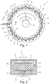
- FIG. 1 shows a Rogowski coil 1 according to the invention.
- the coil 1 has a printed circuit board 2 with a central passage opening 3 through which a conductor C extends.
- the Rogowski coil 1 has a first winding composed out of tracks 4, 5 and vias 6 and a second, return winding composed out of tracks 7, 8 and vias 9.
- the first winding 4, 5, 6 and the second, return winding 7, 8, 9 are arranged in series at the coupling 10, where the first winding is electrically connected to the second winding.
- the conductor C generates an magnetic field F, which causes a current I in the first winding 4, 5, 6 and the second, return winding 7, 8, 9. (see figure 2 ).
- the first and second winding have opposite direction of rotation around the respective axis and because the second winding 7, 8, 9 returns back towards the start 11 of the first winding 4, 5, 6, the current I in the first and second windings support each other, such that the sensitivity of the Rogowski coil 1 is increased.
- FIG. 3 shows a detail of the Rogowski coil 1 of figure 1 .
- the first winding 4, 5, 6 is depicted.
- a turn 12 of a first winding 4, 5, 6 is embodied by a track 4, a via 6, a track 5 and a second via 6.
- a winding Viewed in the direction perpendicular to the surface of the printed circuit board 2, a winding has a center of gravity 13.
- the average line 14 of a winding is formed by the curve extending through all centers of gravity 13.
- Figure 4 shows a schematic cross-section along the average line 14.
- a disturbing magnetic field F d falls perpendicular to the surface of the printed circuit board 2
- a current I 1 will be generated in the first winding 4, 5, 6, while an opposite current I 2 will be generated in the second, return winding 7, 8, 9.
- the currents I 1 and I 2 generated by the disturbing magnetic field F d , will cancel each other out, such that the Rogowski coil 1 will only measure the current in the conductor C.
Landscapes
- Engineering & Computer Science (AREA)
- Power Engineering (AREA)
- Physics & Mathematics (AREA)
- General Physics & Mathematics (AREA)
- Microelectronics & Electronic Packaging (AREA)
- Transformers For Measuring Instruments (AREA)
- Measuring Instrument Details And Bridges, And Automatic Balancing Devices (AREA)
- Coils Or Transformers For Communication (AREA)
Abstract
Description
- The invention relates to a Rogowski coil comprising:
- a multilayer printed circuit board having a plurality of layers forming at least an outer top circuit board surface, an outer bottom circuit board surface, an inner top circuit board surface and an inner bottom circuit board surface;
- a first winding formed by a plurality of tracks arranged alternately on the outer top circuit board surface and the outer bottom circuit board surface, wherein the plurality of tracks are electrically connected by vias extending from the outer top circuit board surface to the outer bottom circuit board surface;
- a second, return winding enveloped by the first winding;
- Such a Rogowski coil is for example known from
GB 2342783 US 20040178875 . -
GB 2342783 - As the winding is arranged concentric around the conductor, the winding itself is also a turn being susceptible for a disturbing magnetic field perpendicular to the layer of the printed circuit board.
- In order to reduce this disturbing effect,
GB 2342783 -
US 2004 0178875 describes a Rowgowski coil arranged on a five layer printed circuit board. The two most outer layers are used to provide a first winding. The two layers between the center layer and the outer layers is used to provide a second winding in the same direction as the first winding to increase the sensitivity of the Rogowski coil. Two counter turns are provided on the center layer to reduce any disturbing effects in the first and second windings. - It is an object of the invention to provide an alternative for the Rogowski coil constructions known in the prior art.
- This object is achieved with a Rogowski coil according to the preamble, which is characterized in that the second, return winding is formed by a plurality of tracks arranged alternately on the inner top circuit board surface and the inner bottom circuit board surface, wherein the plurality of tracks are electrically connected by vias extending from the inner top circuit board surface to the inner bottom circuit board surface; and
wherein the first and second winding have opposite direction of rotation around the respective axis. - With the Rogowski coil according to the invention, the second, return winding increases the sensitivity of the Rogowski coil because the direction of rotation is opposite to the first winding.
- Furthermore, the second, return winding also provides a reduction of disturbances due to magneticfields perpendicular to the printed circuit boards. This is because the second, return winding also forms a turn around the central passage opening, similar to the first winding forms a turn around the central passage opening, but the second, return winding has an opposite direction (as it is the return winding) relative to the first winding.
- The arrangement of the first winding and the second, return winding on only four circuit board surfaces reduces the costs, for example compared to
US 2004 0178875 , which requires five circuit board surfaces to have an equal sensitivity for the current measurement in the conductor extending through the central passage opening, while having a similar insensitivity for disturbing magnetic fields perpendicular to the printed circuit board. - The advantage of the second, return winding to be enveloped by the first winding, is that both windings are subjected to the same part of the magnetic field of any external sources. This further increases the accuracy of the Rogowski coil.
- In a preferred embodiment of the Rogowski coil according to the invention the average line of the first winding coincides with the average line of the second winding when viewed in a direction perpendicular to the circuit board surfaces, which average line is defined as the line through the centers of gravity of each turn of a winding viewed in said direction perpendicular to the circuit board surfaces.
- The average line of a winding as defined above forms the effective turn, which is susceptible for disturbing magnetic fields perpendicular to the printed circuit board. By having the average line of the first winding to coincide with the average line of the second, return winding, it is ensured that the disturbing field is fully cancelled.
- In a further embodiment of the Rogowski coil according to the invention the plurality of tracks of the first and second winding are straight. Using straight tracks allows for a simple design of the circuit board surfaces and allows for relative easy calculation of the centers of gravity of each turn, such that the windings can be designed such that the average lines coincide.
- It will be apparent for the person skilled in the art, that the number of windings can be increased by increasing the number of layers of the PCB. As a result, a Rogowski coil according to the invention could be created having two first windings with two second, return windings all arranged in series and enveloped by each other.
- These and other features of the invention will be elucidated in conjunction with the accompanying drawings.
-
Figure 1 shows a schematic top view of a Rogowski coil according to the invention. -
Figure 2 shows a cross-section of the Rogowski coil offigure 1 . -
Figure 3 shows a detail of the coil offigure 1 . -
Figure 4 shows a schematic cross-section along the average line shown infigure 3 . -
Figure 1 shows a Rogowskicoil 1 according to the invention. Thecoil 1 has a printedcircuit board 2 with a central passage opening 3 through which a conductor C extends. - The Rogowski
coil 1 has a first winding composed out oftracks vias 6 and a second, return winding composed out oftracks vias 9. The first winding 4, 5, 6 and the second, return winding 7, 8, 9 are arranged in series at thecoupling 10, where the first winding is electrically connected to the second winding. - The conductor C generates an magnetic field F, which causes a current I in the first winding 4, 5, 6 and the second, return winding 7, 8, 9. (see
figure 2 ). As the first and second winding have opposite direction of rotation around the respective axis and because the second winding 7, 8, 9 returns back towards thestart 11 of the first winding 4, 5, 6, the current I in the first and second windings support each other, such that the sensitivity of the Rogowskicoil 1 is increased. -
Figure 3 shows a detail of the Rogowskicoil 1 offigure 1 . Thefirst winding turn 12 of afirst winding track 4, avia 6, atrack 5 and a second via 6. Viewed in the direction perpendicular to the surface of the printedcircuit board 2, a winding has a center ofgravity 13. As a result, theaverage line 14 of a winding is formed by the curve extending through all centers ofgravity 13. -
Figure 4 shows a schematic cross-section along theaverage line 14. When a disturbing magnetic field Fd falls perpendicular to the surface of the printedcircuit board 2, a current I1 will be generated in thefirst winding coil 1 will only measure the current in the conductor C.
Claims (3)
- Rogowski coil (1) comprising:- a multilayer printed circuit board (2) having a plurality of layers forming at least an outer top circuit board surface, an outer bottom circuit board surface, an inner top circuit board surface and an inner bottom circuit board surface;- a first winding (4, 5, 6) formed by a plurality of tracks (4, 5) arranged alternately on the outer top circuit board surface and the outer bottom circuit board surface, wherein the plurality of tracks (4, 5) are electrically connected by vias (6) extending from the outer top circuit board surface to the outer bottom circuit board surface;- a second, return winding (7, 8, 9) enveloped by the first winding (4, 5, 6);wherein the multilayer printed circuit board (2) comprises a central passage opening (3) for passage of a current conducting conductor (C), wherein the axes of the first and second winding (4, 5, 6; 7, 8, 9) are arranged concentric around the central passage opening (3), and wherein the first and second winding (4, 5, 6; 7, 8, 9) are electrically arranged in series;
characterized in that- the second, return winding (7, 8, 9) is formed by a plurality of tracks (7, 8) arranged alternately on the inner top circuit board surface and the inner bottom circuit board surface, wherein the plurality of tracks (7, 8) are electrically connected by vias (9) extending from the inner top circuit board surface to the inner bottom circuit board surface; andwherein the first and second winding (4, 5, 6; 7, 8, 9) have opposite direction of rotation around the respective axis. - Rogowski coil (1) according to claim 1, wherein the average line (14) of the first winding (4, 5, 6) coincides with the average line of the second winding (7, 8, 9) when viewed in a direction perpendicular to the circuit board surfaces, which average line (14) is defined as the line through the centers of gravity (13) of each turn of a winding (4, 5, 6) viewed in said direction perpendicular to the circuit board surfaces.
- Rogowski coil (1) according to claim 1 or 2, wherein the plurality of tracks (4, 5; 7, 8) of the first and second winding (4, 5, 6; 7, 8, 9) are straight.
Applications Claiming Priority (1)
| Application Number | Priority Date | Filing Date | Title |
|---|---|---|---|
| GB1721357.0A GB2569563A (en) | 2017-12-20 | 2017-12-20 | Rogowski coil |
Publications (1)
| Publication Number | Publication Date |
|---|---|
| EP3502714A1 true EP3502714A1 (en) | 2019-06-26 |
Family
ID=61008744
Family Applications (1)
| Application Number | Title | Priority Date | Filing Date |
|---|---|---|---|
| EP18211166.6A Withdrawn EP3502714A1 (en) | 2017-12-20 | 2018-12-07 | Rogowski coil |
Country Status (5)
| Country | Link |
|---|---|
| US (1) | US10877073B2 (en) |
| EP (1) | EP3502714A1 (en) |
| JP (1) | JP2019114787A (en) |
| GB (1) | GB2569563A (en) |
| ZA (1) | ZA201808371B (en) |
Cited By (1)
| Publication number | Priority date | Publication date | Assignee | Title |
|---|---|---|---|---|
| WO2021136710A1 (en) | 2019-12-31 | 2021-07-08 | Eaton Intelligent Power Limited | Sensor part for installation in medium-voltage cable compartments and a device for measuring a voltage in medium-voltage circuits comprising such sensor part |
Families Citing this family (1)
| Publication number | Priority date | Publication date | Assignee | Title |
|---|---|---|---|---|
| JP2024538073A (en) * | 2022-03-15 | 2024-10-18 | アナログ・ディヴァイシス・インターナショナル・アンリミテッド・カンパニー | Current Sensors |
Citations (3)
| Publication number | Priority date | Publication date | Assignee | Title |
|---|---|---|---|---|
| JP2005175156A (en) * | 2003-12-10 | 2005-06-30 | Mitsubishi Electric Corp | Air-core coil and air-core coil manufacturing method |
| US20080079418A1 (en) * | 2006-09-29 | 2008-04-03 | Gm Global Technology Operations, Inc. | High-precision rogowski current transformer |
| WO2013114137A1 (en) * | 2012-02-03 | 2013-08-08 | Power Electronic Measurements Limited | Temperature compensated current measurement |
Family Cites Families (6)
| Publication number | Priority date | Publication date | Assignee | Title |
|---|---|---|---|---|
| GB9821164D0 (en) | 1998-09-30 | 1998-11-25 | Ward David | Measuring device |
| US6313623B1 (en) * | 2000-02-03 | 2001-11-06 | Mcgraw-Edison Company | High precision rogowski coil |
| JP2004119926A (en) * | 2002-09-30 | 2004-04-15 | Toshiba Corp | Current transformer and current transformer system |
| JP4674557B2 (en) * | 2006-02-23 | 2011-04-20 | パナソニック電工株式会社 | AC current detection coil |
| US7545138B2 (en) * | 2006-07-06 | 2009-06-09 | Schweitzer Engineering Laboratories, Inc. | Precision, temperature-compensated, shielded current measurement device |
| JP6455812B2 (en) * | 2014-02-24 | 2019-01-23 | パナソニックIpマネジメント株式会社 | Current measuring device |
-
2017
- 2017-12-20 GB GB1721357.0A patent/GB2569563A/en not_active Withdrawn
-
2018
- 2018-12-07 EP EP18211166.6A patent/EP3502714A1/en not_active Withdrawn
- 2018-12-11 ZA ZA2018/08371A patent/ZA201808371B/en unknown
- 2018-12-18 US US16/223,140 patent/US10877073B2/en active Active
- 2018-12-19 JP JP2018237586A patent/JP2019114787A/en active Pending
Patent Citations (3)
| Publication number | Priority date | Publication date | Assignee | Title |
|---|---|---|---|---|
| JP2005175156A (en) * | 2003-12-10 | 2005-06-30 | Mitsubishi Electric Corp | Air-core coil and air-core coil manufacturing method |
| US20080079418A1 (en) * | 2006-09-29 | 2008-04-03 | Gm Global Technology Operations, Inc. | High-precision rogowski current transformer |
| WO2013114137A1 (en) * | 2012-02-03 | 2013-08-08 | Power Electronic Measurements Limited | Temperature compensated current measurement |
Cited By (2)
| Publication number | Priority date | Publication date | Assignee | Title |
|---|---|---|---|---|
| WO2021136710A1 (en) | 2019-12-31 | 2021-07-08 | Eaton Intelligent Power Limited | Sensor part for installation in medium-voltage cable compartments and a device for measuring a voltage in medium-voltage circuits comprising such sensor part |
| GB2590987A (en) | 2019-12-31 | 2021-07-14 | Eaton Intelligent Power Ltd | Sensor part for installation in medium-voltage cable compartments and a device for measuring a voltage in medium-voltage circuits comprising such sensor part |
Also Published As
| Publication number | Publication date |
|---|---|
| ZA201808371B (en) | 2025-12-17 |
| US20190187185A1 (en) | 2019-06-20 |
| GB2569563A (en) | 2019-06-26 |
| JP2019114787A (en) | 2019-07-11 |
| US10877073B2 (en) | 2020-12-29 |
| GB201721357D0 (en) | 2018-01-31 |
Similar Documents
| Publication | Publication Date | Title |
|---|---|---|
| RU2719794C2 (en) | Current sensor and device for measuring electric current | |
| JP4842562B2 (en) | Current transformer including a combination of partial circuits with a Rogowski type winding forming a complete circuit | |
| US7579824B2 (en) | High-precision Rogowski current transformer | |
| US8686822B2 (en) | Surface mounted pulse transformer | |
| US9869565B2 (en) | Rotation detection device and method of manufacturing rotation detection device | |
| US20120146620A1 (en) | Current sensor | |
| IES20010370A2 (en) | Current measurement device | |
| EP3502714A1 (en) | Rogowski coil | |
| US11290079B2 (en) | Device for filtering at least one signal | |
| JPWO2016132666A1 (en) | Common mode noise filter | |
| JP5756910B2 (en) | Printed circuit boards, current sensors and distribution boards | |
| US20230162905A1 (en) | Planar transformer including noise cancellation for auxiliary winding | |
| US11443887B2 (en) | Planar transformer having integrated ring core | |
| US11549969B2 (en) | Low-noise, large dynamic-range sensor for measuring current | |
| EP3120159B1 (en) | Flexible circuit rogowski coil | |
| US9111678B2 (en) | Planar core-type uniform external field equalizer and fabrication | |
| US20250062763A1 (en) | Sensor element and inductive sensor | |
| JP5557308B2 (en) | Electric leakage detection device and method of arranging coils of electric leakage detection device | |
| CN103383401B (en) | The external disturbance compensation method of U-shaped PCB coil binding clip | |
| JP6855601B2 (en) | Current detector | |
| GB2526579A (en) | Sensor for measuring current in a conductor | |
| CN113130181B (en) | Transformer and electromagnetic device using same | |
| JP2013207150A (en) | Common mode filter | |
| WO2012049565A1 (en) | Current measuring device for electric lines | |
| CN119213695A (en) | Proximity switch and method for detecting a trigger |
Legal Events
| Date | Code | Title | Description |
|---|---|---|---|
| PUAI | Public reference made under article 153(3) epc to a published international application that has entered the european phase |
Free format text: ORIGINAL CODE: 0009012 |
|
| STAA | Information on the status of an ep patent application or granted ep patent |
Free format text: STATUS: THE APPLICATION HAS BEEN PUBLISHED |
|
| AK | Designated contracting states |
Kind code of ref document: A1 Designated state(s): AL AT BE BG CH CY CZ DE DK EE ES FI FR GB GR HR HU IE IS IT LI LT LU LV MC MK MT NL NO PL PT RO RS SE SI SK SM TR |
|
| AX | Request for extension of the european patent |
Extension state: BA ME |
|
| STAA | Information on the status of an ep patent application or granted ep patent |
Free format text: STATUS: REQUEST FOR EXAMINATION WAS MADE |
|
| 17P | Request for examination filed |
Effective date: 20191210 |
|
| RBV | Designated contracting states (corrected) |
Designated state(s): AL AT BE BG CH CY CZ DE DK EE ES FI FR GB GR HR HU IE IS IT LI LT LU LV MC MK MT NL NO PL PT RO RS SE SI SK SM TR |
|
| STAA | Information on the status of an ep patent application or granted ep patent |
Free format text: STATUS: EXAMINATION IS IN PROGRESS |
|
| 17Q | First examination report despatched |
Effective date: 20200120 |
|
| RAP1 | Party data changed (applicant data changed or rights of an application transferred) |
Owner name: EATON INTELLIGENT POWER LIMITED |
|
| STAA | Information on the status of an ep patent application or granted ep patent |
Free format text: STATUS: THE APPLICATION IS DEEMED TO BE WITHDRAWN |
|
| 18D | Application deemed to be withdrawn |
Effective date: 20200731 |