EP3501040B1 - Dual deep trenches for high voltage isolation - Google Patents
Dual deep trenches for high voltage isolation Download PDFInfo
- Publication number
- EP3501040B1 EP3501040B1 EP17842059.2A EP17842059A EP3501040B1 EP 3501040 B1 EP3501040 B1 EP 3501040B1 EP 17842059 A EP17842059 A EP 17842059A EP 3501040 B1 EP3501040 B1 EP 3501040B1
- Authority
- EP
- European Patent Office
- Prior art keywords
- trench
- buried layer
- substrate
- layer
- conductor
- Prior art date
- Legal status (The legal status is an assumption and is not a legal conclusion. Google has not performed a legal analysis and makes no representation as to the accuracy of the status listed.)
- Active
Links
- 238000002955 isolation Methods 0.000 title description 8
- 230000009977 dual effect Effects 0.000 title description 2
- 239000000758 substrate Substances 0.000 claims description 67
- 238000000034 method Methods 0.000 claims description 57
- 230000005684 electric field Effects 0.000 claims description 45
- 239000004020 conductor Substances 0.000 claims description 30
- 230000015556 catabolic process Effects 0.000 claims description 23
- 238000005530 etching Methods 0.000 claims description 4
- 239000004065 semiconductor Substances 0.000 description 96
- 230000008569 process Effects 0.000 description 45
- 239000000463 material Substances 0.000 description 27
- 239000002019 doping agent Substances 0.000 description 16
- VYPSYNLAJGMNEJ-UHFFFAOYSA-N Silicium dioxide Chemical compound O=[Si]=O VYPSYNLAJGMNEJ-UHFFFAOYSA-N 0.000 description 14
- 239000008186 active pharmaceutical agent Substances 0.000 description 8
- 150000004767 nitrides Chemical class 0.000 description 8
- 238000004519 manufacturing process Methods 0.000 description 7
- 235000012239 silicon dioxide Nutrition 0.000 description 7
- 239000000377 silicon dioxide Substances 0.000 description 7
- 238000009826 distribution Methods 0.000 description 5
- 229910021420 polycrystalline silicon Inorganic materials 0.000 description 5
- BOTDANWDWHJENH-UHFFFAOYSA-N Tetraethyl orthosilicate Chemical compound CCO[Si](OCC)(OCC)OCC BOTDANWDWHJENH-UHFFFAOYSA-N 0.000 description 4
- 229910052785 arsenic Inorganic materials 0.000 description 4
- RQNWIZPPADIBDY-UHFFFAOYSA-N arsenic atom Chemical compound [As] RQNWIZPPADIBDY-UHFFFAOYSA-N 0.000 description 4
- XUIMIQQOPSSXEZ-UHFFFAOYSA-N Silicon Chemical compound [Si] XUIMIQQOPSSXEZ-UHFFFAOYSA-N 0.000 description 3
- 230000008901 benefit Effects 0.000 description 3
- 230000008878 coupling Effects 0.000 description 3
- 238000010168 coupling process Methods 0.000 description 3
- 238000005859 coupling reaction Methods 0.000 description 3
- 238000000623 plasma-assisted chemical vapour deposition Methods 0.000 description 3
- 229920005591 polysilicon Polymers 0.000 description 3
- 229910052710 silicon Inorganic materials 0.000 description 3
- 239000010703 silicon Substances 0.000 description 3
- QGZKDVFQNNGYKY-UHFFFAOYSA-N Ammonia Chemical compound N QGZKDVFQNNGYKY-UHFFFAOYSA-N 0.000 description 2
- KRHYYFGTRYWZRS-UHFFFAOYSA-N Fluorane Chemical compound F KRHYYFGTRYWZRS-UHFFFAOYSA-N 0.000 description 2
- 230000015572 biosynthetic process Effects 0.000 description 2
- 238000004518 low pressure chemical vapour deposition Methods 0.000 description 2
- 238000000926 separation method Methods 0.000 description 2
- OAICVXFJPJFONN-UHFFFAOYSA-N Phosphorus Chemical compound [P] OAICVXFJPJFONN-UHFFFAOYSA-N 0.000 description 1
- 229910052581 Si3N4 Inorganic materials 0.000 description 1
- BLRPTPMANUNPDV-UHFFFAOYSA-N Silane Chemical compound [SiH4] BLRPTPMANUNPDV-UHFFFAOYSA-N 0.000 description 1
- 230000004913 activation Effects 0.000 description 1
- 229910021529 ammonia Inorganic materials 0.000 description 1
- 238000000137 annealing Methods 0.000 description 1
- 239000007864 aqueous solution Substances 0.000 description 1
- 238000005229 chemical vapour deposition Methods 0.000 description 1
- 230000000593 degrading effect Effects 0.000 description 1
- 238000005137 deposition process Methods 0.000 description 1
- 239000003989 dielectric material Substances 0.000 description 1
- 238000009792 diffusion process Methods 0.000 description 1
- 229910052731 fluorine Inorganic materials 0.000 description 1
- 239000011737 fluorine Substances 0.000 description 1
- 239000007789 gas Substances 0.000 description 1
- 230000003116 impacting effect Effects 0.000 description 1
- 239000007943 implant Substances 0.000 description 1
- 238000011065 in-situ storage Methods 0.000 description 1
- 239000012212 insulator Substances 0.000 description 1
- 230000014759 maintenance of location Effects 0.000 description 1
- 230000003647 oxidation Effects 0.000 description 1
- 238000007254 oxidation reaction Methods 0.000 description 1
- 229910052698 phosphorus Inorganic materials 0.000 description 1
- 239000011574 phosphorus Substances 0.000 description 1
- 229920002120 photoresistant polymer Polymers 0.000 description 1
- 229910000077 silane Inorganic materials 0.000 description 1
- HQVNEWCFYHHQES-UHFFFAOYSA-N silicon nitride Chemical compound N12[Si]34N5[Si]62N3[Si]51N64 HQVNEWCFYHHQES-UHFFFAOYSA-N 0.000 description 1
- 239000000243 solution Substances 0.000 description 1
- 238000001228 spectrum Methods 0.000 description 1
- 239000000126 substance Substances 0.000 description 1
- 230000008719 thickening Effects 0.000 description 1
Images


Classifications
-
- H—ELECTRICITY
- H01—ELECTRIC ELEMENTS
- H01L—SEMICONDUCTOR DEVICES NOT COVERED BY CLASS H10
- H01L27/00—Devices consisting of a plurality of semiconductor or other solid-state components formed in or on a common substrate
- H01L27/02—Devices consisting of a plurality of semiconductor or other solid-state components formed in or on a common substrate including semiconductor components specially adapted for rectifying, oscillating, amplifying or switching and having at least one potential-jump barrier or surface barrier; including integrated passive circuit elements with at least one potential-jump barrier or surface barrier
- H01L27/04—Devices consisting of a plurality of semiconductor or other solid-state components formed in or on a common substrate including semiconductor components specially adapted for rectifying, oscillating, amplifying or switching and having at least one potential-jump barrier or surface barrier; including integrated passive circuit elements with at least one potential-jump barrier or surface barrier the substrate being a semiconductor body
- H01L27/08—Devices consisting of a plurality of semiconductor or other solid-state components formed in or on a common substrate including semiconductor components specially adapted for rectifying, oscillating, amplifying or switching and having at least one potential-jump barrier or surface barrier; including integrated passive circuit elements with at least one potential-jump barrier or surface barrier the substrate being a semiconductor body including only semiconductor components of a single kind
- H01L27/085—Devices consisting of a plurality of semiconductor or other solid-state components formed in or on a common substrate including semiconductor components specially adapted for rectifying, oscillating, amplifying or switching and having at least one potential-jump barrier or surface barrier; including integrated passive circuit elements with at least one potential-jump barrier or surface barrier the substrate being a semiconductor body including only semiconductor components of a single kind including field-effect components only
- H01L27/088—Devices consisting of a plurality of semiconductor or other solid-state components formed in or on a common substrate including semiconductor components specially adapted for rectifying, oscillating, amplifying or switching and having at least one potential-jump barrier or surface barrier; including integrated passive circuit elements with at least one potential-jump barrier or surface barrier the substrate being a semiconductor body including only semiconductor components of a single kind including field-effect components only the components being field-effect transistors with insulated gate
- H01L27/092—Devices consisting of a plurality of semiconductor or other solid-state components formed in or on a common substrate including semiconductor components specially adapted for rectifying, oscillating, amplifying or switching and having at least one potential-jump barrier or surface barrier; including integrated passive circuit elements with at least one potential-jump barrier or surface barrier the substrate being a semiconductor body including only semiconductor components of a single kind including field-effect components only the components being field-effect transistors with insulated gate complementary MIS field-effect transistors
- H01L27/0922—Combination of complementary transistors having a different structure, e.g. stacked CMOS, high-voltage and low-voltage CMOS
-
- H—ELECTRICITY
- H01—ELECTRIC ELEMENTS
- H01L—SEMICONDUCTOR DEVICES NOT COVERED BY CLASS H10
- H01L21/00—Processes or apparatus adapted for the manufacture or treatment of semiconductor or solid state devices or of parts thereof
- H01L21/70—Manufacture or treatment of devices consisting of a plurality of solid state components formed in or on a common substrate or of parts thereof; Manufacture of integrated circuit devices or of parts thereof
- H01L21/71—Manufacture of specific parts of devices defined in group H01L21/70
- H01L21/76—Making of isolation regions between components
- H01L21/762—Dielectric regions, e.g. EPIC dielectric isolation, LOCOS; Trench refilling techniques, SOI technology, use of channel stoppers
- H01L21/76224—Dielectric regions, e.g. EPIC dielectric isolation, LOCOS; Trench refilling techniques, SOI technology, use of channel stoppers using trench refilling with dielectric materials
- H01L21/76229—Concurrent filling of a plurality of trenches having a different trench shape or dimension, e.g. rectangular and V-shaped trenches, wide and narrow trenches, shallow and deep trenches
-
- H—ELECTRICITY
- H01—ELECTRIC ELEMENTS
- H01L—SEMICONDUCTOR DEVICES NOT COVERED BY CLASS H10
- H01L21/00—Processes or apparatus adapted for the manufacture or treatment of semiconductor or solid state devices or of parts thereof
- H01L21/70—Manufacture or treatment of devices consisting of a plurality of solid state components formed in or on a common substrate or of parts thereof; Manufacture of integrated circuit devices or of parts thereof
- H01L21/71—Manufacture of specific parts of devices defined in group H01L21/70
- H01L21/76—Making of isolation regions between components
- H01L21/763—Polycrystalline semiconductor regions
-
- H—ELECTRICITY
- H01—ELECTRIC ELEMENTS
- H01L—SEMICONDUCTOR DEVICES NOT COVERED BY CLASS H10
- H01L21/00—Processes or apparatus adapted for the manufacture or treatment of semiconductor or solid state devices or of parts thereof
- H01L21/70—Manufacture or treatment of devices consisting of a plurality of solid state components formed in or on a common substrate or of parts thereof; Manufacture of integrated circuit devices or of parts thereof
- H01L21/71—Manufacture of specific parts of devices defined in group H01L21/70
- H01L21/76—Making of isolation regions between components
- H01L21/765—Making of isolation regions between components by field effect
-
- H—ELECTRICITY
- H01—ELECTRIC ELEMENTS
- H01L—SEMICONDUCTOR DEVICES NOT COVERED BY CLASS H10
- H01L21/00—Processes or apparatus adapted for the manufacture or treatment of semiconductor or solid state devices or of parts thereof
- H01L21/70—Manufacture or treatment of devices consisting of a plurality of solid state components formed in or on a common substrate or of parts thereof; Manufacture of integrated circuit devices or of parts thereof
- H01L21/77—Manufacture or treatment of devices consisting of a plurality of solid state components or integrated circuits formed in, or on, a common substrate
- H01L21/78—Manufacture or treatment of devices consisting of a plurality of solid state components or integrated circuits formed in, or on, a common substrate with subsequent division of the substrate into plural individual devices
- H01L21/82—Manufacture or treatment of devices consisting of a plurality of solid state components or integrated circuits formed in, or on, a common substrate with subsequent division of the substrate into plural individual devices to produce devices, e.g. integrated circuits, each consisting of a plurality of components
- H01L21/822—Manufacture or treatment of devices consisting of a plurality of solid state components or integrated circuits formed in, or on, a common substrate with subsequent division of the substrate into plural individual devices to produce devices, e.g. integrated circuits, each consisting of a plurality of components the substrate being a semiconductor, using silicon technology
- H01L21/8232—Field-effect technology
- H01L21/8234—MIS technology, i.e. integration processes of field effect transistors of the conductor-insulator-semiconductor type
- H01L21/8238—Complementary field-effect transistors, e.g. CMOS
- H01L21/823871—Complementary field-effect transistors, e.g. CMOS interconnection or wiring or contact manufacturing related aspects
-
- H—ELECTRICITY
- H01—ELECTRIC ELEMENTS
- H01L—SEMICONDUCTOR DEVICES NOT COVERED BY CLASS H10
- H01L21/00—Processes or apparatus adapted for the manufacture or treatment of semiconductor or solid state devices or of parts thereof
- H01L21/70—Manufacture or treatment of devices consisting of a plurality of solid state components formed in or on a common substrate or of parts thereof; Manufacture of integrated circuit devices or of parts thereof
- H01L21/77—Manufacture or treatment of devices consisting of a plurality of solid state components or integrated circuits formed in, or on, a common substrate
- H01L21/78—Manufacture or treatment of devices consisting of a plurality of solid state components or integrated circuits formed in, or on, a common substrate with subsequent division of the substrate into plural individual devices
- H01L21/82—Manufacture or treatment of devices consisting of a plurality of solid state components or integrated circuits formed in, or on, a common substrate with subsequent division of the substrate into plural individual devices to produce devices, e.g. integrated circuits, each consisting of a plurality of components
- H01L21/822—Manufacture or treatment of devices consisting of a plurality of solid state components or integrated circuits formed in, or on, a common substrate with subsequent division of the substrate into plural individual devices to produce devices, e.g. integrated circuits, each consisting of a plurality of components the substrate being a semiconductor, using silicon technology
- H01L21/8232—Field-effect technology
- H01L21/8234—MIS technology, i.e. integration processes of field effect transistors of the conductor-insulator-semiconductor type
- H01L21/8238—Complementary field-effect transistors, e.g. CMOS
- H01L21/823878—Complementary field-effect transistors, e.g. CMOS isolation region manufacturing related aspects, e.g. to avoid interaction of isolation region with adjacent structure
-
- H—ELECTRICITY
- H01—ELECTRIC ELEMENTS
- H01L—SEMICONDUCTOR DEVICES NOT COVERED BY CLASS H10
- H01L21/00—Processes or apparatus adapted for the manufacture or treatment of semiconductor or solid state devices or of parts thereof
- H01L21/70—Manufacture or treatment of devices consisting of a plurality of solid state components formed in or on a common substrate or of parts thereof; Manufacture of integrated circuit devices or of parts thereof
- H01L21/77—Manufacture or treatment of devices consisting of a plurality of solid state components or integrated circuits formed in, or on, a common substrate
- H01L21/78—Manufacture or treatment of devices consisting of a plurality of solid state components or integrated circuits formed in, or on, a common substrate with subsequent division of the substrate into plural individual devices
- H01L21/82—Manufacture or treatment of devices consisting of a plurality of solid state components or integrated circuits formed in, or on, a common substrate with subsequent division of the substrate into plural individual devices to produce devices, e.g. integrated circuits, each consisting of a plurality of components
- H01L21/822—Manufacture or treatment of devices consisting of a plurality of solid state components or integrated circuits formed in, or on, a common substrate with subsequent division of the substrate into plural individual devices to produce devices, e.g. integrated circuits, each consisting of a plurality of components the substrate being a semiconductor, using silicon technology
- H01L21/8232—Field-effect technology
- H01L21/8234—MIS technology, i.e. integration processes of field effect transistors of the conductor-insulator-semiconductor type
- H01L21/8238—Complementary field-effect transistors, e.g. CMOS
- H01L21/823892—Complementary field-effect transistors, e.g. CMOS with a particular manufacturing method of the wells or tubs, e.g. twin tubs, high energy well implants, buried implanted layers for lateral isolation [BILLI]
-
- H—ELECTRICITY
- H01—ELECTRIC ELEMENTS
- H01L—SEMICONDUCTOR DEVICES NOT COVERED BY CLASS H10
- H01L29/00—Semiconductor devices adapted for rectifying, amplifying, oscillating or switching, or capacitors or resistors with at least one potential-jump barrier or surface barrier, e.g. PN junction depletion layer or carrier concentration layer; Details of semiconductor bodies or of electrodes thereof ; Multistep manufacturing processes therefor
- H01L29/02—Semiconductor bodies ; Multistep manufacturing processes therefor
- H01L29/06—Semiconductor bodies ; Multistep manufacturing processes therefor characterised by their shape; characterised by the shapes, relative sizes, or dispositions of the semiconductor regions ; characterised by the concentration or distribution of impurities within semiconductor regions
- H01L29/0603—Semiconductor bodies ; Multistep manufacturing processes therefor characterised by their shape; characterised by the shapes, relative sizes, or dispositions of the semiconductor regions ; characterised by the concentration or distribution of impurities within semiconductor regions characterised by particular constructional design considerations, e.g. for preventing surface leakage, for controlling electric field concentration or for internal isolations regions
- H01L29/0607—Semiconductor bodies ; Multistep manufacturing processes therefor characterised by their shape; characterised by the shapes, relative sizes, or dispositions of the semiconductor regions ; characterised by the concentration or distribution of impurities within semiconductor regions characterised by particular constructional design considerations, e.g. for preventing surface leakage, for controlling electric field concentration or for internal isolations regions for preventing surface leakage or controlling electric field concentration
- H01L29/0611—Semiconductor bodies ; Multistep manufacturing processes therefor characterised by their shape; characterised by the shapes, relative sizes, or dispositions of the semiconductor regions ; characterised by the concentration or distribution of impurities within semiconductor regions characterised by particular constructional design considerations, e.g. for preventing surface leakage, for controlling electric field concentration or for internal isolations regions for preventing surface leakage or controlling electric field concentration for increasing or controlling the breakdown voltage of reverse biased devices
- H01L29/0615—Semiconductor bodies ; Multistep manufacturing processes therefor characterised by their shape; characterised by the shapes, relative sizes, or dispositions of the semiconductor regions ; characterised by the concentration or distribution of impurities within semiconductor regions characterised by particular constructional design considerations, e.g. for preventing surface leakage, for controlling electric field concentration or for internal isolations regions for preventing surface leakage or controlling electric field concentration for increasing or controlling the breakdown voltage of reverse biased devices by the doping profile or the shape or the arrangement of the PN junction, or with supplementary regions, e.g. junction termination extension [JTE]
-
- H—ELECTRICITY
- H01—ELECTRIC ELEMENTS
- H01L—SEMICONDUCTOR DEVICES NOT COVERED BY CLASS H10
- H01L29/00—Semiconductor devices adapted for rectifying, amplifying, oscillating or switching, or capacitors or resistors with at least one potential-jump barrier or surface barrier, e.g. PN junction depletion layer or carrier concentration layer; Details of semiconductor bodies or of electrodes thereof ; Multistep manufacturing processes therefor
- H01L29/02—Semiconductor bodies ; Multistep manufacturing processes therefor
- H01L29/06—Semiconductor bodies ; Multistep manufacturing processes therefor characterised by their shape; characterised by the shapes, relative sizes, or dispositions of the semiconductor regions ; characterised by the concentration or distribution of impurities within semiconductor regions
- H01L29/0603—Semiconductor bodies ; Multistep manufacturing processes therefor characterised by their shape; characterised by the shapes, relative sizes, or dispositions of the semiconductor regions ; characterised by the concentration or distribution of impurities within semiconductor regions characterised by particular constructional design considerations, e.g. for preventing surface leakage, for controlling electric field concentration or for internal isolations regions
- H01L29/0642—Isolation within the component, i.e. internal isolation
- H01L29/0649—Dielectric regions, e.g. SiO2 regions, air gaps
Definitions
- Integrated circuits with high voltage capabilities have wide industrial applications, including power management systems for use in automobiles. These integrated circuits include high voltage transistors that operate at a high voltage range (e.g., 80v to 120v) and low voltage transistors that operate at a much lower voltage range (e.g., 1v to 5v).
- a buried layer e.g., an N-type buried layer
- a bulk substrate e.g., a P-type substrate
- the buried layer is usually biased at a high voltage corresponding to the operating range of the high voltage transistors, whereas the bulk substrate is usually biased at a ground supply voltage.
- the difference between the high bias voltage and the ground supply voltage may exceed a breakdown voltage threshold of a PN junction between the buried layer and the bulk substrate, thereby causing leakages and impacting the performance and reliability of the integrated circuit.
- US2013/328123 relates to a semiconductor including a first trench structure and a second trench structure.
- EP 1 710 834 discloses a double trench for isolation of semiconductor devices.
- the semiconductor device may be a standalone discrete component or incorporated as a part of an integrated circuit.
- the semiconductor device adopts an isolation scheme to protect low voltage transistors from high voltage operations.
- the described isolation scheme allows the high voltage transistors to operate at a high voltage range while reducing the voltage stress between a buried layer and a bulk substrate of the semiconductor device.
- the described isolation scheme provides a low-cost and high-performance solution to alleviate junction breakdowns of the semiconductor device.
- an integrated circuit includes a substrate, a buried layer, a transistor well region, a first trench, and a second trench.
- the substrate has a top surface and a bottom surface.
- the buried layer is positioned within the substrate, and the transistor well region is positioned above the buried layer.
- the first trench extends from the top surface to penetrate the buried layer, and the first trench has a first trench depth.
- the second trench extends from the top surface to penetrate the buried layer.
- the second trench is interposed between the first trench and the transistor well region.
- the second trench has a second trench depth that is less than the first trench depth.
- the substrate has a first conductivity type
- the buried layer has a second conductivity type opposite of the first conductivity type.
- the first trench includes a first conductor that is insulated from the buried layer and making an ohmic contact with the substrate around a bottom portion of the first trench, whereas the second trench includes a second conductor insulated from the buried layer and the substrate.
- the method includes forming a buried layer within a substrate.
- the method also includes forming a transistor well region above the buried layer.
- the method further includes forming a first trench extending from a top surface of the substrate to penetrate the buried layer, and forming a second trench extending from the top surface of the substrate to penetrate the buried layer. More specifically, the second trench is interposed between the first trench and the transistor well region, and the second trench has a trench depth less than that of the first trench.
- the method further includes the step of forming a first conductor within the first trench, the first conductor insulated from the buried layer and making an ohmic contact with the substrate around a bottom portion of the first trench; and the step of forming a second conductor within the second trench, the second conductor insulated from the buried layer and the substrate.
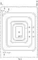
- FIG. 1A shows a top view of a semiconductor device 100
- FIG. 1B shows a cross-sectional view of the semiconductor device 100 to illustrate its vertical structure.
- the semiconductor device 100 includes a substrate 102, which can be subdivided into a lower semiconductor layer 104 and an upper semiconductor layer 108.
- the lower semiconductor layer 104 forms a bottom surface 102b of the substrate 102
- the upper semiconductor layer 108 forms a top surface 102a of the substrate 102.
- the lower semiconductor layer 104 may be a part of a bulk silicon substrate (e.g., 102), an epitaxial layer on a bulk silicon wafer, or a silicon-on-insulator (SOI) wafer.
- SOI silicon-on-insulator
- the upper semiconductor layer 108 may be an epitaxial layer formed above the lower semiconductor layer 102, or as an extension of a bulk silicon substrate (e.g., 102).
- the lower and upper semiconductor layer 104 and 108 usually have the same conductivity type (e.g., P-type).
- the semiconductor device 100 includes a buried layer 106 positioned within the substrate 102.
- the buried layer 106 may be developed by doping the lower semiconductor layer 104.
- the buried layer 106 may be formed by growing an epitaxial layer with in situ doping on top of the lower semiconductor layer 104.
- the buried layer 106 is interposed between the lower and upper semiconductor layers 104 and 108, and the buried layer 106 has the opposite conductivity type from these two layers 104 and 108. Accordingly, the buried layer 106 forms a first PN junction 105 with the lower semiconductor layer 104 and a second PN junction 107 with the upper semiconductor layer 108.
- the buried layer 106 may have an average doping density of at least 1 ⁇ 10 18 cm-3 and commonly has an opposite conductivity type from the lower semiconductor layer 104.
- a top boundary 112 of the buried layer 106 is at least 2 microns below the top surface 102a of the substrate 102, and may extend 5 microns to 10 microns below the top surface 102a of the substrate 102.
- the buried layer 106 may extend laterally across the semiconductor device 100 as depicted in FIG. 1 , or alternatively, the buried layer may be developed or formed within a finite lateral region that is coplanar with the substrate 102.
- the semiconductor device 100 includes a transistor well region 101 that is positioned within the upper semiconductor layer 108 and above the buried layer 106.
- the transistor well region 101 includes transistors for forming one or more active circuits.
- the transistor well region 101 includes a low voltage circuit (e.g., a circuit that operates with less than 10v)
- the transistor well region 101 is isolated and protected from a high voltage circuit (e.g., a circuit that operates with more than 50v) formed outside of the transistor well region 101.
- the transistor well region 101 includes a high voltage circuit
- the transistor well region 101 is isolated to protect a low voltage circuit formed outside of the transistor well region 101.
- the semiconductor device 100 includes one or more deep trench structures 114 arranged to laterally surround the transistor well region 101 and intersect the buried layer 106. More specifically, the deep trench structure 114 extends from the top surface 102a to penetrate through the buried layer 106, thereby reaching the lower semiconductor layer 104.
- the deep trench structure 114 may have a trench width 120 of less than 6 um. In one example implementation, the trench width 120 may range from 1 micron to 4 microns.
- the deep trench structure 114 includes dielectric liners 116 disposed along the interior sidewalls. The dielectric liners 116 may include thermal silicon dioxide.
- the deep trench structure 114 defines a bottom opening for accessing the lower semiconductor layer 104 of the substrate 102.
- the access point is doped with a dopant of the same conductivity type as the lower semiconductor layer 104 to form a doped region 117. In one implementation, the doped region 117 may have a higher doping concentration than the lower semiconductor layer 104.
- the deep trench structure 114 includes trench fill material 118 disposed onto the dielectric liners 116.
- the trench fill material 118 is conductive, and it is insulated from the upper semiconductor layer 108 and the buried layer 106.
- the trench fill material 118 includes polycrystalline silicon, which is commonly referred to as polysilicon.
- the trench fill material (i.e., trench conductor) 118 establishes an ohmic contact with the lower semiconductor layer 104 of the substrate 102 via the bottom opening and the doped region 117. Through this ohmic contact, the trench conductor 118 can be used for biasing the lower semiconductor layer 104 of the substrate 102.
- the trench conductor 118 may be structured to receive a ground supply voltage V GND to bias the lower semiconductor layer 104 of the substrate 102.
- the buried layer 106 When being biased at a voltage V BIAS corresponding to the operation voltage range of the high voltage circuit, the buried layer 106 can be used as an isolation structure as well.
- the bias voltage V BIAS of the buried layer 106 may range from 100v to 170v.
- the semiconductor device 100 includes vertical doped structures (a.k.a. sinkers) 122 that extend from the top surface 102a to reach the buried layer 106.
- the sinkers 122 are doped with dopants of the same conductivity type as the buried layer 106 so as to provide electrical connections to the buried layer 106.
- the sinkers 122 are doped with N-type materials where the buried layer 106 is N-doped as well.
- the sinkers 122 may be formed alongside the deep trench structure 114.
- the sinkers 122 extend laterally from the deep trench structure 114 to have a thickness 124, and the sinkers 122 coextend with the deep trench structure 114 to provide a conductive path between the top surface 102a and the buried layer 106.
- the thickness 124 of the sinkers is less than 2.5 microns, which may advantageously reduce the size of the semiconductor device 100 when compared to semiconductor devices without self-alignment sinkers.
- the trench structure 114 and the sinkers 122 form a contiguous ring that circumscribes the transistor well region 101.
- the trench structure 114 and the sinkers 122 may be arranged as disconnected and discrete segments to approximate the contiguous ring for isolating the transistor well region 101.
- the upper semiconductor layer 108 may incur a relatively high voltage where the transistor well region 101 includes one or more high voltage circuits.
- the upper semiconductor layer 108 may incur a voltage ranges from 80v to 100v.
- the buried layer 106 is biased with a voltage V BIAS that is higher than the voltage incurred by the upper semiconductor layer 108.
- the bias voltage V BIAS may range from 100v to 170v.
- the bias voltage V BIAS may range from 140v to 170v.
- the bias voltage V BIAS may range from 145v to 155v.
- the potential difference between the buried layer 106 and the lower semiconductor layer 104 can become significantly large. And when this potential difference becomes larger than the breakdown voltage (e.g., less than 80v) of the first PN junction 105, the semiconductor device 100 may experience a substantial amount of current leakage.
- This potential difference can be illustrated by an electric field density spread across a high electric field line V 1 and a low electric field line V 2 .
- the high electric field line V 1 represents a potential distribution closer to the bias voltage V BIAS
- the low electric field line V 2 represents a potential distribution closer to the ground supply voltage V GND .
- the likelihood of having a breakdown at the first PN junction 105 is directly proportional to the potential difference between V 1 and V 2 , and inversely proportional to a distance between V 1 and V 2 .
- thickening the dielectric liner 116 may help increase the low electric field line V 2 as the ground potential carried by the trench conductor 118 exerts less capacitive coupling to the adjacent P-region of the lower semiconductor layer 104.
- the potential difference between V 1 and V 2 can be reduced to lower the likelihood of having a breakdown along the first PN junction 105.
- This approach may be less effective where V 1 is substantially higher than V 2 (e.g., V 1 - V 2 ⁇ 100v) and the maximum thickness of the dielectric liner 116 is limited by one or more process parameters.
- increasing the thickness of the buried layer 106 may help reduce the electric field density between V 1 and V 2 to avoid electric field crowding along the first PN junction 105.
- the potential gradient at the first PN junction 105 can be reduced to lower the likelihood of having a breakdown along the first PN junction 105.
- This approach may be costly where V 1 is substantially higher than V 2 (e.g., V 1 - V 2 ⁇ 100v) because a thickened buried layer 106 usually requires more material and time to develop, and it can be more difficult to etch in forming the deep trench structure 114.
- the buried layer 106 may include an upper buried layer 106a with a first doping concentration and a lower buried layer 106b with a second doping concentration that is lower than the first doping concentration.
- the upper buried layer 106a may have a doping concentration that is greater than 5 ⁇ 10 18 cm -3
- the lower buried layer 106b may have a doping concentration ranging from 1 ⁇ 10 16 cm -3 to 1 ⁇ 10 17 cm -3 .
- example embodiments introduce a dual-trench configuration that alleviates electric field crowding around the first PN junction 105 between the buried layer 106 and the lower semiconductor layer 104 of the substrate 102.
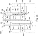
- FIG. 1C shows a top view of a semiconductor device 100A with a dual-trench configuration
- FIG. ID shows a cross-sectional view of the semiconductor device 100A according to an aspect of example embodiments.
- the semiconductor device 100A is similar to the semiconductor device 100 to the extent that these two devices include components identified with the same numeric labels.
- the semiconductor device 100A differs from the semiconductor device 100 in that the semiconductor device 100A includes a second deep trench structure 174.
- the second deep trench structure 174 is arranged to laterally surround the transistor well region 101 and intersect the buried layer 106. More specifically, the second deep trench structure 174 extends from the top surface 102a to penetrate the buried layer 106. In one example implementation, the second deep trench structure 174 may penetrate through the buried layer 106 to reach the lower semiconductor layer 104 of the substrate 102. In another example implementation, the second deep trench structure 174 may partially penetrate the buried layer 106 and terminate within the buried layer 106. The second deep trench structure 174 is interposed between the first deep trench structure 114 and the transistor well region 101. As shown in FIG. 1C , the second deep trench structure 174 circumscribes the transistor well region 101, while being circumscribed by the first deep trench structure 114.
- each of the first and second deep trench structures 114 and 174 may be divided into disconnected and discrete segments to approximate a contiguous ring for isolating the transistor well region 101.
- the second deep trench structure 174 may be formed concurrently with the first deep trench structure 114.
- the second deep trench structure 174 may have a second trench width (i.e., second trench aperture) 180 that is less than the first trench width (i.e., first trench aperture) 120 of the first deep trench structure 114.
- the second trench width 180 ranges from 1.5 um to 1.8 um, whereas the first trench width 120 is about (e.g., +/- 10% margin) 2.65 um.
- the second trench width 180 is about (e.g., +/- 10% margin) 1.7 um, whereas the first trench width 120 is about (e.g., +/- 10% margin) 2.65 um.
- the first deep trench structure 114 has a first trench depth TD 1 that is greater than a second trench depth TD 2 of the second deep trench structure 174 when they are simultaneously etched for the same amount of time.
- the first trench depth TD 1 ranges from 20 um to 28 um
- the second trench depth TD 2 ranges from 8 um to 16 um.
- the first trench depth TD 1 ranges from 23 um to 27 um
- the second trench depth TD 2 ranges from 13 um to 15 um.
- the first trench depth TD 1 is about (e.g., +/- 10% margin) 24 um
- the second trench depth TD 2 is about (e.g., +/- 10% margin) 14 um.
- the second deep trench structure 174 may have a second trench width 180 that is substantially the same (e.g., +/- 5% margin) as the first trench width 120 of the first deep trench structure 114.
- the first trench depth TD 1 may be substantially the same (e.g., +/- 5% margin) as the second trench depth TD 2 .
- each of the first and second trench depths TD 1 and TD 2 ranges from 20 um to 28 um.
- each of the first and second trench depths TD 1 and TD 2 ranges from 23 um to 27 um.
- each of the first and second trench depths TD 1 and TD 2 is about (e.g., +/- 10% margin) 24 um.
- the second deep trench structure 174 includes dielectric liners 176 disposed along the sidewalls and a bottom portion of thereof.
- the dielectric liners 176 may include thermal silicon dioxide.
- the dielectric liner 176 seals off the second deep trench structure 174 to prevent any access to the lower semiconductor layer 104 of the substrate 102.
- a simultaneous dielectric formation process may cause the dielectric liners 176 to be slightly sloped and thicker around the bottom portion of the second deep trench structure 174.
- the second deep trench structure 174 includes trench fill material 178 disposed onto the dielectric liners 176.
- the trench fill material 178 is conductive where the second deep trench structure 174 is configured to receive a trench bias voltage V TR .
- the trench fill material 178 is conductive also where the second deep trench structure 174 is configured to a floating state.
- the trench conductor 178 is insulated from the upper semiconductor layer 108, the buried layer 106, and the lower semiconductor layer 104.
- the trench fill material 178 includes polycrystalline silicon, which is commonly referred to as polysilicon.
- the trench fill conductor 178 does not establish any ohmic contact with the lower semiconductor layer 104 of the substrate 102. Rather, the trench fill conductor 178 establishes a capacitive coupling with the buried layer 106 and the lower semiconductor layer 104. Through this capacitive coupling, the trench conductor 178 can be used for influencing the electric field density of the buried layer 106, and the lower semiconductor layer 104 of the substrate 102.
- the trench conductor 178 may be structured to receive a trench bias voltage V TR to reduce the electric field density around the first PN junction 105 between the buried layer 106 and the lower semiconductor layer 104.
- the semiconductor device 100A includes vertical doped structures (a.k.a. sinkers) 182.
- the sinkers 182 serve as a conduit for biasing the buried layer 106 to a bias voltage V BIAS , thereby establishing a reverse bias between the P-type upper semiconductor layer 108 and the N-type buried layer 106.
- the sinkers 182 extend from the top surface 102a to reach the buried layer 106.
- the sinkers 182 are doped with dopants of the same conductivity type as the buried layer 106 so as to provide electrical connections to the buried layer 106.
- the sinkers 182 are doped with N-type materials where the buried layer 106 is N-doped as well.
- the sinkers 182 may be formed alongside the second deep trench structure 174.
- the sinkers 182 extend laterally from the second deep trench structure 174 to have a thickness 184, and the sinkers 182 coextend with the second deep trench structure 174 to provide a conductive path between the top surface 102a and the buried layer 106.
- the thickness 184 of the sinkers may be less than 2.5 microns, which may advantageously reduce the size of the semiconductor device 100 when compared to semiconductor devices without self-alignment sinkers.
- the second trench width 180 is less than the first trench width 120
- the second sinker thickness 184 may be less than the first sinker thickness 124.
- the dual-trench configuration provides several advantages over the single-trench configuration in sustaining a high operation voltage range while preventing breakdowns around an isolation junction.
- the first advantage includes widening the electric field line distributions between the high electric field line V 1 and the low electric field line V 2 .
- the widened distribution reduces the potential difference around the first PN junction 105.
- the high electric field line V1 and the low electric field line V2 are spaced further apart, such that the potential difference across the first PN junction 105 may be substantially reduced.
- the widened distribution of electric field lines can be attributed to the structural features of the second deep trench structure 174.
- the second deep trench structure 174 helps sustain a relatively low potential difference across the first PN junction 105 around a region surrounding the second deep trench structure 174.
- the second deep trench structure 174 helps reduce the potential difference across the first PN junction 105 by having a thicker dielectric liner 178 around the bottom portion thereof.
- the relative positioning of the second deep trench structure 174 helps spread the electric field lines between the biased sinker 182 and the floating sinkers 182' and 122.
- the second deep trench structure 174 serves as a voltage buffer between these two regions.
- the inter-trench distance d T between the first deep trench structure 114 and the second deep trench structure 174 is associated with a breakdown voltage of the first PN junction 105 between the buried layer 106 and the lower semiconductor layer 104 of the substrate 102.
- the breakdown voltage is inversely proportional to the inter-trench distance d T .
- an inter-trench distance d T of at least 1 um may be sufficient to prevent junction breakdown of the first PN junction 105 where the breakdown voltage of 100v or lower.
- an inter-trench distance d T of about (e.g., +/- 10% margin) 1.5 um may be sufficient to prevent junction breakdown of the first PN junction 105 where the breakdown voltage is about (e.g., +/- 10% margin) 80v.
- the inter-trench distance d T may also be associated with an electric field density threshold of the first PN junction 105 between the buried layer 106 and the lower semiconductor layer 104 of the substrate 102. Assuming the semiconductor device 100A has an electric field density of 10v/um, the inter-trench distance d T is about (e.g., +/- 10 % margin) 2um to sustain a 20v potential difference between the high electric field line V 1 and the low electric field line V 2 .
- the inter-trench distance d T is about (e.g., +/- 10 % margin) 1um to sustain a 20v potential difference between the high electric field line V 1 and the low electric field line V 2 .
- the inter-trench distance dT is inversely proportional to the electric field density threshold of the first PN junction 105.
- the second advantage of the dual-trench configuration includes lowering the a potential spectrum across the high electric field line V 1 and the low electric field line V 2 .
- the second deep trench structure 174 can be configured to receive a trench bias voltage V TR .
- the trench bias voltage V TR may lower the value of the high electric field line V 2 relative to the bias voltage V BIAS as applied to the buried layer 106.
- the high electric field line V 2 may be reduced to 100v where the bias voltage V BIAS is set to 140v and the trench bias voltage V TR is set to 40v.
- the high electric field line V 2 may be reduced to 80v where the bias voltage V BIAS is set to 140v and the trench bias voltage V TR is set to 60v.
- the trench bias voltage V TR can be associated with a breakdown voltage of the first PN junction 105 between the buried layer 106 and the lower semiconductor layer 104 of the substrate 102.
- the trench bias voltage V TR can be set to 40v where the breakdown voltage is 80v and the buried layer bias voltage V BIAS is less than 120v.
- the trench bias voltage V TR can be set to 60v where the break down voltage is 60v and the buried layer bias voltage V BIAS is less than 120v.
- the trench bias voltage V TR is inversely proportional to the breakdown voltage of the first PN junction 105 between the buried layer 106 and the lower semiconductor layer 104 of the substrate 102.
- the trench bias voltage V TR can also be associate with an electric field density threshold of the first PN junction 105 between the buried layer 106 and the lower semiconductor layer 104 of the substrate 102. Assuming the semiconductor device 100A has an electric field density of 10v/um and an inter-trench distance d T of 2um, the trench bias voltage V TR can be set to 40v to sustain a 80v potential difference between the high electric field line V 1 and the low electric field line V 2 where the buried layer bias voltage V BIAS is at 140v.
- the trench bias voltage V TR can be set to 20v to sustain a 80v potential difference between the high electric field line V 1 and the low electric field line V 2 where the buried layer bias voltage V BIAS is at 140v..
- the trench bias voltage V TR is inversely proportional to the electric field density threshold of the first PN junction 105.
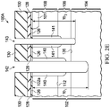
- FIGS. 2A-2G show a manufacturing process depicting cross-sectional views of the semiconductor device 100A with the due-trench configuration according to an aspect of example embodiments.
- the buried layer 106 and the upper semiconductor layer 108 are formed on the lower semiconductor layer 104.
- the buried layer 106 and the upper semiconductor layer 108 may be formed by implanting N-type dopants into the P-type lower semiconductor layer 104, followed by a thermal drive and a subsequent epitaxial process to grow the P-type upper semiconductor layer 108, so that the buried layer 106 is formed by diffusion and activation of the implanted N-type dopants.
- a transistor well region 101 is formed within the upper semiconductor layer 108 and above the buried layer 106.
- a pad oxide layer 126 is formed at the top surface 102a of the substrate 102, such as by thermal oxidation.
- the pad oxide layer 126 may include 5 nanometers to 30 nanometers of silicon dioxide.
- a pad nitride layer 128 is formed on the pad oxide layer 126, such as by low pressure chemical vapor deposition (LPCVD) using ammonia and silane.
- the pad nitride layer 128 may include 100 nanometers to 300 nanometers of silicon nitride.
- a hard mask oxide layer 130 is formed over the pad nitride layer 128, such as by a plasma enhanced chemical vapor deposition (PECVD) using tetraethyl orthosilicate, which is also known as tetraethoxysilane (TEOS), or using a high density plasma (HDP) process.
- PECVD plasma enhanced chemical vapor deposition
- TEOS tetraethoxysilane
- HDP high density plasma
- the hard mask oxide layer 130 may include 500 nanometers to 2 microns of silicon dioxide.
- the pad nitride layer 128 provides an etch stop layer for subsequent etching of the hard mask oxide layer 130.
- a trench mask 132 is formed over the hard mask oxide layer 130 so as to expose areas for forming the first deep trench structure 114 and the second deep trench structure 174 as shown and described in FIGS. 1C and ID. More specifically, the trench mask 132 is patterned with a first aperture API and a second aperture AP2.
- the first aperture API defines the first trench width 120
- the second aperture AP2 defines the second trench width 180. Accordingly, the first aperture API is generally bigger than the second aperture AP2.
- the second aperture AP2 ranges from 1.5 um to 1.8 um, whereas the first aperture API is about (e.g., +/- 10% margin) 2.65 um.
- the second aperture AP2 is about (e.g., +/- 10% margin) 1.7 um
- the first aperture API is about (e.g., +/- 10% margin) 2.65 um.
- the trench mask 132 may include a photoresist material formed by a photolithographic process, and may further include a hard mask layer and/or an anti-reflection layer.
- a hard mask etch process removes material from the hard mask oxide layer 130 in the areas exposed by the trench mask 132.
- the hard mask etch process may include a reactive ion etch (RIE) process using fluorine radicals, and/or may include a wet etch process using a dilute buffered aqueous solution of hydrofluoric acid.
- RIE reactive ion etch
- a portion of the pad nitride layer 128 may be removed by the hard mask etch process, as depicted in FIG. 2B .
- a portion or all of the trench mask 132 may be eroded by the hard mask etch process.
- a stop layer etch process removes the pad nitride layer 128 and the pad oxide layer 126 in the areas exposed by the trench mask 132.
- the stop layer etch process may include an RIE process with a different combination of gases from the hard mask etch process described in reference to FIG. 2B .
- the trench mask 132 may be further eroded by the stop layer etch process.
- the stop layer etch includes a first trench etch process removing material from the substrate 102 in the areas exposed by the trench mask 132 to simultaneously form a first partial deep trench 134 and a second partial deep trench 138.
- the first partial deep trench 134 extends to the buried layer 106 deeper than the second partial deep trench 138 given the first aperture API is wider than the second aperture AP2.
- the first trench etch process may include a continuous etch process which simultaneously removes material from the bottoms of the first and second partial deep trenches 134 and 138, and passivates sidewalls of the first and second partial deep trenches 134 and 138.
- the first deep trench etch process may include a two-step process.
- the first deep trench etch process removes material from the bottoms of the first and second partial deep trenches 134 and 138.
- the first deep trench etch process removes passivates sidewalls of the first and second partial deep trenches 134 and 138.
- the trench mask 132 may be further eroded by the first trench etch process.
- N-type dopants 139 are implanted into the substrate 102 along the sidewalls of the first partial deep trench 134 to form the first N-type sinker implanted layers 140 and along the sidewalls of the second partial deep trench 138 to form the second N-type sinker implanted layers 141.
- the N-type dopants 139 may be implanted in multiple sub-doses at tilt angles. In one example implementation, the tilt angles range from 10 degrees to 30 degrees to provide continuous coverage of the first and second sinker implanted layers 140 and 141 along the respective sidewalls of the first and second partial deep trenches 134 and 138.
- the N-type dopants 139 may also be implanted at twist angles of about 45 degrees to reduce the amount of the N-type dopants 139 implanted into bottom surfaces of the first and second partial deep trenches 134 and 138.
- An example implant process may include four sub-doses rotated at 90 degrees apart, at tilt angles of 10 degrees to 30 degrees, and at twist angles of 45 degrees. Reducing the amount of the N-type dopants 139 implanted into bottom surfaces of the first and second partial deep trench 134 and 138 may advantageously improve the process margin of a second trench etch process subsequent to the first trench etch process.
- the N-type dopants 139 may be implanted at a total dose of 1 ⁇ 10 14 cm -2 to 2 ⁇ 10 15 cm -2 so as to provide desirably low resistance of the subsequent formed sinkers.
- the N-type dopants 139 may include phosphorus and/or arsenic.
- a pad oxide layer (not shown) may be formed on the sidewalls of the first and second partial deep trenches 134 and 138. If N-type dopants 139 include arsenic, a pad oxide layer of 30 nanometers of silicon dioxide formed by a PECVD process using TEOS may improve retention of the implanted arsenic in the first and second sinker implanted layers 140 and 141.
- a pad oxide on the sidewalls of the first and second partial deep trench 134 and 138 may be omitted because the pad oxide may increases stress in the substrate 102, which may lead to degrading performance of the semiconductor device 100A.
- Implanting the n-type dopants 139 after forming the first and second partial deep trenches 134 and 138 and before forming full deeper trenches therefrom may advantageously prevent the first and second sinker implanted layers 140 and 141 from extending beyond the buried layer 106. Such a process may also improve a breakdown voltage of the PN junctions in the semiconductor device 100A.
- the first and second partial deep trenches 134 and 138 serve as a self-alignment means for forming the first and second sinker implanted layers 140 and 141, such that no additional mask is required. Because the first aperture API is wider than the second aperture AP2, the first sinker implanted layer 140 has a greater lateral thickness than the second sinker implanted layer 141.
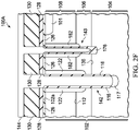
- a second trench etch process is performed to remove additional material from the substrate 102 so as to further extend the first and second partial deep trenches 134 and 138 to simultaneously form a first and second full deep trenches 142 and 143 respectively.
- the first full trench 142 has a first trench depth TD 1 greater than a second trench depth TD 2 of the second full trench 143.
- the first full trench 142 extends below the buried layer 106 by at least 17 um whereas the second full trench 143 extends below the buried layer 106 by less than 17 um.
- the first full trench 142 extends below the buried layer 106 whereas the second full trench 143 does not extend below the buried layer 106.
- a dielectric deposition process is performed to form first and second dielectric liners 116 and 176 on the sides and bottoms of the first and second full deep trenches 142 and 143 respectively.
- the dielectric liners 116 and 176 may each have a thickness ranges from 100 nanometers to 800 nanometers.
- the first and second dielectric liners 116 and 176 may include a thermal oxide layer having a thickness ranges from 200 nanometers to 300 nanometers on the sides and bottoms of the first and second full deep trenches 142 and 143.
- a silicon dioxide layer having a thickness ranges from 300 nanometers to 500 nanometers may be formed on the thermal oxide by a sub-atmospheric chemical vapor deposition (SACVD) process.
- SACVD sub-atmospheric chemical vapor deposition
- the second dielectric layer 176 forms a pinch off section 177 around the bottom portion of the second full deep trench 143, while the first dielectric layer 116 forms a relatively uniform thickness around the bottom portion of the first full deep trench 142.
- the pinch off section 177 in the second full deep trench 142 is thicker than the first dielectric layer 116 around the bottom portion of the first full deep trench 142.
- an oxide etch process is performed to create a bottom opening within the first full deep trench 142 for accessing the lower semiconductor layer 104. Because of the thicker pinch off section 177, the bottom portion of the second full deep trench 143 remains closed to the lower semiconductor layer 104 after the oxide etch process is completed.
- a P-type doping process may be performed to create a contact doped region 117 directly under the bottom opening.
- a layer of trench fill material 144 is formed in the first and second full deep trenches 142 and 143 on the first and second dielectric liners 116 and 176.
- the layer of trench fill material 144 may include a polysilicon material that fills in the first and second full deep trenches 142 and 143, and covers the hard mask oxide layer 130.
- the layer of trench fill material 144 may include silicon dioxide or other dielectric material for filling the second full deep trench 143 where the second deep trench 174 is configured to a floating state.
- first and second dielectric liners 116 and 176, and the trench fill material 144 cause the implanted N-type dopants in the first and second sinker implanted layers 140 and 141 to diffuse and become activated.
- the first and second sinkers 122 and 182 are formed without requiring a separate annealing process.
- the hard mask oxide layer 130 and the overlying portion of the layer of trench fill material 144 are subsequently removed, such as by a chemical mechanical polish (CMP) process.
- CMP chemical mechanical polish
- the first trench fill material 118 is left in the first deep trench structure 114, while the second trench fill material 178 is left in the second deep trench structure 174.
- the pad nitride layer 128 serves as an etch stop layer for removal of the hard mask oxide layer 130.
- the pad nitride layer 128 and the pad oxide layer 126 are subsequently removed, to result in the structure as shown in FIGS. 1C and ID.
- a first resistor may have a first resistance that is substantially equal to a second resistance of the second resistor, where the first and second resistors are purported to have the same resistance, yet the fabrication process introduces slight variations between the first resistance and the second resistance.
- the first resistance can be substantially equal to the second resistance, even when the fabricated first and second resistors demonstrate a slight difference in resistance. This slight difference may be within 5% of the design target.
- a first resistor may have a first resistance that is substantially equal to a second resistance of a second resistor, where the process variations are known a priori, such that the first resistance and the second resistance can be preset at slightly different values to account for the known process variations.
- the first resistance can be substantially equal to the second resistance, even when the design values of the first and second resistance are preset to include a slight difference to account for the known process variations. This slight difference may be within 5% of the design target.
- the term “configured to” describes structural and functional characteristics of one or more tangible non-transitory components.
- a “configured to” component has a particular configuration that is designed or dedicated for performing a certain function.
- a device is “configured to” perform a recited function if the device includes tangible non-transitory components that can be enabled, activated or powered to perform that recited function.
- the term “configured to” may encompass being configurable, but it is not limited to such a narrow definition. Thus, when used for describing a device, the term “configured to” does not require the described device to be configurable at any given point of time.
Description
- Integrated circuits with high voltage capabilities have wide industrial applications, including power management systems for use in automobiles. These integrated circuits include high voltage transistors that operate at a high voltage range (e.g., 80v to 120v) and low voltage transistors that operate at a much lower voltage range (e.g., 1v to 5v). To protect the low voltage transistors from the high voltage operations, an integrated circuit may adopt one or more isolation schemes. For example, one scheme involves forming a buried layer (e.g., an N-type buried layer) on top of a bulk substrate (e.g., a P-type substrate) to isolate the high voltage transistors from the low voltage transistors. The buried layer is usually biased at a high voltage corresponding to the operating range of the high voltage transistors, whereas the bulk substrate is usually biased at a ground supply voltage. In some cases, the difference between the high bias voltage and the ground supply voltage may exceed a breakdown voltage threshold of a PN junction between the buried layer and the bulk substrate, thereby causing leakages and impacting the performance and reliability of the integrated circuit.
US2013/328123 relates to a semiconductor including a first trench structure and a second trench structure.EP 1 710 834 discloses a double trench for isolation of semiconductor devices. - In described examples of systems and techniques relating to manufacturing of a semiconductor device that can handle high voltage operations alongside low voltage operations, the semiconductor device may be a standalone discrete component or incorporated as a part of an integrated circuit. The semiconductor device adopts an isolation scheme to protect low voltage transistors from high voltage operations. The described isolation scheme allows the high voltage transistors to operate at a high voltage range while reducing the voltage stress between a buried layer and a bulk substrate of the semiconductor device. Advantageously, the described isolation scheme provides a low-cost and high-performance solution to alleviate junction breakdowns of the semiconductor device.
- In one example, an integrated circuit includes a substrate, a buried layer, a transistor well region, a first trench, and a second trench. The substrate has a top surface and a bottom surface. The buried layer is positioned within the substrate, and the transistor well region is positioned above the buried layer. The first trench extends from the top surface to penetrate the buried layer, and the first trench has a first trench depth. The second trench extends from the top surface to penetrate the buried layer. The second trench is interposed between the first trench and the transistor well region. The second trench has a second trench depth that is less than the first trench depth.
- More specifically, the substrate has a first conductivity type, and the buried layer has a second conductivity type opposite of the first conductivity type. The first trench includes a first conductor that is insulated from the buried layer and making an ohmic contact with the substrate around a bottom portion of the first trench, whereas the second trench includes a second conductor insulated from the buried layer and the substrate.
- In a method of manufacturing a semiconductor device, the method includes forming a buried layer within a substrate. The method also includes forming a transistor well region above the buried layer. The method further includes forming a first trench extending from a top surface of the substrate to penetrate the buried layer, and forming a second trench extending from the top surface of the substrate to penetrate the buried layer. More specifically, the second trench is interposed between the first trench and the transistor well region, and the second trench has a trench depth less than that of the first trench. The method further includes the step of forming a first conductor within the first trench, the first conductor insulated from the buried layer and making an ohmic contact with the substrate around a bottom portion of the first trench; and the step of forming a second conductor within the second trench, the second conductor insulated from the buried layer and the substrate.
-
-
FIG. 1A shows a top view of a semiconductor device according to an aspect of example embodiments which are not part of the invention. -
FIG. 1B shows a cross-sectional view of the semiconductor device according to an aspect of example embodiments which are not part of the invention. -
FIG. 1C shows a top view of a semiconductor device with a dual-trench configuration according to an aspect of example embodiments. - FIG. ID shows a cross-sectional view of the semiconductor device with the dual-trench configuration according to an aspect of example embodiments.
-
FIGS. 2A-2G show a manufacturing process depicting cross-sectional views of the semiconductor device with the due-trench configuration according to an aspect of example embodiments. - Like reference symbols in the various drawings indicate like elements. The drawings are not drawn to scale.
-
FIG. 1A shows a top view of asemiconductor device 100, andFIG. 1B shows a cross-sectional view of thesemiconductor device 100 to illustrate its vertical structure. Thesemiconductor device 100 includes asubstrate 102, which can be subdivided into alower semiconductor layer 104 and anupper semiconductor layer 108. Thelower semiconductor layer 104 forms abottom surface 102b of thesubstrate 102, whereas theupper semiconductor layer 108 forms atop surface 102a of thesubstrate 102. For example, thelower semiconductor layer 104 may be a part of a bulk silicon substrate (e.g., 102), an epitaxial layer on a bulk silicon wafer, or a silicon-on-insulator (SOI) wafer. Theupper semiconductor layer 108 may be an epitaxial layer formed above thelower semiconductor layer 102, or as an extension of a bulk silicon substrate (e.g., 102). The lower andupper semiconductor layer - The
semiconductor device 100 includes a buriedlayer 106 positioned within thesubstrate 102. The buriedlayer 106 may be developed by doping thelower semiconductor layer 104. Alternatively, the buriedlayer 106 may be formed by growing an epitaxial layer with in situ doping on top of thelower semiconductor layer 104. The buriedlayer 106 is interposed between the lower and upper semiconductor layers 104 and 108, and the buriedlayer 106 has the opposite conductivity type from these twolayers layer 106 forms afirst PN junction 105 with thelower semiconductor layer 104 and asecond PN junction 107 with theupper semiconductor layer 108. The buriedlayer 106 may have an average doping density of at least 1 × 1018 cm-3 and commonly has an opposite conductivity type from thelower semiconductor layer 104. Atop boundary 112 of the buriedlayer 106 is at least 2 microns below thetop surface 102a of thesubstrate 102, and may extend 5 microns to 10 microns below thetop surface 102a of thesubstrate 102. The buriedlayer 106 may extend laterally across thesemiconductor device 100 as depicted inFIG. 1 , or alternatively, the buried layer may be developed or formed within a finite lateral region that is coplanar with thesubstrate 102. - The
semiconductor device 100 includes atransistor well region 101 that is positioned within theupper semiconductor layer 108 and above the buriedlayer 106. Thetransistor well region 101 includes transistors for forming one or more active circuits. In the event that thetransistor well region 101 includes a low voltage circuit (e.g., a circuit that operates with less than 10v), thetransistor well region 101 is isolated and protected from a high voltage circuit (e.g., a circuit that operates with more than 50v) formed outside of thetransistor well region 101. Alternatively, in the event that thetransistor well region 101 includes a high voltage circuit, thetransistor well region 101 is isolated to protect a low voltage circuit formed outside of thetransistor well region 101. - To isolate the high voltage circuit from the low voltage circuit, the
semiconductor device 100 includes one or moredeep trench structures 114 arranged to laterally surround thetransistor well region 101 and intersect the buriedlayer 106. More specifically, thedeep trench structure 114 extends from thetop surface 102a to penetrate through the buriedlayer 106, thereby reaching thelower semiconductor layer 104. Thedeep trench structure 114 may have atrench width 120 of less than 6 um. In one example implementation, thetrench width 120 may range from 1 micron to 4 microns. Thedeep trench structure 114 includesdielectric liners 116 disposed along the interior sidewalls. Thedielectric liners 116 may include thermal silicon dioxide. Thedeep trench structure 114 defines a bottom opening for accessing thelower semiconductor layer 104 of thesubstrate 102. The access point is doped with a dopant of the same conductivity type as thelower semiconductor layer 104 to form a dopedregion 117. In one implementation, the dopedregion 117 may have a higher doping concentration than thelower semiconductor layer 104. - The
deep trench structure 114 includestrench fill material 118 disposed onto thedielectric liners 116. Thetrench fill material 118 is conductive, and it is insulated from theupper semiconductor layer 108 and the buriedlayer 106. In one example implementation, thetrench fill material 118 includes polycrystalline silicon, which is commonly referred to as polysilicon. The trench fill material (i.e., trench conductor) 118 establishes an ohmic contact with thelower semiconductor layer 104 of thesubstrate 102 via the bottom opening and the dopedregion 117. Through this ohmic contact, thetrench conductor 118 can be used for biasing thelower semiconductor layer 104 of thesubstrate 102. In one example implementation, thetrench conductor 118 may be structured to receive a ground supply voltage VGND to bias thelower semiconductor layer 104 of thesubstrate 102. - When being biased at a voltage VBIAS corresponding to the operation voltage range of the high voltage circuit, the buried
layer 106 can be used as an isolation structure as well. For example, where the operation voltage range of the high voltage circuit is between 80v and 100v, the bias voltage VBIAS of the buriedlayer 106 may range from 100v to 170v. To bias the buriedlayer 106, thesemiconductor device 100 includes vertical doped structures (a.k.a. sinkers) 122 that extend from thetop surface 102a to reach the buriedlayer 106. Thesinkers 122 are doped with dopants of the same conductivity type as the buriedlayer 106 so as to provide electrical connections to the buriedlayer 106. In one example implementation, thesinkers 122 are doped with N-type materials where the buriedlayer 106 is N-doped as well. - For self-alignment purposes, the
sinkers 122 may be formed alongside thedeep trench structure 114. Thesinkers 122 extend laterally from thedeep trench structure 114 to have athickness 124, and thesinkers 122 coextend with thedeep trench structure 114 to provide a conductive path between thetop surface 102a and the buriedlayer 106. In one implementation, thethickness 124 of the sinkers is less than 2.5 microns, which may advantageously reduce the size of thesemiconductor device 100 when compared to semiconductor devices without self-alignment sinkers. - As shown in
FIG. 1A , thetrench structure 114 and thesinkers 122 form a contiguous ring that circumscribes thetransistor well region 101. In an alternative implementation, thetrench structure 114 and thesinkers 122 may be arranged as disconnected and discrete segments to approximate the contiguous ring for isolating thetransistor well region 101. - During operations, the
upper semiconductor layer 108 may incur a relatively high voltage where thetransistor well region 101 includes one or more high voltage circuits. For example, theupper semiconductor layer 108 may incur a voltage ranges from 80v to 100v. To prevent a current from crossing the second PN junction 107 (e.g., due to a forward bias), the buriedlayer 106 is biased with a voltage VBIAS that is higher than the voltage incurred by theupper semiconductor layer 108. In one example implementation, the bias voltage VBIAS may range from 100v to 170v. In another example implementation, the bias voltage VBIAS may range from 140v to 170v. In yet another example implementation, the bias voltage VBIAS may range from 145v to 155v. - When the
lower semiconductor layer 104 is biased at a ground supply voltage VGND, the potential difference between the buriedlayer 106 and thelower semiconductor layer 104 can become significantly large. And when this potential difference becomes larger than the breakdown voltage (e.g., less than 80v) of thefirst PN junction 105, thesemiconductor device 100 may experience a substantial amount of current leakage. This potential difference can be illustrated by an electric field density spread across a high electric field line V1 and a low electric field line V2. Generally, the high electric field line V1 represents a potential distribution closer to the bias voltage VBIAS, and the low electric field line V2 represents a potential distribution closer to the ground supply voltage VGND. The likelihood of having a breakdown at thefirst PN junction 105 is directly proportional to the potential difference between V1 and V2, and inversely proportional to a distance between V1 and V2. - According to an aspect of example embodiments not part of the invention, thickening the
dielectric liner 116 may help increase the low electric field line V2 as the ground potential carried by thetrench conductor 118 exerts less capacitive coupling to the adjacent P-region of thelower semiconductor layer 104. By increasing the low electric field line V2, the potential difference between V1 and V2 can be reduced to lower the likelihood of having a breakdown along thefirst PN junction 105. This approach may be less effective where V1 is substantially higher than V2 (e.g., V1 - V2 ≥ 100v) and the maximum thickness of thedielectric liner 116 is limited by one or more process parameters. - According to another aspect of example embodiments not part of the invention, increasing the thickness of the buried layer 106 (e.g., thickness of the buried layer ≥ 12 um) may help reduce the electric field density between V1 and V2 to avoid electric field crowding along the
first PN junction 105. By reducing the electric field density, the potential gradient at thefirst PN junction 105 can be reduced to lower the likelihood of having a breakdown along thefirst PN junction 105. This approach may be costly where V1 is substantially higher than V2 (e.g., V1 - V2 ≥ 100v) because a thickened buriedlayer 106 usually requires more material and time to develop, and it can be more difficult to etch in forming thedeep trench structure 114. - According to yet another aspect of example embodiments not part of the invention, the buried
layer 106 may include an upper buriedlayer 106a with a first doping concentration and a lower buriedlayer 106b with a second doping concentration that is lower than the first doping concentration. For example, the upper buriedlayer 106a may have a doping concentration that is greater than 5×1018 cm-3, whereas the lower buriedlayer 106b may have a doping concentration ranging from 1×1016 cm-3 to 1×1017 cm-3. By adjusting the doping profile within the buriedlayer 106, the potential gradient across thefirst PN junction 105 can be reduced to lower the likelihood of having a breakdown. This approach may be less effective where V1 is substantially higher than V2 (e.g., V1 - V2 ≥ 100v) and the maximum thickness of the buriedlayer 106 is limited (e.g., maximum thickness ≤ 12 um). - To address the constraints described hereinabove, example embodiments introduce a dual-trench configuration that alleviates electric field crowding around the
first PN junction 105 between the buriedlayer 106 and thelower semiconductor layer 104 of thesubstrate 102.FIG. 1C shows a top view of asemiconductor device 100A with a dual-trench configuration, and FIG. ID shows a cross-sectional view of thesemiconductor device 100A according to an aspect of example embodiments. Thesemiconductor device 100A is similar to thesemiconductor device 100 to the extent that these two devices include components identified with the same numeric labels. Thesemiconductor device 100A differs from thesemiconductor device 100 in that thesemiconductor device 100A includes a seconddeep trench structure 174. - The second
deep trench structure 174 is arranged to laterally surround thetransistor well region 101 and intersect the buriedlayer 106. More specifically, the seconddeep trench structure 174 extends from thetop surface 102a to penetrate the buriedlayer 106. In one example implementation, the seconddeep trench structure 174 may penetrate through the buriedlayer 106 to reach thelower semiconductor layer 104 of thesubstrate 102. In another example implementation, the seconddeep trench structure 174 may partially penetrate the buriedlayer 106 and terminate within the buriedlayer 106. The seconddeep trench structure 174 is interposed between the firstdeep trench structure 114 and thetransistor well region 101. As shown inFIG. 1C , the seconddeep trench structure 174 circumscribes thetransistor well region 101, while being circumscribed by the firstdeep trench structure 114. Together, thedual trenches transistor well region 101. In an alternative implementation, each of the first and seconddeep trench structures transistor well region 101. - To facilitate an efficient etching process and an efficient dielectric filing process, the second
deep trench structure 174 may be formed concurrently with the firstdeep trench structure 114. To that end, the seconddeep trench structure 174 may have a second trench width (i.e., second trench aperture) 180 that is less than the first trench width (i.e., first trench aperture) 120 of the firstdeep trench structure 114. In one example implementation, thesecond trench width 180 ranges from 1.5 um to 1.8 um, whereas thefirst trench width 120 is about (e.g., +/- 10% margin) 2.65 um. In another example implementation, thesecond trench width 180 is about (e.g., +/- 10% margin) 1.7 um, whereas thefirst trench width 120 is about (e.g., +/- 10% margin) 2.65 um. - Due to the difference in trench widths, the first
deep trench structure 114 has a first trench depth TD1 that is greater than a second trench depth TD2 of the seconddeep trench structure 174 when they are simultaneously etched for the same amount of time. In one example implementation, the first trench depth TD1 ranges from 20 um to 28 um, whereas the second trench depth TD2 ranges from 8 um to 16 um. In another example implementation, the first trench depth TD1 ranges from 23 um to 27 um, whereas the second trench depth TD2 ranges from 13 um to 15 um. In yet another example implementation, the first trench depth TD1 is about (e.g., +/- 10% margin) 24 um, whereas the second trench depth TD2 is about (e.g., +/- 10% margin) 14 um. - Alternatively, the second
deep trench structure 174 may have asecond trench width 180 that is substantially the same (e.g., +/- 5% margin) as thefirst trench width 120 of the firstdeep trench structure 114. Under this particular configuration, the first trench depth TD1 may be substantially the same (e.g., +/- 5% margin) as the second trench depth TD2. In one example implementation, each of the first and second trench depths TD1 and TD2 ranges from 20 um to 28 um. In another example implementation, each of the first and second trench depths TD1 and TD2 ranges from 23 um to 27 um. In yet another example implementation, each of the first and second trench depths TD1 and TD2 is about (e.g., +/- 10% margin) 24 um. - Similar to the first
deep trench structure 114, the seconddeep trench structure 174 includesdielectric liners 176 disposed along the sidewalls and a bottom portion of thereof. Thedielectric liners 176 may include thermal silicon dioxide. Thedielectric liner 176 seals off the seconddeep trench structure 174 to prevent any access to thelower semiconductor layer 104 of thesubstrate 102. When thesecond trench width 180 is smaller than thefirst trench width 120, a simultaneous dielectric formation process may cause thedielectric liners 176 to be slightly sloped and thicker around the bottom portion of the seconddeep trench structure 174. - The second
deep trench structure 174 includestrench fill material 178 disposed onto thedielectric liners 176. Thetrench fill material 178 is conductive where the seconddeep trench structure 174 is configured to receive a trench bias voltage VTR. Thetrench fill material 178 is conductive also where the seconddeep trench structure 174 is configured to a floating state. In a configuration where thetrench fill material 178 is conductive, thetrench conductor 178 is insulated from theupper semiconductor layer 108, the buriedlayer 106, and thelower semiconductor layer 104. In one example implementation, thetrench fill material 178 includes polycrystalline silicon, which is commonly referred to as polysilicon. Unlike thetrench fill conductor 118, thetrench fill conductor 178 does not establish any ohmic contact with thelower semiconductor layer 104 of thesubstrate 102. Rather, thetrench fill conductor 178 establishes a capacitive coupling with the buriedlayer 106 and thelower semiconductor layer 104. Through this capacitive coupling, thetrench conductor 178 can be used for influencing the electric field density of the buriedlayer 106, and thelower semiconductor layer 104 of thesubstrate 102. In one example implementation, thetrench conductor 178 may be structured to receive a trench bias voltage VTR to reduce the electric field density around thefirst PN junction 105 between the buriedlayer 106 and thelower semiconductor layer 104. - Similar to the
semiconductor device 100, thesemiconductor device 100A includes vertical doped structures (a.k.a. sinkers) 182. Thesinkers 182 serve as a conduit for biasing the buriedlayer 106 to a bias voltage VBIAS, thereby establishing a reverse bias between the P-typeupper semiconductor layer 108 and the N-type buriedlayer 106. Thesinkers 182 extend from thetop surface 102a to reach the buriedlayer 106. Thesinkers 182 are doped with dopants of the same conductivity type as the buriedlayer 106 so as to provide electrical connections to the buriedlayer 106. In one example implementation, thesinkers 182 are doped with N-type materials where the buriedlayer 106 is N-doped as well. - For self-alignment purposes, the
sinkers 182 may be formed alongside the seconddeep trench structure 174. Thesinkers 182 extend laterally from the seconddeep trench structure 174 to have athickness 184, and thesinkers 182 coextend with the seconddeep trench structure 174 to provide a conductive path between thetop surface 102a and the buriedlayer 106. In one implementation, thethickness 184 of the sinkers may be less than 2.5 microns, which may advantageously reduce the size of thesemiconductor device 100 when compared to semiconductor devices without self-alignment sinkers. When thesecond trench width 180 is less than thefirst trench width 120, thesecond sinker thickness 184 may be less than thefirst sinker thickness 124. - The dual-trench configuration provides several advantages over the single-trench configuration in sustaining a high operation voltage range while preventing breakdowns around an isolation junction. The first advantage includes widening the electric field line distributions between the high electric field line V1 and the low electric field line V2. The widened distribution reduces the potential difference around the
first PN junction 105. For example, as shown in FIG. ID, the high electric field line V1 and the low electric field line V2 are spaced further apart, such that the potential difference across thefirst PN junction 105 may be substantially reduced. - The widened distribution of electric field lines can be attributed to the structural features of the second
deep trench structure 174. In one aspect, by not establishing any ohmic contact with, and thus not biasing, thesubstrate 102, the seconddeep trench structure 174 helps sustain a relatively low potential difference across thefirst PN junction 105 around a region surrounding the seconddeep trench structure 174. In another aspect, the seconddeep trench structure 174 helps reduce the potential difference across thefirst PN junction 105 by having a thickerdielectric liner 178 around the bottom portion thereof. In yet another aspect, the relative positioning of the seconddeep trench structure 174 helps spread the electric field lines between thebiased sinker 182 and the floatingsinkers 182' and 122. By virtue of being interposed between the first deep trench structure 114 (which is configured to carry a ground supply voltage VGND (e.g., 0v)) and the biased region of the buried layer 106 (which is biased at a high bias voltage VBIAS (e.g., 100v - 170v)), the seconddeep trench structure 174 serves as a voltage buffer between these two regions. - The inter-trench distance dT between the first
deep trench structure 114 and the seconddeep trench structure 174 is associated with a breakdown voltage of thefirst PN junction 105 between the buriedlayer 106 and thelower semiconductor layer 104 of thesubstrate 102. Generally, the breakdown voltage is inversely proportional to the inter-trench distance dT. In one example implementation, an inter-trench distance dT of at least 1 um may be sufficient to prevent junction breakdown of thefirst PN junction 105 where the breakdown voltage of 100v or lower. In another example implementation, an inter-trench distance dT of about (e.g., +/- 10% margin) 1.5 um may be sufficient to prevent junction breakdown of thefirst PN junction 105 where the breakdown voltage is about (e.g., +/- 10% margin) 80v. - The inter-trench distance dT may also be associated with an electric field density threshold of the
first PN junction 105 between the buriedlayer 106 and thelower semiconductor layer 104 of thesubstrate 102. Assuming thesemiconductor device 100A has an electric field density of 10v/um, the inter-trench distance dT is about (e.g., +/- 10 % margin) 2um to sustain a 20v potential difference between the high electric field line V1 and the low electric field line V2. Similarly, assuming thesemiconductor device 100A has an electric field density threshold of 20v/um , the inter-trench distance dT is about (e.g., +/- 10 % margin) 1um to sustain a 20v potential difference between the high electric field line V1 and the low electric field line V2. Under these assumptions, the inter-trench distance dT is inversely proportional to the electric field density threshold of thefirst PN junction 105. - The second advantage of the dual-trench configuration includes lowering the a potential spectrum across the high electric field line V1 and the low electric field line V2. In an implementation where the second
trench fill material 178 is conductive, the seconddeep trench structure 174 can be configured to receive a trench bias voltage VTR. The trench bias voltage VTR may lower the value of the high electric field line V2 relative to the bias voltage VBIAS as applied to the buriedlayer 106. In one example, the high electric field line V2 may be reduced to 100v where the bias voltage VBIAS is set to 140v and the trench bias voltage VTR is set to 40v. Similarly, the high electric field line V2 may be reduced to 80v where the bias voltage VBIAS is set to 140v and the trench bias voltage VTR is set to 60v. - To avoid junction breakdowns, the trench bias voltage VTR can be associated with a breakdown voltage of the
first PN junction 105 between the buriedlayer 106 and thelower semiconductor layer 104 of thesubstrate 102. In one example implementation, the trench bias voltage VTR can be set to 40v where the breakdown voltage is 80v and the buried layer bias voltage VBIAS is less than 120v. In another example implementation, the trench bias voltage VTR can be set to 60v where the break down voltage is 60v and the buried layer bias voltage VBIAS is less than 120v. Under these examples, the trench bias voltage VTR is inversely proportional to the breakdown voltage of thefirst PN junction 105 between the buriedlayer 106 and thelower semiconductor layer 104 of thesubstrate 102. - And to avoid electric field crowding, the trench bias voltage VTR can also be associate with an electric field density threshold of the
first PN junction 105 between the buriedlayer 106 and thelower semiconductor layer 104 of thesubstrate 102. Assuming thesemiconductor device 100A has an electric field density of 10v/um and an inter-trench distance dT of 2um, the trench bias voltage VTR can be set to 40v to sustain a 80v potential difference between the high electric field line V1 and the low electric field line V2 where the buried layer bias voltage VBIAS is at 140v. Similarly, assuming thesemiconductor device 100A has an electric field density of 20v/um and an inter-trench distance dT of 2um, the trench bias voltage VTR can be set to 20v to sustain a 80v potential difference between the high electric field line V1 and the low electric field line V2 where the buried layer bias voltage VBIAS is at 140v.. Under these assumptions, the trench bias voltage VTR is inversely proportional to the electric field density threshold of thefirst PN junction 105. -
FIGS. 2A-2G show a manufacturing process depicting cross-sectional views of thesemiconductor device 100A with the due-trench configuration according to an aspect of example embodiments. Referring toFIG. 2A , the buriedlayer 106 and theupper semiconductor layer 108 are formed on thelower semiconductor layer 104. The buriedlayer 106 and theupper semiconductor layer 108 may be formed by implanting N-type dopants into the P-typelower semiconductor layer 104, followed by a thermal drive and a subsequent epitaxial process to grow the P-typeupper semiconductor layer 108, so that the buriedlayer 106 is formed by diffusion and activation of the implanted N-type dopants. After theupper semiconductor layer 108 is formed, atransistor well region 101 is formed within theupper semiconductor layer 108 and above the buriedlayer 106. - A
pad oxide layer 126 is formed at thetop surface 102a of thesubstrate 102, such as by thermal oxidation. Thepad oxide layer 126 may include 5 nanometers to 30 nanometers of silicon dioxide. Apad nitride layer 128 is formed on thepad oxide layer 126, such as by low pressure chemical vapor deposition (LPCVD) using ammonia and silane. Thepad nitride layer 128 may include 100 nanometers to 300 nanometers of silicon nitride. A hardmask oxide layer 130 is formed over thepad nitride layer 128, such as by a plasma enhanced chemical vapor deposition (PECVD) using tetraethyl orthosilicate, which is also known as tetraethoxysilane (TEOS), or using a high density plasma (HDP) process. The hardmask oxide layer 130 may include 500 nanometers to 2 microns of silicon dioxide. Thepad nitride layer 128 provides an etch stop layer for subsequent etching of the hardmask oxide layer 130. - A
trench mask 132 is formed over the hardmask oxide layer 130 so as to expose areas for forming the firstdeep trench structure 114 and the seconddeep trench structure 174 as shown and described inFIGS. 1C and ID. More specifically, thetrench mask 132 is patterned with a first aperture API and a second aperture AP2. The first aperture API defines thefirst trench width 120, whereas the second aperture AP2 defines thesecond trench width 180. Accordingly, the first aperture API is generally bigger than the second aperture AP2. In one example implementation, the second aperture AP2 ranges from 1.5 um to 1.8 um, whereas the first aperture API is about (e.g., +/- 10% margin) 2.65 um. In another example implementation, the second aperture AP2 is about (e.g., +/- 10% margin) 1.7 um, whereas the first aperture API is about (e.g., +/- 10% margin) 2.65 um. Thetrench mask 132 may include a photoresist material formed by a photolithographic process, and may further include a hard mask layer and/or an anti-reflection layer. - Referring to
FIG. 2B , a hard mask etch process removes material from the hardmask oxide layer 130 in the areas exposed by thetrench mask 132. The hard mask etch process may include a reactive ion etch (RIE) process using fluorine radicals, and/or may include a wet etch process using a dilute buffered aqueous solution of hydrofluoric acid. A portion of thepad nitride layer 128 may be removed by the hard mask etch process, as depicted inFIG. 2B . A portion or all of thetrench mask 132 may be eroded by the hard mask etch process. - Referring to
FIG. 2C , a stop layer etch process removes thepad nitride layer 128 and thepad oxide layer 126 in the areas exposed by thetrench mask 132. The stop layer etch process may include an RIE process with a different combination of gases from the hard mask etch process described in reference toFIG. 2B . Thetrench mask 132 may be further eroded by the stop layer etch process. - The stop layer etch includes a first trench etch process removing material from the
substrate 102 in the areas exposed by thetrench mask 132 to simultaneously form a first partialdeep trench 134 and a second partialdeep trench 138. The first partialdeep trench 134 extends to the buriedlayer 106 deeper than the second partialdeep trench 138 given the first aperture API is wider than the second aperture AP2. The first trench etch process may include a continuous etch process which simultaneously removes material from the bottoms of the first and second partialdeep trenches deep trenches deep trenches deep trenches trench mask 132 may be further eroded by the first trench etch process. - Referring to
FIG. 2D , N-type dopants 139 are implanted into thesubstrate 102 along the sidewalls of the first partialdeep trench 134 to form the first N-type sinker implantedlayers 140 and along the sidewalls of the second partialdeep trench 138 to form the second N-type sinker implanted layers 141. The N-type dopants 139 may be implanted in multiple sub-doses at tilt angles. In one example implementation, the tilt angles range from 10 degrees to 30 degrees to provide continuous coverage of the first and second sinker implantedlayers deep trenches - The N-
type dopants 139 may also be implanted at twist angles of about 45 degrees to reduce the amount of the N-type dopants 139 implanted into bottom surfaces of the first and second partialdeep trenches type dopants 139 implanted into bottom surfaces of the first and second partialdeep trench - The N-
type dopants 139 may be implanted at a total dose of 1 × 1014 cm-2 to 2 × 1015 cm-2 so as to provide desirably low resistance of the subsequent formed sinkers. The N-type dopants 139 may include phosphorus and/or arsenic. A pad oxide layer (not shown) may be formed on the sidewalls of the first and second partialdeep trenches type dopants 139 include arsenic, a pad oxide layer of 30 nanometers of silicon dioxide formed by a PECVD process using TEOS may improve retention of the implanted arsenic in the first and second sinker implantedlayers type dopants 139 do not include arsenic, a pad oxide on the sidewalls of the first and second partialdeep trench substrate 102, which may lead to degrading performance of thesemiconductor device 100A. - Implanting the n-
type dopants 139 after forming the first and second partialdeep trenches layers layer 106. Such a process may also improve a breakdown voltage of the PN junctions in thesemiconductor device 100A. Moreover, the first and second partialdeep trenches layers layer 140 has a greater lateral thickness than the second sinker implantedlayer 141. - Referring to
FIG. 2E , a second trench etch process is performed to remove additional material from thesubstrate 102 so as to further extend the first and second partialdeep trenches deep trenches full trench 142 has a first trench depth TD1 greater than a second trench depth TD2 of the secondfull trench 143. In one example implementation, the firstfull trench 142 extends below the buriedlayer 106 by at least 17 um whereas the secondfull trench 143 extends below the buriedlayer 106 by less than 17 um. In another example implementation, the firstfull trench 142 extends below the buriedlayer 106 whereas the secondfull trench 143 does not extend below the buriedlayer 106. Upon the completion of the second trench etch process, substantially all of the remainingtrench mask 132. - Referring to
FIG. 2F , a dielectric deposition process is performed to form first and seconddielectric liners deep trenches dielectric liners dielectric liners deep trenches - Because the first deep
full trench 142 has a greater trench width than the second fulldeep trench 143, thesecond dielectric layer 176 forms a pinch off section 177 around the bottom portion of the second fulldeep trench 143, while thefirst dielectric layer 116 forms a relatively uniform thickness around the bottom portion of the first fulldeep trench 142. Generally, the pinch off section 177 in the second fulldeep trench 142 is thicker than thefirst dielectric layer 116 around the bottom portion of the first fulldeep trench 142. - Next, an oxide etch process is performed to create a bottom opening within the first full
deep trench 142 for accessing thelower semiconductor layer 104. Because of the thicker pinch off section 177, the bottom portion of the second fulldeep trench 143 remains closed to thelower semiconductor layer 104 after the oxide etch process is completed. Upon creating the bottom opening within the first fulldeep trench 142, a P-type doping process may be performed to create a contact dopedregion 117 directly under the bottom opening. - Then, a layer of
trench fill material 144 is formed in the first and second fulldeep trenches dielectric liners trench fill material 144 may include a polysilicon material that fills in the first and second fulldeep trenches mask oxide layer 130. Alternatively, the layer oftrench fill material 144 may include silicon dioxide or other dielectric material for filling the second fulldeep trench 143 where the seconddeep trench 174 is configured to a floating state. - Thermal profiles during formation of the first and second
dielectric liners trench fill material 144, cause the implanted N-type dopants in the first and second sinker implantedlayers second sinkers - Referring to
FIG. 2G , the hardmask oxide layer 130 and the overlying portion of the layer oftrench fill material 144 are subsequently removed, such as by a chemical mechanical polish (CMP) process. As a result, the firsttrench fill material 118 is left in the firstdeep trench structure 114, while the secondtrench fill material 178 is left in the seconddeep trench structure 174. Thepad nitride layer 128 serves as an etch stop layer for removal of the hardmask oxide layer 130. Thepad nitride layer 128 and thepad oxide layer 126 are subsequently removed, to result in the structure as shown inFIGS. 1C and ID. - In this description, the terms "substantially equal to," "substantially equal," "substantially the same" and variations thereof, as applied to features of an integrated circuit, mean equal within fabrication tolerances to form the integrated circuit. More specifically, the terms "substantially equal to" and "substantially equals" describe a quantitative relationship between two objects. This quantitative relationship may prefer the two objects to be equal by design, but with the anticipation that a certain amount of variations can be introduced by the fabrication process. In one aspect, a first resistor may have a first resistance that is substantially equal to a second resistance of the second resistor, where the first and second resistors are purported to have the same resistance, yet the fabrication process introduces slight variations between the first resistance and the second resistance. Thus, the first resistance can be substantially equal to the second resistance, even when the fabricated first and second resistors demonstrate a slight difference in resistance. This slight difference may be within 5% of the design target. In another aspect, a first resistor may have a first resistance that is substantially equal to a second resistance of a second resistor, where the process variations are known a priori, such that the first resistance and the second resistance can be preset at slightly different values to account for the known process variations. Thus, the first resistance can be substantially equal to the second resistance, even when the design values of the first and second resistance are preset to include a slight difference to account for the known process variations. This slight difference may be within 5% of the design target.
- In this description, the term "configured to" describes structural and functional characteristics of one or more tangible non-transitory components. For example, a "configured to" component has a particular configuration that is designed or dedicated for performing a certain function. Accordingly, a device is "configured to" perform a recited function if the device includes tangible non-transitory components that can be enabled, activated or powered to perform that recited function. The term "configured to" may encompass being configurable, but it is not limited to such a narrow definition. Thus, when used for describing a device, the term "configured to" does not require the described device to be configurable at any given point of time.
- Similarly, although operations are depicted in the drawings in a particular order, such operations are not required to be performed in the particular order shown or in sequential order (and not all illustrated operations are required to be performed) to achieve desirable results, unless such order is recited as being required. In certain circumstances, simultaneous processing may be advantageous for fabricating multiple structures of a semiconductor device. Moreover, the separation of various system components in the embodiments described hereinabove does not require such separation in all embodiments.
Claims (16)
- An integrated circuit, comprising:a substrate (102) having a top surface (102a) and a bottom surface (102b);a buried layer (106) positioned within the substrate;a transistor well region (101) positioned above the buried layer;a first trench (114) extending from the top surface to penetrate the buried layer, the first trench having a first trench depth (TD1); anda second trench (174) extending from the top surface to penetrate the buried layer, the second trench interposed between the first trench and the transistor well region, and having a second trench depth (TD2) less than the first trench depth, characterised in that:the first trench includes a first conductor (118) insulated from the buried layer and making an ohmic contact with the substrate around a bottom portion of the first trench; andthe second trench includes a second conductor (178) insulated from the buried layer and the substrate.
- The integrated circuit of claim 1, wherein the second trench includes the second conductor and a dielectric liner (176) insulating the second conductor to a floating state.
- The integrated circuit of claim 1, wherein the second trench includes the second conductor structured to receive a bias voltage associated with a breakdown voltage of a junction between the buried layer and the substrate.
- The integrated circuit of claim 1, wherein the second trench includes the second conductor structured to receive a bias voltage associated with an electric field density threshold of a junction between the buried layer and the substrate.
- The integrated circuit of claim 1, wherein the first trench is spaced apart from the second trench by a distance associated with a breakdown voltage of a junction between the buried layer and the substrate.
- The integrated circuit of claim 1, wherein the first trench is spaced apart from the second trench by a distance associated with an electric field density threshold of a junction between the buried layer and the substrate.
- The integrated circuit of claim 1, wherein the first trench is spaced apart from the second trench by a distance greater than 1 um.
- The integrated circuit of claim 1, wherein the first trench has a first aperture (120) defined at the top surface, and the second trench has a second aperture (180) defined at the top surface and smaller than the first aperture.
- The integrated circuit of claim 1, further comprising:a high voltage circuit developed outside of the transistor well region; anda low voltage circuit developed within of the transistor well region and shielded from the high voltage circuit by the first trench and the second trench.
- A method, comprising:forming a buried layer (106) within a substrate;forming a transistor well region (101) above the buried layer;forming a first trench (114) extending from a top surface of the substrate to penetrate the buried layer, the first trench having a first trench depth (TD1);forming a second trench (174) extending from the top surface of the substrate to penetrate the buried layer, the second trench interposed between the first trench and the transistor well region, and having a second trench depth (TD2) less than the first trench depth; and characterised in that the method further comprises:forming a first conductor (118) within the first trench, the first conductor insulated from the buried layer and making an ohmic contact with the substrate around a bottom portion of the first trench; andforming a second conductor (178) within the second trench, the second conductor insulated from the buried layer and the substrate.
- The method of claim 10, further comprising:forming the second conductor within the second trench;insulating the second conductor to a floating state.
- The method of claim 10, further comprising:forming the second conductor within the second trench;forming a contact with the second conductor for receiving a bias voltage associated with a breakdown voltage of a junction between the buried layer and the substrate.
- The method of claim 10, wherein the first trench is spaced apart from the second trench by a distance associated with a breakdown voltage of a junction between the buried layer and the substrate.
- The method of claim 10, wherein the first trench is spaced apart from the second trench by a distance a) associated with an electric field density threshold of a junction between the buried layer and the substrate; or b) greater than 1.5 um.
- The method of claim 10, wherein:
the forming the first trench includes:defining a first aperture (120) at the top surface of the substrate; andetching a top layer (108) of the substrate, the buried layer, and a bottom layer (104) of the substrate for a predetermined time period through the first aperture; andthe forming the second trench includes:defining a second aperture (180) at the top surface of the substrate, the second aperture smaller than the first aperture; andetching the top layer of the substrate, the buried layer, and the bottom layer of the substrate for the predetermined time period through the second aperture. - The integrated circuit of claim 10, further comprising:a high voltage circuit outside of the transistor well region; anda low voltage circuit within of the transistor well region and shielded from the high voltage circuit by the first trench and the second trench.
Applications Claiming Priority (2)
| Application Number | Priority Date | Filing Date | Title |
|---|---|---|---|
| US15/238,198 US9786665B1 (en) | 2016-08-16 | 2016-08-16 | Dual deep trenches for high voltage isolation |
| PCT/US2017/047151 WO2018035229A2 (en) | 2016-08-16 | 2017-08-16 | Dual deep trenches for high voltage isolation |
Publications (3)
| Publication Number | Publication Date |
|---|---|
| EP3501040A4 EP3501040A4 (en) | 2019-06-26 |
| EP3501040A2 EP3501040A2 (en) | 2019-06-26 |
| EP3501040B1 true EP3501040B1 (en) | 2022-04-27 |
Family
ID=59982153
Family Applications (1)
| Application Number | Title | Priority Date | Filing Date |
|---|---|---|---|
| EP17842059.2A Active EP3501040B1 (en) | 2016-08-16 | 2017-08-16 | Dual deep trenches for high voltage isolation |
Country Status (5)
| Country | Link |
|---|---|
| US (2) | US9786665B1 (en) |
| EP (1) | EP3501040B1 (en) |
| JP (2) | JP6936454B2 (en) |
| CN (1) | CN109564895B (en) |
| WO (1) | WO2018035229A2 (en) |
Families Citing this family (8)
| Publication number | Priority date | Publication date | Assignee | Title |
|---|---|---|---|---|
| US9786665B1 (en) * | 2016-08-16 | 2017-10-10 | Texas Instruments Incorporated | Dual deep trenches for high voltage isolation |
| US10262997B2 (en) * | 2017-09-14 | 2019-04-16 | Vanguard International Semiconductor Corporation | High-voltage LDMOSFET devices having polysilicon trench-type guard rings |
| CN111341847B (en) * | 2018-12-19 | 2023-03-28 | 联华电子股份有限公司 | Semiconductor structure and manufacturing method thereof |
| US10811543B2 (en) | 2018-12-26 | 2020-10-20 | Texas Instruments Incorporated | Semiconductor device with deep trench isolation and trench capacitor |
| US11158750B2 (en) | 2019-07-03 | 2021-10-26 | Texas Instruments Incorporated | Superlattice photo detector |
| DE112021006557T5 (en) * | 2021-01-15 | 2023-10-05 | Rohm Co., Ltd. | SEMICONDUCTOR DEVICE |
| JP2023032332A (en) * | 2021-08-26 | 2023-03-09 | ローム株式会社 | Semiconductor device |
| US20230261062A1 (en) * | 2022-02-15 | 2023-08-17 | Globalfoundries U.S. Inc. | Isolation regions for charge collection and removal |
Family Cites Families (25)
| Publication number | Priority date | Publication date | Assignee | Title |
|---|---|---|---|---|
| US4819052A (en) * | 1986-12-22 | 1989-04-04 | Texas Instruments Incorporated | Merged bipolar/CMOS technology using electrically active trench |
| JP3189743B2 (en) * | 1997-06-26 | 2001-07-16 | 日本電気株式会社 | Semiconductor integrated circuit device and method of manufacturing the same |
| US6316336B1 (en) * | 1999-03-01 | 2001-11-13 | Richard A. Blanchard | Method for forming buried layers with top-side contacts and the resulting structure |
| GB0507157D0 (en) * | 2005-04-08 | 2005-05-18 | Ami Semiconductor Belgium Bvba | Double trench for isolation of semiconductor devices |
| JP2007201220A (en) * | 2006-01-27 | 2007-08-09 | Mitsubishi Electric Corp | Semiconductor device |
| JP2008034649A (en) * | 2006-07-28 | 2008-02-14 | Sanyo Electric Co Ltd | Semiconductor device |
| EP2006900B1 (en) * | 2007-05-25 | 2020-11-18 | Semiconductor Components Industries, LLC | Deep trench isolation for power semiconductors |
| US7982282B2 (en) * | 2008-04-25 | 2011-07-19 | Freescale Semiconductor, Inc. | High efficiency amplifier with reduced parasitic capacitance |
| JP2010062377A (en) * | 2008-09-04 | 2010-03-18 | Sanyo Electric Co Ltd | Semiconductor device and manufacturing method thereof |
| US20100181639A1 (en) * | 2009-01-19 | 2010-07-22 | Vanguard International Semiconductor Corporation | Semiconductor devices and fabrication methods thereof |
| JP2011171602A (en) * | 2010-02-19 | 2011-09-01 | Oki Semiconductor Co Ltd | Semiconductor device and method of manufacturing the same |
| EP2498280B1 (en) * | 2011-03-11 | 2020-04-29 | Soitec | DRAM with trench capacitors and logic back-biased transistors integrated on an SOI substrate comprising an intrinsic semiconductor layer and manufacturing method thereof |
| FR2991502B1 (en) * | 2012-05-29 | 2014-07-11 | Commissariat Energie Atomique | METHOD FOR MANUFACTURING INTEGRATED CIRCUIT HAVING INSULATION TRENCHES WITH SEPARATE DEPTHS |
| US9159791B2 (en) * | 2012-06-06 | 2015-10-13 | United Microelectronics Corp. | Semiconductor device comprising a conductive region |
| US9343526B2 (en) * | 2013-03-13 | 2016-05-17 | Freescale Semiconductor, Inc. | Deep trench isolation |
| KR102057340B1 (en) * | 2013-03-29 | 2019-12-19 | 매그나칩 반도체 유한회사 | Semiconductor device and manufactruing method thereof |
| CN104701172B (en) * | 2013-12-05 | 2018-03-09 | 中芯国际集成电路制造(上海)有限公司 | VDMOS field-effect transistors and forming method thereof |
| US9252213B2 (en) * | 2013-12-19 | 2016-02-02 | Globalfoundries Singapore Pte. Ltd. | Integrated circuits with a buried N layer and methods for producing such integrated circuits |
| FR3021457B1 (en) * | 2014-05-21 | 2017-10-13 | St Microelectronics Rousset | COMPONENT, FOR EXAMPLE NMOS TRANSISTOR, ACTIVE REGION WITH RELEASED COMPRESSION STRESS, AND DECOUPLING CAPACITOR |
| JP6238234B2 (en) * | 2014-06-03 | 2017-11-29 | ルネサスエレクトロニクス株式会社 | Semiconductor device |
| US9660074B2 (en) * | 2014-08-07 | 2017-05-23 | Texas Instruments Incorporated | Methods and apparatus for LDMOS devices with cascaded RESURF implants and double buffers |
| US9401410B2 (en) * | 2014-11-26 | 2016-07-26 | Texas Instruments Incorporated | Poly sandwich for deep trench fill |
| US9673084B2 (en) * | 2014-12-04 | 2017-06-06 | Globalfoundries Singapore Pte. Ltd. | Isolation scheme for high voltage device |
| JP6695188B2 (en) * | 2016-03-29 | 2020-05-20 | ルネサスエレクトロニクス株式会社 | Semiconductor device and manufacturing method thereof |
| US9786665B1 (en) * | 2016-08-16 | 2017-10-10 | Texas Instruments Incorporated | Dual deep trenches for high voltage isolation |
-
2016
- 2016-08-16 US US15/238,198 patent/US9786665B1/en active Active
-
2017
- 2017-08-16 CN CN201780049630.XA patent/CN109564895B/en active Active
- 2017-08-16 JP JP2019509513A patent/JP6936454B2/en active Active
- 2017-08-16 EP EP17842059.2A patent/EP3501040B1/en active Active
- 2017-08-16 WO PCT/US2017/047151 patent/WO2018035229A2/en unknown
- 2017-08-21 US US15/681,466 patent/US10580775B2/en active Active
-
2021
- 2021-08-18 JP JP2021133052A patent/JP7293293B2/en active Active
Also Published As
| Publication number | Publication date |
|---|---|
| WO2018035229A2 (en) | 2018-02-22 |
| CN109564895A (en) | 2019-04-02 |
| JP2021184491A (en) | 2021-12-02 |
| EP3501040A4 (en) | 2019-06-26 |
| EP3501040A2 (en) | 2019-06-26 |
| JP7293293B2 (en) | 2023-06-19 |
| US10580775B2 (en) | 2020-03-03 |
| WO2018035229A3 (en) | 2018-04-05 |
| CN109564895B (en) | 2023-08-11 |
| US9786665B1 (en) | 2017-10-10 |
| JP6936454B2 (en) | 2021-09-15 |
| JP2019526932A (en) | 2019-09-19 |
| US20180053765A1 (en) | 2018-02-22 |
Similar Documents
| Publication | Publication Date | Title |
|---|---|---|
| EP3501040B1 (en) | Dual deep trenches for high voltage isolation | |
| US10163680B1 (en) | Sinker to buried layer connection region for narrow deep trenches | |
| US9917186B2 (en) | Semiconductor device with control structure including buried portions and method of manufacturing | |
| EP2706566B1 (en) | Semiconductor device and method of manufacturing same | |
| US8709895B2 (en) | Manufacturing method power semiconductor device | |
| US10672901B2 (en) | Power transistor with terminal trenches in terminal resurf regions | |
| CA2425289A1 (en) | Semiconductor structure and method for processing such a structure | |
| US8492221B2 (en) | Method for fabricating power semiconductor device with super junction structure | |
| CN103681850B (en) | Power mosfet and forming method thereof | |
| US20170110537A1 (en) | Deep trench isolation structures and systems and methods including the same | |
| JP2020129597A (en) | Semiconductor device and method of manufacturing semiconductor device | |
| US20200303539A1 (en) | Transistor Having at Least One Transistor Cell with a Field Electrode | |
| US9431286B1 (en) | Deep trench with self-aligned sinker | |
| US7923330B2 (en) | Method for manufacturing a semiconductor device | |
| US10749028B2 (en) | Transistor with gate/field plate structure | |
| TW201338049A (en) | Trench junction electric-field shielding power metal oxide semiconductor field effect transistor structure and manufacturing process method | |
| KR20230090581A (en) | Semiconductor device and method of manufacturing same | |
| KR20160092337A (en) | power metal oxide semiconductor(MOS) type diode having superjuction structure and trench gate and fabrication method thereof |
Legal Events
| Date | Code | Title | Description |
|---|---|---|---|
| STAA | Information on the status of an ep patent application or granted ep patent |
Free format text: STATUS: THE INTERNATIONAL PUBLICATION HAS BEEN MADE |
|
| PUAI | Public reference made under article 153(3) epc to a published international application that has entered the european phase |
Free format text: ORIGINAL CODE: 0009012 |
|
| STAA | Information on the status of an ep patent application or granted ep patent |
Free format text: STATUS: REQUEST FOR EXAMINATION WAS MADE |
|
| 17P | Request for examination filed |
Effective date: 20190318 |
|
| A4 | Supplementary search report drawn up and despatched |
Effective date: 20190528 |
|
| AK | Designated contracting states |
Kind code of ref document: A2 Designated state(s): AL AT BE BG CH CY CZ DE DK EE ES FI FR GB GR HR HU IE IS IT LI LT LU LV MC MK MT NL NO PL PT RO RS SE SI SK SM TR |
|
| AX | Request for extension of the european patent |
Extension state: BA ME |
|
| DAV | Request for validation of the european patent (deleted) | ||
| DAX | Request for extension of the european patent (deleted) | ||
| GRAP | Despatch of communication of intention to grant a patent |
Free format text: ORIGINAL CODE: EPIDOSNIGR1 |
|
| STAA | Information on the status of an ep patent application or granted ep patent |
Free format text: STATUS: GRANT OF PATENT IS INTENDED |
|
| INTG | Intention to grant announced |
Effective date: 20211215 |
|
| GRAS | Grant fee paid |
Free format text: ORIGINAL CODE: EPIDOSNIGR3 |
|
| GRAA | (expected) grant |
Free format text: ORIGINAL CODE: 0009210 |
|
| STAA | Information on the status of an ep patent application or granted ep patent |
Free format text: STATUS: THE PATENT HAS BEEN GRANTED |
|
| AK | Designated contracting states |
Kind code of ref document: B1 Designated state(s): AL AT BE BG CH CY CZ DE DK EE ES FI FR GB GR HR HU IE IS IT LI LT LU LV MC MK MT NL NO PL PT RO RS SE SI SK SM TR |
|
| REG | Reference to a national code |
Ref country code: GB Ref legal event code: FG4D |
|
| REG | Reference to a national code |
Ref country code: CH Ref legal event code: EP |
|
| REG | Reference to a national code |
Ref country code: DE Ref legal event code: R096 Ref document number: 602017056668 Country of ref document: DE |
|
| REG | Reference to a national code |
Ref country code: AT Ref legal event code: REF Ref document number: 1487621 Country of ref document: AT Kind code of ref document: T Effective date: 20220515 |
|
| REG | Reference to a national code |
Ref country code: IE Ref legal event code: FG4D |
|
| REG | Reference to a national code |
Ref country code: LT Ref legal event code: MG9D |
|
| REG | Reference to a national code |
Ref country code: NL Ref legal event code: MP Effective date: 20220427 |
|
| REG | Reference to a national code |
Ref country code: AT Ref legal event code: MK05 Ref document number: 1487621 Country of ref document: AT Kind code of ref document: T Effective date: 20220427 |
|
| PG25 | Lapsed in a contracting state [announced via postgrant information from national office to epo] |
Ref country code: NL Free format text: LAPSE BECAUSE OF FAILURE TO SUBMIT A TRANSLATION OF THE DESCRIPTION OR TO PAY THE FEE WITHIN THE PRESCRIBED TIME-LIMIT Effective date: 20220427 |
|
| PG25 | Lapsed in a contracting state [announced via postgrant information from national office to epo] |
Ref country code: SE Free format text: LAPSE BECAUSE OF FAILURE TO SUBMIT A TRANSLATION OF THE DESCRIPTION OR TO PAY THE FEE WITHIN THE PRESCRIBED TIME-LIMIT Effective date: 20220427 Ref country code: PT Free format text: LAPSE BECAUSE OF FAILURE TO SUBMIT A TRANSLATION OF THE DESCRIPTION OR TO PAY THE FEE WITHIN THE PRESCRIBED TIME-LIMIT Effective date: 20220829 Ref country code: NO Free format text: LAPSE BECAUSE OF FAILURE TO SUBMIT A TRANSLATION OF THE DESCRIPTION OR TO PAY THE FEE WITHIN THE PRESCRIBED TIME-LIMIT Effective date: 20220727 Ref country code: LT Free format text: LAPSE BECAUSE OF FAILURE TO SUBMIT A TRANSLATION OF THE DESCRIPTION OR TO PAY THE FEE WITHIN THE PRESCRIBED TIME-LIMIT Effective date: 20220427 Ref country code: HR Free format text: LAPSE BECAUSE OF FAILURE TO SUBMIT A TRANSLATION OF THE DESCRIPTION OR TO PAY THE FEE WITHIN THE PRESCRIBED TIME-LIMIT Effective date: 20220427 Ref country code: GR Free format text: LAPSE BECAUSE OF FAILURE TO SUBMIT A TRANSLATION OF THE DESCRIPTION OR TO PAY THE FEE WITHIN THE PRESCRIBED TIME-LIMIT Effective date: 20220728 Ref country code: FI Free format text: LAPSE BECAUSE OF FAILURE TO SUBMIT A TRANSLATION OF THE DESCRIPTION OR TO PAY THE FEE WITHIN THE PRESCRIBED TIME-LIMIT Effective date: 20220427 Ref country code: ES Free format text: LAPSE BECAUSE OF FAILURE TO SUBMIT A TRANSLATION OF THE DESCRIPTION OR TO PAY THE FEE WITHIN THE PRESCRIBED TIME-LIMIT Effective date: 20220427 Ref country code: BG Free format text: LAPSE BECAUSE OF FAILURE TO SUBMIT A TRANSLATION OF THE DESCRIPTION OR TO PAY THE FEE WITHIN THE PRESCRIBED TIME-LIMIT Effective date: 20220727 Ref country code: AT Free format text: LAPSE BECAUSE OF FAILURE TO SUBMIT A TRANSLATION OF THE DESCRIPTION OR TO PAY THE FEE WITHIN THE PRESCRIBED TIME-LIMIT Effective date: 20220427 |
|
| PG25 | Lapsed in a contracting state [announced via postgrant information from national office to epo] |
Ref country code: RS Free format text: LAPSE BECAUSE OF FAILURE TO SUBMIT A TRANSLATION OF THE DESCRIPTION OR TO PAY THE FEE WITHIN THE PRESCRIBED TIME-LIMIT Effective date: 20220427 Ref country code: PL Free format text: LAPSE BECAUSE OF FAILURE TO SUBMIT A TRANSLATION OF THE DESCRIPTION OR TO PAY THE FEE WITHIN THE PRESCRIBED TIME-LIMIT Effective date: 20220427 Ref country code: LV Free format text: LAPSE BECAUSE OF FAILURE TO SUBMIT A TRANSLATION OF THE DESCRIPTION OR TO PAY THE FEE WITHIN THE PRESCRIBED TIME-LIMIT Effective date: 20220427 Ref country code: IS Free format text: LAPSE BECAUSE OF FAILURE TO SUBMIT A TRANSLATION OF THE DESCRIPTION OR TO PAY THE FEE WITHIN THE PRESCRIBED TIME-LIMIT Effective date: 20220827 |
|
| REG | Reference to a national code |
Ref country code: DE Ref legal event code: R097 Ref document number: 602017056668 Country of ref document: DE |
|
| PG25 | Lapsed in a contracting state [announced via postgrant information from national office to epo] |
Ref country code: SM Free format text: LAPSE BECAUSE OF FAILURE TO SUBMIT A TRANSLATION OF THE DESCRIPTION OR TO PAY THE FEE WITHIN THE PRESCRIBED TIME-LIMIT Effective date: 20220427 Ref country code: SK Free format text: LAPSE BECAUSE OF FAILURE TO SUBMIT A TRANSLATION OF THE DESCRIPTION OR TO PAY THE FEE WITHIN THE PRESCRIBED TIME-LIMIT Effective date: 20220427 Ref country code: RO Free format text: LAPSE BECAUSE OF FAILURE TO SUBMIT A TRANSLATION OF THE DESCRIPTION OR TO PAY THE FEE WITHIN THE PRESCRIBED TIME-LIMIT Effective date: 20220427 Ref country code: EE Free format text: LAPSE BECAUSE OF FAILURE TO SUBMIT A TRANSLATION OF THE DESCRIPTION OR TO PAY THE FEE WITHIN THE PRESCRIBED TIME-LIMIT Effective date: 20220427 Ref country code: DK Free format text: LAPSE BECAUSE OF FAILURE TO SUBMIT A TRANSLATION OF THE DESCRIPTION OR TO PAY THE FEE WITHIN THE PRESCRIBED TIME-LIMIT Effective date: 20220427 Ref country code: CZ Free format text: LAPSE BECAUSE OF FAILURE TO SUBMIT A TRANSLATION OF THE DESCRIPTION OR TO PAY THE FEE WITHIN THE PRESCRIBED TIME-LIMIT Effective date: 20220427 |
|
| PLBE | No opposition filed within time limit |
Free format text: ORIGINAL CODE: 0009261 |
|
| STAA | Information on the status of an ep patent application or granted ep patent |
Free format text: STATUS: NO OPPOSITION FILED WITHIN TIME LIMIT |
|
| PG25 | Lapsed in a contracting state [announced via postgrant information from national office to epo] |
Ref country code: MC Free format text: LAPSE BECAUSE OF FAILURE TO SUBMIT A TRANSLATION OF THE DESCRIPTION OR TO PAY THE FEE WITHIN THE PRESCRIBED TIME-LIMIT Effective date: 20220427 Ref country code: AL Free format text: LAPSE BECAUSE OF FAILURE TO SUBMIT A TRANSLATION OF THE DESCRIPTION OR TO PAY THE FEE WITHIN THE PRESCRIBED TIME-LIMIT Effective date: 20220427 |
|
| REG | Reference to a national code |
Ref country code: CH Ref legal event code: PL |
|
| 26N | No opposition filed |
Effective date: 20230130 |
|
| PG25 | Lapsed in a contracting state [announced via postgrant information from national office to epo] |
Ref country code: LU Free format text: LAPSE BECAUSE OF NON-PAYMENT OF DUE FEES Effective date: 20220816 Ref country code: LI Free format text: LAPSE BECAUSE OF NON-PAYMENT OF DUE FEES Effective date: 20220831 Ref country code: CH Free format text: LAPSE BECAUSE OF NON-PAYMENT OF DUE FEES Effective date: 20220831 |
|
| REG | Reference to a national code |
Ref country code: BE Ref legal event code: MM Effective date: 20220831 |
|
| PG25 | Lapsed in a contracting state [announced via postgrant information from national office to epo] |
Ref country code: SI Free format text: LAPSE BECAUSE OF FAILURE TO SUBMIT A TRANSLATION OF THE DESCRIPTION OR TO PAY THE FEE WITHIN THE PRESCRIBED TIME-LIMIT Effective date: 20220427 |
|
| P01 | Opt-out of the competence of the unified patent court (upc) registered |
Effective date: 20230523 |
|
| PG25 | Lapsed in a contracting state [announced via postgrant information from national office to epo] |
Ref country code: IE Free format text: LAPSE BECAUSE OF NON-PAYMENT OF DUE FEES Effective date: 20220816 |
|
| PG25 | Lapsed in a contracting state [announced via postgrant information from national office to epo] |
Ref country code: BE Free format text: LAPSE BECAUSE OF NON-PAYMENT OF DUE FEES Effective date: 20220831 |
|
| PGFP | Annual fee paid to national office [announced via postgrant information from national office to epo] |
Ref country code: GB Payment date: 20230720 Year of fee payment: 7 |
|
| PGFP | Annual fee paid to national office [announced via postgrant information from national office to epo] |
Ref country code: FR Payment date: 20230720 Year of fee payment: 7 Ref country code: DE Payment date: 20230720 Year of fee payment: 7 |
|
| PG25 | Lapsed in a contracting state [announced via postgrant information from national office to epo] |
Ref country code: IT Free format text: LAPSE BECAUSE OF FAILURE TO SUBMIT A TRANSLATION OF THE DESCRIPTION OR TO PAY THE FEE WITHIN THE PRESCRIBED TIME-LIMIT Effective date: 20220427 |
|
| PG25 | Lapsed in a contracting state [announced via postgrant information from national office to epo] |
Ref country code: HU Free format text: LAPSE BECAUSE OF FAILURE TO SUBMIT A TRANSLATION OF THE DESCRIPTION OR TO PAY THE FEE WITHIN THE PRESCRIBED TIME-LIMIT; INVALID AB INITIO Effective date: 20170816 |
|
| PG25 | Lapsed in a contracting state [announced via postgrant information from national office to epo] |
Ref country code: CY Free format text: LAPSE BECAUSE OF FAILURE TO SUBMIT A TRANSLATION OF THE DESCRIPTION OR TO PAY THE FEE WITHIN THE PRESCRIBED TIME-LIMIT Effective date: 20220427 |