EP3499592A1 - Electronic device - Google Patents
Electronic device Download PDFInfo
- Publication number
- EP3499592A1 EP3499592A1 EP18207156.3A EP18207156A EP3499592A1 EP 3499592 A1 EP3499592 A1 EP 3499592A1 EP 18207156 A EP18207156 A EP 18207156A EP 3499592 A1 EP3499592 A1 EP 3499592A1
- Authority
- EP
- European Patent Office
- Prior art keywords
- light
- electronic device
- coupled
- diode
- emitting
- Prior art date
- Legal status (The legal status is an assumption and is not a legal conclusion. Google has not performed a legal analysis and makes no representation as to the accuracy of the status listed.)
- Granted
Links
Images




Classifications
-
- H—ELECTRICITY
- H10—SEMICONDUCTOR DEVICES; ELECTRIC SOLID-STATE DEVICES NOT OTHERWISE PROVIDED FOR
- H10K—ORGANIC ELECTRIC SOLID-STATE DEVICES
- H10K59/00—Integrated devices, or assemblies of multiple devices, comprising at least one organic light-emitting element covered by group H10K50/00
- H10K59/80—Constructional details
- H10K59/86—Series electrical configurations of multiple OLEDs
-
- G—PHYSICS
- G09—EDUCATION; CRYPTOGRAPHY; DISPLAY; ADVERTISING; SEALS
- G09G—ARRANGEMENTS OR CIRCUITS FOR CONTROL OF INDICATING DEVICES USING STATIC MEANS TO PRESENT VARIABLE INFORMATION
- G09G3/00—Control arrangements or circuits, of interest only in connection with visual indicators other than cathode-ray tubes
- G09G3/20—Control arrangements or circuits, of interest only in connection with visual indicators other than cathode-ray tubes for presentation of an assembly of a number of characters, e.g. a page, by composing the assembly by combination of individual elements arranged in a matrix no fixed position being assigned to or needed to be assigned to the individual characters or partial characters
- G09G3/22—Control arrangements or circuits, of interest only in connection with visual indicators other than cathode-ray tubes for presentation of an assembly of a number of characters, e.g. a page, by composing the assembly by combination of individual elements arranged in a matrix no fixed position being assigned to or needed to be assigned to the individual characters or partial characters using controlled light sources
- G09G3/30—Control arrangements or circuits, of interest only in connection with visual indicators other than cathode-ray tubes for presentation of an assembly of a number of characters, e.g. a page, by composing the assembly by combination of individual elements arranged in a matrix no fixed position being assigned to or needed to be assigned to the individual characters or partial characters using controlled light sources using electroluminescent panels
- G09G3/32—Control arrangements or circuits, of interest only in connection with visual indicators other than cathode-ray tubes for presentation of an assembly of a number of characters, e.g. a page, by composing the assembly by combination of individual elements arranged in a matrix no fixed position being assigned to or needed to be assigned to the individual characters or partial characters using controlled light sources using electroluminescent panels semiconductive, e.g. using light-emitting diodes [LED]
-
- H—ELECTRICITY
- H10—SEMICONDUCTOR DEVICES; ELECTRIC SOLID-STATE DEVICES NOT OTHERWISE PROVIDED FOR
- H10D—INORGANIC ELECTRIC SEMICONDUCTOR DEVICES
- H10D86/00—Integrated devices formed in or on insulating or conducting substrates, e.g. formed in silicon-on-insulator [SOI] substrates or on stainless steel or glass substrates
- H10D86/40—Integrated devices formed in or on insulating or conducting substrates, e.g. formed in silicon-on-insulator [SOI] substrates or on stainless steel or glass substrates characterised by multiple TFTs
-
- H—ELECTRICITY
- H10—SEMICONDUCTOR DEVICES; ELECTRIC SOLID-STATE DEVICES NOT OTHERWISE PROVIDED FOR
- H10D—INORGANIC ELECTRIC SEMICONDUCTOR DEVICES
- H10D86/00—Integrated devices formed in or on insulating or conducting substrates, e.g. formed in silicon-on-insulator [SOI] substrates or on stainless steel or glass substrates
- H10D86/40—Integrated devices formed in or on insulating or conducting substrates, e.g. formed in silicon-on-insulator [SOI] substrates or on stainless steel or glass substrates characterised by multiple TFTs
- H10D86/60—Integrated devices formed in or on insulating or conducting substrates, e.g. formed in silicon-on-insulator [SOI] substrates or on stainless steel or glass substrates characterised by multiple TFTs wherein the TFTs are in active matrices
-
- H—ELECTRICITY
- H10—SEMICONDUCTOR DEVICES; ELECTRIC SOLID-STATE DEVICES NOT OTHERWISE PROVIDED FOR
- H10H—INORGANIC LIGHT-EMITTING SEMICONDUCTOR DEVICES HAVING POTENTIAL BARRIERS
- H10H20/00—Individual inorganic light-emitting semiconductor devices having potential barriers, e.g. light-emitting diodes [LED]
- H10H20/80—Constructional details
- H10H20/85—Packages
- H10H20/852—Encapsulations
-
- H—ELECTRICITY
- H10—SEMICONDUCTOR DEVICES; ELECTRIC SOLID-STATE DEVICES NOT OTHERWISE PROVIDED FOR
- H10H—INORGANIC LIGHT-EMITTING SEMICONDUCTOR DEVICES HAVING POTENTIAL BARRIERS
- H10H20/00—Individual inorganic light-emitting semiconductor devices having potential barriers, e.g. light-emitting diodes [LED]
- H10H20/80—Constructional details
- H10H20/85—Packages
- H10H20/857—Interconnections, e.g. lead-frames, bond wires or solder balls
-
- H—ELECTRICITY
- H01—ELECTRIC ELEMENTS
- H01S—DEVICES USING THE PROCESS OF LIGHT AMPLIFICATION BY STIMULATED EMISSION OF RADIATION [LASER] TO AMPLIFY OR GENERATE LIGHT; DEVICES USING STIMULATED EMISSION OF ELECTROMAGNETIC RADIATION IN WAVE RANGES OTHER THAN OPTICAL
- H01S5/00—Semiconductor lasers
- H01S5/40—Arrangement of two or more semiconductor lasers, not provided for in groups H01S5/02 - H01S5/30
- H01S5/4018—Lasers electrically in series
-
- H—ELECTRICITY
- H05—ELECTRIC TECHNIQUES NOT OTHERWISE PROVIDED FOR
- H05B—ELECTRIC HEATING; ELECTRIC LIGHT SOURCES NOT OTHERWISE PROVIDED FOR; CIRCUIT ARRANGEMENTS FOR ELECTRIC LIGHT SOURCES, IN GENERAL
- H05B45/00—Circuit arrangements for operating light-emitting diodes [LED]
- H05B45/40—Details of LED load circuits
-
- H—ELECTRICITY
- H10—SEMICONDUCTOR DEVICES; ELECTRIC SOLID-STATE DEVICES NOT OTHERWISE PROVIDED FOR
- H10W—GENERIC PACKAGES, INTERCONNECTIONS, CONNECTORS OR OTHER CONSTRUCTIONAL DETAILS OF DEVICES COVERED BY CLASS H10
- H10W90/00—Package configurations
Definitions
- the present disclosure relates to an electronic device according to the pre-characterizing clauses of claim 1, and more particularly, to a light-emitting electronic device having diodes coupled in series.
- LED Light-emitting diodes
- LEDs are widely applied to lighting systems and display devices in human regular life because of having small size, high efficiency, low consumption, long lifetime, fast response speed, high color rendering and no mercury that pollutes the environment.
- LEDs have replaced a traditional cathode ray tube to serve as a light source of backlight.
- the size of the LEDs becomes smaller, so that the LED can serve as a pixel unit of the display electronic device, such as a mini-LED with a size ranged from 100 ⁇ m to 300 ⁇ m, or a micro-LED ranged from 1 ⁇ m to 100 ⁇ m.
- the small sized LED is a current driving component, driving current of which requires several mini-amperes, so the conventional method for driving a single small sized LED is to utilize a driving circuit with one or more built-in transistors so as to have enough driving current.
- the proportion of power of the transistors in the driving circuit is relatively high, how to increase the proportion of power of whole LEDs is still an issue to improve.
- the present disclosure aims at providing an electronic device to increase the proportion of power of light-emitting unit.
- an electronic device including a light-emitting unit and at least one circuit unit is provided by the present disclosure.
- the light-emitting unit includes at least two diodes coupled in series. At least one of the diodes is a light-emitting diode for generating light.
- the circuit unit includes a first thin-film transistor coupled to a first end of the light-emitting unit and a power source respectively.
- the proportion of power of the light-emitting diodes in addition to the lifetime of thin-film transistors or switch components in the driving unit can be increased by the design of coupling light-emitting diodes with smaller size in series. Besides, since the light-emitting diodes used in the light-emitting unit have smaller size, the light-emitting unit may further generate light with higher brightness.
- the term "switch component” includes a transistor or other suitable switch components (e.g. IC).
- the transistor may include a thin-film transistor, a metal oxide semiconductor (MOS) transistor, or other suitable transistors.
- MOS metal oxide semiconductor
- a thin film transistor e.g. the first thin-film transistor TFT1 and the second thin-film transistor TFT2
- the thin film transistor may be replaced by other switch components.
- the electronic device LD1 may include a light-emitting unit LU1 and at least one circuit unit CU1.
- the light-emitting unit LU1 may be referred to as a light-emitting diode chip or light-emitting diode unit with more complicate package.
- the light-emitting unit LU1 includes at least two diodes DC (diode die) coupled in series.
- Each diode DC has an anode and a cathode, in which the anode of one of the diodes DC is coupled to the cathode of another one of the diodes DC.
- the light-emitting unit LU1 may have a first end T1 and a second end T2.
- the first end T1 is coupled to the anode of the serial diodes DC that is not coupled to the cathodes
- the second end T2 is coupled to the cathode of the serial diodes DC that is not coupled to the anodes.
- the first end T1 is coupled to the cathode of the serial diodes that is not coupled to the anodes
- the second end T2 is coupled to the anode of the serial diodes that is not coupled to the cathodes.
- the first end T1 of the light-emitting unit LU1 is coupled to a second end of the circuit unit CU1
- the second end T2 of the light-emitting unit LU1 is coupled to the low power source LP.
- a first end of the circuit unit CU1 is coupled to a high power source HP.
- the first end T1 of the light-emitting unit LU1 is coupled to the high power source HP
- the second end T2 of the light-emitting unit LU1 is coupled to the first end of the circuit unit CU1
- a second end of the circuit unit CU1 is coupled to the low power source LP.
- the diodes DC is a light-emitting diode for generating light.
- all of the diodes DC are the light-emitting diodes.
- the diodes DC may be a combination of a light-emitting diode and a non-light-emitting diode with other function (e.g., sensor or rectifier).
- the light-emitting diode may be for example inorganic light-emitting diode or organic light-emitting diode.
- the diodes DC of the present disclosure coupled in series are not limited to be light-emitting diodes.
- At least one of the diodes DC coupled in series may be another non-light-emitting diode.
- the light-emitting unit LU1 may also include at least one diode coupled in parallel to one of the aforementioned diodes, or coupled in parallel to the aforementioned serial diodes DC, but the present disclosure is not limited thereto.
- the purpose of the present disclosure is mainly to increase the proportion of power of the light-emitting unit LU1, so any circuit design with the diodes DC coupled in series or in parallel that is capable of achieving this effect can be applied to the present disclosure.
- the circuit unit CU1 is coupled to the light-emitting unit LU1 and used for driving the light-emitting unit LU1 to generate light, in which an end (first end or second end) of the circuit unit CU1 is coupled to one of the first end T1 and the second end T2 of the light-emitting unit LU1 and a power source respectively.
- the circuit unit CU1 may include a driving unit DU and a switch unit SU, in which the switch unit SU is used for controlling the switch of the driving unit DU.
- the driving unit DU may include at least one first thin-film transistor TFT1 disposed on substrate by photolithography process, and a source and a drain of the first thin-film transistor TFT1 are coupled to the first end T1 and a high power source HP respectively.
- the first thin-film transistor for example has an active layer, and a material of the active layer includes at least one of low temperature polysilicon semiconductor, amorphous semiconductor and metal oxide semiconductor.
- the high power source HP may be a DC voltage source with high voltage level, and the low power source LP may have a ground level or a common voltage level for example, but the present disclosure is not limited thereto.
- the switch unit SU may include at least one transistor.
- the transistor of the switch unit SU in this embodiment may include a second thin-film transistor TFT2 disposed on substrate by a photolithography process, in which a gate, a source and a drain of the second thin-film transistor TFT2 may be coupled to a switch signal source, a gate of the first thin-film transistor TFT1 and a data signal source.
- the circuit unit CU1 may include a capacitor C coupled to a drain and the gate of the first thin-film transistor TFT1 respectively, and the capacitor C maintains the voltage between the drain and the gate of the first thin-film transistor TFT1 while the second thin-film transistor TFT2 is turned off.
- the electronic device LD1 serves as a sub-pixel of a display panel is taken as an example, in which in the thin-film transistor TFT2, the gate may be coupled to the switch signal source through a gate line GL, and the drain is coupled to the data signal source through a data line DL, but not limited thereto.
- the source and the drain of the thin-film transistor may be exchanged.
- a voltage drop of single light-emitting diode is less than a voltage drop of each of the plurality of light-emitting diodes coupled in series.
- a size of the single light-emitting diode is required to be greater than a size of one of the plurality of light-emitting diodes, in which the driving current of the single light-emitting diode is greater than the driving current of the plurality of the light-emitting diodes.
- a proportion of the power consumption of the plurality of light-emitting diodes coupled in series to the total power consumption of the electronic device LD1 with the plurality of light-emitting diodes is higher than a proportion of the power consumption of the single light-emitting diode to the power consumption of the electronic device with single light-emitting diode; i.e., a power consumption of the light-emitting unit LU1 utilizing a plurality of light-emitting diodes with smaller size coupled in series to generate light has higher proportion in whole electronic device LD1 compared to the light-emitting unit utilizing single light-emitting diode with larger size to generate light.
- the proportion of the power consumption of the electronic device LD1 used in the light-emitting unit LU1 can be increased. Accordingly, the proportion of power of at least two light-emitting diodes coupled in series with smaller size in the electronic device LD1 of this embodiment can be greater than the proportion of power of the single light-emitting diode with larger size in the traditional electronic device.
- the driving current of the light-emitting diodes coupled in series is lower than the driving current of the single light-emitting diode, which means the turn-on current of the first thin-film transistor TFT 1 (or switch component) for driving the light-emitting unit LU1 is lower than the turn-on current of the traditional thin-film transistor (or switch component) for driving the single light-emitting diode
- the load of the first thin-film transistor TFT1 (or switch component) of this embodiment can be lower than the load of the traditional thin-film transistor (or switch component).
- the design of the light-emitting unit LU1 of this embodiment can prolong the lifetime of the first thin-film transistor TFT1 (or switch component).
- the voltage drop of the light-emitting diode is 2V.
- the driving current of the light-emitting diode of the traditional electronic device is 20mA
- the power of the light-emitting unit of the traditional electronic device is 40mW.
- the voltage drop between the drain and the source of the thin-film transistor (or switch component) for driving is 8V
- the voltage drop between the high power source and the lower power source is 10V, and therefore, the proportion of the power consumption of the light-emitting unit of the traditional electronic device (2 ⁇ 20mW) to the power consumption of the traditional electronic device (10 ⁇ 20mW) is 1/5.
- the light-emitting unit LU1 of this embodiment requires four light-emitting diodes coupled in series to have the voltage drop of 8V in the same power consumption situation as the traditional total power consumption (that is 40mW).
- the voltage drop between the drain and the source of the first thin-film transistor TFT1 is also 8V
- the voltage drop between the high power source HP and the low power source LP is 16V
- a proportion of the power consumption of the light-emitting unit LU1 (5 ⁇ 8mW) to the power consumption of the electronic device LD1 (5 ⁇ 16mW) can be increased to be 1/2.
- the driving current for driving the light-emitting diodes is reduced to be 5mA in this embodiment, the voltage drop between the drain and the source of the first thin-film transistor TFT1 (or switch component) may be reduced to be 4V. Accordingly, the voltage drop between the high power source HP and the low power source LP is 12V.
- the proportion of the power consumption of the light-emitting unit LU1 (5 ⁇ 8mW) to the power consumption of the electronic device LD1 (5 ⁇ 12mW) can be significantly increased to be 3/4.
- the driving current falls to be 5mA
- the turn-on current of the first thin-film transistor TFT1 can also be lowered, and accordingly, the load of the first thin-film transistor TFT1 (or switch component) for driving the light-emitting diodes is mitigated. For this reason, heat generated from the operation of the first thin-film transistor TFT1 (or switch component) can be lowered to rise the lifetime of the first thin-film transistor TFT1.
- the electronic device LD1 of this embodiment can have higher power conversion efficiency and higher proportion of power, but also the lifetime of the first thin-film transistor TFT1 (or switch component) in the driving unit SU for driving the light-emitting unit LU1 can be effectively improved.
- the driving unit DU of the present disclosure is not limited to be composed of a single first thin-film transistor TFT1 (or switch component) and may include a plurality of thin-film transistors (or a plurality of switch components), and hence, the design of coupling the light-emitting diodes with smaller size in series can not only lower the load of the single thin-film transistor (or switch component) but also lower the loads of the thin-film transistors (or switch components).
- the circuit unit CU1 may further include three thin-film transistors or four thin-film transistors (or switch components).
- the electronic device LD1 may be used for displaying image alone, and the light-emitting unit LU1 of which may be pixel or sub-pixel for displaying images directly. In another embodiment, the electronic device LD1 may be used as a backlight source of the display panel.
- FIG.2 schematically illustrates a top view of the light-emitting unit according to the first embodiment of the present disclosure
- FIG. 3 schematically illustrates a cross-sectional view of the light-emitting unit of FIG. 2 taken along a line A-A'.
- the light-emitting unit LU1 of this embodiment includes a package PK1, and the diodes DC are disposed in (enclosed within) the package PK1.
- each diode DC since each diode DC is the light-emitting diode, each diode DC may, for example but not limited to, include an n-type semiconductor layer SC2, a light-emitting layer LL disposed on the n-type semiconductor layer SC2 and a p-type semiconductor layer SC1 disposed on the light-emitting layer LL. Each diode DC may have an anode AE and a cathode CE.
- the package PK1 may further include a base substrate Sub, connecting lines CL and insulation layer IN.
- the light-emitting unit LU1 includes four diodes DC, in which the diodes DC are arranged in an array formation on the base substrate Sub and be separated from each other, parts of the connecting lines CL are coupled to the anodes and the cathodes of the didoes DC adjacent to each other to serially couple to the diodes DC in the same package PK1, and the connecting lines CL coupled to two ends of the serial diodes can be regarded as the first end T1 and the second end T2 of the light-emitting unit LU1 or may be coupled to the outer conductive pins that form the first end T1 and the second end T2 of the light-emitting unit LU1.
- the insulation layer IN may be disposed to the connecting lines CL and the diodes DC respectively.
- the material of base substrate Sub may be glass, glass fiber, plastic, silicon wafer, or aluminum oxide.
- the refractive index of the material for fabricating the light-emitting diode such as 2.5
- the refractive index outside is greater than the refractive index outside
- the p-type semiconductor layer SC1 and the n-type semiconductor layer SC2 easily form an optical waveguide structure, which reduces light leaking out from the top surface of the n-type semiconductor layer SC2 and causes light to easily emit out from the edge of the light-emitting layer LL.
- the amount of emitted light is greater.
- the light-emitting diodes DC in the light-emitting unit LU1 have smaller size, the light-emitting diodes DC have longer total edge length than the single light-emitting diode with larger size.
- the light-emitting unit LU1 of this embodiment has a higher amount of emitted light so as to generate light with higher brightness.
- a length of an edge of the traditional rectangular light-emitting diode is 100 ⁇ m
- a total edge length of which is 400 ⁇ m.
- the electronic device of the present disclosure is not limited to the aforementioned embodiment, and may have other different variant embodiments or embodiments.
- the identical components in each of the following embodiments are marked with identical symbols as the first embodiment, and the following description will detail the dissimilarities among different embodiments and the identical features will not be redundantly described.
- FIG. 4 depicts a schematic circuit diagram of an electronic device according to a second embodiment of the present disclosure.
- the first end T1 (anode) is coupled to the high power source HP
- the second end T2 is coupled to an end of the circuit unit CU2 as compared with the first embodiment.
- another end of the circuit unit CU2 is coupled to the low power source LP.
- the drain and the source of the first thin-film transistor TFT1 (or the switch component) of the circuit unit CU2 are coupled to the second end T2 of the light-emitting unit LU2 and the low power source LP respectively.
- the capacitor C is coupled to the gate and the source of the first thin-film transistor TFT1 (or the switch component) respectively.
- FIG. 5 depicts a schematic circuit diagram of an electronic device according to a third embodiment of the present disclosure
- FIG. 6 schematically illustrates a top view of a single package according to the third embodiment of the present disclosure.
- the diodes DC of the electronic device LD3 provided by this embodiment may be disposed in (enclosed within) at least two packages PK3 respectively as compared with the first embodiment.
- the light-emitting unit LU3 may include at least four diodes DC, and the light-emitting unit LU3 may include at least two packages PK3, in which at least two of the diodes DC are disposed in (enclosed within) one of the packages PK3, and at least another two of the diodes DC are disposed in (enclosed within) another one of the packages PK3.
- each package PK3 includes a base substrate Sub and connecting lines CL, and the connecting lines CL are used for coupling the light-emitting diodes DC in series.
- the packages PK3 may be serially coupled after being disposed on an array substrate of display panel or circuit board of backlight module.
- the light-emitting unit LU3 and the circuit unit CU1 of the electronic device LD3 may adopt the connection method of the above second embodiment.
- FIG. 7 depicts a schematic circuit diagram of an electronic device according to a fourth embodiment of the present disclosure
- FIG. 8 schematically illustrates a top view of a single package according to the fourth embodiment of the present disclosure.
- each of the diodes DC of the electronic device LD4 provided by this embodiment may be disposed in (enclosed within) one corresponding package PK4 as compared with the first embodiment.
- the light-emitting unit LU4 includes four diodes DC is taken as an example, in which the light-emitting unit LU4 includes four packages PK4, each of which includes a base substrate Sub and connecting lines CL, and the connecting lines CL are coupled to the anodes AE and the cathodes CE of the light-emitting diodes DC respectively. Also, the packages PK4 may be serially coupled after being disposed on array substrate of display panel or circuit board of backlight module. In another embodiment, the light-emitting unit LU4 and the circuit unit CU1 of the electronic device LD4 may adopt the connection method of the above second embodiment.
- the electronic device LD5 includes a plurality of circuit units CU5 coupled in parallel, and the circuit units CU5 are coupled to an end of the light-emitting unit LU1, as compared with the first embodiment.
- each circuit unit CU5 is coupled to the first end T1 (anode) of the light-emitting unit LU1 and the high power source HP respectively, and each circuit unit CU5 may, for example, be the same as the circuit unit of the first embodiment, but not limited thereto.
- the turn-on current of the thin-film transistor (or switch component) for driving the light-emitting diodes is the driving current of each light-emitting diode, and the thin-film transistor (or the switch component) is operated in the saturation region, so when the driving current for driving the light-emitting diodes is be greater than the turn-on current of the first thin-film transistor TFT1 (or switch component) of single circuit unit CU5, the driving current for driving the light-emitting diodes can be increased by coupling a plurality of circuit units CU5 in parallel in this embodiment.
- the light-emitting diodes in the light-emitting unit LU1 require higher driving current.
- the light-emitting diodes can generate light with required brightness.
- the number of the circuit units CU5 may be substantially 100 to 200, but not limited thereto, and the number of the circuit units CU5 may be mainly determined by the driving current of the light-emitting unit LU1.
- the light-emitting unit LU1 of this embodiment includes a plurality of diodes DC coupled in series, under condition of the same power consumption per unit area, the driving circuit of the diode DC can be reduced, thereby lowering the number of the circuit units CU5 of the light-emitting unit LU1.
- the light-emitting unit LU1 and the circuit units CU5 of the electronic device LD5 may adopt the connection method of the above second embodiment; that is to say, each circuit unit CU5 may be coupled to the second end T2 (cathode) of the light-emitting unit LU1 and the low power source LP respectively.
- the circuit unit CU6 of the electronic device LD6 provided by this embodiment may further include at least one light-emitting control unit as compared with the first embodiment.
- the circuit unit CU6 may include a data program storage unit DSU which includes a switch unit SU and a capacitor C.
- the circuit unit CU6 may include two light-emitting control units EU, one of them is coupled between the high power source HP and the first thin-film transistor TFT1 (or the switch component) of the driving unit DU, the other one of them is coupled between the light-emitting unit LU1 and the first thin-film transistor TFT1 (or the switch component) of the driving unit DU, and the light-emitting control units EU can be used for helping light-emitting unit LU1 to generate more stable light.
- Each light-emitting control unit EU may include a thin-film transistor or switch component.
- the electronic device of the present disclosure may be further applied to a display device.
- FIG. 11 schematically illustrates an electronic device according to a seventh embodiment of the present disclosure.
- the electronic device DA1 of this embodiment may include a light-emitting module LM including a plurality of light-emitting units LU and a display panel DP, and the light-emitting module LM is disposed on a back surface of the display panel DP, so that the display panel DP is disposed opposite to the light-emitting units LU.
- the display panel DP may be non-self-luminous display panel, so the light-emitting units LU are regarded as backlight source of the display panel DP, and light generated from the light-emitting module LM can enter the display panel DP from the back surface.
- the light-emitting units LU of this embodiment may adopt the electronic device of any one of the aforementioned embodiments.
- the electronic device DA2 of this embodiment may include a plurality of light-emitting units LU, in which the electronic device DA2 may be a display panel, and each light-emitting unit LU may serve as a pixel or a sub-pixel of the electronic device DA2.
- the light-emitting units LU of this embodiment may adopt the electronic device of any one of the aforementioned embodiments.
- the electronic device of the present disclosure can have higher power conversion efficiency and higher proportion of power, and the lifetime of the thin-film transistor or the switch component in the driving unit can be effectively increased.
- the used light-emitting diodes since the used light-emitting diodes have smaller size, the light-emitting unit can generate light with higher brightness.
Landscapes
- Engineering & Computer Science (AREA)
- Physics & Mathematics (AREA)
- Computer Hardware Design (AREA)
- General Physics & Mathematics (AREA)
- Theoretical Computer Science (AREA)
- Electroluminescent Light Sources (AREA)
- Control Of Indicators Other Than Cathode Ray Tubes (AREA)
- Control Of El Displays (AREA)
Abstract
Description
- The present disclosure relates to an electronic device according to the pre-characterizing clauses of
claim 1, and more particularly, to a light-emitting electronic device having diodes coupled in series. - Light-emitting diodes (LED) are widely applied to lighting systems and display devices in human regular life because of having small size, high efficiency, low consumption, long lifetime, fast response speed, high color rendering and no mercury that pollutes the environment. In the display electronic device, LEDs have replaced a traditional cathode ray tube to serve as a light source of backlight. Besides, as the continued advancement of manufacturing process for LEDs, the size of the LEDs becomes smaller, so that the LED can serve as a pixel unit of the display electronic device, such as a mini-LED with a size ranged from 100µm to 300µm, or a micro-LED ranged from 1 µm to 100µm. In general, the small sized LED is a current driving component, driving current of which requires several mini-amperes, so the conventional method for driving a single small sized LED is to utilize a driving circuit with one or more built-in transistors so as to have enough driving current. However, since the proportion of power of the transistors in the driving circuit is relatively high, how to increase the proportion of power of whole LEDs is still an issue to improve.
- This in mind, the present disclosure aims at providing an electronic device to increase the proportion of power of light-emitting unit.
- This is achieved by an electronic device according to the claims. The dependent claims pertain to corresponding further developments and improvements.
- As will be seen more clearly from the detailed description following below, an electronic device including a light-emitting unit and at least one circuit unit is provided by the present disclosure. The light-emitting unit includes at least two diodes coupled in series. At least one of the diodes is a light-emitting diode for generating light. The circuit unit includes a first thin-film transistor coupled to a first end of the light-emitting unit and a power source respectively.
- In the electronic device of the present disclosure, the proportion of power of the light-emitting diodes in addition to the lifetime of thin-film transistors or switch components in the driving unit can be increased by the design of coupling light-emitting diodes with smaller size in series. Besides, since the light-emitting diodes used in the light-emitting unit have smaller size, the light-emitting unit may further generate light with higher brightness.
- In the following, the disclosure is further illustrated by way of example, taking reference to the accompanying drawings. Thereof:
-
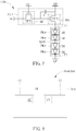
FIG. 1 depicts a schematic circuit diagram of an electronic device according to a first embodiment of the present disclosure; -
FIG.2 schematically illustrates a top view of the light-emitting unit according to the first embodiment of the present disclosure; -
FIG. 3 schematically illustrates a cross-sectional view of the light-emitting unit ofFIG. 2 taken along a line A-A'; -
FIG. 4 depicts a schematic circuit diagram of an electronic device according to a second embodiment of the present disclosure; -
FIG. 5 depicts a schematic circuit diagram of an electronic device according to a third embodiment of the present disclosure; -
FIG. 6 schematically illustrates a top view of a single package according to the third embodiment of the present disclosure; -
FIG. 7 depicts a schematic circuit diagram of an electronic device according to a fourth embodiment of the present disclosure; -
FIG. 8 schematically illustrates a top view of a single package according to the fourth embodiment of the present disclosure; -
FIG. 9 depicts a schematic circuit diagram of an electronic device according to a fifth embodiment of the present disclosure; -
FIG. 10 depicts a schematic circuit diagram of an electronic device according to a sixth embodiment of the present disclosure; -
FIG. 11 schematically illustrates an electronic device according to a seventh embodiment of the present disclosure; and -
FIG. 12 schematically illustrates an electronic device according to an eighth embodiment of the present disclosure. - The present disclosure may be understood by reference to the following detailed description, taken in conjunction with the drawings as described below. It is noted that, for purposes of illustrative clarity and being easily understood by the readers, certain elements in various drawings may not be drawn to scale. In addition, the number and dimension of each component shown in drawings are only illustrative and are not intended to limit the scope of the present disclosure.
- Certain terms are used throughout the description and following claims to refer to particular components. As one skilled in the art will understand, electronic equipment manufacturers may refer to a component by different names. This document does not intend to distinguish between components that differ in name but not function. In the following description and in the claims, the terms "include", "comprise" and "have" are used in an open-ended fashion, and thus should be interpreted to mean "include, but not limited to...". It will be understood that when a component is referred to as being "coupled" to another component (or its variant), it can be directly connected to the another component, or indirectly connected (e.g. electrically connected) to the another component through one or more components.
- It should be noted that the technical features in different embodiments described in the following can be replaced, recombined, or mixed with one another to constitute another embodiment without departing from the spirit of the present disclosure.
- In the present disclosure, the term "switch component" includes a transistor or other suitable switch components (e.g. IC). For example, the transistor may include a thin-film transistor, a metal oxide semiconductor (MOS) transistor, or other suitable transistors. In the following embodiments, a thin film transistor (e.g. the first thin-film transistor TFT1 and the second thin-film transistor TFT2) may be an illustrative example of the switch component, but the thin film transistor may be replaced by other switch components.
- Refer to
FIG. 1 which depicts a schematic circuit diagram of an electronic device (the electronic device is a light-emitting device in this embodiment and may be display device or light detecting device in other embodiments) according to a first embodiment of the present disclosure. As shown inFIG. 1 , the electronic device LD1 may include a light-emitting unit LU1 and at least one circuit unit CU1. The light-emitting unit LU1 may be referred to as a light-emitting diode chip or light-emitting diode unit with more complicate package. The light-emitting unit LU1 includes at least two diodes DC (diode die) coupled in series. Each diode DC has an anode and a cathode, in which the anode of one of the diodes DC is coupled to the cathode of another one of the diodes DC. The light-emitting unit LU1 may have a first end T1 and a second end T2. In this embodiment, the first end T1 is coupled to the anode of the serial diodes DC that is not coupled to the cathodes, and the second end T2 is coupled to the cathode of the serial diodes DC that is not coupled to the anodes. In other embodiments, the first end T1 is coupled to the cathode of the serial diodes that is not coupled to the anodes, and the second end T2 is coupled to the anode of the serial diodes that is not coupled to the cathodes. In this embodiment, the first end T1 of the light-emitting unit LU1 is coupled to a second end of the circuit unit CU1, and the second end T2 of the light-emitting unit LU1 is coupled to the low power source LP. Also, a first end of the circuit unit CU1 is coupled to a high power source HP. In other embodiment, the first end T1 of the light-emitting unit LU1 is coupled to the high power source HP, the second end T2 of the light-emitting unit LU1 is coupled to the first end of the circuit unit CU1, and a second end of the circuit unit CU1 is coupled to the low power source LP. - Additionally, at least one of the diodes DC is a light-emitting diode for generating light. In this embodiment, all of the diodes DC are the light-emitting diodes. In other embodiments, the diodes DC may be a combination of a light-emitting diode and a non-light-emitting diode with other function (e.g., sensor or rectifier). The light-emitting diode may be for example inorganic light-emitting diode or organic light-emitting diode. The diodes DC of the present disclosure coupled in series are not limited to be light-emitting diodes. In another embodiment, at least one of the diodes DC coupled in series may be another non-light-emitting diode. In another embodiment, the light-emitting unit LU1 may also include at least one diode coupled in parallel to one of the aforementioned diodes, or coupled in parallel to the aforementioned serial diodes DC, but the present disclosure is not limited thereto. The purpose of the present disclosure is mainly to increase the proportion of power of the light-emitting unit LU1, so any circuit design with the diodes DC coupled in series or in parallel that is capable of achieving this effect can be applied to the present disclosure.
- The circuit unit CU1 is coupled to the light-emitting unit LU1 and used for driving the light-emitting unit LU1 to generate light, in which an end (first end or second end) of the circuit unit CU1 is coupled to one of the first end T1 and the second end T2 of the light-emitting unit LU1 and a power source respectively. In this embodiment, the circuit unit CU1 may include a driving unit DU and a switch unit SU, in which the switch unit SU is used for controlling the switch of the driving unit DU. For example, in this embodiment, the driving unit DU may include at least one first thin-film transistor TFT1 disposed on substrate by photolithography process, and a source and a drain of the first thin-film transistor TFT1 are coupled to the first end T1 and a high power source HP respectively. The first thin-film transistor for example has an active layer, and a material of the active layer includes at least one of low temperature polysilicon semiconductor, amorphous semiconductor and metal oxide semiconductor. The high power source HP may be a DC voltage source with high voltage level, and the low power source LP may have a ground level or a common voltage level for example, but the present disclosure is not limited thereto. The switch unit SU may include at least one transistor. The transistor of the switch unit SU in this embodiment may include a second thin-film transistor TFT2 disposed on substrate by a photolithography process, in which a gate, a source and a drain of the second thin-film transistor TFT2 may be coupled to a switch signal source, a gate of the first thin-film transistor TFT1 and a data signal source. Further, the circuit unit CU1 may include a capacitor C coupled to a drain and the gate of the first thin-film transistor TFT1 respectively, and the capacitor C maintains the voltage between the drain and the gate of the first thin-film transistor TFT1 while the second thin-film transistor TFT2 is turned off. The electronic device LD1 serves as a sub-pixel of a display panel is taken as an example, in which in the thin-film transistor TFT2, the gate may be coupled to the switch signal source through a gate line GL, and the drain is coupled to the data signal source through a data line DL, but not limited thereto. In a variant embodiment, the source and the drain of the thin-film transistor may be exchanged. The operation and effect of the present disclosure is further detailed in the following description and compared to the traditional electronic device using a single light-emitting diode. It should be noted that the light-emitting diode is a current driving component, so the voltage drops, each of which is between two ends of each light-emitting diode, are designed to be substantially identical. For this reason, a voltage drop of single light-emitting diode is less than a voltage drop of each of the plurality of light-emitting diodes coupled in series. Also, when the power consumption of the single light-emitting diode and the power consumption of the light-emitting diodes coupled in series are identical, a size of the single light-emitting diode is required to be greater than a size of one of the plurality of light-emitting diodes, in which the driving current of the single light-emitting diode is greater than the driving current of the plurality of the light-emitting diodes. Since the voltage drop of the plurality of the light-emitting diodes coupled in series is greater than that of the single light-emitting diode, a proportion of the power consumption of the plurality of light-emitting diodes coupled in series to the total power consumption of the electronic device LD1 with the plurality of light-emitting diodes is higher than a proportion of the power consumption of the single light-emitting diode to the power consumption of the electronic device with single light-emitting diode; i.e., a power consumption of the light-emitting unit LU1 utilizing a plurality of light-emitting diodes with smaller size coupled in series to generate light has higher proportion in whole electronic device LD1 compared to the light-emitting unit utilizing single light-emitting diode with larger size to generate light. Thus, the proportion of the power consumption of the electronic device LD1 used in the light-emitting unit LU1 can be increased. Accordingly, the proportion of power of at least two light-emitting diodes coupled in series with smaller size in the electronic device LD1 of this embodiment can be greater than the proportion of power of the single light-emitting diode with larger size in the traditional electronic device. Besides, since the driving current of the light-emitting diodes coupled in series is lower than the driving current of the single light-emitting diode, which means the turn-on current of the first thin-film transistor TFT 1 (or switch component) for driving the light-emitting unit LU1 is lower than the turn-on current of the traditional thin-film transistor (or switch component) for driving the single light-emitting diode, the load of the first thin-film transistor TFT1 (or switch component) of this embodiment can be lower than the load of the traditional thin-film transistor (or switch component). In other words, the design of the light-emitting unit LU1 of this embodiment can prolong the lifetime of the first thin-film transistor TFT1 (or switch component). For example, the voltage drop of the light-emitting diode is 2V. When the driving current of the light-emitting diode of the traditional electronic device is 20mA, the power of the light-emitting unit of the traditional electronic device is 40mW. When the voltage drop between the drain and the source of the thin-film transistor (or switch component) for driving is 8V, the voltage drop between the high power source and the lower power source is 10V, and therefore, the proportion of the power consumption of the light-emitting unit of the traditional electronic device (2×20mW) to the power consumption of the traditional electronic device (10×20mW) is 1/5. However, when the driving current of each of the light-emitting diodes in this embodiment is reduced to be 5mA, and the voltage drop of two ends of each light-emitting diode is 2V, the light-emitting unit LU1 of this embodiment requires four light-emitting diodes coupled in series to have the voltage drop of 8V in the same power consumption situation as the traditional total power consumption (that is 40mW). In the situation that the voltage drop between the drain and the source of the first thin-film transistor TFT1 (or switch component) is also 8V, the voltage drop between the high power source HP and the low power source LP is 16V, so a proportion of the power consumption of the light-emitting unit LU1 (5 × 8mW) to the power consumption of the electronic device LD1 (5 × 16mW) can be increased to be 1/2. Additionally, since the driving current for driving the light-emitting diodes is reduced to be 5mA in this embodiment, the voltage drop between the drain and the source of the first thin-film transistor TFT1 (or switch component) may be reduced to be 4V. Accordingly, the voltage drop between the high power source HP and the low power source LP is 12V. Although the voltage drop between the high power source HP and the low power source LP requires to be increased, the proportion of the power consumption of the light-emitting unit LU1 (5×8mW) to the power consumption of the electronic device LD1 (5×12mW) can be significantly increased to be 3/4. Furthermore, since the driving current falls to be 5mA, the turn-on current of the first thin-film transistor TFT1 can also be lowered, and accordingly, the load of the first thin-film transistor TFT1 (or switch component) for driving the light-emitting diodes is mitigated. For this reason, heat generated from the operation of the first thin-film transistor TFT1 (or switch component) can be lowered to rise the lifetime of the first thin-film transistor TFT1. In other words, through coupling a plurality of light-emitting diodes with smaller size in series, not only the electronic device LD1 of this embodiment can have higher power conversion efficiency and higher proportion of power, but also the lifetime of the first thin-film transistor TFT1 (or switch component) in the driving unit SU for driving the light-emitting unit LU1 can be effectively improved. When the electronic device LD1 serves as a pixel or a sub-pixel of the display panel, the driving unit DU of the present disclosure is not limited to be composed of a single first thin-film transistor TFT1 (or switch component) and may include a plurality of thin-film transistors (or a plurality of switch components), and hence, the design of coupling the light-emitting diodes with smaller size in series can not only lower the load of the single thin-film transistor (or switch component) but also lower the loads of the thin-film transistors (or switch components). In another embodiment, the circuit unit CU1 may further include three thin-film transistors or four thin-film transistors (or switch components). In this embodiment, the electronic device LD1 may be used for displaying image alone, and the light-emitting unit LU1 of which may be pixel or sub-pixel for displaying images directly. In another embodiment, the electronic device LD1 may be used as a backlight source of the display panel.
- Refer to
FIG. 2 and FIG. 3 , in whichFIG.2 schematically illustrates a top view of the light-emitting unit according to the first embodiment of the present disclosure, andFIG. 3 schematically illustrates a cross-sectional view of the light-emitting unit ofFIG. 2 taken along a line A-A'. As shown inFIG. 2 and FIG. 3 , the light-emitting unit LU1 of this embodiment includes a package PK1, and the diodes DC are disposed in (enclosed within) the package PK1. In this embodiment, since each diode DC is the light-emitting diode, each diode DC may, for example but not limited to, include an n-type semiconductor layer SC2, a light-emitting layer LL disposed on the n-type semiconductor layer SC2 and a p-type semiconductor layer SC1 disposed on the light-emitting layer LL. Each diode DC may have an anode AE and a cathode CE. The package PK1 may further include a base substrate Sub, connecting lines CL and insulation layer IN. For example, the light-emitting unit LU1 includes four diodes DC, in which the diodes DC are arranged in an array formation on the base substrate Sub and be separated from each other, parts of the connecting lines CL are coupled to the anodes and the cathodes of the didoes DC adjacent to each other to serially couple to the diodes DC in the same package PK1, and the connecting lines CL coupled to two ends of the serial diodes can be regarded as the first end T1 and the second end T2 of the light-emitting unit LU1 or may be coupled to the outer conductive pins that form the first end T1 and the second end T2 of the light-emitting unit LU1. The insulation layer IN may be disposed to the connecting lines CL and the diodes DC respectively. The material of base substrate Sub may be glass, glass fiber, plastic, silicon wafer, or aluminum oxide. - It is noted that since the refractive index of the material for fabricating the light-emitting diode, such as 2.5, is greater than the refractive index outside, the p-type semiconductor layer SC1 and the n-type semiconductor layer SC2 easily form an optical waveguide structure, which reduces light leaking out from the top surface of the n-type semiconductor layer SC2 and causes light to easily emit out from the edge of the light-emitting layer LL. Thus, when the total exposed edge length of the light-emitting diode is longer, the amount of emitted light is greater. In this embodiment, because the light-emitting diodes DC in the light-emitting unit LU1 have smaller size, the light-emitting diodes DC have longer total edge length than the single light-emitting diode with larger size. Thus, under the same power consumption, the light-emitting unit LU1 of this embodiment has a higher amount of emitted light so as to generate light with higher brightness. For example, a length of an edge of the traditional rectangular light-emitting diode is 100µm, the power consumption of which per unit area is (2×20)/(100×100)=1/250mW/µm2, and a total edge length of which is 400µm. Under the same power consumption per unit area, a length of an edge of each light-emitting diode should be 50µm, and the total edge length should be (4×50)×4=800µm, so that the light-emitting unit LU1 of this embodiment can generate greater brightness than that of the traditional light-emitting unit.
- The electronic device of the present disclosure is not limited to the aforementioned embodiment, and may have other different variant embodiments or embodiments. To simplify the description and make it easier to compare the difference between the first embodiment and other embodiments, the identical components in each of the following embodiments are marked with identical symbols as the first embodiment, and the following description will detail the dissimilarities among different embodiments and the identical features will not be redundantly described.
- Refer to
FIG. 4 , which depicts a schematic circuit diagram of an electronic device according to a second embodiment of the present disclosure. As shown inFIG. 4 , in the light-emitting unit LU2 of the electronic device LD2 provided by this embodiment, the first end T1 (anode) is coupled to the high power source HP, and the second end T2 is coupled to an end of the circuit unit CU2 as compared with the first embodiment. Also, another end of the circuit unit CU2 is coupled to the low power source LP. Specifically, the drain and the source of the first thin-film transistor TFT1 (or the switch component) of the circuit unit CU2 are coupled to the second end T2 of the light-emitting unit LU2 and the low power source LP respectively. Further, the capacitor C is coupled to the gate and the source of the first thin-film transistor TFT1 (or the switch component) respectively. - Refer to
FIG. 5 andFIG. 6 , in whichFIG. 5 depicts a schematic circuit diagram of an electronic device according to a third embodiment of the present disclosure, andFIG. 6 schematically illustrates a top view of a single package according to the third embodiment of the present disclosure. As shown inFIG. 5 andFIG. 6 , the diodes DC of the electronic device LD3 provided by this embodiment may be disposed in (enclosed within) at least two packages PK3 respectively as compared with the first embodiment. In this embodiment, the light-emitting unit LU3 may include at least four diodes DC, and the light-emitting unit LU3 may include at least two packages PK3, in which at least two of the diodes DC are disposed in (enclosed within) one of the packages PK3, and at least another two of the diodes DC are disposed in (enclosed within) another one of the packages PK3. For example, each package PK3 includes a base substrate Sub and connecting lines CL, and the connecting lines CL are used for coupling the light-emitting diodes DC in series. Also, the packages PK3 may be serially coupled after being disposed on an array substrate of display panel or circuit board of backlight module. In another embodiment, the light-emitting unit LU3 and the circuit unit CU1 of the electronic device LD3 may adopt the connection method of the above second embodiment. - Refer to
FIG. 7 and FIG. 8 , in whichFIG. 7 depicts a schematic circuit diagram of an electronic device according to a fourth embodiment of the present disclosure,FIG. 8 schematically illustrates a top view of a single package according to the fourth embodiment of the present disclosure. As shown inFIG. 7 and FIG. 8 , each of the diodes DC of the electronic device LD4 provided by this embodiment may be disposed in (enclosed within) one corresponding package PK4 as compared with the first embodiment. The light-emitting unit LU4 includes four diodes DC is taken as an example, in which the light-emitting unit LU4 includes four packages PK4, each of which includes a base substrate Sub and connecting lines CL, and the connecting lines CL are coupled to the anodes AE and the cathodes CE of the light-emitting diodes DC respectively. Also, the packages PK4 may be serially coupled after being disposed on array substrate of display panel or circuit board of backlight module. In another embodiment, the light-emitting unit LU4 and the circuit unit CU1 of the electronic device LD4 may adopt the connection method of the above second embodiment. - Refer to
FIG. 9 , which depicts a schematic circuit diagram of an electronic device according to a fifth embodiment of the present disclosure. As shown inFIG. 9 , in this embodiment, the electronic device LD5 includes a plurality of circuit units CU5 coupled in parallel, and the circuit units CU5 are coupled to an end of the light-emitting unit LU1, as compared with the first embodiment. In this embodiment, each circuit unit CU5 is coupled to the first end T1 (anode) of the light-emitting unit LU1 and the high power source HP respectively, and each circuit unit CU5 may, for example, be the same as the circuit unit of the first embodiment, but not limited thereto. It is noted that the turn-on current of the thin-film transistor (or switch component) for driving the light-emitting diodes is the driving current of each light-emitting diode, and the thin-film transistor (or the switch component) is operated in the saturation region, so when the driving current for driving the light-emitting diodes is be greater than the turn-on current of the first thin-film transistor TFT1 (or switch component) of single circuit unit CU5, the driving current for driving the light-emitting diodes can be increased by coupling a plurality of circuit units CU5 in parallel in this embodiment. For example, since the brightness of the backlight source is greater than a brightness of single pixel or single sub-pixel, the light-emitting diodes in the light-emitting unit LU1 require higher driving current. Through coupling the circuit units CU5 in parallel, the light-emitting diodes can generate light with required brightness. For example, the number of the circuit units CU5 may be substantially 100 to 200, but not limited thereto, and the number of the circuit units CU5 may be mainly determined by the driving current of the light-emitting unit LU1. It is noted that since the light-emitting unit LU1 of this embodiment includes a plurality of diodes DC coupled in series, under condition of the same power consumption per unit area, the driving circuit of the diode DC can be reduced, thereby lowering the number of the circuit units CU5 of the light-emitting unit LU1. In another embodiment, the light-emitting unit LU1 and the circuit units CU5 of the electronic device LD5 may adopt the connection method of the above second embodiment; that is to say, each circuit unit CU5 may be coupled to the second end T2 (cathode) of the light-emitting unit LU1 and the low power source LP respectively. - Refer to
FIG. 10 , which depicts a schematic circuit diagram of an electronic device according to a sixth embodiment of the present disclosure. As shown inFIG. 10 , the circuit unit CU6 of the electronic device LD6 provided by this embodiment may further include at least one light-emitting control unit as compared with the first embodiment. In this embodiment, the circuit unit CU6 may include a data program storage unit DSU which includes a switch unit SU and a capacitor C. The circuit unit CU6 may include two light-emitting control units EU, one of them is coupled between the high power source HP and the first thin-film transistor TFT1 (or the switch component) of the driving unit DU, the other one of them is coupled between the light-emitting unit LU1 and the first thin-film transistor TFT1 (or the switch component) of the driving unit DU, and the light-emitting control units EU can be used for helping light-emitting unit LU1 to generate more stable light. Each light-emitting control unit EU may include a thin-film transistor or switch component. - The electronic device of the present disclosure may be further applied to a display device. Refer to
FIG. 11 , which schematically illustrates an electronic device according to a seventh embodiment of the present disclosure. As shown inFIG. 11 , the electronic device DA1 of this embodiment may include a light-emitting module LM including a plurality of light-emitting units LU and a display panel DP, and the light-emitting module LM is disposed on a back surface of the display panel DP, so that the display panel DP is disposed opposite to the light-emitting units LU. The display panel DP may be non-self-luminous display panel, so the light-emitting units LU are regarded as backlight source of the display panel DP, and light generated from the light-emitting module LM can enter the display panel DP from the back surface. The light-emitting units LU of this embodiment may adopt the electronic device of any one of the aforementioned embodiments. - Refer to
FIG. 12 , which schematically illustrates an electronic device according to an eighth embodiment of the present disclosure. As shown inFIG. 12 , the electronic device DA2 of this embodiment may include a plurality of light-emitting units LU, in which the electronic device DA2 may be a display panel, and each light-emitting unit LU may serve as a pixel or a sub-pixel of the electronic device DA2. The light-emitting units LU of this embodiment may adopt the electronic device of any one of the aforementioned embodiments. - As the mentioned above, because of the design of the light-emitting diodes with smaller size that are coupled in series, the electronic device of the present disclosure can have higher power conversion efficiency and higher proportion of power, and the lifetime of the thin-film transistor or the switch component in the driving unit can be effectively increased. Besides, since the used light-emitting diodes have smaller size, the light-emitting unit can generate light with higher brightness.
Claims (15)
- An electronic device (DA1, DA2, LD1, LD2, LD3, LD4, LD5, LD6), characterized by:a light-emitting unit (LU, LU1, LU2, LU3, LU4) having a first end (T1, T2), the light-emitting unit (LU, LU1, LU2, LU3, LU4) comprising a first diode (DC) and a second diode (DC) coupled in series, wherein at least one of the first diode (DC) and the second diode (DC) is a light-emitting diode; anda first circuit unit (CU1, CU2, CU5, CU6) comprising a first thin-film transistor (TFT1) coupled to the first end (T1, T2) of the light-emitting unit (LU, LU1, LU2, LU3, LU4) and a power source (HP, LP).
- The electronic device (DA1, DA2, LD1, LD2, LD3, LD4, LD5, LD6) according to claim 1, characterized in that the first thin-film transistor (TFT1) comprises an active layer, a material of the active layer comprises one of low-temperature polysilicon semiconductor, amorphous semiconductor and metal oxide semiconductor.
- The electronic device (LD5) according to any one of claims 1 to 2, characterized in that the electronic device (LD5) further comprises a second circuit unit (CU5), the first circuit unit (CU5) and the second circuit unit (CU5) are coupled in parallel, and the second circuit unit (CU5) is coupled to the first end (T1) of the light-emitting unit (LU1) and the power source (HP).
- The electronic device (DA1, DA2, LD1, LD2, LD3, LD4, LD5, LD6) according to any one of claims 1 to 3, characterized in that the first diode (DC) and the second diode (DC) are light-emitting diodes.
- The electronic device (DA1, DA2, LD1, LD2, LD3, LD5, LD6) according to any one of claims 1 to 4, characterized in that the first diode (DC) and the second diode (DC) are disposed in a first package (PK1, PK3).
- The electronic device (DA1, DA2, LD1, LD2, LD3, LD5, LD6) according to claim 5, characterized in that the first package (PK1, PK3) comprises a first base substrate (Sub), and the first diode (DC) and the second diode (DC) are disposed on the first base substrate (Sub).
- The electronic device (LD3, LD4) according to any one of claims 1 to 4, characterized in that the first diode (DC) is disposed in a first package (PK3, PK4), and the second diode (DC) is disposed in a second package (PK3, PK4).
- The electronic device (LD3) according to any one of claims 1 to 4, characterized in that the light-emitting unit (LU3) further comprises a third diode (DC), the first diode (DC), the second diode (DC) and the third diode (DC) are coupled in series, the first diode (DC) and the second diode (DC) are disposed in a first package (PK3), and the third diode is disposed in a second package (PK3).
- The electronic device (DA1, DA2, LD1, LD3, LD4, LD5, LD6) according to any one of claims 1 to 8, characterized in that the light-emitting unit (LU, LU1, LU3, LU4) further comprises a second end (T2) coupled to a low power source (LP), and the power source (HP) is a high power source (HP).
- The electronic device (DA1, DA2, LD1, LD3, LD4, LD5, LD6) according to any one of claims 1 to 9, characterized in that the first circuit unit (CU1, CU5) further comprises a capacitor (C) coupled to a gate and a drain of the first thin-film transistor (TFT1).
- The electronic device (LD2) according to any one of claims 1 to 8, characterized in that the light-emitting unit (LU2) further comprises a second end (T1) coupled to a high power source (HP), the power source (LP) is a low power source (LP), and the first circuit unit (CU2) further comprises a capacitor (C) coupled to a gate and a source of the first thin-film transistor (TFT1).
- The electronic device (DA1, DA2, LD1, LD2, LD3, LD4, LD5, LD6) according to any one of claims 1 to 11, characterized in that the first circuit unit (CU1, CU2, CU5, CU6) further comprises a second thin-film transistor (TFT2), one of a source and a drain of the second thin-film transistor (TFT2) is coupled to a gate of the first thin-film transistor (TFT1).
- The electronic device (DA1, DA2, LD1, LD2, LD3, LD4, LD5, LD6) according to claim 12, characterized in that the other one of the source and the drain of the second thin-film transistor (TFT2) is coupled to a data line (DL), and a gate of the second thin-film transistor (TFT2) is coupled to a scan line (GL).
- The electronic device (LD6) according to any one of claims 1 to 13, characterized in that the first circuit unit (CU6) further comprises at least one light-emitting control unit (EU), the light-emitting control unit (EU) is coupled to the first thin-film transistor (TFT1) and the first end of the light-emitting unit (LU1) or coupled to the first thin-film transistor (TFT1) and the power source (HP).
- The electronic device (DA1) according to any one of claims 1 to 14, characterized in that the electronic device (DA1) further comprises a display panel (DP) disposed opposite to the light-emitting unit (LU).
Applications Claiming Priority (1)
| Application Number | Priority Date | Filing Date | Title |
|---|---|---|---|
| CN201711366392.3A CN109936890B (en) | 2017-12-18 | 2017-12-18 | Electronic device |
Publications (2)
| Publication Number | Publication Date |
|---|---|
| EP3499592A1 true EP3499592A1 (en) | 2019-06-19 |
| EP3499592B1 EP3499592B1 (en) | 2024-07-03 |
Family
ID=64426657
Family Applications (1)
| Application Number | Title | Priority Date | Filing Date |
|---|---|---|---|
| EP18207156.3A Active EP3499592B1 (en) | 2017-12-18 | 2018-11-20 | Electronic device |
Country Status (3)
| Country | Link |
|---|---|
| US (1) | US10827582B2 (en) |
| EP (1) | EP3499592B1 (en) |
| CN (1) | CN109936890B (en) |
Families Citing this family (4)
| Publication number | Priority date | Publication date | Assignee | Title |
|---|---|---|---|---|
| TWI882306B (en) * | 2017-12-25 | 2025-05-01 | 日商半導體能源研究所股份有限公司 | Display and electronic device including the display |
| EP4651686A3 (en) | 2020-01-28 | 2026-02-25 | OLEDWorks LLC | Stacked oled microdisplay with low-voltage silicon backplane |
| CN118135931A (en) * | 2022-12-02 | 2024-06-04 | 群创光电股份有限公司 | Electronic Devices |
| KR20250118907A (en) * | 2024-01-30 | 2025-08-07 | 삼성디스플레이 주식회사 | Display device |
Citations (3)
| Publication number | Priority date | Publication date | Assignee | Title |
|---|---|---|---|---|
| US20080246040A1 (en) * | 2002-08-29 | 2008-10-09 | Seoul Semiconductor Co., Ltd. | Light emitting device having light emitting elements |
| US20100277403A1 (en) * | 2007-03-07 | 2010-11-04 | Ching-Yan Chao | Pixel structure of organic electroluminescent display panel and method of making the same |
| US20110037054A1 (en) * | 2009-08-17 | 2011-02-17 | Chan-Long Shieh | Amoled with cascaded oled structures |
Family Cites Families (17)
| Publication number | Priority date | Publication date | Assignee | Title |
|---|---|---|---|---|
| KR101212210B1 (en) | 2005-12-26 | 2012-12-13 | 엘지디스플레이 주식회사 | Backlight and liquid crystal display having the same |
| KR101198374B1 (en) * | 2006-02-23 | 2012-11-07 | 삼성디스플레이 주식회사 | Light emitting diode substrate and manufacturing method thereof and liquid crystal display using the same |
| US7928936B2 (en) * | 2006-11-28 | 2011-04-19 | Global Oled Technology Llc | Active matrix display compensating method |
| US8674914B2 (en) * | 2008-08-07 | 2014-03-18 | Sharp Kabushiki Kaisha | Display device and method of driving the same |
| KR101040855B1 (en) * | 2009-01-29 | 2011-06-14 | 삼성모바일디스플레이주식회사 | An emission control line driver and an organic light emitting display device using the same |
| EP2249623A1 (en) | 2009-05-04 | 2010-11-10 | Osram Gesellschaft mit Beschränkter Haftung | A low-dropout (LDO) current regulator |
| CN101656043B (en) * | 2009-09-01 | 2011-05-04 | 友达光电股份有限公司 | Pixel circuit, active matrix organic light emitting diode display and driving method |
| TW201123957A (en) * | 2009-12-17 | 2011-07-01 | Au Optronics Corp | Light-emitting apparatus, pixel structure, contact structure and method for fabricting the same |
| CN102270626B (en) * | 2010-06-01 | 2013-12-25 | 展晶科技(深圳)有限公司 | Polycrystal-encapsulated light-emitting diode |
| US8605232B2 (en) * | 2011-01-18 | 2013-12-10 | Apple Inc. | Display backlight having light guide plate with light source holes and dual source packages |
| KR102060793B1 (en) * | 2013-04-18 | 2020-02-12 | 삼성디스플레이 주식회사 | Display apparatus |
| US9773443B2 (en) | 2013-06-06 | 2017-09-26 | Intel Corporation | Thin film transistor display backplane and pixel circuit therefor |
| CN203872406U (en) * | 2014-05-22 | 2014-10-08 | 成都中科唯实仪器有限责任公司 | Large-power LED drive circuit in parallel connection mode |
| TWM493130U (en) * | 2014-06-11 | 2015-01-01 | Innolux Corp | Display device |
| US10157572B2 (en) * | 2016-11-01 | 2018-12-18 | Innolux Corporation | Pixel driver circuitry for a display device |
| CN109991751B (en) * | 2017-12-29 | 2021-05-11 | 中强光电股份有限公司 | Light field display device and method |
| TWI679627B (en) * | 2018-06-28 | 2019-12-11 | 友達光電股份有限公司 | Display panel |
-
2017
- 2017-12-18 CN CN201711366392.3A patent/CN109936890B/en active Active
-
2018
- 2018-10-04 US US16/151,350 patent/US10827582B2/en active Active
- 2018-11-20 EP EP18207156.3A patent/EP3499592B1/en active Active
Patent Citations (3)
| Publication number | Priority date | Publication date | Assignee | Title |
|---|---|---|---|---|
| US20080246040A1 (en) * | 2002-08-29 | 2008-10-09 | Seoul Semiconductor Co., Ltd. | Light emitting device having light emitting elements |
| US20100277403A1 (en) * | 2007-03-07 | 2010-11-04 | Ching-Yan Chao | Pixel structure of organic electroluminescent display panel and method of making the same |
| US20110037054A1 (en) * | 2009-08-17 | 2011-02-17 | Chan-Long Shieh | Amoled with cascaded oled structures |
Also Published As
| Publication number | Publication date |
|---|---|
| EP3499592B1 (en) | 2024-07-03 |
| CN109936890A (en) | 2019-06-25 |
| CN109936890B (en) | 2022-03-15 |
| US10827582B2 (en) | 2020-11-03 |
| US20190191504A1 (en) | 2019-06-20 |
Similar Documents
| Publication | Publication Date | Title |
|---|---|---|
| US12175945B2 (en) | Smart pixel lighting and display microcontroller | |
| US10356858B2 (en) | MicroLED display panel | |
| US12142192B2 (en) | Display module and display device | |
| EP3499592B1 (en) | Electronic device | |
| US10529701B2 (en) | MicroLED display panel | |
| TWI711199B (en) | Microled display panel | |
| US20110157114A1 (en) | Electroluminescence device | |
| KR20210044430A (en) | Method for manufacturing display apparatus, interposer substrate and computer program stored in a recording medium | |
| US20250318334A1 (en) | Display device and method for manufacturing display device | |
| CN105225628A (en) | Display device, display module and pixel structure thereof | |
| US10362651B2 (en) | Micro lighting device | |
| CN110033709A (en) | Micro- LED display panel | |
| US20190326268A1 (en) | Electronic device | |
| US11963429B2 (en) | Display module and display apparatus | |
| US20230375879A1 (en) | Flat lighting device and display device using light-emitting diode | |
| US20260029302A1 (en) | Inspection apparatus and inspection method of light emitting element | |
| TWI852082B (en) | Electronic device |
Legal Events
| Date | Code | Title | Description |
|---|---|---|---|
| PUAI | Public reference made under article 153(3) epc to a published international application that has entered the european phase |
Free format text: ORIGINAL CODE: 0009012 |
|
| STAA | Information on the status of an ep patent application or granted ep patent |
Free format text: STATUS: THE APPLICATION HAS BEEN PUBLISHED |
|
| AK | Designated contracting states |
Kind code of ref document: A1 Designated state(s): AL AT BE BG CH CY CZ DE DK EE ES FI FR GB GR HR HU IE IS IT LI LT LU LV MC MK MT NL NO PL PT RO RS SE SI SK SM TR |
|
| AX | Request for extension of the european patent |
Extension state: BA ME |
|
| STAA | Information on the status of an ep patent application or granted ep patent |
Free format text: STATUS: REQUEST FOR EXAMINATION WAS MADE |
|
| 17P | Request for examination filed |
Effective date: 20191008 |
|
| RBV | Designated contracting states (corrected) |
Designated state(s): AL AT BE BG CH CY CZ DE DK EE ES FI FR GB GR HR HU IE IS IT LI LT LU LV MC MK MT NL NO PL PT RO RS SE SI SK SM TR |
|
| STAA | Information on the status of an ep patent application or granted ep patent |
Free format text: STATUS: EXAMINATION IS IN PROGRESS |
|
| 17Q | First examination report despatched |
Effective date: 20200406 |
|
| GRAP | Despatch of communication of intention to grant a patent |
Free format text: ORIGINAL CODE: EPIDOSNIGR1 |
|
| STAA | Information on the status of an ep patent application or granted ep patent |
Free format text: STATUS: GRANT OF PATENT IS INTENDED |
|
| INTG | Intention to grant announced |
Effective date: 20240124 |
|
| RAP3 | Party data changed (applicant data changed or rights of an application transferred) |
Owner name: INNOLUX CORPORATION |
|
| RIN1 | Information on inventor provided before grant (corrected) |
Inventor name: TSENG, MING-CHUN Inventor name: TING, CHIN-LUNG Inventor name: MAO, LI-WEI |
|
| GRAS | Grant fee paid |
Free format text: ORIGINAL CODE: EPIDOSNIGR3 |
|
| GRAA | (expected) grant |
Free format text: ORIGINAL CODE: 0009210 |
|
| STAA | Information on the status of an ep patent application or granted ep patent |
Free format text: STATUS: THE PATENT HAS BEEN GRANTED |
|
| AK | Designated contracting states |
Kind code of ref document: B1 Designated state(s): AL AT BE BG CH CY CZ DE DK EE ES FI FR GB GR HR HU IE IS IT LI LT LU LV MC MK MT NL NO PL PT RO RS SE SI SK SM TR |
|
| REG | Reference to a national code |
Ref country code: CH Ref legal event code: EP |
|
| REG | Reference to a national code |
Ref country code: DE Ref legal event code: R096 Ref document number: 602018071228 Country of ref document: DE |
|
| REG | Reference to a national code |
Ref country code: LT Ref legal event code: MG9D |
|
| REG | Reference to a national code |
Ref country code: NL Ref legal event code: MP Effective date: 20240703 |
|
| REG | Reference to a national code |
Ref country code: DE Ref legal event code: R079 Ref document number: 602018071228 Country of ref document: DE Free format text: PREVIOUS MAIN CLASS: H01L0033620000 Ipc: H10H0020857000 |
|
| PG25 | Lapsed in a contracting state [announced via postgrant information from national office to epo] |
Ref country code: PT Free format text: LAPSE BECAUSE OF FAILURE TO SUBMIT A TRANSLATION OF THE DESCRIPTION OR TO PAY THE FEE WITHIN THE PRESCRIBED TIME-LIMIT Effective date: 20241104 |
|
| REG | Reference to a national code |
Ref country code: AT Ref legal event code: MK05 Ref document number: 1700761 Country of ref document: AT Kind code of ref document: T Effective date: 20240703 |
|
| PG25 | Lapsed in a contracting state [announced via postgrant information from national office to epo] |
Ref country code: NL Free format text: LAPSE BECAUSE OF FAILURE TO SUBMIT A TRANSLATION OF THE DESCRIPTION OR TO PAY THE FEE WITHIN THE PRESCRIBED TIME-LIMIT Effective date: 20240703 |
|
| PG25 | Lapsed in a contracting state [announced via postgrant information from national office to epo] |
Ref country code: PT Free format text: LAPSE BECAUSE OF FAILURE TO SUBMIT A TRANSLATION OF THE DESCRIPTION OR TO PAY THE FEE WITHIN THE PRESCRIBED TIME-LIMIT Effective date: 20241104 Ref country code: NL Free format text: LAPSE BECAUSE OF FAILURE TO SUBMIT A TRANSLATION OF THE DESCRIPTION OR TO PAY THE FEE WITHIN THE PRESCRIBED TIME-LIMIT Effective date: 20240703 |
|
| PG25 | Lapsed in a contracting state [announced via postgrant information from national office to epo] |
Ref country code: NO Free format text: LAPSE BECAUSE OF FAILURE TO SUBMIT A TRANSLATION OF THE DESCRIPTION OR TO PAY THE FEE WITHIN THE PRESCRIBED TIME-LIMIT Effective date: 20241003 |
|
| PG25 | Lapsed in a contracting state [announced via postgrant information from national office to epo] |
Ref country code: GR Free format text: LAPSE BECAUSE OF FAILURE TO SUBMIT A TRANSLATION OF THE DESCRIPTION OR TO PAY THE FEE WITHIN THE PRESCRIBED TIME-LIMIT Effective date: 20241004 Ref country code: FI Free format text: LAPSE BECAUSE OF FAILURE TO SUBMIT A TRANSLATION OF THE DESCRIPTION OR TO PAY THE FEE WITHIN THE PRESCRIBED TIME-LIMIT Effective date: 20240703 Ref country code: PL Free format text: LAPSE BECAUSE OF FAILURE TO SUBMIT A TRANSLATION OF THE DESCRIPTION OR TO PAY THE FEE WITHIN THE PRESCRIBED TIME-LIMIT Effective date: 20240703 |
|
| PG25 | Lapsed in a contracting state [announced via postgrant information from national office to epo] |
Ref country code: BG Free format text: LAPSE BECAUSE OF FAILURE TO SUBMIT A TRANSLATION OF THE DESCRIPTION OR TO PAY THE FEE WITHIN THE PRESCRIBED TIME-LIMIT Effective date: 20240703 |
|
| PG25 | Lapsed in a contracting state [announced via postgrant information from national office to epo] |
Ref country code: LV Free format text: LAPSE BECAUSE OF FAILURE TO SUBMIT A TRANSLATION OF THE DESCRIPTION OR TO PAY THE FEE WITHIN THE PRESCRIBED TIME-LIMIT Effective date: 20240703 |
|
| PG25 | Lapsed in a contracting state [announced via postgrant information from national office to epo] |
Ref country code: AT Free format text: LAPSE BECAUSE OF FAILURE TO SUBMIT A TRANSLATION OF THE DESCRIPTION OR TO PAY THE FEE WITHIN THE PRESCRIBED TIME-LIMIT Effective date: 20240703 Ref country code: IS Free format text: LAPSE BECAUSE OF FAILURE TO SUBMIT A TRANSLATION OF THE DESCRIPTION OR TO PAY THE FEE WITHIN THE PRESCRIBED TIME-LIMIT Effective date: 20241103 |
|
| PG25 | Lapsed in a contracting state [announced via postgrant information from national office to epo] |
Ref country code: CZ Free format text: LAPSE BECAUSE OF FAILURE TO SUBMIT A TRANSLATION OF THE DESCRIPTION OR TO PAY THE FEE WITHIN THE PRESCRIBED TIME-LIMIT Effective date: 20240703 Ref country code: HR Free format text: LAPSE BECAUSE OF FAILURE TO SUBMIT A TRANSLATION OF THE DESCRIPTION OR TO PAY THE FEE WITHIN THE PRESCRIBED TIME-LIMIT Effective date: 20240703 |
|
| PG25 | Lapsed in a contracting state [announced via postgrant information from national office to epo] |
Ref country code: ES Free format text: LAPSE BECAUSE OF FAILURE TO SUBMIT A TRANSLATION OF THE DESCRIPTION OR TO PAY THE FEE WITHIN THE PRESCRIBED TIME-LIMIT Effective date: 20240703 Ref country code: RS Free format text: LAPSE BECAUSE OF FAILURE TO SUBMIT A TRANSLATION OF THE DESCRIPTION OR TO PAY THE FEE WITHIN THE PRESCRIBED TIME-LIMIT Effective date: 20241003 |
|
| PG25 | Lapsed in a contracting state [announced via postgrant information from national office to epo] |
Ref country code: RS Free format text: LAPSE BECAUSE OF FAILURE TO SUBMIT A TRANSLATION OF THE DESCRIPTION OR TO PAY THE FEE WITHIN THE PRESCRIBED TIME-LIMIT Effective date: 20241003 Ref country code: PL Free format text: LAPSE BECAUSE OF FAILURE TO SUBMIT A TRANSLATION OF THE DESCRIPTION OR TO PAY THE FEE WITHIN THE PRESCRIBED TIME-LIMIT Effective date: 20240703 Ref country code: NO Free format text: LAPSE BECAUSE OF FAILURE TO SUBMIT A TRANSLATION OF THE DESCRIPTION OR TO PAY THE FEE WITHIN THE PRESCRIBED TIME-LIMIT Effective date: 20241003 Ref country code: LV Free format text: LAPSE BECAUSE OF FAILURE TO SUBMIT A TRANSLATION OF THE DESCRIPTION OR TO PAY THE FEE WITHIN THE PRESCRIBED TIME-LIMIT Effective date: 20240703 Ref country code: IS Free format text: LAPSE BECAUSE OF FAILURE TO SUBMIT A TRANSLATION OF THE DESCRIPTION OR TO PAY THE FEE WITHIN THE PRESCRIBED TIME-LIMIT Effective date: 20241103 Ref country code: HR Free format text: LAPSE BECAUSE OF FAILURE TO SUBMIT A TRANSLATION OF THE DESCRIPTION OR TO PAY THE FEE WITHIN THE PRESCRIBED TIME-LIMIT Effective date: 20240703 Ref country code: GR Free format text: LAPSE BECAUSE OF FAILURE TO SUBMIT A TRANSLATION OF THE DESCRIPTION OR TO PAY THE FEE WITHIN THE PRESCRIBED TIME-LIMIT Effective date: 20241004 Ref country code: FI Free format text: LAPSE BECAUSE OF FAILURE TO SUBMIT A TRANSLATION OF THE DESCRIPTION OR TO PAY THE FEE WITHIN THE PRESCRIBED TIME-LIMIT Effective date: 20240703 Ref country code: ES Free format text: LAPSE BECAUSE OF FAILURE TO SUBMIT A TRANSLATION OF THE DESCRIPTION OR TO PAY THE FEE WITHIN THE PRESCRIBED TIME-LIMIT Effective date: 20240703 Ref country code: CZ Free format text: LAPSE BECAUSE OF FAILURE TO SUBMIT A TRANSLATION OF THE DESCRIPTION OR TO PAY THE FEE WITHIN THE PRESCRIBED TIME-LIMIT Effective date: 20240703 Ref country code: BG Free format text: LAPSE BECAUSE OF FAILURE TO SUBMIT A TRANSLATION OF THE DESCRIPTION OR TO PAY THE FEE WITHIN THE PRESCRIBED TIME-LIMIT Effective date: 20240703 Ref country code: AT Free format text: LAPSE BECAUSE OF FAILURE TO SUBMIT A TRANSLATION OF THE DESCRIPTION OR TO PAY THE FEE WITHIN THE PRESCRIBED TIME-LIMIT Effective date: 20240703 |
|
| REG | Reference to a national code |
Ref country code: DE Ref legal event code: R097 Ref document number: 602018071228 Country of ref document: DE |
|
| PG25 | Lapsed in a contracting state [announced via postgrant information from national office to epo] |
Ref country code: RO Free format text: LAPSE BECAUSE OF FAILURE TO SUBMIT A TRANSLATION OF THE DESCRIPTION OR TO PAY THE FEE WITHIN THE PRESCRIBED TIME-LIMIT Effective date: 20240703 Ref country code: SM Free format text: LAPSE BECAUSE OF FAILURE TO SUBMIT A TRANSLATION OF THE DESCRIPTION OR TO PAY THE FEE WITHIN THE PRESCRIBED TIME-LIMIT Effective date: 20240703 Ref country code: DK Free format text: LAPSE BECAUSE OF FAILURE TO SUBMIT A TRANSLATION OF THE DESCRIPTION OR TO PAY THE FEE WITHIN THE PRESCRIBED TIME-LIMIT Effective date: 20240703 |
|
| PG25 | Lapsed in a contracting state [announced via postgrant information from national office to epo] |
Ref country code: EE Free format text: LAPSE BECAUSE OF FAILURE TO SUBMIT A TRANSLATION OF THE DESCRIPTION OR TO PAY THE FEE WITHIN THE PRESCRIBED TIME-LIMIT Effective date: 20240703 |
|
| PG25 | Lapsed in a contracting state [announced via postgrant information from national office to epo] |
Ref country code: IT Free format text: LAPSE BECAUSE OF FAILURE TO SUBMIT A TRANSLATION OF THE DESCRIPTION OR TO PAY THE FEE WITHIN THE PRESCRIBED TIME-LIMIT Effective date: 20240703 Ref country code: SK Free format text: LAPSE BECAUSE OF FAILURE TO SUBMIT A TRANSLATION OF THE DESCRIPTION OR TO PAY THE FEE WITHIN THE PRESCRIBED TIME-LIMIT Effective date: 20240703 |
|
| PLBE | No opposition filed within time limit |
Free format text: ORIGINAL CODE: 0009261 |
|
| STAA | Information on the status of an ep patent application or granted ep patent |
Free format text: STATUS: NO OPPOSITION FILED WITHIN TIME LIMIT |
|
| 26N | No opposition filed |
Effective date: 20250404 |
|
| REG | Reference to a national code |
Ref country code: CH Ref legal event code: PL |
|
| PG25 | Lapsed in a contracting state [announced via postgrant information from national office to epo] |
Ref country code: MC Free format text: LAPSE BECAUSE OF FAILURE TO SUBMIT A TRANSLATION OF THE DESCRIPTION OR TO PAY THE FEE WITHIN THE PRESCRIBED TIME-LIMIT Effective date: 20240703 |
|
| PG25 | Lapsed in a contracting state [announced via postgrant information from national office to epo] |
Ref country code: LU Free format text: LAPSE BECAUSE OF NON-PAYMENT OF DUE FEES Effective date: 20241120 |
|
| REG | Reference to a national code |
Ref country code: CH Ref legal event code: PL |
|
| PG25 | Lapsed in a contracting state [announced via postgrant information from national office to epo] |
Ref country code: CH Free format text: LAPSE BECAUSE OF NON-PAYMENT OF DUE FEES Effective date: 20241130 |
|
| REG | Reference to a national code |
Ref country code: BE Ref legal event code: MM Effective date: 20241130 |
|
| PG25 | Lapsed in a contracting state [announced via postgrant information from national office to epo] |
Ref country code: SE Free format text: LAPSE BECAUSE OF FAILURE TO SUBMIT A TRANSLATION OF THE DESCRIPTION OR TO PAY THE FEE WITHIN THE PRESCRIBED TIME-LIMIT Effective date: 20240703 |
|
| PG25 | Lapsed in a contracting state [announced via postgrant information from national office to epo] |
Ref country code: BE Free format text: LAPSE BECAUSE OF NON-PAYMENT OF DUE FEES Effective date: 20241130 |
|
| PG25 | Lapsed in a contracting state [announced via postgrant information from national office to epo] |
Ref country code: IE Free format text: LAPSE BECAUSE OF NON-PAYMENT OF DUE FEES Effective date: 20241120 |
|
| PGFP | Annual fee paid to national office [announced via postgrant information from national office to epo] |
Ref country code: DE Payment date: 20251022 Year of fee payment: 8 |
|
| PGFP | Annual fee paid to national office [announced via postgrant information from national office to epo] |
Ref country code: GB Payment date: 20251023 Year of fee payment: 8 |
|
| PGFP | Annual fee paid to national office [announced via postgrant information from national office to epo] |
Ref country code: FR Payment date: 20251023 Year of fee payment: 8 |
|
| PG25 | Lapsed in a contracting state [announced via postgrant information from national office to epo] |
Ref country code: HU Free format text: LAPSE BECAUSE OF FAILURE TO SUBMIT A TRANSLATION OF THE DESCRIPTION OR TO PAY THE FEE WITHIN THE PRESCRIBED TIME-LIMIT; INVALID AB INITIO Effective date: 20181120 |
|
| PG25 | Lapsed in a contracting state [announced via postgrant information from national office to epo] |
Ref country code: CY Free format text: LAPSE BECAUSE OF FAILURE TO SUBMIT A TRANSLATION OF THE DESCRIPTION OR TO PAY THE FEE WITHIN THE PRESCRIBED TIME-LIMIT; INVALID AB INITIO Effective date: 20181120 |