EP3499578A1 - Multi-view display device - Google Patents
Multi-view display device Download PDFInfo
- Publication number
- EP3499578A1 EP3499578A1 EP18211357.1A EP18211357A EP3499578A1 EP 3499578 A1 EP3499578 A1 EP 3499578A1 EP 18211357 A EP18211357 A EP 18211357A EP 3499578 A1 EP3499578 A1 EP 3499578A1
- Authority
- EP
- European Patent Office
- Prior art keywords
- subpixel
- green
- red
- blue
- view image
- Prior art date
- Legal status (The legal status is an assumption and is not a legal conclusion. Google has not performed a legal analysis and makes no representation as to the accuracy of the status listed.)
- Granted
Links
Images



Classifications
-
- G—PHYSICS
- G09—EDUCATION; CRYPTOGRAPHY; DISPLAY; ADVERTISING; SEALS
- G09G—ARRANGEMENTS OR CIRCUITS FOR CONTROL OF INDICATING DEVICES USING STATIC MEANS TO PRESENT VARIABLE INFORMATION
- G09G3/00—Control arrangements or circuits, of interest only in connection with visual indicators other than cathode-ray tubes
- G09G3/001—Control arrangements or circuits, of interest only in connection with visual indicators other than cathode-ray tubes using specific devices not provided for in groups G09G3/02 - G09G3/36, e.g. using an intermediate record carrier such as a film slide; Projection systems; Display of non-alphanumerical information, solely or in combination with alphanumerical information, e.g. digital display on projected diapositive as background
- G09G3/003—Control arrangements or circuits, of interest only in connection with visual indicators other than cathode-ray tubes using specific devices not provided for in groups G09G3/02 - G09G3/36, e.g. using an intermediate record carrier such as a film slide; Projection systems; Display of non-alphanumerical information, solely or in combination with alphanumerical information, e.g. digital display on projected diapositive as background to produce spatial visual effects
-
- H—ELECTRICITY
- H04—ELECTRIC COMMUNICATION TECHNIQUE
- H04N—PICTORIAL COMMUNICATION, e.g. TELEVISION
- H04N13/00—Stereoscopic video systems; Multi-view video systems; Details thereof
- H04N13/30—Image reproducers
- H04N13/349—Multi-view displays for displaying three or more geometrical viewpoints without viewer tracking
-
- H—ELECTRICITY
- H04—ELECTRIC COMMUNICATION TECHNIQUE
- H04N—PICTORIAL COMMUNICATION, e.g. TELEVISION
- H04N13/00—Stereoscopic video systems; Multi-view video systems; Details thereof
- H04N13/30—Image reproducers
-
- G—PHYSICS
- G09—EDUCATION; CRYPTOGRAPHY; DISPLAY; ADVERTISING; SEALS
- G09G—ARRANGEMENTS OR CIRCUITS FOR CONTROL OF INDICATING DEVICES USING STATIC MEANS TO PRESENT VARIABLE INFORMATION
- G09G3/00—Control arrangements or circuits, of interest only in connection with visual indicators other than cathode-ray tubes
- G09G3/20—Control arrangements or circuits, of interest only in connection with visual indicators other than cathode-ray tubes for presentation of an assembly of a number of characters, e.g. a page, by composing the assembly by combination of individual elements arranged in a matrix no fixed position being assigned to or needed to be assigned to the individual characters or partial characters
- G09G3/22—Control arrangements or circuits, of interest only in connection with visual indicators other than cathode-ray tubes for presentation of an assembly of a number of characters, e.g. a page, by composing the assembly by combination of individual elements arranged in a matrix no fixed position being assigned to or needed to be assigned to the individual characters or partial characters using controlled light sources
- G09G3/30—Control arrangements or circuits, of interest only in connection with visual indicators other than cathode-ray tubes for presentation of an assembly of a number of characters, e.g. a page, by composing the assembly by combination of individual elements arranged in a matrix no fixed position being assigned to or needed to be assigned to the individual characters or partial characters using controlled light sources using electroluminescent panels
- G09G3/32—Control arrangements or circuits, of interest only in connection with visual indicators other than cathode-ray tubes for presentation of an assembly of a number of characters, e.g. a page, by composing the assembly by combination of individual elements arranged in a matrix no fixed position being assigned to or needed to be assigned to the individual characters or partial characters using controlled light sources using electroluminescent panels semiconductive, e.g. using light-emitting diodes [LED]
- G09G3/3208—Control arrangements or circuits, of interest only in connection with visual indicators other than cathode-ray tubes for presentation of an assembly of a number of characters, e.g. a page, by composing the assembly by combination of individual elements arranged in a matrix no fixed position being assigned to or needed to be assigned to the individual characters or partial characters using controlled light sources using electroluminescent panels semiconductive, e.g. using light-emitting diodes [LED] organic, e.g. using organic light-emitting diodes [OLED]
- G09G3/3225—Control arrangements or circuits, of interest only in connection with visual indicators other than cathode-ray tubes for presentation of an assembly of a number of characters, e.g. a page, by composing the assembly by combination of individual elements arranged in a matrix no fixed position being assigned to or needed to be assigned to the individual characters or partial characters using controlled light sources using electroluminescent panels semiconductive, e.g. using light-emitting diodes [LED] organic, e.g. using organic light-emitting diodes [OLED] using an active matrix
-
- G—PHYSICS
- G09—EDUCATION; CRYPTOGRAPHY; DISPLAY; ADVERTISING; SEALS
- G09G—ARRANGEMENTS OR CIRCUITS FOR CONTROL OF INDICATING DEVICES USING STATIC MEANS TO PRESENT VARIABLE INFORMATION
- G09G5/00—Control arrangements or circuits for visual indicators common to cathode-ray tube indicators and other visual indicators
- G09G5/14—Display of multiple viewports
-
- H—ELECTRICITY
- H04—ELECTRIC COMMUNICATION TECHNIQUE
- H04N—PICTORIAL COMMUNICATION, e.g. TELEVISION
- H04N13/00—Stereoscopic video systems; Multi-view video systems; Details thereof
- H04N13/10—Processing, recording or transmission of stereoscopic or multi-view image signals
- H04N13/106—Processing image signals
- H04N13/133—Equalising the characteristics of different image components, e.g. their average brightness or colour balance
-
- H—ELECTRICITY
- H04—ELECTRIC COMMUNICATION TECHNIQUE
- H04N—PICTORIAL COMMUNICATION, e.g. TELEVISION
- H04N13/00—Stereoscopic video systems; Multi-view video systems; Details thereof
- H04N13/30—Image reproducers
- H04N13/302—Image reproducers for viewing without the aid of special glasses, i.e. using autostereoscopic displays
- H04N13/31—Image reproducers for viewing without the aid of special glasses, i.e. using autostereoscopic displays using parallax barriers
-
- H—ELECTRICITY
- H04—ELECTRIC COMMUNICATION TECHNIQUE
- H04N—PICTORIAL COMMUNICATION, e.g. TELEVISION
- H04N13/00—Stereoscopic video systems; Multi-view video systems; Details thereof
- H04N13/30—Image reproducers
- H04N13/349—Multi-view displays for displaying three or more geometrical viewpoints without viewer tracking
- H04N13/351—Multi-view displays for displaying three or more geometrical viewpoints without viewer tracking for displaying simultaneously
-
- H—ELECTRICITY
- H10—SEMICONDUCTOR DEVICES; ELECTRIC SOLID-STATE DEVICES NOT OTHERWISE PROVIDED FOR
- H10K—ORGANIC ELECTRIC SOLID-STATE DEVICES
- H10K50/00—Organic light-emitting devices
- H10K50/80—Constructional details
- H10K50/805—Electrodes
- H10K50/81—Anodes
- H10K50/818—Reflective anodes, e.g. ITO combined with thick metallic layers
-
- H—ELECTRICITY
- H10—SEMICONDUCTOR DEVICES; ELECTRIC SOLID-STATE DEVICES NOT OTHERWISE PROVIDED FOR
- H10K—ORGANIC ELECTRIC SOLID-STATE DEVICES
- H10K50/00—Organic light-emitting devices
- H10K50/80—Constructional details
- H10K50/805—Electrodes
- H10K50/82—Cathodes
-
- H—ELECTRICITY
- H10—SEMICONDUCTOR DEVICES; ELECTRIC SOLID-STATE DEVICES NOT OTHERWISE PROVIDED FOR
- H10K—ORGANIC ELECTRIC SOLID-STATE DEVICES
- H10K50/00—Organic light-emitting devices
- H10K50/80—Constructional details
- H10K50/84—Passivation; Containers; Encapsulations
- H10K50/844—Encapsulations
- H10K50/8445—Encapsulations multilayered coatings having a repetitive structure, e.g. having multiple organic-inorganic bilayers
-
- H—ELECTRICITY
- H10—SEMICONDUCTOR DEVICES; ELECTRIC SOLID-STATE DEVICES NOT OTHERWISE PROVIDED FOR
- H10K—ORGANIC ELECTRIC SOLID-STATE DEVICES
- H10K59/00—Integrated devices, or assemblies of multiple devices, comprising at least one organic light-emitting element covered by group H10K50/00
- H10K59/10—OLED displays
- H10K59/12—Active-matrix OLED [AMOLED] displays
- H10K59/121—Active-matrix OLED [AMOLED] displays characterised by the geometry or disposition of pixel elements
-
- H—ELECTRICITY
- H10—SEMICONDUCTOR DEVICES; ELECTRIC SOLID-STATE DEVICES NOT OTHERWISE PROVIDED FOR
- H10K—ORGANIC ELECTRIC SOLID-STATE DEVICES
- H10K59/00—Integrated devices, or assemblies of multiple devices, comprising at least one organic light-emitting element covered by group H10K50/00
- H10K59/10—OLED displays
- H10K59/12—Active-matrix OLED [AMOLED] displays
- H10K59/122—Pixel-defining structures or layers, e.g. banks
-
- H—ELECTRICITY
- H10—SEMICONDUCTOR DEVICES; ELECTRIC SOLID-STATE DEVICES NOT OTHERWISE PROVIDED FOR
- H10K—ORGANIC ELECTRIC SOLID-STATE DEVICES
- H10K59/00—Integrated devices, or assemblies of multiple devices, comprising at least one organic light-emitting element covered by group H10K50/00
- H10K59/10—OLED displays
- H10K59/17—Passive-matrix OLED displays
- H10K59/173—Passive-matrix OLED displays comprising banks or shadow masks
-
- H—ELECTRICITY
- H10—SEMICONDUCTOR DEVICES; ELECTRIC SOLID-STATE DEVICES NOT OTHERWISE PROVIDED FOR
- H10K—ORGANIC ELECTRIC SOLID-STATE DEVICES
- H10K59/00—Integrated devices, or assemblies of multiple devices, comprising at least one organic light-emitting element covered by group H10K50/00
- H10K59/30—Devices specially adapted for multicolour light emission
- H10K59/35—Devices specially adapted for multicolour light emission comprising red-green-blue [RGB] subpixels
- H10K59/353—Devices specially adapted for multicolour light emission comprising red-green-blue [RGB] subpixels characterised by the geometrical arrangement of the RGB subpixels
-
- H—ELECTRICITY
- H10—SEMICONDUCTOR DEVICES; ELECTRIC SOLID-STATE DEVICES NOT OTHERWISE PROVIDED FOR
- H10K—ORGANIC ELECTRIC SOLID-STATE DEVICES
- H10K59/00—Integrated devices, or assemblies of multiple devices, comprising at least one organic light-emitting element covered by group H10K50/00
- H10K59/30—Devices specially adapted for multicolour light emission
- H10K59/38—Devices specially adapted for multicolour light emission comprising colour filters or colour changing media [CCM]
-
- G—PHYSICS
- G09—EDUCATION; CRYPTOGRAPHY; DISPLAY; ADVERTISING; SEALS
- G09G—ARRANGEMENTS OR CIRCUITS FOR CONTROL OF INDICATING DEVICES USING STATIC MEANS TO PRESENT VARIABLE INFORMATION
- G09G2300/00—Aspects of the constitution of display devices
- G09G2300/04—Structural and physical details of display devices
- G09G2300/0439—Pixel structures
- G09G2300/0452—Details of colour pixel setup, e.g. pixel composed of a red, a blue and two green components
-
- G—PHYSICS
- G09—EDUCATION; CRYPTOGRAPHY; DISPLAY; ADVERTISING; SEALS
- G09G—ARRANGEMENTS OR CIRCUITS FOR CONTROL OF INDICATING DEVICES USING STATIC MEANS TO PRESENT VARIABLE INFORMATION
- G09G2320/00—Control of display operating conditions
- G09G2320/02—Improving the quality of display appearance
- G09G2320/028—Improving the quality of display appearance by changing the viewing angle properties, e.g. widening the viewing angle, adapting the viewing angle to the view direction
-
- G—PHYSICS
- G09—EDUCATION; CRYPTOGRAPHY; DISPLAY; ADVERTISING; SEALS
- G09G—ARRANGEMENTS OR CIRCUITS FOR CONTROL OF INDICATING DEVICES USING STATIC MEANS TO PRESENT VARIABLE INFORMATION
- G09G3/00—Control arrangements or circuits, of interest only in connection with visual indicators other than cathode-ray tubes
- G09G3/20—Control arrangements or circuits, of interest only in connection with visual indicators other than cathode-ray tubes for presentation of an assembly of a number of characters, e.g. a page, by composing the assembly by combination of individual elements arranged in a matrix no fixed position being assigned to or needed to be assigned to the individual characters or partial characters
- G09G3/22—Control arrangements or circuits, of interest only in connection with visual indicators other than cathode-ray tubes for presentation of an assembly of a number of characters, e.g. a page, by composing the assembly by combination of individual elements arranged in a matrix no fixed position being assigned to or needed to be assigned to the individual characters or partial characters using controlled light sources
- G09G3/30—Control arrangements or circuits, of interest only in connection with visual indicators other than cathode-ray tubes for presentation of an assembly of a number of characters, e.g. a page, by composing the assembly by combination of individual elements arranged in a matrix no fixed position being assigned to or needed to be assigned to the individual characters or partial characters using controlled light sources using electroluminescent panels
- G09G3/32—Control arrangements or circuits, of interest only in connection with visual indicators other than cathode-ray tubes for presentation of an assembly of a number of characters, e.g. a page, by composing the assembly by combination of individual elements arranged in a matrix no fixed position being assigned to or needed to be assigned to the individual characters or partial characters using controlled light sources using electroluminescent panels semiconductive, e.g. using light-emitting diodes [LED]
- G09G3/3208—Control arrangements or circuits, of interest only in connection with visual indicators other than cathode-ray tubes for presentation of an assembly of a number of characters, e.g. a page, by composing the assembly by combination of individual elements arranged in a matrix no fixed position being assigned to or needed to be assigned to the individual characters or partial characters using controlled light sources using electroluminescent panels semiconductive, e.g. using light-emitting diodes [LED] organic, e.g. using organic light-emitting diodes [OLED]
-
- H—ELECTRICITY
- H04—ELECTRIC COMMUNICATION TECHNIQUE
- H04N—PICTORIAL COMMUNICATION, e.g. TELEVISION
- H04N13/00—Stereoscopic video systems; Multi-view video systems; Details thereof
- H04N13/30—Image reproducers
- H04N2013/40—Privacy aspects, i.e. devices showing different images to different viewers, the images not being viewpoints of the same scene
-
- H—ELECTRICITY
- H04—ELECTRIC COMMUNICATION TECHNIQUE
- H04N—PICTORIAL COMMUNICATION, e.g. TELEVISION
- H04N2213/00—Details of stereoscopic systems
- H04N2213/001—Constructional or mechanical details
-
- H—ELECTRICITY
- H10—SEMICONDUCTOR DEVICES; ELECTRIC SOLID-STATE DEVICES NOT OTHERWISE PROVIDED FOR
- H10K—ORGANIC ELECTRIC SOLID-STATE DEVICES
- H10K71/00—Manufacture or treatment specially adapted for the organic devices covered by this subclass
Definitions
- the present invention relates to a multi-view display device, and more particularly, to a multi-view display device having a uniform high luminance.
- the flat display devices there are a liquid crystal display (LCD) device, a plasma display panel (PDP) device, a field emission display (FED) device, an electroluminescence display (ELD) device, an organic light emitting diode display (OLED) device, and the like.
- LCD liquid crystal display
- PDP plasma display panel
- FED field emission display
- ELD electroluminescence display
- OLED organic light emitting diode display
- the flat display devices exhibit excellent characteristics in terms of thinning, lightening, and reductions in the power consumption thereof and thus have rapidly replaced the conventional cathode ray tube (CRT) displays.
- CTR cathode ray tube
- the OLED device is a self-luminescent type device and does not require a backlight unit used in the LCD device as a non-self luminescent type device. As a result, the OLED device can be lightweight and thin.
- the OLED device has advantages of a viewing angle, a contrast ratio, and power consumption as compared with the LCD device. Furthermore, the OLED device may be driven with a low direct current (DC) voltage and has a rapid response speed. Moreover, since inner elements of the OLED device are in a solid state, the OLED device has high durability against an external impact and has a wide available temperature range.
- DC direct current
- the OLED device since a manufacturing process of the OLED device is simple, the OLED device has an advantage in that a production cost can be saved more than the conventional LCD.
- the OLED device is a self-luminescent element that emits light through an LED, and the LED emits light through an organic electroluminescence phenomenon.
- FIG. 1 is a band diagram of an LED having an emission principle based on a general organic electroluminescence phenomenon.
- an LED 10 is formed of an anode 21, a cathode 25, and an organic light emitting layer disposed therebetween.
- the organic light emitting layer is formed of a hole transport layer (HTL) 33, an electron transport layer (ETL) 35, and an emitting material layer (EML) 40 interposed between the HTL 33 and the ETL 35.
- HTL hole transport layer
- ETL electron transport layer
- EML emitting material layer
- HIL hole injection layer
- EIL electron injection layer
- the LED 10 when a positive voltage and a negative voltage are applied to the anode 21 and the cathode 25, respectively, the holes of the anode electrode 21 and the electrons of the cathode electrode 25 are transported to the EML 40 and form excitons, and when such excitons are transitioned from an excited state to a ground state, light is generated and emitted in the form of visible light by the EML 40.
- the OLED device including the LED 10 is designed as a two-dimensional display that can be simultaneously viewed by multiple users.
- Such the display characteristic of the display allows a viewer to view the same high-quality image from different angles.
- each user can view different information from the same display. For example, a driver in a vehicle may want to view navigation data while a passenger may want to watch a movie. In another example, each player in a computer game for two or more players may want to watch the game in his or her own view.
- the present invention is directed to a multi-view display device that substantially obviates one or more of the problems due to limitations and disadvantages of the related art.
- An object of the present invention is to provide a multi-view display device that can display two or more images such that the images are visible in different directions.
- Another object of the present invention is to provide a multi-view display device that can improve luminance of the multiple views.
- a multi-view display device includes: first to third subpixel groups which are on an array substrate and constitute a single unit pixel; first to third bank patterns corresponding to the first to third subpixel groups, respectively, and each including first and second inclined surfaces and a flat surface connecting the first and second inclined surfaces; and a red color filter corresponding to the first subpixel group, a green color filter disposed corresponding to the second subpixel group, and a blue color filter disposed corresponding to the third subpixel group, red, green and blue color filters being on a color filter encapsulation substrate facing the array substrate, wherein first red, green, and blue subpixels of the first subpixel group are on different surfaces of the first and second inclined surfaces and the flat surface of the first bank pattern, second red, green, and blue subpixels of the second subpixel group are on different surfaces of the first and second inclined surfaces and the flat surface of the second bank pattern, and third red, green, and blue subpixels
- the first to third red, green, and blue subpixels of the first to third subpixel groups are arranged such that a subpixel emitting one color light of red, green and blue lights is between two subpixels emitting the same color light that is different from the one color light.
- the first blue subpixel, the first red subpixel, and the first green subpixel are sequentially arranged in that order.
- the second red subpixel, the second green subpixel, and the second blue subpixel are sequentially arranged in that order.
- the third green subpixel, the third blue subpixel, and the third red subpixel are sequentially arranged in that order.
- an angle between the first and second inclined surfaces and a plane of the array substrate is in a range of 20 to 60°, which corresponds to a beam angle of light emitted from the first to third red, green, and blue subpixels.
- a subpixel on each of the first and second inclined surfaces emits a color light that is the same as a color light output from a color filter corresponding to one subpixel group of the first to third subpixel groups that is disposed adjacent to the subpixel on each of the first and second inclined surfaces emitting the color light.
- the first blue subpixel is disposed on the first inclined surface of the first bank pattern
- the first red subpixel is disposed on the flat surface of the first bank pattern
- the first green subpixel is disposed on the second inclined surface of the first bank pattern
- the second red subpixel is disposed on the first inclined surface of the second bank pattern
- the second green subpixel is disposed on the flat surface of the second bank pattern
- the second blue subpixel is disposed on the second inclined surface of the second bank pattern.
- the third green subpixel is disposed on the first inclined surface of the third bank pattern
- the third blue subpixel is disposed on the flat surface of the third bank pattern
- the third red subpixel is disposed on the second inclined surface of the third bank pattern.
- the first, second and third red subpixels each include a first electrode and a first organic light emitting layer disposed on each of the flat surface of the first bank pattern, the first inclined surface of the second bank pattern and the second inclined surface of the third bank pattern,
- the first, second and third green subpixels each include the first electrode and a second organic light emitting layer disposed on each of the second inclined surface of the first bank pattern, the flat surface of the second bank pattern and the first inclined surface of the third bank pattern,
- the first, second and third blue subpixels each include the first electrode and a third organic light emitting layer disposed on each of the first inclined surface of the first bank pattern, the second inclined surface of the second bank pattern and the flat surface of the third bank pattern.
- banks are between the first to third red, green, and blue subpixels such that the first electrode and the first to third organic light emitting layers have separated structures for each of the first to third red, green, and blue subpixels.
- a second electrode is on the first to third organic light emitting layers and the banks.
- the banks are between the first red, green and blue subpixels such that the first electrode and the first to third organic light emitting layers have separated structures for each of the first red, green, and blue subpixels.
- second electrode is disposed on the first to third organic light emitting layers including the banks.
- a red light emitted from the first red subpixel of the first subpixel group passes through the red color filter corresponding to the first subpixel group and displays the first-first view image.
- a green light emitted from the first green subpixel of the first subpixel group passes through the green color filter corresponding to the second subpixel group and displays the first-second view image.
- a red light emitted from the second red subpixel of the second subpixel group passes through the red color filter corresponding to the first subpixel group and displays the second-first view image.
- a green light emitted from the second green subpixel of the second subpixel group passes through the green color filter corresponding to the second subpixel group and displays the second-second view image.
- a blue light emitted from the second blue subpixel of the second subpixel group passes through the blue color filter corresponding to the third subpixel group and displays the second-third view image.
- a green light emitted from the third green subpixel of the third subpixel group passes through the green color filter corresponding to the second subpixel group and displays the third-second view image.
- a blue light emitted from the third blue subpixel of the third subpixel group passes through the blue color filter corresponding to the third subpixel group and displays the third-third view image.
- the color filter encapsulation substrate further includes a black matrix.
- the black matrix does not overlap with the first red subpixel, the second green subpixel, and the third blue subpixel.
- the black matrix overlaps by half with the first green and blue subpixels, the second red and blue subpixels, and the third green and red subpixels.
- first and second black matrices correspond to the first subpixel group.
- one end of the first black matrix corresponds to a central portion of the first blue subpixel, and the other end of the first black matrix corresponds to one end of the first red subpixel.
- the second black matrix is spaced apart from the first black matrix by a gap corresponding to a width of the first red subpixel.
- one end of the second black matrix corresponds to the other end of the first red subpixel, and the other end of the second black matrix corresponds to a central portion of the first green subpixel.
- the second black matrix is spaced apart from a third black matrix, which corresponds to the second subpixel group, by a gap corresponding to 1/2 of a width of the first green subpixel and 1/2 of a width of the second red subpixel.
- the gap between the first black matrix and the second black matrix satisfies (a cell gap + a thickness of black matrix) * tan(20°) * 2.
- the gap between the second black matrix and the third black matrix satisfies (a cell gap + a thickness of black matrix) * tan(60°).
- a gap between two subpixels respectively on the first and second inclined surfaces, which are respectively disposed in two neighboring bank patterns of the first to third bank patterns and are adjacent to each other, is less than a gap between a subpixel on the flat surface of each subpixel group and a subpixel on each of the first and second inclined surfaces of each subpixel group.
- the first to third bank patterns are on a passivation layer that is on a driving thin film transistor on the array substrate. In some embodiments.
- the driving thin film transistor is included in each of the first to third red, green, and blue subpixels, and includes a semiconductor layer, a gate insulating layer on the semiconductor layer, a gate electrode on the gate insulating layer, an interlayer insulating layer on the gate electrode, and source and drain electrodes on the interlayer insulating layer.
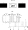
- FIG. 2A is a conceptual diagram schematically illustrating a multi-view display device with which images are visible in three different directions according to an embodiment of the present invention
- FIG. 2B is a schematic conceptual diagram for describing a privacy protection mode using a multi-view display device according to an embodiment of the present invention.
- the multi-view display device displays two or three different images on a single display panel 110 as a method of controlling a viewing angle.
- FIG. 2A a triple-view display device with which different images are visible when the display panel 110 is viewed from the center (V1), viewed from the left at an angle of 50° from the center (V3), and viewed from the right at an angle of 50° from the center (V2) is illustrated as an example.
- the multi-view display device simultaneously provides multiple images V1, V2, and V3, which differ from each other according to viewing directions, using the single display panel 110.
- Light incident from the display panel 110 is divided into the center, left, and right using barriers so that three different images V1, V2, and V3 are simultaneously displayed.
- the multi-view display device may be used to watch TV at the center and play game or surf the Internet at the left or right.
- the multi-view display device may also be applied as a vehicle navigation device and an advertisement display capable of multi-screen display.
- a vehicle navigation device while a navigation screen is provided to a driver and road information to a destination is displayed to the driver, a screen that allows tour information to be searched for may be displayed to a passenger of a front passenger seat, and a passenger of a back passenger seat may be allowed to watch a digital versatile disc (DVD) movie through a screen.
- DVD digital versatile disc
- the multi-view display device When the multi-view display device is applied in the advertisement display field, three different pieces of information may be displayed according to directions in which pedestrians walk. Since the multi-view display device is capable of showing different images V1, V2, and V3 to two or more users, the space and cost are significantly saved in comparison to when two or more separate display devices are used.
- a three-dimensional stereoscopic image may be realized when the multi-view display device is a dual-view display device configured to display two different images.
- the multi-view display device may realize a privacy protection mode as illustrated in FIG. 2B .
- a privacy protection mode a private image V1 is only provided to a user who views the display panel 110 from the center, and a user who views the display panel 110 from the left or right views black images or noise images V2 and V3.
- the private image V1 is an image that the user wants to keep invisible to others for security or privacy.
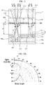
- FIG. 3 is a plan view schematically illustrating an arrangement of an array substrate and a color filter encapsulation substrate which constitute the multi-view display device according to an embodiment of the present invention.
- FIG. 3 for convenience of description, only a plurality of subpixels 1R-SP, 1G-SP, 1B-SP, 2R-SP, 2G-SP, 2B-SP, 3R-SP, 3G-SP, and 3B-SP and banks 119 configured to partition the subpixels 1R-SP, 1G-SP, 1B-SP, 2R-SP, 2G-SP, 2B-SP, 3R-SP, 3G-SP, and 3B-SP are illustrated, and only color filters R-CF, G-CF, and B-CF and black matrices BM are illustrated on a color filter encapsulation substrate 130.
- the multi-view display device may use an OLED device.
- the OLED device includes an array substrate 101 including a driving thin film transistor DTr (see FIG. 4 ) and an LED E (see FIG. 4 ), and the color filter encapsulation substrate 130 facing the array substrate 101.
- the plurality of subpixels 1R-SP, 1G-SP, 1B-SP, 2R-SP, 2G-SP, 2B-SP, 3R-SP, 3G-SP, and 3B-SP are arranged as matrices on the array substrate 101.
- the plurality of subpixels 1R-SP, 1G-SP, 1B-SP, 2R-SP, 2G-SP, 2B-SP, 3R-SP, 3G-SP, and 3B-SP are divided and defined into first to third subpixel groups 1GP, 2GP, and 3GP, and the first to third subpixel groups 1GP, 2GP, and 3GP constitute a single unit pixel P.
- the first to third subpixel groups 1GP, 2GP, and 3GP include first to third red subpixels 1R-SP, 2R-SP, and 3R-SP configured to emit red light, first to third green subpixels 1G-SP, 2G-SP, and 3G-SP configured to emit green light, and first to third blue subpixels 1B-SP, 2B-SP, and 3B-SP configured to emit blue light, respectively.
- the first subpixel group 1GP includes the first red subpixel 1R-SP, the first green subpixel 1G-SP, and the first blue subpixel 1B-SP.
- the second subpixel group 2GP includes the second red subpixel 2R-SP, the second green subpixel 2G-SP, and the second blue subpixel 2B-SP.
- the third subpixel group 3GP includes the third red subpixel 3R-SP, the third green subpixel 3G-SP, and the third blue subpixel 3B-SP.
- All of the first to third red subpixels 1R-SP, 2R-SP, and 3R-SP, the first to third green subpixels 1G-SP, 2G-SP, and 3G-SP, and the first to third blue subpixels 1B-SP, 2B-SP, and 3B-SP constitute a single unit pixel P.
- Each of the first to third red, green, and blue subpixels 1R-SP, 1G-SP, 1B-SP, 2R-SP, 2G-SP, 2B-SP, 3R-SP, 3G-SP, and 3B-SP includes an emissive region EA, and the bank 119 is disposed along an edge of each emissive region EA and forms a non-emissive region NEA ( Fig.3 ).
- the subpixels 1R-SP, 1G-SP, 1B-SP, 2R-SP, 2G-SP, 2B-SP, 3R-SP, 3G-SP, and 3B-SP are illustrated as being disposed in parallel at equal widths.
- the subpixels 1R-SP, 1G-SP, 1B-SP, 2R-SP, 2G-SP, 2B-SP, 3R-SP, 3G-SP, and 3B-SP may be disposed at different widths and have various other structures.
- a switching thin film transistor (not illustrated) and a driving thin film transistor DTr are disposed on the non-emissive region NEA of each of the subpixels 1R-SP, 1G-SP, 1B-SP, 2R-SP, 2G-SP, 2B-SP, 3R-SP, 3G-SP, and 3B-SP, and an LED E (see FIG. 4 ) which includes a first electrode 111 (see FIG. 4 ), an organic light emitting layer 113 (see FIG. 4 ), and a second electrode 115 (see FIG.
- the first to third subpixel groups 1GP, 2GP, and 3GP may display three view images V1, V2, and V3 using the first to third red, green, and blue subpixels 1R-SP, 1G-SP, 1B-SP, 2R-SP, 2G-SP, 2B-SP, 3R-SP, 3G-SP, and 3B-SP included in the subpixel groups 1GP, 2GP, and 3GP.
- the first subpixel group 1GP may display a first-first (i.e., 1-1) view image V1-1 using the first red subpixel 1R-SP, display a first-second (i.e., 1-2) view image V1-2 using the first green subpixel 1G-SP, and display a first-third (i.e., 1-3) view image V1-3 using the first blue subpixel 1B-SP.
- the second subpixel group 2GP and the third subpixel group 3GP may display a second-first (i.e., 2-1) view image V2-1 and a third-first (i.e., 3-1) view image V3-1 using the second red subpixel 2R-SP and the third red subpixel 3R-SP, respectively, display a second-second view image V2-2 (i.e., 2-2) and a third-second (i.e., 3-2) view image V3-2 using the second green subpixel 2G-SP and the third green subpixel 3G-SP, respectively, and display a second-third view image (i.e., 2-3) V2-3 and a third-third (i.e., 3-3) view image V3-3 using the second blue subpixel 2B-SP and the third blue subpixel 3B-SP, respectively,
- the first-first view image V1-1, the first-second view image V1-2, and the first-third view image V1-3 may display a single first view image V1.
- the second-first view image V2-1, the second-second view image V2-2, and the second-third view image V2-3 may display a single second view image V2.
- the third-first view image V3-1, the third-second view image V3-2, and the third-third view image V3-3 may display a single third view image V3.
- the single unit pixel P of this embodiment may display three view images of the first to third view images V1, V2, and V3 divided and defined into nine view images.
- the first blue subpixel 1B-SP, the first red subpixel 1R-SP, and the first green subpixel 1G-SP may be disposed in that order in a first direction of FIG. 3 .
- the first direction may be a longitudinal direction (i.e., length direction) of a gate line (not illustrated).
- the second red subpixel 2R-SP, the second green subpixel 2G-SP, and the second blue subpixel 2B-SP are disposed in that order.
- the third green subpixel 3G-SP, the third blue subpixel 3B-SP, and the third red subpixel 3R-SP are disposed in that order.
- a plurality of black matrices BM and a plurality of color filters R-CF, G-CF, and B-CF are disposed on the color filter encapsulation substrate 130.
- the black matrices BM and/or the color filters R-CF, G-CF, and B-CF may serve as barriers configured to spatially separate the nine view images.
- the red color filter R-CF may be disposed corresponding to the first subpixel group 1GP
- the green color filter G-CF may be disposed corresponding to the second subpixel group 2GP
- the blue color filter B-CF may be disposed corresponding to the third subpixel group 3GP.
- the first red, green, and blue subpixels 1R-SP, 1G-SP, and 1B-SP of the first subpixel group 1GP may be disposed to overlap with the red color filter R-CF
- the second red, green, and blue subpixels 2R-SP, 2G-SP, and 2B-SP of the second subpixel group 2GP may be disposed to overlap with the green color filter G-CF
- the third red, green, and blue subpixels 3R-SP, 3G-SP, and 3B-SP of the third subpixel group 3GP may be disposed to overlap with the blue color filter B-CF.
- red light emitted from the first red subpixel 1R-SP of the first subpixel group 1GP passes through the red color filter R-CF disposed at the color filter encapsulation substrate 130 and displays the first-first view image V1-1.
- green light and blue light emitted from the first green subpixel 1G-SP and the first blue subpixel 1B-SP of the first subpixel group 1GP are unable to pass through the red color filter R-CF which is disposed corresponding to the first subpixel group 1GP and, instead, respectively pass through the green color filter G-CF and the blue color filter B-CF, which are disposed corresponding to the second and third subpixel groups 2GP and 3GP disposed to neighbor the first subpixel group 1GP, and display the first-second view image V1-2 and the first-third view image V1-3.
- green light emitted from the second green subpixel 2G-SP of the second subpixel group 2GP passes through the green color filter G-CF disposed at the color filter encapsulation substrate 130 and displays the second-second view image V2-2.
- red light and blue light emitted from the second red subpixel 2R-SP and the second blue subpixel 2B-SP of the second subpixel group 2GP are unable to pass through the green color filter G-CF which is disposed corresponding to the second subpixel group 2GP and, instead, respectively pass through the red color filter R-CF and the blue color filter B-CF, which are disposed corresponding to the first and third subpixel groups 1GP and 3GP disposed to neighbor the second subpixel group 2GP, and display the second-first view image V2-1 and the second-third view image V2-3.
- blue light emitted from the third blue subpixel 3B-SP of the third subpixel group 3GP passes through the blue color filter B-CF disposed at the color filter encapsulation substrate 130 and displays the third-third view image V3-3.
- red light and green light emitted from the third red subpixel 3R-SP and the third green subpixel 3G-SP of the third subpixel group 3GP are unable to pass through the blue color filter B-CF which is disposed corresponding to the third subpixel group 3GP and, instead, respectively pass through the red color filter R-CF and the green color filter G-CF, which are disposed corresponding to the first and second subpixel groups 1GP and 2GP disposed to neighbor the third subpixel group 3GP, and display the third-first view image V3-1 and the third-third view image V3-3.
- the first-first view image V1-1 displayed through the red color filter R-CF, the first-second view image V1-2 displayed through the green color filter G-CF, and the first-third view image V1-3 displayed through the blue color filter B-CF realize the first view image V1.
- the second-first view image V2-1, the second-second view image V2-2, and the second-third view image V2-3 realize the second view image V2.
- the third-first view image V3-1, the third-second view image V3-2, and the third-third view image V3-3 realize the single third view image V3. Accordingly, the OLED device of this embodiment realizes the multi-view display device.
- the first-second view image V1-2, the first-third view image V1-3, the second-first view image V2-1, the second-third view image V2-3, the third-first view image V3-1, and the third-second view image V3-2 which are unable to pass through the color filters R-CF, G-CF, and B-CF disposed corresponding to the first to third subpixel groups 1GP, 2GP, and 3GP, respectively, and, instead, pass through other color filters R-CF, G-CF, and B-CF disposed corresponding to the neighboring subpixel groups 1GP, 2GP, and 3GP, are formed due to transmission of light emitted sideward from each of the subpixels 1R-SP, 1G-SP, 1B-SP, 2R-SP, 2G-SP, 2B-SP, 3R-SP, 3G-SP, and 3B-SP.
- the first-second view image V1-2, the first-third view image V1-3, the second-first view image V2-1, the second-third view image V2-3, the third-first view image V3-1, and the third-second view image V3-2 have a lower luminance in comparison to the first-first view image V1-1, the second-second view image V2-2, and the third-third view image V3-3 which pass through the color filters R-CF, G-CF, and B-CF disposed corresponding to the first to third subpixel groups 1GP, 2GP, and 3GP, respectively.
- the first-second view image V1-2, the first-third view image V1-3, the second-first view image V2-1, the second-third view image V2-3, the third-first view image V3-1, and the third-second view image V3-2 may be formed due to transmission of light emitted forward from each of the subpixels 1R-SP, 1G-SP, 1B-SP, 2R-SP, 2G-SP, 2B-SP, 3R-SP, 3G-SP, and 3B-SP. Accordingly, it is possible to realize uniform high luminance in all multi-view images.
- FIG. 4 is a cross-sectional view taken along line IV-IV of FIG. 3
- FIG. 5 is an enlarged view of portion A of FIG. 4 .
- FIGS. 6A to 6C are graphs of experimental results showing beam angles of light emitted from subpixels.
- the OLED device according to an embodiment of the present invention is classified into a top emission type and a bottom emission type according to a light transmission direction.
- a top emission type is classified into a top emission type and a bottom emission type according to a light transmission direction.
- an example in which the OLED device is a top emission type will be described.
- the OLED device includes an array substrate 101 on which a driving thin film transistor DTr and an LED E are formed, and a color filter encapsulation substrate 130 facing the array substrate 101.
- the array substrate 101 and the color filter encapsulation substrate 130 are adhered to each other, thereby forming the OLED device.
- a gate line (not illustrated), a data line (not illustrated), and a power line (not illustrated) are disposed on the array substrate 101 such that each of the subpixels 1R-SP, 1G-SP, 1B-SP, 2R-SP, 2G-SP, 2B-SP, 3R-SP, 3G-SP, and 3B-SP is defined.
- the plurality of subpixels 1R-SP, 1G-SP, 1B-SP, 2R-SP, 2G-SP, 2B-SP, 3R-SP, 3G-SP, and 3B-SP may be divided and defined into first to third subpixel groups 1GP, 2GP, and 3GP.
- the first to third subpixel groups 1GP, 2GP, and 3GP constitute a single unit pixel P.
- a semiconductor layer 103 is disposed on a switching region TrA of each of the subpixels 1R-SP, 1G-SP, 1B-SP, 2R-SP, 2G-SP, 2B-SP, 3R-SP, 3G-SP, and 3B-SP on the array substrate 101.
- the semiconductor layer 103 may be formed of silicon.
- the semiconductor layer 103 may include an active region 103a as a channel at a center portion thereof, and source and drain regions 103b and 103c doped with high-concentration impurities at both sides of the active region 103a.
- a gate insulating layer 105 is disposed on the semiconductor layer 103.
- a gate electrode 107 corresponding to the active region 103a of the semiconductor layer 103 and a gate line (not illustrated) which extends in one direction are disposed on the gate insulating layer 105.
- An interlayer insulating layer 109a is disposed on the gate electrode 107 and the gate line (not illustrated).
- first and second semiconductor layer contact holes 116 configured to respectively expose the source and drain regions 103b and 103c are disposed in the interlayer insulating layer 109a and the gate insulating layer 105.
- Source and drain electrodes 117a and 117b spaced apart from each other and configured to respectively be in contact with the source and drain regions 103b and 103c through the first and second semiconductor layer contact holes 116 are disposed on the interlayer insulating layer 109a.
- a passivation layer 109b having a drain contact hole 118 configured to expose the drain electrode 117b of the driving thin film transistor DTr is disposed on the source and drain electrodes 117a and 117b and the interlayer insulating layer 109a.
- the source and drain electrodes 117a and 117b, the semiconductor layer 103, the gate insulating layer 105, and the gate electrode 107 constitute the driving thin film transistor DTr.
- a switching thin film transistor is connected to the driving thin film transistor DTr.
- the switching thin film transistor may be formed of the same structure as the driving thin film transistor DTr.
- the driving thin film transistor DTr having a top gate structure with the semiconductor layer 103 formed as a polycrystalline silicon layer or oxide semiconductor layer is described by way of example.
- the driving thin film transistor DTr may have a bottom gate structure with the semiconductor layer 103 formed as an amorphous silicon layer.
- a light shielding layer (not illustrated) may be disposed below the semiconductor layer 103.
- a buffer layer (not illustrated) may be disposed between the light shielding layer and the semiconductor layer 103.
- the first to third bank patterns 200a, 200b, and 200c are disposed on the passivation layer 109b.
- the first to third bank patterns 200a, 200b, and 200c may be disposed to be spaced apart at predetermined gaps corresponding to the first to third subpixel groups 1GP, 2GP, and 3GP.
- Each of the first to third bank patterns 200a, 200b, and 200c may include first and second inclined surfaces 210 and 220 and a flat surface 230 configured to connect the first and second inclined surfaces 210 and 220.
- the first inclined surface 210 of the first bank pattern 200a may be disposed corresponding to the first blue subpixel 1B-SP of the first subpixel group 1GP
- the flat surface 230 of the first bank pattern 200a may be disposed corresponding to the first red subpixel 1R-SP of the first subpixel group 1GP
- the second inclined surface 220 of the first bank pattern 200a may be disposed corresponding to the first green subpixel 1G-SP of the first subpixel group 1GP.
- the first and second inclined surfaces 210 and 220 of the second bank pattern 200b may be disposed respectively corresponding to the second red subpixel 2R-SP and the second blue subpixel 2B-SP of the second subpixel group 2GP, and the flat surface 230 of the second bank pattern 200b may be disposed corresponding to the second green subpixel 2G-SP of the second subpixel group 2GP.
- the first and second inclined surfaces 210 and 220 of the third bank pattern 200c may be disposed respectively corresponding to the third green subpixel 3G-SP and the third red subpixel 3R-SP of the third subpixel group 3GP, and the flat surface 230 of the third bank pattern 200c may be disposed corresponding to the third blue subpixel 3B-SP of the third subpixel group 3GP.
- all of subpixels 1R-SP, 1G-SP, 1B-SP, 2R-SP, 2G-SP, 2B-SP, 3R-SP, 3G-SP, and 3B-SP of the first to third subpixel groups 1GP, 2GP, and 3GP may emit light forward and be able to realize uniform high luminance. This will be described in more detail below.
- First electrodes 111 each connected to the drain electrode 117b of the driving thin film transistor DTr and serving as an anode of the LED E with, for example, a material having a relatively high work function, may be disposed on the first to third bank patterns 200a, 200b, and 200c with the passivation layer 109b.
- the first electrode 111 may be formed of metal oxide such as indium tin oxide (ITO) or indium zinc oxide (IZO).
- ITO indium tin oxide
- IZO indium zinc oxide
- the first electrode 111 may be disposed for each of the subpixels 1R-SP, 1G-SP, 1B-SP, 2R-SP, 2G-SP, 2B-SP, 3R-SP, 3G-SP, and 3B-SP.
- the first electrode 111 of the first blue subpixel 1B-SP of the first subpixel group 1GP is disposed on the first inclined surface 210 of the first bank pattern 200a
- the first electrode 111 of the first red subpixel 1R-SP is disposed on the flat surface 230 of the first bank pattern 200a
- the first electrode 111 of the first green subpixel 1G-SP is disposed on the second inclined surface 220 of the first bank pattern 200a.
- the first electrode 111 of the second red subpixel 2R-SP of the second subpixel group 2GP is disposed on the first inclined surface 210 of the second bank pattern 200b
- the first electrode 111 of the second green subpixel 2G-SP is disposed on the flat surface 230 of the second bank pattern 200b
- the first electrode 111 of the second blue subpixel 2B-SP is disposed on the second inclined surface 220 of the second bank pattern 200b.
- the first electrode 111 of the third green subpixel 3G-SP of the third subpixel group 3GP is disposed on the first inclined surface 210 of the third bank pattern 200c
- the first electrode 111 of the third blue subpixel 3B-SP is disposed on the flat surface 230 of the third bank pattern 200c
- the first electrode 111 of the third red subpixel 3R-SP is disposed on the second inclined surface 220 of the third bank pattern 200c.
- Banks 119 are disposed between the first electrodes 111 disposed for each of the subpixels 1R-SP, 1G-SP, 1B-SP, 2R-SP, 2G-SP, 2B-SP, 3R-SP, 3G-SP, and 3B-SP.
- the first electrodes 111 may have separated structures for each of the subpixels 1R-SP, 1G-SP, 1B-SP, 2R-SP, 2G-SP, 2B-SP, 3R-SP, 3G-SP, and 3B-SP with the banks 119 as boundaries for each of the subpixels 1R-SP, 1G-SP, 1B-SP, 2R-SP, 2G-SP, 2B-SP, 3R-SP, 3G-SP, and 3B-SP.
- a width D2 ( Fig. 4 ) of the banks 119 which are disposed between the subpixels 1G-SP, 1B-SP, 2R-SP, 2B-SP, 3R-SP, and 3G-SP disposed on the first and second inclined surfaces 210 and 220 of the first to third bank patterns 200a, 200b, and 200c, may be narrower than a width D1 of the banks 119, which are disposed between the subpixels 1G-SP, 1B-SP, 2R-SP, 2B-SP, 3R-SP, and 3G-SP on the first and second inclined surfaces 210 and 220, and the subpixels 1R-SP, 2G-SP, and 3B-SP on the flat surface 230.
- a width D1 of a bank 119 between the first red subpixel 1R-SP and the first green subpixel 1G-SP of the first subpixel group 1GP may be wider than a width D2 of a bank 119 between the first green subpixel 1G-SP and the second red subpixel 2R-SP of the second subpixel group 2GP disposed to neighbor the first green subpixel 1G-SP.
- the widths D1 and D2 of the banks 119 may be changed by varying a distance between the array substrate 101 and the color filter encapsulation substrate 130.
- An organic light emitting layer 113 is disposed on the first electrodes 111 with the banks 119.
- Organic light emitting layers 113a, 113b, and 113c emit red light, green light, and blue light for the respective subpixels 1R-SP, 1G-SP, 1B-SP, 2R-SP, 2G-SP, 2B-SP, 3R-SP, 3G-SP, and 3B-SP of the first to third subpixel groups 1GP, 2GP, and 3GP.
- the organic light emitting layer 113c disposed in the first blue subpixel 1B-SP of the first subpixel group 1GP emits blue light
- the organic light emitting layer 113a disposed in the first red subpixel 1R-SP emits red light
- the organic light emitting layer 113b disposed in the first green subpixel 1G-SP emits green light.
- the organic light emitting layer 113a disposed in the second red subpixel 2R-SP of the second subpixel group 2GP emits red light
- the organic light emitting layer 113b disposed in the second green subpixel 2G-SP emits green light
- the organic light emitting layer 113c disposed in the second blue subpixel 2B-SP emits blue light
- the organic light emitting layer 113b disposed in the third green subpixel 3G-SP of the third subpixel group 3GP emits green light
- the organic light emitting layer 113c disposed in the third blue subpixel 3B-SP emits blue light
- the organic light emitting layer 113a disposed in the third red subpixel 3R-SP emits red light.
- the organic light emitting layers disposed in the first to third red subpixels 1R-SP, 2R-SP, and 3R-SP of the first to third subpixel groups 1GP, 2GP, and 3GP are formed of the first organic light emitting layer 113a configured to emit red light
- the organic light emitting layers disposed in the first to third green subpixels 1G-SP, 2G-SP, and 3G-SP are formed of the second organic light emitting layer 113b configured to emit green light
- the organic light emitting layers disposed in the first to third blue subpixels 1B-SP, 2B-SP, and 3B-SP are formed of the third organic light emitting layer 113c configured to emit blue light.
- the organic light emitting layers 113a, 113b, and 113c disposed for the respective subpixels 1R-SP, 1G-SP, 1B-SP, 2R-SP, 2G-SP, 2B-SP, 3R-SP, 3G-SP, and 3B-SP may be deposited using a fine metal mask (FMM).
- FMM fine metal mask
- the first to third organic light emitting layers 113a, 113b, and 113c may be formed of a single layer formed of an emitting material. To improve luminous efficiency, the first to third organic light emitting layers 113a, 113b, and 113c may be formed of multiple layers including a hole injection layer, a hole transport layer, an emitting material layer, an electron transport layer, and an electron injection layer.
- a second electrode 115 serving as a cathode may be disposed entirely on the organic light emitting layers 113a, 113b, and 113c.
- the second electrode 115 may be formed of a material having a relatively low work function.
- the second electrode 115 may be formed with a single layer or multiple layers using a first metal such as Ag and a second metal such as Mg, and the single layer may be made of an alloy of the first and second metals at a predetermined ratio thereof.
- the holes injected from the first electrode 111 and the electrons provided from the second electrode 115 are transported to the organic light emitting layers 113a, 113b, and 113c and form excitons, and when such excitons are transitioned from an excited state to a ground state, light is generated and emitted in the form of visible light.
- the OLED device is a top emission type in which light emitted from the organic light emitting layers 113a, 113b, and 113c is output to the outside through the second electrode 115.
- the first electrode 111 further includes a reflective layer (not illustrated) formed of an opaque conductive material.
- the reflective layer may be formed of an aluminum-palladium-copper (APC) alloy, and the first electrode 111 may have a triple layer structure of ITO/APC/ITO.
- the second electrode 115 may be formed of a semi-transmissive conductive material such as Mg, Ag, or an alloy of Mg and Ag.
- a semi-transmissive conductive material such as Mg, Ag, or an alloy of Mg and Ag.
- light output efficiency may be improved by a micro cavity.
- a capping layer (not illustrated) may be formed on the second electrode 115.
- the color filter encapsulation substrate 130 which is in the form of a thin film, is formed on the driving thin film transistor DTr and the LED E, and the OLED device is encapsulated by the color filter encapsulation substrate 130.
- At least two inorganic protective films are stacked to form the color filter encapsulation substrate 130.
- an organic protective film for supplementing impact resistance of the two inorganic protective films may be preferably interposed between the inorganic protective films.
- the inorganic protective films may completely cover the organic protective film.
- the OLED device may prevent permeation of moisture and oxygen thereinto from the outside.
- the first to third color filters R-CF, G-CF, and B-CF and a barrier layer including black matrices BM1, BM2, BM3, BM4, BM5, and BM6 are disposed on the color filter encapsulation substrate 130.
- the black matrices BM1, BM2, BM3, BM4, BM5, and BM6 may not overlap with the first red subpixel 1R-SP disposed at the center of the first subpixel group 1GP, and may overlap by half with the first green subpixel 1G-SP and the first blue subpixel 1B-SP.
- first and second black matrices BM1 and BM2 may be disposed in the first subpixel group 1GP.
- One end of the first black matrix BM1 may correspond to a central portion of the first blue subpixel 1B-SP, and the other end of the first black matrix BM1 may correspond to one end of the first red subpixel 1R-SP.
- the second black matrix BM2 may be disposed to be spaced apart from the first black matrix BM1 by a gap corresponding to a width of the first red subpixel 1R-SP. Accordingly, one end of the second black matrix BM2 may correspond to the other end of the first red subpixel 1R-SP, and the other end of the second black matrix BM2 may be disposed corresponding to a central portion of the first green subpixel 1G-SP.
- the third and fourth black matrices BM3 and BM4 may be disposed in the second subpixel group 2GP which is disposed to neighbor the first subpixel group 1GP.
- One end of the third black matrix BM3 may correspond to a central portion of the second red subpixel 2R-SP, and the other end of the third black matrix BM3 may correspond to one end of the second green subpixel 2G-SP.
- the fifth and sixth black matrices BM5 and BM6 may be disposed in the third subpixel group 3GP which is disposed to neighbor the second subpixel group 2GP.
- One end of the fifth black matrix BM5 may be disposed corresponding to a central portion of the third green subpixel 3G-SP, and the other end of the fifth black matrix BM5 may be disposed corresponding to one end of the third blue subpixel 3B-SP.
- One end of the sixth black matrix BM6 may be disposed corresponding to the other end of the third blue subpixel 3B-SP, and the other end of the sixth black matrix BM6 may be disposed corresponding to a central portion of the third red subpixel 3R-SP.
- widths of the first to sixth black matrices BM1, BM2, BM3, BM4, BM5, and BM6 may have a value equal to (width of each subpixel 1R-SP, 1G-SP, 1B-SP, 2R-SP, 2G-SP, 2B-SP, 3R-SP, 3G-SP, and 3B-SP * 0.5).
- widths of the first to sixth black matrices BM1, BM2, BM3, BM4, BM5, and BM6 have a value less than (width of each subpixel 1R-SP, 1G-SP, 1B-SP, 2R-SP, 2G-SP, 2B-SP, 3R-SP, 3G-SP, and 3B-SP * 0.5), light may be mixed and output to neighboring subpixel groups 1GP, 2GP, and 3GP, and it may become difficult for the OLED device to realize multiple views.
- the widths of the subpixels 1R-SP, 1G-SP, 1B-SP, 2R-SP, 2G-SP, 2B-SP, 3R-SP, 3G-SP, and 3B-SP and the widths of the black matrices BM1, BM2, BM3, BM4, BM5, and BM6 may be changed by varying the distance between the array substrate 101 and the color filter encapsulation substrate 130.
- the red color filter R-CF is disposed corresponding to the first subpixel group 1GP
- the green color filter G-CF is disposed corresponding to the second subpixel group 2GP
- the blue color filter B-CF is disposed corresponding to the third subpixel group 3GP.
- the first red, green, and blue subpixels 1R-SP, 1G-SP, and 1B-SP of the first subpixel group 1GP are disposed to overlap with the red color filter R-CF.
- the red, green, and blue subpixels 2R-SP, 2G-SP, and 2B-SP of the second subpixel group 2GP are disposed to overlap with the green color filter G-CF.
- the red, green, and blue subpixels 3R-SP, 3G-SP, and 3B-SP of the third subpixel group 3GP are disposed to overlap the blue color filter B-CF.
- the subpixels 1B-SP, 1G-SP, 2R-SP, 2B-SP, 3G-SP, and 3R-SP disposed at outermost portions of the first to third subpixel groups 1GP, 2GP, and 3GP on the array substrate 101 may have the same color as the color filters R-CF, G-CF, and B-CF disposed corresponding to the neighboring subpixel groups 1GP, 2GP, and 3GP.
- the first green subpixel 1G-SP disposed at the right outermost portion of the first subpixel group 1GP may emit the same colored light as the green color filter G-CF disposed corresponding to the neighboring second subpixel group 2GP
- the second red subpixel 2R-SP disposed at the left outermost portion of the second subpixel group 2GP may emit the same colored light as the red color filter R-CF disposed corresponding to the neighboring first subpixel group 1GP.
- the second blue subpixel 2B-SP disposed at the right outermost portion of the second subpixel group 2GP may emit the same colored light as the blue color filter B-CF disposed corresponding to the neighboring third subpixel group 3GP
- the third green subpixel 3G-SP disposed at the left outermost portion of the third subpixel group 3GP may emit the same colored light as the green color filter G-CF disposed corresponding to the neighboring second subpixel group 2GP.
- the red, green, and blue color filters R-CF, G-CF, and B-CF have light transmission wavelength bands, which differ from each other, and do not overlap.
- each of the color filters R-CF, G-CF, and B-CF only transmits light having a specific wavelength and absorbs light having other wavelengths.
- red light emitted from the first to third red subpixels 1R-SP, 2R-SP, and 3R-SP of the first to third subpixel groups 1GP, 2GP, and 3GP passes through the red color filter R-CF but is unable to pass through the green color filter G-CF and the blue color filter B-CF.
- green light emitted from the first to third green subpixels 1G-SP, 2G-SP, and 3G-SP passes through the green color filter G-CF but is unable to pass through the red color filter R-CF and the blue color filter B-CF.
- Blue light emitted from the first to third blue subpixels 1B-SP, 2B-SP, and 3B-SP passes through the blue color filter B-CF but is unable to pass through the red color filter R-CF and the green color filter G-CF.
- red light emitted from the first red subpixel 1R-SP of the first subpixel group 1GP passes through the transmission portion between the first black matrix BM1 and the second black matrix BM2 then passes through the red color filter R-CF disposed at the color filter encapsulation substrate 130, and displays the first-first view image V1-1.
- Green light emitted from the first green subpixel 1G-SP of the first subpixel group 1GP travels toward the red color filter R-CF, which is disposed corresponding to the first subpixel group 1GP, and the green color filter G-CF, which is disposed corresponding to the second subpixel group 2GP, via the transmission portion between the second black matrix BM2 and the third black matrix BM3.
- the green light emitted from the first green subpixel 1G-SP is unable to pass through the red color filter R-CF corresponding to the first subpixel group 1GP and only passes through the green color filter G-CF corresponding to the second subpixel group 2GP.
- the green light emitted from the first green subpixel 1G-SP of the first subpixel group 1GP only displays the first-second view image V1-2.
- blue light emitted from the first blue subpixel 1B-SP of the first subpixel group 1GP passes through a blue color filter of a neighboring subpixel group and only displays the first-third view image V1-3 (see FIG. 3 ).
- Green light emitted from the second green subpixel 2G-SP of the second subpixel group 2GP passes through the green color filter G-CF disposed at the color filter encapsulation substrate 130 and displays the second-second view image V2-2.
- red light and blue light emitted from the second red subpixel 2R-SP and the second blue subpixel 2B-SP of the second subpixel group 2GP are unable to pass through the green color filter G-CF disposed corresponding to the second subpixel group 2GP and, instead, respectively pass through the red color filter R-CF and the blue color filter B-CF disposed corresponding to the neighboring first and third subpixel groups 1GP and 3GP and display the second-first view image V2-1 and the second-third view image V2-3.
- Blue light emitted from the third blue subpixel 3B-SP of the third subpixel group 3GP passes through the blue color filter B-CF disposed at the color filter encapsulation substrate 130 and displays the third-third view image V3-3.
- red light and green light emitted from the third red subpixel 3R-SP and the third green subpixel 3G-SP of the third subpixel group 3GP are unable to pass through the blue color filter B-CF disposed corresponding to the third subpixel group 3GP and, instead, respectively pass through the red color filter R-CF and the green color filter G-CF disposed corresponding to the neighboring first and second subpixel groups 1GP and 2GP and display the third-first view image V3-1 and the third-second view image V3-2.
- the first-first view image V1-1 displayed through the red color filter R-CF, the first-second view image V1-2 displayed through the green color filter G-CF, and the first-third view image V1-3 displayed through the blue color filter B-CF realize the first view image V1.
- the second-first view image V2-1, the second-second view image V2-2, and the second-third view image V2-3 realize the second view image V2.
- the third-first view image V3-1, the third-second view image V3-2, and the third-third view image V3-3 realize the third view image V3.
- the OLED device of this embodiment realizes the multi-view display device.
- the OLED in addition to the subpixels 1R-SP, 1G-SP, 1B-SP, 2R-SP, 2G-SP, 2B-SP, 3R-SP, 3G-SP, and 3B-SP and the color filters R-CF, G-CF, and B-CF being used, the gaps between the subpixels 1R-SP, 1G-SP, 1B-SP, 2R-SP, 2G-SP, 2B-SP, 3R-SP, 3G-SP, and 3B-SP are adjusted, and the black matrices BM1, BM2, BM3, BM4, BM5, and BM6 are disposed.
- the first-first view image V1-1 displayed from the first red subpixel 1R-SP is output to a region of the first view image V1
- the first-second view image V1-2 displayed from the first green subpixel 1G-SP is also output to the region of the first view image V1.
- the second-first view image V2-1 displayed from the second red subpixel 2R-SP is output to a region of the second view image V2
- the second-second view image V2-2 displayed from the second green subpixel 2G-SP is also output to the region of the second view image V2
- the second-third view image V2-3 displayed from the second blue subpixel 2B-SP is also output to the region of the second view image V2.
- the third-second view image V3-2 displayed from the third green subpixel 3G-SP is output to a region of the third view image V3, and the third-third view image V3-3 displayed from the third blue subpixel 3B-SP is also output to the region of the third view image V3.
- the first-third view image V1-3 displayed from the first blue subpixel 1B-SP is output to the region of the first view image V1
- the third-first view image V3-1 displayed from the third red subpixel 3R-SP is output to the region of the third view image V3.
- each of the first-first to first-third view images V1-1, V1-2, and V1-3 may be output to the region of the first view image V1 using the first red, green, and blue subpixels 1R-SP, 1G-SP, and 1B-SP
- the second-first to second-third view images V2-1, V2-2, and V2-3 may be output to the region of the second view image V2 using the second red, green, and blue subpixels 2R-SP, 2G-SP, and 2B-SP
- the third-first to third-third view images V3-1, V3-2, and V3-3 may be output to the region of the third view region V3 using the third red, green, and blue subpixels 3R-SP, 3G-SP, and 3B-SP.
- a triple-view display device may be realized using a single display device, and a three-dimensional stereoscopic image may also be realized using a single display device.
- the widths of the black matrices BM1, BM2, BM3, BM4, BM5, and BM6 and the widths of the color filters R-CF, G-CF, and B-CF may be changed according to a cell gap H1, which is the distance between the array substrate 101 and the color filter encapsulation substrate 130, and a thickness H2 of the black matrices BM1, BM2, BM3, BM4, BM5, and BM6.
- This may be designed within a range that satisfies the following equation 1.
- a distance W2 between the second black matrix BM2 and the third black matrix BM3 disposed at a boundary between the first subpixel group 1GP and the second subpixel group 2GP, and a distance between the fourth black matrix BM4 and the fifth black matrix BM5 satisfy (cell gap + black matrix thickness) * tan (60°).
- light emitted from each of the subpixels 1R-SP, 1G-SP, 1B-SP, 2R-SP, 2G-SP, 2B-SP, 3R-SP, 3G-SP, and 3B-SP are emitted forward with a beam angle of about 40° (marked as region E).
- all of red light, green light, and blue light emitted from the first red subpixel 1R-SP, the second green subpixel 2G-SP, and the third blue subpixel 3B-SP disposed on the flat surfaces 230 of the first to third bank patterns 200a, 200b, and 200c travel toward the color filter encapsulation substrate 130 with a beam angle in a range of -20 to +20°.
- a luminance of emitted forward is the highest, and a luminance of light emitted sideward is lower than that of light emitted forward.
- light emitted from the first red subpixel 1R-SP, the second green subpixel 2G-SP, and the third blue subpixel 3B-SP disposed on the flat surfaces 230 of the first to third bank patterns 200a, 200b, and 200c travel toward the color filter encapsulation substrate 130 via the transmission portions of the black matrices BM1, BM2, BM3, BM4, BM5, and BM6 satisfying (cell gap + black matrix thickness) * tan (20°) * 2.
- the OLED device may realize multiple views.
- the OLED device further includes the first to third bank patterns 200a, 200b, and 200c disposed below the first electrodes 111 of the LEDs E. Accordingly, all of the first-first to third-third view images V1-1, V1-2, V1-3, V2-1, V2-2, V2-3, V3-1, V3-2, and V3-3 may be realized with uniform high luminance.
- angles ⁇ formed between the passivation layer 109b and the first and second inclined surfaces 210 and 220 of the first to third bank patterns 200a, 200b, and 200c are set to be in a range of 20 to 60° so that light, which is unable to pass through the color filters R-CF, G-CF, and B-CF disposed in a front direction of the subpixel groups 1GP, 2GP, and 3GP, and, instead, passes through the color filters R-CF, G-CF, and B-CF disposed corresponding to the neighboring subpixel groups 1GP, 2GP, and 3GP, is substantially emitted forward by the first and second inclined surfaces 210 and 220 of the first to third bank patterns 200a, 200b, and 200c.
- the first-second view image V1-2, the first-third view image V1-3, the second-first view image V2-1, the second-third view image V2-3, the third-first view image V3-1, and the third-second view image V3-2 substantially have the same luminance as the first-first view image V1-1, the second-second view image V2-2, and the third-third view image V3-3. In this way, all of the multi-view images may be realized with uniform high luminance.
- the OLED device due to the arrangement structure of the subpixels 1R-SP, 1G-SP, 1B-SP, 2R-SP, 2G-SP, 2B-SP, 3R-SP, 3G-SP, and 3B-SP and the color filters R-CF, G-CF, and B-CF, the gaps between the subpixels 1R-SP, 1G-SP, 1B-SP, 2R-SP, 2G-SP, 2B-SP, 3R-SP, 3G-SP, and 3B-SP, and the arrangement structure of black matrices BM1, BM2, BM3, BM4, BM5, and BM6, the first-first view image V1-1, the second-first view image V2-1, and the third-first view image V3-1 of red light are respectively displayed by the first to third red subpixels 1R-SP, 2R-SP, and 3R-SP of the first to third subpixel groups 1GP, 2GP, and 3GP, the first-second view image
- the OLED device can realize all of the first-first to third-third view images V1-1, V1-2, V1-3, V2-1, V2-2, V2-3, V3-1, V3-2, and V3-3 with uniform high luminance.
Landscapes
- Engineering & Computer Science (AREA)
- Physics & Mathematics (AREA)
- Multimedia (AREA)
- Signal Processing (AREA)
- Microelectronics & Electronic Packaging (AREA)
- Theoretical Computer Science (AREA)
- General Physics & Mathematics (AREA)
- Computer Hardware Design (AREA)
- Optics & Photonics (AREA)
- Geometry (AREA)
- Chemical & Material Sciences (AREA)
- Inorganic Chemistry (AREA)
- Electroluminescent Light Sources (AREA)
- Devices For Indicating Variable Information By Combining Individual Elements (AREA)
Abstract
Description
- The present application claims priority from Korean Patent Application No.
10-2017-0173898 - The present invention relates to a multi-view display device, and more particularly, to a multi-view display device having a uniform high luminance.
- Recently, with the advent of an information-oriented society, as interest in information displays for processing and displaying a massive amount of information and demand for portable information media have increased, a display field has rapidly advanced. Thus, various lightweight and thin flat panel display devices have been developed and highlighted.
- As examples of the flat display devices, there are a liquid crystal display (LCD) device, a plasma display panel (PDP) device, a field emission display (FED) device, an electroluminescence display (ELD) device, an organic light emitting diode display (OLED) device, and the like. The flat display devices exhibit excellent characteristics in terms of thinning, lightening, and reductions in the power consumption thereof and thus have rapidly replaced the conventional cathode ray tube (CRT) displays.
- Among the flat panel display devices, the OLED device is a self-luminescent type device and does not require a backlight unit used in the LCD device as a non-self luminescent type device. As a result, the OLED device can be lightweight and thin.
- In addition, the OLED device has advantages of a viewing angle, a contrast ratio, and power consumption as compared with the LCD device. Furthermore, the OLED device may be driven with a low direct current (DC) voltage and has a rapid response speed. Moreover, since inner elements of the OLED device are in a solid state, the OLED device has high durability against an external impact and has a wide available temperature range.
- Particularly, since a manufacturing process of the OLED device is simple, the OLED device has an advantage in that a production cost can be saved more than the conventional LCD.
- The OLED device is a self-luminescent element that emits light through an LED, and the LED emits light through an organic electroluminescence phenomenon.
-
FIG. 1 is a band diagram of an LED having an emission principle based on a general organic electroluminescence phenomenon. - As illustrated in
FIG. 1 , anLED 10 is formed of ananode 21, acathode 25, and an organic light emitting layer disposed therebetween. The organic light emitting layer is formed of a hole transport layer (HTL) 33, an electron transport layer (ETL) 35, and an emitting material layer (EML) 40 interposed between theHTL 33 and theETL 35. - To improve luminous efficiency, a hole injection layer (HIL) 37 is interposed between the
anode electrode 21 and theHTL 33, and an electron injection layer (EIL) 39 is interposed between thecathode electrode 25 and theETL 35. - In the
LED 10, when a positive voltage and a negative voltage are applied to theanode 21 and thecathode 25, respectively, the holes of theanode electrode 21 and the electrons of thecathode electrode 25 are transported to theEML 40 and form excitons, and when such excitons are transitioned from an excited state to a ground state, light is generated and emitted in the form of visible light by theEML 40. - The OLED device including the
LED 10 is designed as a two-dimensional display that can be simultaneously viewed by multiple users. - Such the display characteristic of the display allows a viewer to view the same high-quality image from different angles.
- However, recently, it is required that each user can view different information from the same display. For example, a driver in a vehicle may want to view navigation data while a passenger may want to watch a movie. In another example, each player in a computer game for two or more players may want to watch the game in his or her own view.
- These conflicting requirements can be met by providing two separate displays, but this will require excessive space and increase the cost.
- Accordingly, the present invention is directed to a multi-view display device that substantially obviates one or more of the problems due to limitations and disadvantages of the related art.
- An object of the present invention is to provide a multi-view display device that can display two or more images such that the images are visible in different directions.
- Another object of the present invention is to provide a multi-view display device that can improve luminance of the multiple views.
- Additional features and advantages of the invention will be set forth in the description which follows, and in part will be apparent from the description, or may be learned by practice of the invention. These and other advantages of the invention will be realized and attained by the structure particularly pointed out in the written description and claims hereof as well as the appended drawings.
- The object is solved by the features of the independent claims. Preferred embodiments are given in the dependent claims.
- To achieve these and other advantages and in accordance with the purpose of the present invention, as embodied and broadly described herein, a multi-view display device includes: first to third subpixel groups which are on an array substrate and constitute a single unit pixel; first to third bank patterns corresponding to the first to third subpixel groups, respectively, and each including first and second inclined surfaces and a flat surface connecting the first and second inclined surfaces; and a red color filter corresponding to the first subpixel group, a green color filter disposed corresponding to the second subpixel group, and a blue color filter disposed corresponding to the third subpixel group, red, green and blue color filters being on a color filter encapsulation substrate facing the array substrate, wherein first red, green, and blue subpixels of the first subpixel group are on different surfaces of the first and second inclined surfaces and the flat surface of the first bank pattern, second red, green, and blue subpixels of the second subpixel group are on different surfaces of the first and second inclined surfaces and the flat surface of the second bank pattern, and third red, green, and blue subpixels of the third subpixel group are on different surfaces of the first and second inclined surfaces and the flat surface of the third bank pattern, wherein the first subpixel group displays a first-first view image, a first-second view image, and a first-third view image, the second subpixel group displays a second-first view image, a second-second view image, and a second-third view image, and the third subpixel group displays a third-first view image, a third-second view image, and a third-third view image, and wherein the first-first to first-third view images realize a first view image, the second-first to second-third view images realize a second view image, and the third-first to third-third view images realize a third view image.
- In some embodiments, the first to third red, green, and blue subpixels of the first to third subpixel groups are arranged such that a subpixel emitting one color light of red, green and blue lights is between two subpixels emitting the same color light that is different from the one color light.
- In some embodiments, in the first subpixel group, the first blue subpixel, the first red subpixel, and the first green subpixel are sequentially arranged in that order.
- In some embodiments, in the second subpixel group neighboring the first subpixel group, the second red subpixel, the second green subpixel, and the second blue subpixel are sequentially arranged in that order.
- In some embodiments, in the third subpixel group neighboring the second subpixel group, the third green subpixel, the third blue subpixel, and the third red subpixel are sequentially arranged in that order.
- In some embodiments, an angle between the first and second inclined surfaces and a plane of the array substrate is in a range of 20 to 60°, which corresponds to a beam angle of light emitted from the first to third red, green, and blue subpixels.
- In some embodiments, among the first to third red, green, and blue subpixels of the first to third subpixel groups, a subpixel on each of the first and second inclined surfaces emits a color light that is the same as a color light output from a color filter corresponding to one subpixel group of the first to third subpixel groups that is disposed adjacent to the subpixel on each of the first and second inclined surfaces emitting the color light.
- In some embodiments, in the first subpixel group, the first blue subpixel is disposed on the first inclined surface of the first bank pattern, the first red subpixel is disposed on the flat surface of the first bank pattern, and the first green subpixel is disposed on the second inclined surface of the first bank pattern,
- In some embodiments, in the second subpixel group, the second red subpixel is disposed on the first inclined surface of the second bank pattern, the second green subpixel is disposed on the flat surface of the second bank pattern, and the second blue subpixel is disposed on the second inclined surface of the second bank pattern.
- In some embodiments, in the third subpixel group, the third green subpixel is disposed on the first inclined surface of the third bank pattern, the third blue subpixel is disposed on the flat surface of the third bank pattern, and the third red subpixel is disposed on the second inclined surface of the third bank pattern.
- In some embodiments, the first, second and third red subpixels each include a first electrode and a first organic light emitting layer disposed on each of the flat surface of the first bank pattern, the first inclined surface of the second bank pattern and the second inclined surface of the third bank pattern,
- In some embodiments, the first, second and third green subpixels each include the first electrode and a second organic light emitting layer disposed on each of the second inclined surface of the first bank pattern, the flat surface of the second bank pattern and the first inclined surface of the third bank pattern,
- In some embodiments, the first, second and third blue subpixels each include the first electrode and a third organic light emitting layer disposed on each of the first inclined surface of the first bank pattern, the second inclined surface of the second bank pattern and the flat surface of the third bank pattern.
- In some embodiments, banks are between the first to third red, green, and blue subpixels such that the first electrode and the first to third organic light emitting layers have separated structures for each of the first to third red, green, and blue subpixels.
- In some embodiments, a second electrode is on the first to third organic light emitting layers and the banks.
- In some embodiments, the banks are between the first red, green and blue subpixels such that the first electrode and the first to third organic light emitting layers have separated structures for each of the first red, green, and blue subpixels.
- In some embodiments, second electrode is disposed on the first to third organic light emitting layers including the banks.
- In some embodiments, a red light emitted from the first red subpixel of the first subpixel group passes through the red color filter corresponding to the first subpixel group and displays the first-first view image.
- In some embodiments, a green light emitted from the first green subpixel of the first subpixel group passes through the green color filter corresponding to the second subpixel group and displays the first-second view image.
- In some embodiments, a red light emitted from the second red subpixel of the second subpixel group passes through the red color filter corresponding to the first subpixel group and displays the second-first view image.
- In some embodiments, a green light emitted from the second green subpixel of the second subpixel group passes through the green color filter corresponding to the second subpixel group and displays the second-second view image.
- In some embodiments, a blue light emitted from the second blue subpixel of the second subpixel group passes through the blue color filter corresponding to the third subpixel group and displays the second-third view image.
- In some embodiments, a green light emitted from the third green subpixel of the third subpixel group passes through the green color filter corresponding to the second subpixel group and displays the third-second view image.
- In some embodiments, a blue light emitted from the third blue subpixel of the third subpixel group passes through the blue color filter corresponding to the third subpixel group and displays the third-third view image.
- In some embodiments, the color filter encapsulation substrate further includes a black matrix.
- In some embodiments, the black matrix does not overlap with the first red subpixel, the second green subpixel, and the third blue subpixel.
- In some embodiments, the black matrix overlaps by half with the first green and blue subpixels, the second red and blue subpixels, and the third green and red subpixels.
- In some embodiments, first and second black matrices correspond to the first subpixel group.
- In some embodiments, one end of the first black matrix corresponds to a central portion of the first blue subpixel, and the other end of the first black matrix corresponds to one end of the first red subpixel.
- In some embodiments, the second black matrix is spaced apart from the first black matrix by a gap corresponding to a width of the first red subpixel.
- In some embodiments, one end of the second black matrix corresponds to the other end of the first red subpixel, and the other end of the second black matrix corresponds to a central portion of the first green subpixel.
- In some embodiments, the second black matrix is spaced apart from a third black matrix, which corresponds to the second subpixel group, by a gap corresponding to 1/2 of a width of the first green subpixel and 1/2 of a width of the second red subpixel.
- In some embodiments, the gap between the first black matrix and the second black matrix satisfies (a cell gap + a thickness of black matrix) * tan(20°) * 2.
- In some embodiments, the gap between the second black matrix and the third black matrix satisfies (a cell gap + a thickness of black matrix) * tan(60°).
- In some embodiments, a gap between two subpixels respectively on the first and second inclined surfaces, which are respectively disposed in two neighboring bank patterns of the first to third bank patterns and are adjacent to each other, is less than a gap between a subpixel on the flat surface of each subpixel group and a subpixel on each of the first and second inclined surfaces of each subpixel group.
- In some embodiments, the first to third bank patterns are on a passivation layer that is on a driving thin film transistor on the array substrate. In some embodiments.
- In some embodiments, the driving thin film transistor is included in each of the first to third red, green, and blue subpixels, and includes a semiconductor layer, a gate insulating layer on the semiconductor layer, a gate electrode on the gate insulating layer, an interlayer insulating layer on the gate electrode, and source and drain electrodes on the interlayer insulating layer.
- It is to be understood that both the foregoing general description and the following detailed description are exemplary and explanatory and are intended to provide further explanation of the invention as claimed.
- The accompanying drawings, which are included to provide a further understanding of the invention and are incorporated in and constitute a part of this specification, illustrate embodiments of the invention and together with the description serve to explain the principles of the invention.
-
FIG. 1 is a band diagram of a light emitting diode (LED) having an emission principle based on a general organic electroluminescence phenomenon. -
FIG. 2A is a conceptual diagram schematically illustrating a multi-view display device with which images are visible in three different directions according to an embodiment of the present invention. -
FIG. 2B is a schematic conceptual diagram for describing a privacy protection mode using a multi-view display device according to an embodiment of the present invention. -
FIG. 3 is a plan view schematically illustrating the arrangement of an array substrate and a color filter encapsulation substrate which constitute a multi-view display device according to an embodiment of the present invention. -
FIG. 4 is a cross-sectional view taken along line IV-IV ofFIG. 3 . -
FIG. 5 is an enlarged view of portion A ofFIG. 4 . -
FIGS. 6A to 6C are graphs of experimental results showing beam angles of light emitted from subpixels. - Hereinafter, exemplary embodiments according to the present invention will be described in detail with reference to the accompanying drawings.
-
FIG. 2A is a conceptual diagram schematically illustrating a multi-view display device with which images are visible in three different directions according to an embodiment of the present invention, andFIG. 2B is a schematic conceptual diagram for describing a privacy protection mode using a multi-view display device according to an embodiment of the present invention. - As illustrated in
FIG. 2A , the multi-view display device displays two or three different images on asingle display panel 110 as a method of controlling a viewing angle. - In other words, different images VI, V2, and V3 are displayed on the center, right, and left portions. In
FIG. 2A , a triple-view display device with which different images are visible when thedisplay panel 110 is viewed from the center (V1), viewed from the left at an angle of 50° from the center (V3), and viewed from the right at an angle of 50° from the center (V2) is illustrated as an example. - The multi-view display device simultaneously provides multiple images V1, V2, and V3, which differ from each other according to viewing directions, using the
single display panel 110. Light incident from thedisplay panel 110 is divided into the center, left, and right using barriers so that three different images V1, V2, and V3 are simultaneously displayed. - Accordingly, the multi-view display device may be used to watch TV at the center and play game or surf the Internet at the left or right.
- The multi-view display device may also be applied as a vehicle navigation device and an advertisement display capable of multi-screen display. For example, in the case of a vehicle navigation device, while a navigation screen is provided to a driver and road information to a destination is displayed to the driver, a screen that allows tour information to be searched for may be displayed to a passenger of a front passenger seat, and a passenger of a back passenger seat may be allowed to watch a digital versatile disc (DVD) movie through a screen.
- When the multi-view display device is applied in the advertisement display field, three different pieces of information may be displayed according to directions in which pedestrians walk. Since the multi-view display device is capable of showing different images V1, V2, and V3 to two or more users, the space and cost are significantly saved in comparison to when two or more separate display devices are used.
- Although not illustrated, a three-dimensional stereoscopic image may be realized when the multi-view display device is a dual-view display device configured to display two different images.
- When images seen by two eyes are different due to binocular disparity, the human brain accurately combines the two pieces of information, and a three-dimensional stereoscopic image is formed. Such a three-dimensional stereoscopic image causes a person to feel a stereoscopic effect.
- The multi-view display device may realize a privacy protection mode as illustrated in
FIG. 2B . In the privacy protection mode, a private image V1 is only provided to a user who views thedisplay panel 110 from the center, and a user who views thedisplay panel 110 from the left or right views black images or noise images V2 and V3. In this case, the private image V1 is an image that the user wants to keep invisible to others for security or privacy. -
FIG. 3 is a plan view schematically illustrating an arrangement of an array substrate and a color filter encapsulation substrate which constitute the multi-view display device according to an embodiment of the present invention. - In
FIG. 3 , for convenience of description, only a plurality ofsubpixels 1R-SP, 1G-SP, 1B-SP, 2R-SP, 2G-SP, 2B-SP, 3R-SP, 3G-SP, and 3B-SP andbanks 119 configured to partition thesubpixels 1R-SP, 1G-SP, 1B-SP, 2R-SP, 2G-SP, 2B-SP, 3R-SP, 3G-SP, and 3B-SP are illustrated, and only color filters R-CF, G-CF, and B-CF and black matrices BM are illustrated on a colorfilter encapsulation substrate 130. - As illustrated in
FIG. 3 , the multi-view display device according to an embodiment of the present invention may use an OLED device. The OLED device includes anarray substrate 101 including a driving thin film transistor DTr (seeFIG. 4 ) and an LED E (seeFIG. 4 ), and the colorfilter encapsulation substrate 130 facing thearray substrate 101. - In more detail, the plurality of
subpixels 1R-SP, 1G-SP, 1B-SP, 2R-SP, 2G-SP, 2B-SP, 3R-SP, 3G-SP, and 3B-SP are arranged as matrices on thearray substrate 101. The plurality ofsubpixels 1R-SP, 1G-SP, 1B-SP, 2R-SP, 2G-SP, 2B-SP, 3R-SP, 3G-SP, and 3B-SP are divided and defined into first to third subpixel groups 1GP, 2GP, and 3GP, and the first to third subpixel groups 1GP, 2GP, and 3GP constitute a single unit pixel P. - The first to third subpixel groups 1GP, 2GP, and 3GP include first to third
red subpixels 1R-SP, 2R-SP, and 3R-SP configured to emit red light, first to thirdgreen subpixels 1G-SP, 2G-SP, and 3G-SP configured to emit green light, and first to thirdblue subpixels 1B-SP, 2B-SP, and 3B-SP configured to emit blue light, respectively. - In other words, the first subpixel group 1GP includes the first
red subpixel 1R-SP, the firstgreen subpixel 1G-SP, and the firstblue subpixel 1B-SP. The second subpixel group 2GP includes the secondred subpixel 2R-SP, the secondgreen subpixel 2G-SP, and the secondblue subpixel 2B-SP. The third subpixel group 3GP includes the thirdred subpixel 3R-SP, the thirdgreen subpixel 3G-SP, and the thirdblue subpixel 3B-SP. - All of the first to third
red subpixels 1R-SP, 2R-SP, and 3R-SP, the first to thirdgreen subpixels 1G-SP, 2G-SP, and 3G-SP, and the first to thirdblue subpixels 1B-SP, 2B-SP, and 3B-SP constitute a single unit pixel P. - Each of the first to third red, green, and
blue subpixels 1R-SP, 1G-SP, 1B-SP, 2R-SP, 2G-SP, 2B-SP, 3R-SP, 3G-SP, and 3B-SP includes an emissive region EA, and thebank 119 is disposed along an edge of each emissive region EA and forms a non-emissive region NEA (Fig.3 ). - In this case, for convenience of description, the
subpixels 1R-SP, 1G-SP, 1B-SP, 2R-SP, 2G-SP, 2B-SP, 3R-SP, 3G-SP, and 3B-SP are illustrated as being disposed in parallel at equal widths. However, thesubpixels 1R-SP, 1G-SP, 1B-SP, 2R-SP, 2G-SP, 2B-SP, 3R-SP, 3G-SP, and 3B-SP may be disposed at different widths and have various other structures. - A switching thin film transistor (not illustrated) and a driving thin film transistor DTr (see
FIG. 4 ) are disposed on the non-emissive region NEA of each of the subpixels 1R-SP, 1G-SP, 1B-SP, 2R-SP, 2G-SP, 2B-SP, 3R-SP, 3G-SP, and 3B-SP, and an LED E (seeFIG. 4 ) which includes a first electrode 111 (seeFIG. 4 ), an organic light emitting layer 113 (seeFIG. 4 ), and a second electrode 115 (seeFIG. 4 ) is disposed on the emissive region EA in each of the subpixels 1R-SP, 1G-SP, 1B-SP, 2R-SP, 2G-SP, 2B-SP, 3R-SP, 3G-SP, and 3B-SP. - The first to third subpixel groups 1GP, 2GP, and 3GP may display three view images V1, V2, and V3 using the first to third red, green, and
blue subpixels 1R-SP, 1G-SP, 1B-SP, 2R-SP, 2G-SP, 2B-SP, 3R-SP, 3G-SP, and 3B-SP included in the subpixel groups 1GP, 2GP, and 3GP. - In other words, the first subpixel group 1GP may display a first-first (i.e., 1-1) view image V1-1 using the first
red subpixel 1R-SP, display a first-second (i.e., 1-2) view image V1-2 using the firstgreen subpixel 1G-SP, and display a first-third (i.e., 1-3) view image V1-3 using the firstblue subpixel 1B-SP. - The second subpixel group 2GP and the third subpixel group 3GP may display a second-first (i.e., 2-1) view image V2-1 and a third-first (i.e., 3-1) view image V3-1 using the second
red subpixel 2R-SP and the thirdred subpixel 3R-SP, respectively, display a second-second view image V2-2 (i.e., 2-2) and a third-second (i.e., 3-2) view image V3-2 using the secondgreen subpixel 2G-SP and the thirdgreen subpixel 3G-SP, respectively, and display a second-third view image (i.e., 2-3) V2-3 and a third-third (i.e., 3-3) view image V3-3 using the secondblue subpixel 2B-SP and the thirdblue subpixel 3B-SP, respectively, - In this case, the first-first view image V1-1, the first-second view image V1-2, and the first-third view image V1-3 may display a single first view image V1. The second-first view image V2-1, the second-second view image V2-2, and the second-third view image V2-3 may display a single second view image V2. The third-first view image V3-1, the third-second view image V3-2, and the third-third view image V3-3 may display a single third view image V3.
- Accordingly, the single unit pixel P of this embodiment may display three view images of the first to third view images V1, V2, and V3 divided and defined into nine view images.
- For this, in the first subpixel group 1GP, the first
blue subpixel 1B-SP, the firstred subpixel 1R-SP, and the firstgreen subpixel 1G-SP may be disposed in that order in a first direction ofFIG. 3 . In this case, the first direction may be a longitudinal direction (i.e., length direction) of a gate line (not illustrated). - In the second subpixel group 2GP disposed to neighbor the first subpixel group 1GP, the second
red subpixel 2R-SP, the secondgreen subpixel 2G-SP, and the secondblue subpixel 2B-SP are disposed in that order. In the third subpixel group 3GP, the thirdgreen subpixel 3G-SP, the thirdblue subpixel 3B-SP, and the thirdred subpixel 3R-SP are disposed in that order. - A plurality of black matrices BM and a plurality of color filters R-CF, G-CF, and B-CF are disposed on the color
filter encapsulation substrate 130. The black matrices BM and/or the color filters R-CF, G-CF, and B-CF may serve as barriers configured to spatially separate the nine view images. - Regarding the color filters R-CF, G-CF, and B-CF disposed on the color
filter encapsulation substrate 130, the red color filter R-CF may be disposed corresponding to the first subpixel group 1GP, the green color filter G-CF may be disposed corresponding to the second subpixel group 2GP, and the blue color filter B-CF may be disposed corresponding to the third subpixel group 3GP. - In other words, the first red, green, and
blue subpixels 1R-SP, 1G-SP, and 1B-SP of the first subpixel group 1GP may be disposed to overlap with the red color filter R-CF, the second red, green, andblue subpixels 2R-SP, 2G-SP, and 2B-SP of the second subpixel group 2GP may be disposed to overlap with the green color filter G-CF, and the third red, green, andblue subpixels 3R-SP, 3G-SP, and 3B-SP of the third subpixel group 3GP may be disposed to overlap with the blue color filter B-CF. - Accordingly, by applying different data signals to the first to
third subpixels 1R-SP, 1G-SP, 1B-SP, 2R-SP, 2G-SP, 2B-SP, 3R-SP, 3G-SP, and 3B-SP, red light emitted from the firstred subpixel 1R-SP of the first subpixel group 1GP passes through the red color filter R-CF disposed at the colorfilter encapsulation substrate 130 and displays the first-first view image V1-1. However, green light and blue light emitted from the firstgreen subpixel 1G-SP and the firstblue subpixel 1B-SP of the first subpixel group 1GP are unable to pass through the red color filter R-CF which is disposed corresponding to the first subpixel group 1GP and, instead, respectively pass through the green color filter G-CF and the blue color filter B-CF, which are disposed corresponding to the second and third subpixel groups 2GP and 3GP disposed to neighbor the first subpixel group 1GP, and display the first-second view image V1-2 and the first-third view image V1-3. - In addition, green light emitted from the second
green subpixel 2G-SP of the second subpixel group 2GP passes through the green color filter G-CF disposed at the colorfilter encapsulation substrate 130 and displays the second-second view image V2-2. However, red light and blue light emitted from the secondred subpixel 2R-SP and the secondblue subpixel 2B-SP of the second subpixel group 2GP are unable to pass through the green color filter G-CF which is disposed corresponding to the second subpixel group 2GP and, instead, respectively pass through the red color filter R-CF and the blue color filter B-CF, which are disposed corresponding to the first and third subpixel groups 1GP and 3GP disposed to neighbor the second subpixel group 2GP, and display the second-first view image V2-1 and the second-third view image V2-3. - In addition, blue light emitted from the third
blue subpixel 3B-SP of the third subpixel group 3GP passes through the blue color filter B-CF disposed at the colorfilter encapsulation substrate 130 and displays the third-third view image V3-3. However, red light and green light emitted from the thirdred subpixel 3R-SP and the thirdgreen subpixel 3G-SP of the third subpixel group 3GP are unable to pass through the blue color filter B-CF which is disposed corresponding to the third subpixel group 3GP and, instead, respectively pass through the red color filter R-CF and the green color filter G-CF, which are disposed corresponding to the first and second subpixel groups 1GP and 2GP disposed to neighbor the third subpixel group 3GP, and display the third-first view image V3-1 and the third-third view image V3-3. - In this case, the first-first view image V1-1 displayed through the red color filter R-CF, the first-second view image V1-2 displayed through the green color filter G-CF, and the first-third view image V1-3 displayed through the blue color filter B-CF realize the first view image V1. The second-first view image V2-1, the second-second view image V2-2, and the second-third view image V2-3 realize the second view image V2. The third-first view image V3-1, the third-second view image V3-2, and the third-third view image V3-3 realize the single third view image V3. Accordingly, the OLED device of this embodiment realizes the multi-view display device.
- The first-second view image V1-2, the first-third view image V1-3, the second-first view image V2-1, the second-third view image V2-3, the third-first view image V3-1, and the third-second view image V3-2, which are unable to pass through the color filters R-CF, G-CF, and B-CF disposed corresponding to the first to third subpixel groups 1GP, 2GP, and 3GP, respectively, and, instead, pass through other color filters R-CF, G-CF, and B-CF disposed corresponding to the neighboring subpixel groups 1GP, 2GP, and 3GP, are formed due to transmission of light emitted sideward from each of the subpixels 1R-SP, 1G-SP, 1B-SP, 2R-SP, 2G-SP, 2B-SP, 3R-SP, 3G-SP, and 3B-SP. Accordingly, the first-second view image V1-2, the first-third view image V1-3, the second-first view image V2-1, the second-third view image V2-3, the third-first view image V3-1, and the third-second view image V3-2 have a lower luminance in comparison to the first-first view image V1-1, the second-second view image V2-2, and the third-third view image V3-3 which pass through the color filters R-CF, G-CF, and B-CF disposed corresponding to the first to third subpixel groups 1GP, 2GP, and 3GP, respectively.
- In this case, in the OLED device according to an embodiment of the present invention, by respectively disposing
bank patterns FIG. 4 ) further below the first electrodes 111 (seeFIG. 4 ) of the LEDs E (seeFIG. 4 ), the first-second view image V1-2, the first-third view image V1-3, the second-first view image V2-1, the second-third view image V2-3, the third-first view image V3-1, and the third-second view image V3-2 may be formed due to transmission of light emitted forward from each of the subpixels 1R-SP, 1G-SP, 1B-SP, 2R-SP, 2G-SP, 2B-SP, 3R-SP, 3G-SP, and 3B-SP. Accordingly, it is possible to realize uniform high luminance in all multi-view images. - This will be described in more detail with reference to
FIGS. 4 and5 . -
FIG. 4 is a cross-sectional view taken along line IV-IV ofFIG. 3 , andFIG. 5 is an enlarged view of portion A ofFIG. 4 . -
FIGS. 6A to 6C are graphs of experimental results showing beam angles of light emitted from subpixels. - The OLED device according to an embodiment of the present invention is classified into a top emission type and a bottom emission type according to a light transmission direction. Hereinafter, an example in which the OLED device is a top emission type will be described.
- As illustrated in
FIG. 4 , the OLED device according to an embodiment of the present invention includes anarray substrate 101 on which a driving thin film transistor DTr and an LED E are formed, and a colorfilter encapsulation substrate 130 facing thearray substrate 101. Thearray substrate 101 and the colorfilter encapsulation substrate 130 are adhered to each other, thereby forming the OLED device. - In more detail, a gate line (not illustrated), a data line (not illustrated), and a power line (not illustrated) are disposed on the
array substrate 101 such that each of the subpixels 1R-SP, 1G-SP, 1B-SP, 2R-SP, 2G-SP, 2B-SP, 3R-SP, 3G-SP, and 3B-SP is defined. - In this case, the plurality of
subpixels 1R-SP, 1G-SP, 1B-SP, 2R-SP, 2G-SP, 2B-SP, 3R-SP, 3G-SP, and 3B-SP may be divided and defined into first to third subpixel groups 1GP, 2GP, and 3GP. The first to third subpixel groups 1GP, 2GP, and 3GP constitute a single unit pixel P. - A
semiconductor layer 103 is disposed on a switching region TrA of each of the subpixels 1R-SP, 1G-SP, 1B-SP, 2R-SP, 2G-SP, 2B-SP, 3R-SP, 3G-SP, and 3B-SP on thearray substrate 101. Thesemiconductor layer 103 may be formed of silicon. Thesemiconductor layer 103 may include anactive region 103a as a channel at a center portion thereof, and source and drainregions active region 103a. - A
gate insulating layer 105 is disposed on thesemiconductor layer 103. - A
gate electrode 107 corresponding to theactive region 103a of thesemiconductor layer 103 and a gate line (not illustrated) which extends in one direction are disposed on thegate insulating layer 105. - An interlayer insulating
layer 109a is disposed on thegate electrode 107 and the gate line (not illustrated). In this case, first and second semiconductor layer contact holes 116 configured to respectively expose the source and drainregions interlayer insulating layer 109a and thegate insulating layer 105. - Source and
drain electrodes regions interlayer insulating layer 109a. - A
passivation layer 109b having adrain contact hole 118 configured to expose thedrain electrode 117b of the driving thin film transistor DTr is disposed on the source anddrain electrodes layer 109a. - In this case, the source and
drain electrodes semiconductor layer 103, thegate insulating layer 105, and thegate electrode 107 constitute the driving thin film transistor DTr. - Although not illustrated in the drawings, a switching thin film transistor is connected to the driving thin film transistor DTr. The switching thin film transistor may be formed of the same structure as the driving thin film transistor DTr.
- In this embodiment, the driving thin film transistor DTr having a top gate structure with the
semiconductor layer 103 formed as a polycrystalline silicon layer or oxide semiconductor layer is described by way of example. Alternatively, the driving thin film transistor DTr may have a bottom gate structure with thesemiconductor layer 103 formed as an amorphous silicon layer. - When the
semiconductor layer 103 is formed as the oxide semiconductor layer, a light shielding layer (not illustrated) may be disposed below thesemiconductor layer 103. A buffer layer (not illustrated) may be disposed between the light shielding layer and thesemiconductor layer 103. - The first to
third bank patterns passivation layer 109b. The first tothird bank patterns third bank patterns inclined surfaces flat surface 230 configured to connect the first and secondinclined surfaces - In this case, the first
inclined surface 210 of thefirst bank pattern 200a may be disposed corresponding to the firstblue subpixel 1B-SP of the first subpixel group 1GP, theflat surface 230 of thefirst bank pattern 200a may be disposed corresponding to the firstred subpixel 1R-SP of the first subpixel group 1GP, and the secondinclined surface 220 of thefirst bank pattern 200a may be disposed corresponding to the firstgreen subpixel 1G-SP of the first subpixel group 1GP. - The first and second
inclined surfaces second bank pattern 200b may be disposed respectively corresponding to the secondred subpixel 2R-SP and the secondblue subpixel 2B-SP of the second subpixel group 2GP, and theflat surface 230 of thesecond bank pattern 200b may be disposed corresponding to the secondgreen subpixel 2G-SP of the second subpixel group 2GP. The first and secondinclined surfaces third bank pattern 200c may be disposed respectively corresponding to the thirdgreen subpixel 3G-SP and the thirdred subpixel 3R-SP of the third subpixel group 3GP, and theflat surface 230 of thethird bank pattern 200c may be disposed corresponding to the thirdblue subpixel 3B-SP of the third subpixel group 3GP. - In this way, in the OLED device according to an embodiment of the present invention, all of subpixels 1R-SP, 1G-SP, 1B-SP, 2R-SP, 2G-SP, 2B-SP, 3R-SP, 3G-SP, and 3B-SP of the first to third subpixel groups 1GP, 2GP, and 3GP may emit light forward and be able to realize uniform high luminance. This will be described in more detail below.
-
First electrodes 111 each connected to thedrain electrode 117b of the driving thin film transistor DTr and serving as an anode of the LED E with, for example, a material having a relatively high work function, may be disposed on the first tothird bank patterns passivation layer 109b. - The
first electrode 111 may be formed of metal oxide such as indium tin oxide (ITO) or indium zinc oxide (IZO). - The
first electrode 111 may be disposed for each of the subpixels 1R-SP, 1G-SP, 1B-SP, 2R-SP, 2G-SP, 2B-SP, 3R-SP, 3G-SP, and 3B-SP. Thefirst electrode 111 of the firstblue subpixel 1B-SP of the first subpixel group 1GP is disposed on the firstinclined surface 210 of thefirst bank pattern 200a, thefirst electrode 111 of the firstred subpixel 1R-SP is disposed on theflat surface 230 of thefirst bank pattern 200a, and thefirst electrode 111 of the firstgreen subpixel 1G-SP is disposed on the secondinclined surface 220 of thefirst bank pattern 200a. - The
first electrode 111 of the secondred subpixel 2R-SP of the second subpixel group 2GP is disposed on the firstinclined surface 210 of thesecond bank pattern 200b, thefirst electrode 111 of the secondgreen subpixel 2G-SP is disposed on theflat surface 230 of thesecond bank pattern 200b, and thefirst electrode 111 of the secondblue subpixel 2B-SP is disposed on the secondinclined surface 220 of thesecond bank pattern 200b. Thefirst electrode 111 of the thirdgreen subpixel 3G-SP of the third subpixel group 3GP is disposed on the firstinclined surface 210 of thethird bank pattern 200c, thefirst electrode 111 of the thirdblue subpixel 3B-SP is disposed on theflat surface 230 of thethird bank pattern 200c, and thefirst electrode 111 of the thirdred subpixel 3R-SP is disposed on the secondinclined surface 220 of thethird bank pattern 200c. -
Banks 119 are disposed between thefirst electrodes 111 disposed for each of the subpixels 1R-SP, 1G-SP, 1B-SP, 2R-SP, 2G-SP, 2B-SP, 3R-SP, 3G-SP, and 3B-SP. In other words, thefirst electrodes 111 may have separated structures for each of the subpixels 1R-SP, 1G-SP, 1B-SP, 2R-SP, 2G-SP, 2B-SP, 3R-SP, 3G-SP, and 3B-SP with thebanks 119 as boundaries for each of the subpixels 1R-SP, 1G-SP, 1B-SP, 2R-SP, 2G-SP, 2B-SP, 3R-SP, 3G-SP, and 3B-SP. - In this case, a width D2 (
Fig. 4 ) of thebanks 119, which are disposed between the subpixels 1G-SP, 1B-SP, 2R-SP, 2B-SP, 3R-SP, and 3G-SP disposed on the first and secondinclined surfaces third bank patterns banks 119, which are disposed between the subpixels 1G-SP, 1B-SP, 2R-SP, 2B-SP, 3R-SP, and 3G-SP on the first and secondinclined surfaces flat surface 230. - In other words, a width D1 of a
bank 119 between the firstred subpixel 1R-SP and the firstgreen subpixel 1G-SP of the first subpixel group 1GP may be wider than a width D2 of abank 119 between the firstgreen subpixel 1G-SP and the secondred subpixel 2R-SP of the second subpixel group 2GP disposed to neighbor the firstgreen subpixel 1G-SP. - In this case, the widths D1 and D2 of the
banks 119 may be changed by varying a distance between thearray substrate 101 and the colorfilter encapsulation substrate 130. - An organic light emitting layer 113 is disposed on the
first electrodes 111 with thebanks 119. Organiclight emitting layers respective subpixels 1R-SP, 1G-SP, 1B-SP, 2R-SP, 2G-SP, 2B-SP, 3R-SP, 3G-SP, and 3B-SP of the first to third subpixel groups 1GP, 2GP, and 3GP. - In this regard, the organic
light emitting layer 113c disposed in the firstblue subpixel 1B-SP of the first subpixel group 1GP emits blue light, the organiclight emitting layer 113a disposed in the firstred subpixel 1R-SP emits red light, and the organiclight emitting layer 113b disposed in the firstgreen subpixel 1G-SP emits green light. - The organic
light emitting layer 113a disposed in the secondred subpixel 2R-SP of the second subpixel group 2GP emits red light, the organiclight emitting layer 113b disposed in the secondgreen subpixel 2G-SP emits green light, and the organiclight emitting layer 113c disposed in the secondblue subpixel 2B-SP emits blue light. The organiclight emitting layer 113b disposed in the thirdgreen subpixel 3G-SP of the third subpixel group 3GP emits green light, the organiclight emitting layer 113c disposed in the thirdblue subpixel 3B-SP emits blue light, and the organiclight emitting layer 113a disposed in the thirdred subpixel 3R-SP emits red light. - In other words, the organic light emitting layers disposed in the first to third
red subpixels 1R-SP, 2R-SP, and 3R-SP of the first to third subpixel groups 1GP, 2GP, and 3GP are formed of the first organiclight emitting layer 113a configured to emit red light, the organic light emitting layers disposed in the first to thirdgreen subpixels 1G-SP, 2G-SP, and 3G-SP are formed of the second organiclight emitting layer 113b configured to emit green light, and the organic light emitting layers disposed in the first to thirdblue subpixels 1B-SP, 2B-SP, and 3B-SP are formed of the third organiclight emitting layer 113c configured to emit blue light. - In this case, the organic
light emitting layers respective subpixels 1R-SP, 1G-SP, 1B-SP, 2R-SP, 2G-SP, 2B-SP, 3R-SP, 3G-SP, and 3B-SP may be deposited using a fine metal mask (FMM). - The first to third organic
light emitting layers light emitting layers - A
second electrode 115 serving as a cathode may be disposed entirely on the organiclight emitting layers - The
second electrode 115 may be formed of a material having a relatively low work function. Thesecond electrode 115 may be formed with a single layer or multiple layers using a first metal such as Ag and a second metal such as Mg, and the single layer may be made of an alloy of the first and second metals at a predetermined ratio thereof. - In the OLED device, when predetermined voltages are applied to the
first electrode 111 and thesecond electrode 115, the holes injected from thefirst electrode 111 and the electrons provided from thesecond electrode 115 are transported to the organiclight emitting layers - The OLED device according to an embodiment of the present invention is a top emission type in which light emitted from the organic
light emitting layers second electrode 115. In this case, thefirst electrode 111 further includes a reflective layer (not illustrated) formed of an opaque conductive material. For example, the reflective layer may be formed of an aluminum-palladium-copper (APC) alloy, and thefirst electrode 111 may have a triple layer structure of ITO/APC/ITO. - The
second electrode 115 may be formed of a semi-transmissive conductive material such as Mg, Ag, or an alloy of Mg and Ag. When thesecond electrode 115 is formed of a semi-transmissive conductive material, light output efficiency may be improved by a micro cavity. - A capping layer (not illustrated) may be formed on the
second electrode 115. - The color
filter encapsulation substrate 130, which is in the form of a thin film, is formed on the driving thin film transistor DTr and the LED E, and the OLED device is encapsulated by the colorfilter encapsulation substrate 130. - To prevent permeation of external oxygen and moisture into the OLED device, at least two inorganic protective films are stacked to form the color
filter encapsulation substrate 130. In this case, an organic protective film for supplementing impact resistance of the two inorganic protective films may be preferably interposed between the inorganic protective films. - In such the structure in which the organic protective film and the inorganic protective films are alternately stacked repeatedly, in order to prevent moisture and oxygen from permeating through side surfaces of the organic protective film, the inorganic protective films may completely cover the organic protective film.
- Accordingly, the OLED device may prevent permeation of moisture and oxygen thereinto from the outside.
- In this case, in the OLED device according to an embodiment of the present invention, the first to third color filters R-CF, G-CF, and B-CF and a barrier layer including black matrices BM1, BM2, BM3, BM4, BM5, and BM6 are disposed on the color
filter encapsulation substrate 130. Among the first blue, red, andgreen subpixels 1B-SP, 1R-SP, and 1G-SP of the first subpixel group 1GP, the black matrices BM1, BM2, BM3, BM4, BM5, and BM6 may not overlap with the firstred subpixel 1R-SP disposed at the center of the first subpixel group 1GP, and may overlap by half with the firstgreen subpixel 1G-SP and the firstblue subpixel 1B-SP. - In other words, the first and second black matrices BM1 and BM2 may be disposed in the first subpixel group 1GP. One end of the first black matrix BM1 may correspond to a central portion of the first
blue subpixel 1B-SP, and the other end of the first black matrix BM1 may correspond to one end of the firstred subpixel 1R-SP. - The second black matrix BM2 may be disposed to be spaced apart from the first black matrix BM1 by a gap corresponding to a width of the first
red subpixel 1R-SP. Accordingly, one end of the second black matrix BM2 may correspond to the other end of the firstred subpixel 1R-SP, and the other end of the second black matrix BM2 may be disposed corresponding to a central portion of the firstgreen subpixel 1G-SP. - The third and fourth black matrices BM3 and BM4 may be disposed in the second subpixel group 2GP which is disposed to neighbor the first subpixel group 1GP. One end of the third black matrix BM3 may correspond to a central portion of the second
red subpixel 2R-SP, and the other end of the third black matrix BM3 may correspond to one end of the secondgreen subpixel 2G-SP. - Accordingly, the second black matrix BM2 and the third black matrix BM3 may be disposed to be spaced apart by a gap (=transmission portion) corresponding to 1/2 of a width of the first
green subpixel 1G-SP of the first subpixel group 1GP and 1/2 of a width of the secondred subpixel 2R-SP of the second subpixel group 2GP. - The fourth black matrix BM4 may be disposed to be spaced apart from the third black matrix BM3 by a gap (=transmission portion) corresponding to a width of the second
green subpixel 2G-SP. Accordingly, one end of the fourth black matrix BM4 may correspond to the other end of the secondgreen subpixel 2G-SP, and the other end of the fourth black matrix BM4 may be disposed corresponding to a central portion of the secondblue subpixel 2B-SP. - In addition, the fifth and sixth black matrices BM5 and BM6 may be disposed in the third subpixel group 3GP which is disposed to neighbor the second subpixel group 2GP. One end of the fifth black matrix BM5 may be disposed corresponding to a central portion of the third
green subpixel 3G-SP, and the other end of the fifth black matrix BM5 may be disposed corresponding to one end of the thirdblue subpixel 3B-SP. One end of the sixth black matrix BM6 may be disposed corresponding to the other end of the thirdblue subpixel 3B-SP, and the other end of the sixth black matrix BM6 may be disposed corresponding to a central portion of the thirdred subpixel 3R-SP. - Accordingly, the fourth black matrix BM4 and the fifth black matrix BM5 may be disposed to be spaced apart from each other by a gap (=transmission portion) corresponding to 1/2 of a width of the second
blue subpixel 2B-SP of the second subpixel group 2GP and 1/2 of a width of the thirdgreen subpixel 3G-SP of the third subpixel group 3GP. The fifth black matrix BM5 and the sixth black matrix BM6 may be disposed to be spaced apart at a gap (=transmission portion) corresponding to a width of the thirdblue subpixel 3B-SP. - Preferably, widths of the first to sixth black matrices BM1, BM2, BM3, BM4, BM5, and BM6 may have a value equal to (width of each subpixel 1R-SP, 1G-SP, 1B-SP, 2R-SP, 2G-SP, 2B-SP, 3R-SP, 3G-SP, and 3B-SP * 0.5). When the widths of the first to sixth black matrices BM1, BM2, BM3, BM4, BM5, and BM6 have a value less than (width of each subpixel 1R-SP, 1G-SP, 1B-SP, 2R-SP, 2G-SP, 2B-SP, 3R-SP, 3G-SP, and 3B-SP * 0.5), light may be mixed and output to neighboring subpixel groups 1GP, 2GP, and 3GP, and it may become difficult for the OLED device to realize multiple views.
- The widths of the subpixels 1R-SP, 1G-SP, 1B-SP, 2R-SP, 2G-SP, 2B-SP, 3R-SP, 3G-SP, and 3B-SP and the widths of the black matrices BM1, BM2, BM3, BM4, BM5, and BM6 may be changed by varying the distance between the
array substrate 101 and the colorfilter encapsulation substrate 130. - Regarding the color filters R-CF, G-CF, and B-CF on the color
filter encapsulation substrate 130, the red color filter R-CF is disposed corresponding to the first subpixel group 1GP, the green color filter G-CF is disposed corresponding to the second subpixel group 2GP, and the blue color filter B-CF is disposed corresponding to the third subpixel group 3GP. - In other words, the first red, green, and
blue subpixels 1R-SP, 1G-SP, and 1B-SP of the first subpixel group 1GP are disposed to overlap with the red color filter R-CF. The red, green, andblue subpixels 2R-SP, 2G-SP, and 2B-SP of the second subpixel group 2GP are disposed to overlap with the green color filter G-CF. The red, green, andblue subpixels 3R-SP, 3G-SP, and 3B-SP of the third subpixel group 3GP are disposed to overlap the blue color filter B-CF. - Accordingly, the
subpixels 1B-SP, 1G-SP, 2R-SP, 2B-SP, 3G-SP, and 3R-SP disposed at outermost portions of the first to third subpixel groups 1GP, 2GP, and 3GP on thearray substrate 101 may have the same color as the color filters R-CF, G-CF, and B-CF disposed corresponding to the neighboring subpixel groups 1GP, 2GP, and 3GP. - In other words, the first
green subpixel 1G-SP disposed at the right outermost portion of the first subpixel group 1GP may emit the same colored light as the green color filter G-CF disposed corresponding to the neighboring second subpixel group 2GP, and the secondred subpixel 2R-SP disposed at the left outermost portion of the second subpixel group 2GP may emit the same colored light as the red color filter R-CF disposed corresponding to the neighboring first subpixel group 1GP. - In addition, the second
blue subpixel 2B-SP disposed at the right outermost portion of the second subpixel group 2GP may emit the same colored light as the blue color filter B-CF disposed corresponding to the neighboring third subpixel group 3GP, and the thirdgreen subpixel 3G-SP disposed at the left outermost portion of the third subpixel group 3GP may emit the same colored light as the green color filter G-CF disposed corresponding to the neighboring second subpixel group 2GP. - In this case, the red, green, and blue color filters R-CF, G-CF, and B-CF have light transmission wavelength bands, which differ from each other, and do not overlap.
- In more detail, each of the color filters R-CF, G-CF, and B-CF only transmits light having a specific wavelength and absorbs light having other wavelengths. In this case, red light emitted from the first to third
red subpixels 1R-SP, 2R-SP, and 3R-SP of the first to third subpixel groups 1GP, 2GP, and 3GP passes through the red color filter R-CF but is unable to pass through the green color filter G-CF and the blue color filter B-CF. - In addition, green light emitted from the first to third
green subpixels 1G-SP, 2G-SP, and 3G-SP passes through the green color filter G-CF but is unable to pass through the red color filter R-CF and the blue color filter B-CF. Blue light emitted from the first to thirdblue subpixels 1B-SP, 2B-SP, and 3B-SP passes through the blue color filter B-CF but is unable to pass through the red color filter R-CF and the green color filter G-CF. - Accordingly, red light emitted from the first
red subpixel 1R-SP of the first subpixel group 1GP passes through the transmission portion between the first black matrix BM1 and the second black matrix BM2 then passes through the red color filter R-CF disposed at the colorfilter encapsulation substrate 130, and displays the first-first view image V1-1. - Green light emitted from the first
green subpixel 1G-SP of the first subpixel group 1GP travels toward the red color filter R-CF, which is disposed corresponding to the first subpixel group 1GP, and the green color filter G-CF, which is disposed corresponding to the second subpixel group 2GP, via the transmission portion between the second black matrix BM2 and the third black matrix BM3. However, the green light emitted from the firstgreen subpixel 1G-SP is unable to pass through the red color filter R-CF corresponding to the first subpixel group 1GP and only passes through the green color filter G-CF corresponding to the second subpixel group 2GP. - Accordingly, the green light emitted from the first
green subpixel 1G-SP of the first subpixel group 1GP only displays the first-second view image V1-2. Although not illustrated, blue light emitted from the firstblue subpixel 1B-SP of the first subpixel group 1GP passes through a blue color filter of a neighboring subpixel group and only displays the first-third view image V1-3 (seeFIG. 3 ). - Green light emitted from the second
green subpixel 2G-SP of the second subpixel group 2GP passes through the green color filter G-CF disposed at the colorfilter encapsulation substrate 130 and displays the second-second view image V2-2. However, red light and blue light emitted from the secondred subpixel 2R-SP and the secondblue subpixel 2B-SP of the second subpixel group 2GP are unable to pass through the green color filter G-CF disposed corresponding to the second subpixel group 2GP and, instead, respectively pass through the red color filter R-CF and the blue color filter B-CF disposed corresponding to the neighboring first and third subpixel groups 1GP and 3GP and display the second-first view image V2-1 and the second-third view image V2-3. - Blue light emitted from the third
blue subpixel 3B-SP of the third subpixel group 3GP passes through the blue color filter B-CF disposed at the colorfilter encapsulation substrate 130 and displays the third-third view image V3-3. However, red light and green light emitted from the thirdred subpixel 3R-SP and the thirdgreen subpixel 3G-SP of the third subpixel group 3GP are unable to pass through the blue color filter B-CF disposed corresponding to the third subpixel group 3GP and, instead, respectively pass through the red color filter R-CF and the green color filter G-CF disposed corresponding to the neighboring first and second subpixel groups 1GP and 2GP and display the third-first view image V3-1 and the third-second view image V3-2. - In this case, the first-first view image V1-1 displayed through the red color filter R-CF, the first-second view image V1-2 displayed through the green color filter G-CF, and the first-third view image V1-3 displayed through the blue color filter B-CF realize the first view image V1. The second-first view image V2-1, the second-second view image V2-2, and the second-third view image V2-3 realize the second view image V2. The third-first view image V3-1, the third-second view image V3-2, and the third-third view image V3-3 realize the third view image V3.
- Accordingly, the OLED device of this embodiment realizes the multi-view display device.
- In other words, in the OLED according to this embodiment, in addition to the subpixels 1R-SP, 1G-SP, 1B-SP, 2R-SP, 2G-SP, 2B-SP, 3R-SP, 3G-SP, and 3B-SP and the color filters R-CF, G-CF, and B-CF being used, the gaps between the subpixels 1R-SP, 1G-SP, 1B-SP, 2R-SP, 2G-SP, 2B-SP, 3R-SP, 3G-SP, and 3B-SP are adjusted, and the black matrices BM1, BM2, BM3, BM4, BM5, and BM6 are disposed. Accordingly, the first-first view image V1-1 displayed from the first
red subpixel 1R-SP is output to a region of the first view image V1, and the first-second view image V1-2 displayed from the firstgreen subpixel 1G-SP is also output to the region of the first view image V1. - The second-first view image V2-1 displayed from the second
red subpixel 2R-SP is output to a region of the second view image V2, the second-second view image V2-2 displayed from the secondgreen subpixel 2G-SP is also output to the region of the second view image V2, and the second-third view image V2-3 displayed from the secondblue subpixel 2B-SP is also output to the region of the second view image V2. The third-second view image V3-2 displayed from the thirdgreen subpixel 3G-SP is output to a region of the third view image V3, and the third-third view image V3-3 displayed from the thirdblue subpixel 3B-SP is also output to the region of the third view image V3. - The first-third view image V1-3 displayed from the first
blue subpixel 1B-SP is output to the region of the first view image V1, and the third-first view image V3-1 displayed from the thirdred subpixel 3R-SP is output to the region of the third view image V3. - This means that each of the first-first to first-third view images V1-1, V1-2, and V1-3 may be output to the region of the first view image V1 using the first red, green, and
blue subpixels 1R-SP, 1G-SP, and 1B-SP, the second-first to second-third view images V2-1, V2-2, and V2-3 may be output to the region of the second view image V2 using the second red, green, andblue subpixels 2R-SP, 2G-SP, and 2B-SP, and the third-first to third-third view images V3-1, V3-2, and V3-3 may be output to the region of the third view region V3 using the third red, green, andblue subpixels 3R-SP, 3G-SP, and 3B-SP. - Accordingly, since the OLED device according to an embodiment of the present invention may realize multiple views, a triple-view display device may be realized using a single display device, and a three-dimensional stereoscopic image may also be realized using a single display device.
- In addition, since a privacy protection mode may be realized, one's privacy or information may be protected.
- In this case, the widths of the black matrices BM1, BM2, BM3, BM4, BM5, and BM6 and the widths of the color filters R-CF, G-CF, and B-CF may be changed according to a cell gap H1, which is the distance between the
array substrate 101 and the colorfilter encapsulation substrate 130, and a thickness H2 of the black matrices BM1, BM2, BM3, BM4, BM5, and BM6. This may be designed within a range that satisfies thefollowing equation 1.
- In this case, preferably, a distance between the first and second black matrices BM1 and BM2, a distance W1 between the third and fourth black matrices BM3 and BM4, and a distance between the fifth and sixth black matrices BM5 and BM6, which respectively correspond to the first
red subpixel 1R-SP, the secondgreen subpixel 2G-SP, and the thirdblue subpixel 3B-SP disposed on theflat surfaces 230 of the first tothird bank patterns - In this case, tan 20° and tan 60° are beam angles (=viewing angles) of light emitted from each of the subpixels 1R-SP, 1G-SP, 1B-SP, 2R-SP, 2G-SP, 2B-SP, 3R-SP, 3G-SP, and 3B-SP. Referring to
FIG. 6A , light emitted from each of the subpixels 1R-SP, 1G-SP, 1B-SP, 2R-SP, 2G-SP, 2B-SP, 3R-SP, 3G-SP, and 3B-SP are emitted forward with a beam angle of about 40° (marked as region E). - In other words, all of red light, green light, and blue light emitted from the first
red subpixel 1R-SP, the secondgreen subpixel 2G-SP, and the thirdblue subpixel 3B-SP disposed on theflat surfaces 230 of the first tothird bank patterns filter encapsulation substrate 130 with a beam angle in a range of -20 to +20°. - On the other hand, referring to
FIG. 6B , all of red light, green light, and blue light emitted from the first blue andgreen subpixels 1B-SP and 1G-SP, the second red andblue subpixels 2R-SP and 2B-SP, and the third green andred subpixels 3G-SP and 3R-SP disposed on the first and secondinclined surfaces third bank patterns filter encapsulation substrate 130 with a beam angle in a range of -60 to -20° and +20 to +60° (marked as region F). - In this case, referring to
FIGS. 6A and6B , it can be seen that, for light emitted from each subpixel, a luminance of emitted forward is the highest, and a luminance of light emitted sideward is lower than that of light emitted forward. - Accordingly, light emitted from the first
red subpixel 1R-SP, the secondgreen subpixel 2G-SP, and the thirdblue subpixel 3B-SP disposed on theflat surfaces 230 of the first tothird bank patterns filter encapsulation substrate 130 via the transmission portions of the black matrices BM1, BM2, BM3, BM4, BM5, and BM6 satisfying (cell gap + black matrix thickness) * tan (20°) * 2. Light emitted from the first blue andgreen subpixels 1B-SP and 1G-SP, the second red andblue subpixels 2R-SP and 2B-SP, and the third green andred subpixels 3G-SP and 3R-SP disposed on the first and secondinclined surfaces third bank patterns filter encapsulation substrate 130 via the transmission portions of the black matrices BM1, BM2, BM3, BM4, BM5, and BM6 satisfying (cell gap + black matrix thickness) * tan (60°). Therefore, the OLED device according to an embodiment of the present invention may realize multiple views. - Particularly, the OLED device according to an embodiment of the present invention further includes the first to
third bank patterns first electrodes 111 of the LEDs E. Accordingly, all of the first-first to third-third view images V1-1, V1-2, V1-3, V2-1, V2-2, V2-3, V3-1, V3-2, and V3-3 may be realized with uniform high luminance. - In this regard, preferably, angles α formed between the
passivation layer 109b and the first and secondinclined surfaces third bank patterns green subpixels 1B-SP and 1G-SP, the second red andblue subpixels 2R-SP and 2B-SP, and the third green andred subpixels 3G-SP and 3R-SP disposed on the first and secondinclined surfaces third bank patterns - In other words, the angles α formed between the
passivation layer 109b and the first and secondinclined surfaces third bank patterns inclined surfaces third bank patterns - In this case, referring to
FIG. 6C , it can be seen that light emitted from the first blue andgreen subpixels 1B-SP and 1G-SP, the second red andblue subpixels 2R-SP and 2B-SP, and the third green andred subpixels 3G-SP and 3R-SP disposed on the first and secondinclined surfaces third bank patterns - Accordingly, the first-second view image V1-2, the first-third view image V1-3, the second-first view image V2-1, the second-third view image V2-3, the third-first view image V3-1, and the third-second view image V3-2 substantially have the same luminance as the first-first view image V1-1, the second-second view image V2-2, and the third-third view image V3-3. In this way, all of the multi-view images may be realized with uniform high luminance.
- As described above, in the OLED device according to an embodiment of the present invention, due to the arrangement structure of the subpixels 1R-SP, 1G-SP, 1B-SP, 2R-SP, 2G-SP, 2B-SP, 3R-SP, 3G-SP, and 3B-SP and the color filters R-CF, G-CF, and B-CF, the gaps between the subpixels 1R-SP, 1G-SP, 1B-SP, 2R-SP, 2G-SP, 2B-SP, 3R-SP, 3G-SP, and 3B-SP, and the arrangement structure of black matrices BM1, BM2, BM3, BM4, BM5, and BM6, the first-first view image V1-1, the second-first view image V2-1, and the third-first view image V3-1 of red light are respectively displayed by the first to third red subpixels 1R-SP, 2R-SP, and 3R-SP of the first to third subpixel groups 1GP, 2GP, and 3GP, the first-second view image V1-2, the second-second view image V2-2, and the third-second view image V3-2 of green light are respectively displayed by the first to third green subpixels 1G-SP, 2G-SP, and 3G-SP of the first to third subpixel groups 1GP, 2GP, and 3GP, and the first-third view image V1-3, the second-third view image V2-3, and the third-third view image V3-3 of blue light are respectively displayed by the first to third blue subpixels 1B-SP, 2B-SP, and 3B-SP of the first to third subpixel groups 1GP, 2GP, and 3GP. Accordingly, multiple views can be realized.
- Particularly, by further disposing the first to
third bank patterns first electrodes 111 of the LEDs E, the OLED device can realize all of the first-first to third-third view images V1-1, V1-2, V1-3, V2-1, V2-2, V2-3, V3-1, V3-2, and V3-3 with uniform high luminance.
Claims (15)
- A multi-view display device comprising:first to third subpixel groups (1GP, 2GP, 3GP) which are on an array substrate (101) and constitute a single unit pixel (P);first to third bank patterns (200a, 200b, 200c) corresponding to the first to third subpixel groups (1GP, 2GP, 3GP), respectively, and each including first and second inclined surfaces (210, 220) and a flat surface (230) connecting the first and second inclined surfaces (210, 220); anda red color filter (R-CF) corresponding to the first subpixel group (1GP), a green color filter (G-CF) disposed corresponding to the second subpixel group (2GP), and a blue color filter (B-CF) disposed corresponding to the third subpixel group (3GP), wherein the red, green and blue color filters (R-CF, G-CF, B-CF) being arranged on a color filter encapsulation substrate (130) facing the array substrate (101),wherein first red, first green, and first blue subpixel (1R-SP, 1G-SP, 1B-SP) of the first subpixel group (1GP) are formed on different surfaces of the first and second inclined surfaces (210, 220) and the flat surface (230) of the first bank pattern (200a), wherein the second red (2R-SP), second green (2G-SP), and second blue subpixel (2B-SP) of the second subpixel group (2GP) are formed on different surfaces of the first and second inclined surfaces (210, 220) and the flat surface (230) of the second bank pattern (200b), and third red (3R-SP), third green (3G-SP), and third blue subpixel (3B-SP) of the third subpixel group (3GP) are formed on different surfaces of the first and second inclined surfaces (210, 220) and the flat surface (230) of the third bank pattern (200c),wherein the first subpixel group (1GP) displays a first-first view image (V1-1), a first-second view image (V1-2), and a first-third view image (V1-3), the second subpixel group (2GP) displays a second-first view image (V2-1), a second-second view image (V2-2), and a second-third view image (V2-3), and the third subpixel group (3GP) displays a third-first view image (V3-1), a third-second view image (V3-2), and a third-third view image (V3-3), andwherein the first-first (V1-1) to first-third view images (V1-3) realize a first view image (V1), the second-first (V2-1) to second-third view images (V2-3) realize a second view image (V2), and the third-first (V3-1) to third-third view (V3-3) images realize a third view image (V3).
- The multi-view display device of claim 1, wherein the first to third red, green, and blue subpixels (1R-SP, 1G-SP, 1B-SP, 2R-SP, 2G-SP, 2B-SP, 3R-SP, 3G-SP, and 3B-SP) of the first to third subpixel groups (1GP, 2GP, 3GP) are arranged such that a subpixel emitting one color light of red, green and blue lights is between two subpixels emitting the same color light that is different from the one color light.
- The multi-view display device of claim 1 or 2, wherein, in the first subpixel group (1GP), the first blue subpixel (1B-SP), the first red subpixel (1R-SP), and the first green subpixel (1G-SP) are sequentially arranged in that order, and/or
wherein, in the second subpixel group (2GP) neighboring the first subpixel group (1GP), the second red subpixel (2R-SP), the second green subpixel (2G-SP), and the second blue subpixel (2B-SP) are sequentially arranged in that order, and/or
wherein, in the third subpixel group (3GP) neighboring the second subpixel group (2GP), the third green subpixel (3G-SP), the third blue subpixel (3B-SP), and the third red subpixel (3R-SP) are sequentially arranged in that order. - The multi-view display device as claimed in any one of the preceding claims, wherein an angle between the first and second inclined surfaces (210, 220) and a plane of the array substrate (101) is in a range of 20 to 60°, preferably the angle corresponds to a beam angle of light emitted from the first to third red, green, and blue subpixels (1R-SP, 1G-SP, 1B-SP, 2R-SP, 2G-SP, 2B-SP, 3R-SP, 3G-SP, and 3B-SP).
- The multi-view display device as claimed in any one of the preceding claims, wherein, among the first to third red, green, and blue subpixels (1R-SP, 1G-SP, 1B-SP, 2R-SP, 2G-SP, 2B-SP, 3R-SP, 3G-SP, and 3B-SP) of the first to third subpixel groups (1GP, 2GP, 3GP), a subpixel on each of the first and second inclined surfaces (210, 220) emits a color light that is the same as a color light output from a color filter (CF) corresponding to one subpixel group of the first to third subpixel groups (1GP, 2GP, 3GP) that is disposed adjacent to the subpixel on each of the first and second inclined surfaces (210, 220) emitting the color light.
- The multi-view display device as claimed in any one of the preceding claims, wherein, in the first subpixel group (1GP), the first blue subpixel (1B-SP) is disposed on the first inclined surface (210) of the first bank pattern (200a), the first red subpixel (1R-SP) is disposed on the flat surface (230) of the first bank pattern (200a), and the first green subpixel (1G-SP) is disposed on the second inclined surface (220) of the first bank pattern (200a), and/or
wherein, in the second subpixel group (2GP), the second red subpixel (2R-SP) is disposed on the first inclined surface (210) of the second bank pattern (200b), the second green subpixel (2G-SP) is disposed on the flat surface (230) of the second bank pattern (200b), and the second blue subpixel (2B-SP) is disposed on the second inclined surface (220) of the second bank pattern (200b), and/or
wherein, in the third subpixel group, the third green subpixel (3G-SP) is disposed on the first inclined surface (210) of the third bank pattern (200c), the third blue subpixel (3B-SP) is disposed on the flat surface (230) of the third bank pattern (200c), and the third red subpixel (3R-SP) is disposed on the second inclined surface (220) of the third bank pattern (200c). - The multi-view display device as claimed in any one of the preceding claims, wherein the first, second and third red subpixels (1R-SP, 2R-SP, 3R-SP) each include a first electrode (111) and a first organic light emitting layer (113a) disposed on each of the flat surface (230) of the first bank pattern (200a), the first inclined surface (210) of the second bank pattern (200b) and the second inclined surface (220) of the third bank pattern (200c), and/or
wherein the first, second and third green subpixels (1G-SP, 2G-SP, 3G-SP) each include the first electrode (111) and a second organic light emitting layer (113b) disposed on each of the second inclined surface (220) of the first bank pattern (200a), the flat surface (230) of the second bank pattern (200b) and the first inclined surface (210) of the third bank pattern (200c), and/or
wherein the first, second and third blue subpixels (1B-SP, 2B-SP, 3B-SP) each include the first electrode (111) and a third organic light emitting layer (113c) disposed on each of the first inclined surface (210) of the first bank pattern (200a), the second inclined surface (220) of the second bank pattern (200b) and the flat surface (230) of the third bank pattern (200c), and/or
wherein banks (119) are between the first to third red, green, and blue subpixels (1R-SP, 1G-SP, 1B-SP, 2R-SP, 2G-SP, 2B-SP, 3R-SP, 3G-SP, and 3B-SP) such that the first electrode (111) and the first to third organic light emitting layers (113a, 113b, 113c) have separated structures for each of the first to third red, green, and blue subpixels (1R-SP, 1G-SP, 1B-SP, 2R-SP, 2G-SP, 2B-SP, 3R-SP, 3G-SP, and 3B-SP), and/or
wherein a second electrode (115) is on the first to third organic light emitting layers (113a, 113b, 113c) and the banks (119). - The multi-view display device of claim 7, wherein the banks (119) are between the first red, green and blue subpixels (1R-SP, 1G-SP, 1B-SP, 2R-SP, 2G-SP, 2B-SP, 3R-SP, 3G-SP, and 3B-SP), such that the first electrode (111) and the first to third organic light emitting layers (113a, 113b, 113c) have separated structures for each of the first red, green, and blue subpixels (1R-SP, 1G-SP, 1B-SP), and
wherein the second electrode (115) is disposed on the first to third organic light emitting layers (113a, 113b, 113c) including the banks (119). - The multi-view display device of claim 7, wherein a red light emitted from the first red subpixel (1R-SP) of the first subpixel group (1GP) passes through the red color filter (R-CF) corresponding to the first subpixel group (1GP) and displays the first-first view image (V1-1),
wherein a green light emitted from the first green subpixel (1G-SP) of the first subpixel group (1GP) passes through the green color filter (G-CF) corresponding to the second subpixel group (2GP) and displays the first-second view image (V1-2),
wherein a red light emitted from the second red subpixel (2R-SP) of the second subpixel group (2GP) passes through the red color filter (R-CF) corresponding to the first subpixel group (1GP) and displays the second-first view image (V2-1),
wherein a green light emitted from the second green subpixel (2GP) of the second subpixel group (2GP) passes through the green color filter (G-CF) corresponding to the second subpixel group (2GP) and displays the second-second view image (V2-2);
wherein a blue light emitted from the second blue subpixel of the second subpixel group (2GP) passes through the blue color filter (B-CF) corresponding to the third subpixel group (3GP) and displays the second-third view image (V2-3);
wherein a green light emitted from the third green subpixel of the third subpixel group (3GP) passes through the green color filter (GB-CF) corresponding to the second subpixel group (2GP) and displays the third-second view image (V3-2), and
wherein a blue light emitted from the third blue subpixel of the third subpixel group (3GP) passes through the blue color filter (B-CF) corresponding to the third subpixel group and displays the third-third view image (V3-3). - The multi-view display device as claimed in any one of the preceding claims, wherein the color filter encapsulation substrate (130) further includes a black matrix (BM),
wherein the black matrix (BM) does not overlap with the first red subpixel (1R-SP), the second green subpixel (2G-SP), and the third blue subpixel (3B-SP), and
wherein the black matrix (BM) overlaps at least partially with the first green (1G-SP) and blue subpixels (1B-SP), the second red (2R-SP) and blue subpixels (2B-SP), and the third green (3G-SP) and red subpixels (3R-SP). - The multi-view display device of claim 10, wherein first and second black matrices (BM1, BM2) correspond to the first subpixel group (1GP),
wherein one end of the first black matrix (BM1) corresponds to a central portion of the first blue subpixel (1B-SP), and the other end of the first black matrix (BM1) corresponds to one end of the first red subpixel (1R-SP),
wherein the second black matrix (Bm2) is spaced apart from the first black matrix (BM1) by a gap corresponding to a width of the first red subpixel (1R-SP), and
wherein one end of the second black matrix (BM2) corresponds to the other end of the first red subpixel (1R-SP), and the other end of the second black matrix (BM2) corresponds to a central portion of the first green subpixel (1G-SP). - The multi-view display device of claim 11, wherein the second black matrix (BM2) is spaced apart from a third black matrix (BM3), which corresponds to the second subpixel group (2GP), by a gap corresponding to 1/2 of a width of the first green subpixel (1G-SP) and 1/2 of a width of the second red subpixel (2R-SP).
- The multi-view display device of claim 12, wherein the gap between the first black matrix (BM1) and the second black matrix (BM2) satisfies (a cell gap + a thickness of black matrix) * tan(20°) * 2, and
wherein the gap between the second black matrix (BM2) and the third black matrix (BM3) satisfies (a cell gap + a thickness of black matrix) * tan(60°). - The multi-view display device as claimed in any one of the preceding claims, wherein a gap between two subpixels respectively on the first and second inclined surfaces (210, 220), which are respectively disposed in two neighboring bank patterns (200a, 200b, 200c) of the first to third bank patterns and are adjacent to each other, is less than a gap between a subpixel on the flat surface (230) of each subpixel group and a subpixel on each of the first and second inclined surfaces (210, 220) of each subpixel group.
- The multi-view display device as claimed in any one of the preceding claims, wherein the first to third bank patterns (200a, 200b, 200c) are on a passivation layer (109b) that is on a driving thin film transistor (Dtr) on the array substrate (101), and
wherein the driving thin film transistor (Dtr) is included in each of the first to third red, green, and blue subpixels, and includes a semiconductor layer (103), a gate insulating layer (105) on the semiconductor layer (103), a gate electrode (104) on the gate insulating layer (105), an interlayer insulating layer (109a) on the gate electrode (104), and source and drain electrodes (117a, 117b) on the interlayer insulating layer (109a).
Applications Claiming Priority (1)
| Application Number | Priority Date | Filing Date | Title |
|---|---|---|---|
| KR1020170173898A KR102463582B1 (en) | 2017-12-18 | 2017-12-18 | Multi-view display device |
Publications (2)
| Publication Number | Publication Date |
|---|---|
| EP3499578A1 true EP3499578A1 (en) | 2019-06-19 |
| EP3499578B1 EP3499578B1 (en) | 2020-10-28 |
Family
ID=64664596
Family Applications (1)
| Application Number | Title | Priority Date | Filing Date |
|---|---|---|---|
| EP18211357.1A Active EP3499578B1 (en) | 2017-12-18 | 2018-12-10 | Multi-view display device |
Country Status (5)
| Country | Link |
|---|---|
| US (1) | US10804330B2 (en) |
| EP (1) | EP3499578B1 (en) |
| KR (1) | KR102463582B1 (en) |
| CN (1) | CN110035272B (en) |
| TW (1) | TWI685701B (en) |
Cited By (3)
| Publication number | Priority date | Publication date | Assignee | Title |
|---|---|---|---|---|
| EP4120006A4 (en) * | 2021-01-25 | 2023-06-21 | BOE Technology Group Co., Ltd. | DISPLAY DEVICE AND DRIVE METHOD THEREOF |
| US12051344B2 (en) | 2021-01-25 | 2024-07-30 | Boe Technology Group Co., Ltd. | Display apparatus with light-splitting component and driving method thereof |
| US12294689B2 (en) | 2021-01-25 | 2025-05-06 | Boe Technology Group Co., Ltd. | Display apparatus of light-splitting structure and driving method thereof |
Families Citing this family (14)
| Publication number | Priority date | Publication date | Assignee | Title |
|---|---|---|---|---|
| US10244230B2 (en) * | 2017-03-01 | 2019-03-26 | Avalon Holographics Inc. | Directional pixel for multiple view display |
| KR102754851B1 (en) * | 2018-10-01 | 2025-01-14 | 삼성디스플레이 주식회사 | Organic light emitting diode display device |
| CN110518040A (en) * | 2019-08-29 | 2019-11-29 | 上海中航光电子有限公司 | A kind of array substrate, display panel and display device |
| KR102921494B1 (en) * | 2020-05-15 | 2026-02-02 | 삼성디스플레이 주식회사 | Display device and method for manufacturing a display device |
| CN111799393B (en) * | 2020-07-20 | 2023-08-25 | 京东方科技集团股份有限公司 | Flexible display panel, manufacturing method thereof, and flexible display device |
| US12568753B2 (en) | 2021-10-04 | 2026-03-03 | Applied Materials, Inc. | LED displays with reduced optical crosstalk |
| CN114187837A (en) * | 2021-12-13 | 2022-03-15 | Tcl华星光电技术有限公司 | Display panel and display device |
| TWI895735B (en) * | 2022-05-20 | 2025-09-01 | 南韓商延原表股份有限公司 | Organic light emitting display device |
| CN115513265A (en) * | 2022-09-26 | 2022-12-23 | 昆山国显光电有限公司 | Display panel, display device and display method |
| JP7846786B2 (en) * | 2023-05-04 | 2026-04-15 | ワイ・エー・エス カンパニー リミテッド | Organic light-emitting display device |
| CN119278680A (en) * | 2023-05-04 | 2025-01-07 | 雅世电子科技有限公司 | Organic light emitting display device |
| EP4709118A1 (en) * | 2023-05-04 | 2026-03-11 | Yas Co., Ltd. | Organic light-emitting display device |
| KR20240169175A (en) * | 2023-05-23 | 2024-12-03 | 삼성디스플레이 주식회사 | Display device |
| WO2025110867A1 (en) * | 2023-11-20 | 2025-05-30 | 주식회사 야스 | Organic light-emitting display device |
Citations (4)
| Publication number | Priority date | Publication date | Assignee | Title |
|---|---|---|---|---|
| US20070008456A1 (en) * | 2005-07-08 | 2007-01-11 | Etienne Lesage | Illumination system and a display incorporating the same |
| KR20100043943A (en) * | 2008-10-21 | 2010-04-29 | 삼성모바일디스플레이주식회사 | Organic light emitting display apparatus |
| US20100109511A1 (en) * | 2008-10-31 | 2010-05-06 | Seong-Ho Kim | Organic light emitting display and method of manufacturing the same |
| US20150236076A1 (en) * | 2014-02-14 | 2015-08-20 | Samsung Display Co., Ltd. | Organic light emitting display panel and method of manufacturing the same |
Family Cites Families (12)
| Publication number | Priority date | Publication date | Assignee | Title |
|---|---|---|---|---|
| US8253781B2 (en) | 2007-10-08 | 2012-08-28 | Chimei Innolux Corporation | Asymmetric viewing angles for a dual view display |
| JP2009186876A (en) * | 2008-02-08 | 2009-08-20 | Seiko Epson Corp | Electro-optical device and electronic apparatus |
| CN101404765B (en) * | 2008-10-24 | 2010-12-08 | 宁波大学 | An interactive multi-view video coding method |
| JP2011113736A (en) * | 2009-11-25 | 2011-06-09 | Toshiba Mobile Display Co Ltd | Organic el device, and method of manufacturing the same |
| US9865083B2 (en) | 2010-11-03 | 2018-01-09 | Industrial Technology Research Institute | Apparatus and method for inpainting three-dimensional stereoscopic image |
| KR20120087647A (en) | 2011-01-28 | 2012-08-07 | 삼성전자주식회사 | Displaying device |
| KR102114398B1 (en) * | 2013-07-01 | 2020-05-25 | 삼성디스플레이 주식회사 | Organic light emitting diode display |
| KR20150009252A (en) | 2013-07-16 | 2015-01-26 | 삼성전자주식회사 | Multi contents view display apparatus and method for displaying multi contents view contents |
| KR102120172B1 (en) * | 2013-12-24 | 2020-06-08 | 엘지디스플레이 주식회사 | Display device and method of driving the same |
| KR102127217B1 (en) * | 2013-12-24 | 2020-06-29 | 엘지디스플레이 주식회사 | Organic light emitting diode display device and fabricating method of the same |
| KR102449685B1 (en) * | 2015-08-11 | 2022-09-30 | 엘지디스플레이 주식회사 | stereoscopic image display device |
| KR102467221B1 (en) * | 2017-12-18 | 2022-11-14 | 엘지디스플레이 주식회사 | Multi-view display device |
-
2017
- 2017-12-18 KR KR1020170173898A patent/KR102463582B1/en active Active
-
2018
- 2018-11-29 TW TW107142775A patent/TWI685701B/en active
- 2018-12-05 US US16/211,085 patent/US10804330B2/en active Active
- 2018-12-10 EP EP18211357.1A patent/EP3499578B1/en active Active
- 2018-12-17 CN CN201811540039.7A patent/CN110035272B/en active Active
Patent Citations (4)
| Publication number | Priority date | Publication date | Assignee | Title |
|---|---|---|---|---|
| US20070008456A1 (en) * | 2005-07-08 | 2007-01-11 | Etienne Lesage | Illumination system and a display incorporating the same |
| KR20100043943A (en) * | 2008-10-21 | 2010-04-29 | 삼성모바일디스플레이주식회사 | Organic light emitting display apparatus |
| US20100109511A1 (en) * | 2008-10-31 | 2010-05-06 | Seong-Ho Kim | Organic light emitting display and method of manufacturing the same |
| US20150236076A1 (en) * | 2014-02-14 | 2015-08-20 | Samsung Display Co., Ltd. | Organic light emitting display panel and method of manufacturing the same |
Cited By (4)
| Publication number | Priority date | Publication date | Assignee | Title |
|---|---|---|---|---|
| EP4120006A4 (en) * | 2021-01-25 | 2023-06-21 | BOE Technology Group Co., Ltd. | DISPLAY DEVICE AND DRIVE METHOD THEREOF |
| US12051344B2 (en) | 2021-01-25 | 2024-07-30 | Boe Technology Group Co., Ltd. | Display apparatus with light-splitting component and driving method thereof |
| US12250360B2 (en) | 2021-01-25 | 2025-03-11 | Boe Technology Group Co., Ltd. | Display apparatus with light-splitting component and driving method thereof |
| US12294689B2 (en) | 2021-01-25 | 2025-05-06 | Boe Technology Group Co., Ltd. | Display apparatus of light-splitting structure and driving method thereof |
Also Published As
| Publication number | Publication date |
|---|---|
| EP3499578B1 (en) | 2020-10-28 |
| CN110035272B (en) | 2020-12-11 |
| TW201928471A (en) | 2019-07-16 |
| KR102463582B1 (en) | 2022-11-03 |
| KR20190072821A (en) | 2019-06-26 |
| US10804330B2 (en) | 2020-10-13 |
| US20190189704A1 (en) | 2019-06-20 |
| TWI685701B (en) | 2020-02-21 |
| CN110035272A (en) | 2019-07-19 |
Similar Documents
| Publication | Publication Date | Title |
|---|---|---|
| EP3499578B1 (en) | Multi-view display device | |
| US10692939B2 (en) | Multi-view display device | |
| EP3333895B1 (en) | Organic light emitting display device | |
| US8581271B2 (en) | Display apparatus using separate organic electroluminescent elements in a single pixel | |
| US8431930B2 (en) | Display device | |
| KR102626690B1 (en) | Display device, method for manufacturing the same, and head mounted display including the same | |
| KR102630001B1 (en) | Organic light emitting display, head mounted display including the same, and method for manufacturing the same | |
| US10237538B2 (en) | Display panel, driving method thereof, manufacturing method thereof and display device | |
| US8994763B2 (en) | Display device and driving method of the same | |
| US9176327B2 (en) | Three-dimensional display for naked eyes | |
| KR20200001694A (en) | Display device | |
| KR102402173B1 (en) | Two-way organic light emitting diodes | |
| US11716868B2 (en) | Organic light emitting display apparatus | |
| KR20200080741A (en) | Display device | |
| KR20200002342A (en) | Display device | |
| KR20190036936A (en) | Organic light emitting diodes display | |
| KR102265610B1 (en) | Organic electro luminescent device | |
| EP2197061B1 (en) | Organic light emitting diode display | |
| KR20190038320A (en) | Organic light emitting diode display device | |
| KR20190024684A (en) | Organic light emitting diodes display | |
| KR102752574B1 (en) | Display device | |
| KR102174959B1 (en) | 3 dimensional stereography image displayable device including quantum dot | |
| KR20210040519A (en) | Display device | |
| KR20120011611A (en) | Multi-view Organic Field Light Emitting Diode | |
| KR20250100208A (en) | Display apparatus |
Legal Events
| Date | Code | Title | Description |
|---|---|---|---|
| PUAI | Public reference made under article 153(3) epc to a published international application that has entered the european phase |
Free format text: ORIGINAL CODE: 0009012 |
|
| STAA | Information on the status of an ep patent application or granted ep patent |
Free format text: STATUS: REQUEST FOR EXAMINATION WAS MADE |
|
| 17P | Request for examination filed |
Effective date: 20181210 |
|
| AK | Designated contracting states |
Kind code of ref document: A1 Designated state(s): AL AT BE BG CH CY CZ DE DK EE ES FI FR GB GR HR HU IE IS IT LI LT LU LV MC MK MT NL NO PL PT RO RS SE SI SK SM TR |
|
| AX | Request for extension of the european patent |
Extension state: BA ME |
|
| RBV | Designated contracting states (corrected) |
Designated state(s): AL AT BE BG CH CY CZ DE DK EE ES FI FR GB GR HR HU IE IS IT LI LT LU LV MC MK MT NL NO PL PT RO RS SE SI SK SM TR |
|
| GRAP | Despatch of communication of intention to grant a patent |
Free format text: ORIGINAL CODE: EPIDOSNIGR1 |
|
| STAA | Information on the status of an ep patent application or granted ep patent |
Free format text: STATUS: GRANT OF PATENT IS INTENDED |
|
| INTG | Intention to grant announced |
Effective date: 20200421 |
|
| GRAJ | Information related to disapproval of communication of intention to grant by the applicant or resumption of examination proceedings by the epo deleted |
Free format text: ORIGINAL CODE: EPIDOSDIGR1 |
|
| STAA | Information on the status of an ep patent application or granted ep patent |
Free format text: STATUS: REQUEST FOR EXAMINATION WAS MADE |
|
| GRAR | Information related to intention to grant a patent recorded |
Free format text: ORIGINAL CODE: EPIDOSNIGR71 |
|
| GRAS | Grant fee paid |
Free format text: ORIGINAL CODE: EPIDOSNIGR3 |
|
| STAA | Information on the status of an ep patent application or granted ep patent |
Free format text: STATUS: GRANT OF PATENT IS INTENDED |
|
| GRAA | (expected) grant |
Free format text: ORIGINAL CODE: 0009210 |
|
| STAA | Information on the status of an ep patent application or granted ep patent |
Free format text: STATUS: THE PATENT HAS BEEN GRANTED |
|
| INTC | Intention to grant announced (deleted) | ||
| AK | Designated contracting states |
Kind code of ref document: B1 Designated state(s): AL AT BE BG CH CY CZ DE DK EE ES FI FR GB GR HR HU IE IS IT LI LT LU LV MC MK MT NL NO PL PT RO RS SE SI SK SM TR |
|
| INTG | Intention to grant announced |
Effective date: 20200918 |
|
| REG | Reference to a national code |
Ref country code: GB Ref legal event code: FG4D |
|
| REG | Reference to a national code |
Ref country code: CH Ref legal event code: EP |
|
| REG | Reference to a national code |
Ref country code: AT Ref legal event code: REF Ref document number: 1329093 Country of ref document: AT Kind code of ref document: T Effective date: 20201115 |
|
| REG | Reference to a national code |
Ref country code: DE Ref legal event code: R096 Ref document number: 602018009126 Country of ref document: DE |
|
| REG | Reference to a national code |
Ref country code: IE Ref legal event code: FG4D |
|
| REG | Reference to a national code |
Ref country code: AT Ref legal event code: MK05 Ref document number: 1329093 Country of ref document: AT Kind code of ref document: T Effective date: 20201028 |
|
| REG | Reference to a national code |
Ref country code: NL Ref legal event code: MP Effective date: 20201028 |
|
| PG25 | Lapsed in a contracting state [announced via postgrant information from national office to epo] |
Ref country code: GR Free format text: LAPSE BECAUSE OF FAILURE TO SUBMIT A TRANSLATION OF THE DESCRIPTION OR TO PAY THE FEE WITHIN THE PRESCRIBED TIME-LIMIT Effective date: 20210129 Ref country code: NO Free format text: LAPSE BECAUSE OF FAILURE TO SUBMIT A TRANSLATION OF THE DESCRIPTION OR TO PAY THE FEE WITHIN THE PRESCRIBED TIME-LIMIT Effective date: 20210128 Ref country code: FI Free format text: LAPSE BECAUSE OF FAILURE TO SUBMIT A TRANSLATION OF THE DESCRIPTION OR TO PAY THE FEE WITHIN THE PRESCRIBED TIME-LIMIT Effective date: 20201028 Ref country code: PT Free format text: LAPSE BECAUSE OF FAILURE TO SUBMIT A TRANSLATION OF THE DESCRIPTION OR TO PAY THE FEE WITHIN THE PRESCRIBED TIME-LIMIT Effective date: 20210301 Ref country code: RS Free format text: LAPSE BECAUSE OF FAILURE TO SUBMIT A TRANSLATION OF THE DESCRIPTION OR TO PAY THE FEE WITHIN THE PRESCRIBED TIME-LIMIT Effective date: 20201028 |
|
| REG | Reference to a national code |
Ref country code: LT Ref legal event code: MG4D |
|
| PG25 | Lapsed in a contracting state [announced via postgrant information from national office to epo] |
Ref country code: ES Free format text: LAPSE BECAUSE OF FAILURE TO SUBMIT A TRANSLATION OF THE DESCRIPTION OR TO PAY THE FEE WITHIN THE PRESCRIBED TIME-LIMIT Effective date: 20201028 Ref country code: AT Free format text: LAPSE BECAUSE OF FAILURE TO SUBMIT A TRANSLATION OF THE DESCRIPTION OR TO PAY THE FEE WITHIN THE PRESCRIBED TIME-LIMIT Effective date: 20201028 Ref country code: BG Free format text: LAPSE BECAUSE OF FAILURE TO SUBMIT A TRANSLATION OF THE DESCRIPTION OR TO PAY THE FEE WITHIN THE PRESCRIBED TIME-LIMIT Effective date: 20210128 Ref country code: IS Free format text: LAPSE BECAUSE OF FAILURE TO SUBMIT A TRANSLATION OF THE DESCRIPTION OR TO PAY THE FEE WITHIN THE PRESCRIBED TIME-LIMIT Effective date: 20210228 Ref country code: LV Free format text: LAPSE BECAUSE OF FAILURE TO SUBMIT A TRANSLATION OF THE DESCRIPTION OR TO PAY THE FEE WITHIN THE PRESCRIBED TIME-LIMIT Effective date: 20201028 Ref country code: PL Free format text: LAPSE BECAUSE OF FAILURE TO SUBMIT A TRANSLATION OF THE DESCRIPTION OR TO PAY THE FEE WITHIN THE PRESCRIBED TIME-LIMIT Effective date: 20201028 Ref country code: SE Free format text: LAPSE BECAUSE OF FAILURE TO SUBMIT A TRANSLATION OF THE DESCRIPTION OR TO PAY THE FEE WITHIN THE PRESCRIBED TIME-LIMIT Effective date: 20201028 |
|
| PG25 | Lapsed in a contracting state [announced via postgrant information from national office to epo] |
Ref country code: NL Free format text: LAPSE BECAUSE OF FAILURE TO SUBMIT A TRANSLATION OF THE DESCRIPTION OR TO PAY THE FEE WITHIN THE PRESCRIBED TIME-LIMIT Effective date: 20201028 Ref country code: HR Free format text: LAPSE BECAUSE OF FAILURE TO SUBMIT A TRANSLATION OF THE DESCRIPTION OR TO PAY THE FEE WITHIN THE PRESCRIBED TIME-LIMIT Effective date: 20201028 |
|
| REG | Reference to a national code |
Ref country code: DE Ref legal event code: R097 Ref document number: 602018009126 Country of ref document: DE |
|
| PG25 | Lapsed in a contracting state [announced via postgrant information from national office to epo] |
Ref country code: SM Free format text: LAPSE BECAUSE OF FAILURE TO SUBMIT A TRANSLATION OF THE DESCRIPTION OR TO PAY THE FEE WITHIN THE PRESCRIBED TIME-LIMIT Effective date: 20201028 Ref country code: SK Free format text: LAPSE BECAUSE OF FAILURE TO SUBMIT A TRANSLATION OF THE DESCRIPTION OR TO PAY THE FEE WITHIN THE PRESCRIBED TIME-LIMIT Effective date: 20201028 Ref country code: EE Free format text: LAPSE BECAUSE OF FAILURE TO SUBMIT A TRANSLATION OF THE DESCRIPTION OR TO PAY THE FEE WITHIN THE PRESCRIBED TIME-LIMIT Effective date: 20201028 Ref country code: CZ Free format text: LAPSE BECAUSE OF FAILURE TO SUBMIT A TRANSLATION OF THE DESCRIPTION OR TO PAY THE FEE WITHIN THE PRESCRIBED TIME-LIMIT Effective date: 20201028 Ref country code: RO Free format text: LAPSE BECAUSE OF FAILURE TO SUBMIT A TRANSLATION OF THE DESCRIPTION OR TO PAY THE FEE WITHIN THE PRESCRIBED TIME-LIMIT Effective date: 20201028 Ref country code: LT Free format text: LAPSE BECAUSE OF FAILURE TO SUBMIT A TRANSLATION OF THE DESCRIPTION OR TO PAY THE FEE WITHIN THE PRESCRIBED TIME-LIMIT Effective date: 20201028 |
|
| PG25 | Lapsed in a contracting state [announced via postgrant information from national office to epo] |
Ref country code: DK Free format text: LAPSE BECAUSE OF FAILURE TO SUBMIT A TRANSLATION OF THE DESCRIPTION OR TO PAY THE FEE WITHIN THE PRESCRIBED TIME-LIMIT Effective date: 20201028 Ref country code: MC Free format text: LAPSE BECAUSE OF FAILURE TO SUBMIT A TRANSLATION OF THE DESCRIPTION OR TO PAY THE FEE WITHIN THE PRESCRIBED TIME-LIMIT Effective date: 20201028 |
|
| PLBE | No opposition filed within time limit |
Free format text: ORIGINAL CODE: 0009261 |
|
| REG | Reference to a national code |
Ref country code: BE Ref legal event code: MM Effective date: 20201231 |
|
| STAA | Information on the status of an ep patent application or granted ep patent |
Free format text: STATUS: NO OPPOSITION FILED WITHIN TIME LIMIT |
|
| 26N | No opposition filed |
Effective date: 20210729 |
|
| PG25 | Lapsed in a contracting state [announced via postgrant information from national office to epo] |
Ref country code: AL Free format text: LAPSE BECAUSE OF FAILURE TO SUBMIT A TRANSLATION OF THE DESCRIPTION OR TO PAY THE FEE WITHIN THE PRESCRIBED TIME-LIMIT Effective date: 20201028 Ref country code: LU Free format text: LAPSE BECAUSE OF NON-PAYMENT OF DUE FEES Effective date: 20201210 Ref country code: IT Free format text: LAPSE BECAUSE OF FAILURE TO SUBMIT A TRANSLATION OF THE DESCRIPTION OR TO PAY THE FEE WITHIN THE PRESCRIBED TIME-LIMIT Effective date: 20201028 Ref country code: IE Free format text: LAPSE BECAUSE OF NON-PAYMENT OF DUE FEES Effective date: 20201210 |
|
| PG25 | Lapsed in a contracting state [announced via postgrant information from national office to epo] |
Ref country code: SI Free format text: LAPSE BECAUSE OF FAILURE TO SUBMIT A TRANSLATION OF THE DESCRIPTION OR TO PAY THE FEE WITHIN THE PRESCRIBED TIME-LIMIT Effective date: 20201028 |
|
| PG25 | Lapsed in a contracting state [announced via postgrant information from national office to epo] |
Ref country code: IS Free format text: LAPSE BECAUSE OF FAILURE TO SUBMIT A TRANSLATION OF THE DESCRIPTION OR TO PAY THE FEE WITHIN THE PRESCRIBED TIME-LIMIT Effective date: 20210228 Ref country code: TR Free format text: LAPSE BECAUSE OF FAILURE TO SUBMIT A TRANSLATION OF THE DESCRIPTION OR TO PAY THE FEE WITHIN THE PRESCRIBED TIME-LIMIT Effective date: 20201028 Ref country code: MT Free format text: LAPSE BECAUSE OF FAILURE TO SUBMIT A TRANSLATION OF THE DESCRIPTION OR TO PAY THE FEE WITHIN THE PRESCRIBED TIME-LIMIT Effective date: 20201028 Ref country code: CY Free format text: LAPSE BECAUSE OF FAILURE TO SUBMIT A TRANSLATION OF THE DESCRIPTION OR TO PAY THE FEE WITHIN THE PRESCRIBED TIME-LIMIT Effective date: 20201028 |
|
| PG25 | Lapsed in a contracting state [announced via postgrant information from national office to epo] |
Ref country code: MK Free format text: LAPSE BECAUSE OF FAILURE TO SUBMIT A TRANSLATION OF THE DESCRIPTION OR TO PAY THE FEE WITHIN THE PRESCRIBED TIME-LIMIT Effective date: 20201028 |
|
| PG25 | Lapsed in a contracting state [announced via postgrant information from national office to epo] |
Ref country code: BE Free format text: LAPSE BECAUSE OF NON-PAYMENT OF DUE FEES Effective date: 20201231 |
|
| REG | Reference to a national code |
Ref country code: CH Ref legal event code: PL |
|
| REG | Reference to a national code |
Ref country code: DE Ref legal event code: R079 Ref document number: 602018009126 Country of ref document: DE Free format text: PREVIOUS MAIN CLASS: H01L0027320000 Ipc: H10K0059000000 |
|
| PG25 | Lapsed in a contracting state [announced via postgrant information from national office to epo] |
Ref country code: LI Free format text: LAPSE BECAUSE OF NON-PAYMENT OF DUE FEES Effective date: 20211231 Ref country code: CH Free format text: LAPSE BECAUSE OF NON-PAYMENT OF DUE FEES Effective date: 20211231 |
|
| PGFP | Annual fee paid to national office [announced via postgrant information from national office to epo] |
Ref country code: DE Payment date: 20251020 Year of fee payment: 8 |
|
| PGFP | Annual fee paid to national office [announced via postgrant information from national office to epo] |
Ref country code: GB Payment date: 20251023 Year of fee payment: 8 |
|
| PGFP | Annual fee paid to national office [announced via postgrant information from national office to epo] |
Ref country code: FR Payment date: 20251021 Year of fee payment: 8 |