EP3498880A1 - Mask plate and evaporation device - Google Patents
Mask plate and evaporation device Download PDFInfo
- Publication number
- EP3498880A1 EP3498880A1 EP17767720.0A EP17767720A EP3498880A1 EP 3498880 A1 EP3498880 A1 EP 3498880A1 EP 17767720 A EP17767720 A EP 17767720A EP 3498880 A1 EP3498880 A1 EP 3498880A1
- Authority
- EP
- European Patent Office
- Prior art keywords
- mask
- frame
- plane
- strip
- mask strip
- Prior art date
- Legal status (The legal status is an assumption and is not a legal conclusion. Google has not performed a legal analysis and makes no representation as to the accuracy of the status listed.)
- Granted
Links
Images



Classifications
-
- C—CHEMISTRY; METALLURGY
- C23—COATING METALLIC MATERIAL; COATING MATERIAL WITH METALLIC MATERIAL; CHEMICAL SURFACE TREATMENT; DIFFUSION TREATMENT OF METALLIC MATERIAL; COATING BY VACUUM EVAPORATION, BY SPUTTERING, BY ION IMPLANTATION OR BY CHEMICAL VAPOUR DEPOSITION, IN GENERAL; INHIBITING CORROSION OF METALLIC MATERIAL OR INCRUSTATION IN GENERAL
- C23C—COATING METALLIC MATERIAL; COATING MATERIAL WITH METALLIC MATERIAL; SURFACE TREATMENT OF METALLIC MATERIAL BY DIFFUSION INTO THE SURFACE, BY CHEMICAL CONVERSION OR SUBSTITUTION; COATING BY VACUUM EVAPORATION, BY SPUTTERING, BY ION IMPLANTATION OR BY CHEMICAL VAPOUR DEPOSITION, IN GENERAL
- C23C14/00—Coating by vacuum evaporation, by sputtering or by ion implantation of the coating forming material
- C23C14/04—Coating on selected surface areas, e.g. using masks
- C23C14/042—Coating on selected surface areas, e.g. using masks using masks
-
- C—CHEMISTRY; METALLURGY
- C23—COATING METALLIC MATERIAL; COATING MATERIAL WITH METALLIC MATERIAL; CHEMICAL SURFACE TREATMENT; DIFFUSION TREATMENT OF METALLIC MATERIAL; COATING BY VACUUM EVAPORATION, BY SPUTTERING, BY ION IMPLANTATION OR BY CHEMICAL VAPOUR DEPOSITION, IN GENERAL; INHIBITING CORROSION OF METALLIC MATERIAL OR INCRUSTATION IN GENERAL
- C23C—COATING METALLIC MATERIAL; COATING MATERIAL WITH METALLIC MATERIAL; SURFACE TREATMENT OF METALLIC MATERIAL BY DIFFUSION INTO THE SURFACE, BY CHEMICAL CONVERSION OR SUBSTITUTION; COATING BY VACUUM EVAPORATION, BY SPUTTERING, BY ION IMPLANTATION OR BY CHEMICAL VAPOUR DEPOSITION, IN GENERAL
- C23C14/00—Coating by vacuum evaporation, by sputtering or by ion implantation of the coating forming material
- C23C14/22—Coating by vacuum evaporation, by sputtering or by ion implantation of the coating forming material characterised by the process of coating
- C23C14/24—Vacuum evaporation
Definitions
- Embodiments of the present disclosure relate to a mask and an evaporation device.
- Evaporation process is widely applied in the coating process for electronic devices.
- the principle of the evaporation process is to place a substrate for evaporation in a vacuum environment and deposit an evaporation material(s) on a surface of the substrate for evaporation for forming of film. Film formation areas of the substrate for evaporation are usually defined by mask strips.
- the edge of the substrate is scratched, the problems such as breakage of a peripheral circuit and package failure can be easily caused, so the yield and the service life of products can be disadvantageously affected.
- the scratching of the edge of the substrate is usually caused by the relative motion between the mask strips and the glass substrate during contact.
- the sharpness and the roughness of edges of the mask strips are effectively controlled; and on the other hand, the relative motion between the mask strips and the glass substrate is slowed down, and the mutual acting force of the mask strips and the glass substrate is weakened.
- the thickness of the mask strips is generally 100 ⁇ m or less, so the edges of the mask strips will be inevitably sharp.
- the mask strips are manufactured by an etching process, and it is greatly difficult to control the sharpness and the roughness of the edges of the mask strips by adjusting the parameters of the etching process.
- At least embodiment of the present disclosure provides a mask, including a frame and a first mask strip disposed inside the frame; the frame includes an outer frame and an inner frame; the outer frame is disposed on an outer side and includes a first plane; the inner frame is disposed on an inner side and includes a second plane; the first plane is higher than the second plane so as to form a step; the first mask strip is fixed on the outer frame through two ends and extended inside the outer frame along one side of the frame; and an orthographic projection of the first mask strip on the second plane is at least partially overlapped with the inner frame on the one side.
- a height difference between the first plane and the second plane is 1 mm - 10 mm.
- the height difference between the first plane and the second plane is 5 mm.
- the distance between a main body of the first mask strip and the outer frame is 0.5 mm - 2 mm.
- the mask in an embodiment of the present disclosure further comprises a second mask strip disposed inside the frame.
- the second mask strip is fixed on the outer frame through two ends and extended inside the outer frame along an other side of the frame; and an orthographic projection of the second mask strip on the second plane is at least partially overlapped with the inner frame on the other side.
- the mask in an embodiment of the present disclosure, there is an overlapped area between the second mask strip and the first mask strip.
- the second mask strip is fixed on the outer frame through two ends; and the second mask strip is intersected with a middle part of the first mask strip so as to divide an area encircled by the frame into a plurality of sub-areas.
- the first mask strip and the second mask strip have an equal thickness.
- both the thicknesses of the first mask strip and the thickness of the second mask strip are 50 ⁇ m - 100 ⁇ m.
- At least embodiment of the present disclosure provides an evaporation device comprising any mask that is described above.
- the evaporation device further comprises a magnet arranged opposite to the mask, the first mask strip has a magnetic property and is capable of being attracted by the magnet to move.
- connection is not intended to define a physical connection or mechanical connection, but may include an electrical connection, directly or indirectly.
- "On,” “under,” “right,” “left” and the like are only used to indicate relative position relationship, and when the position of the object which is described is changed, the relative position relationship may be changed accordingly.
- FIG. 1 is a schematic structural plan view of a mask.
- the mask 100 comprises a frame 101 and mask strips 102 fixed on the frame 101.
- the mask 100 comprises six mask strips 102, four mask strips of which are fixed at the periphery of the frame 101 and make direct contact with the frame; orthographic projections of the four mask strips on a plane in which the frame is provided are overlapped with the frame; and the rest two mask strips are lapped over the frame 101.
- the inventors have noted in research that: the four mask strips fixed at the periphery of the frame 101 are key reasons in causing the scratching of the substrate; and as the main bodies of the peripheral mask strips make direct contact with the frame 101, when the peripheral mask strips are attracted by the magnetic force of magnets, the tilting motion of the mask strips is limited, so the probability that the mask strips move upwards and scratch the glass substrate is increased, namely the degree of freedom of the mask strips is limited, so the mutual acting force between the mask strips and the glass substrate is increased, and hence the glass substrate can be scratched. From the aspect of increasing the degree of freedom of the mask strips, the problem of the scratching of the edge of the substrate can be solved by slowing down the relative motion between the mask strips and the glass substrate.
- the structure of the frame is modified and designed have two planes with different heights so as to form a step(s); and first mask strips are lapped over an outer frame of the frame, so the main bodies of the first mask strips will not make contact with the frame.
- the present disclosure avoids the problem that the glass substrate is scratched by the first mask strips, and effectively improves the yield and the service life of subsequent products.
- At least one embodiment of the present disclosure provides a mask, which comprises a frame and a first mask strip disposed inside the frame.
- the frame includes an outer frame that is disposed on the outer side and includes a first plane and an inner frame that is disposed on the inner side and includes a second plane; the first plane is higher than the second plane so as to form a step; the first mask strip is fixed on the outer frame through two ends and is extended inside the outer frame along one side of the frame; and an orthographic projection of the first mask strip on the second plane is at least partially overlapped with the inner frame on one side.
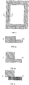
- FIG. 2 is a schematic structural plan view of the mask provided by the embodiment of the present disclosure.
- FIGS. 2a and 2b are schematic structural sectional views of the mask as illustrated in FIG. 2 .
- the mask 100 comprises a frame 101 and first mask strips 1021 disposed inside the frame 101.
- the frame 101 includes an outer frame 1011 and an inner frame 1012; the outer frame 1011 is disposed on the outer side and includes a first plane 103; the inner frame 1012 is disposed on the inner side and includes a second plane 104; the first plane 103 is higher than the second plane 104, relative to a bottom surface of the frame 101, so as to form a step 105; each first mask strip 1021 is fixed on the outer frame 1011 through two ends and is extended inside the outer frame 1011 along one side of the frame 101; and an orthographic projection of the first mask strip 1021 on the second plane 104 is partially overlapped with the inner frame 1012 on sides.
- first mask strips 1021 are arranged in the longitudinal direction and respectively disposed on the left side and the right side of the frame 101; and the first mask strips 1021 are respectively fixed on the outer frame 1011 through two end portions and respectively fixed inside the outer frame on the left side and the right side of the frame 101 (namely the main body except the end portions is disposed inside the outer frame), so the orthographic projection of the first mask strip 1021 on the second plane 104 is not overlapped with the outer frame 1011.
- the fixing means of the end portions of the first mask strip 1021 may include welding, riveting, etc.
- the inner frame 1012 and the outer frame 1011 are integrally formed; after a frame body is formed, the side of the outer frame closer to the area defined by the frame is etched to a certain thickness, so as to form the step 105 formed by the first plane 103 and the second plane 104, and the first plane 103 is higher than the second plane 104.
- the frame 101 may be formed in one piece by stamping.
- the inner frame 1012 and the outer frame 1011 are respectively formed and then connected with each other (e.g., by welding) to form a whole body including the first plane 103 and the second plane 104, and the first plane 103 is higher than the second plane 104, so as to form the step 105.
- the sectional view along A-A1 in FIG. 2 is also different. It should be noted that the section line A-A1 is a center line of the first mask strip 1021. For instance, as illustrated in FIG.
- the first mask strip 1021 is lapped over the outer frame 1011 and mounted above the inner frame 1012 and the step 105; and in the direction perpendicular to the extension direction of the first mask strip 1021, one part of an orthographic projection of the first mask strip 1021 on the second plane 104 is overlapped with the inner frame 1012 on one side, and the other part falls within an area defined by the inner frame 1012.
- the height difference h between the first plane 103 and the second plane 104 is 1 mm - 10 mm.
- the height difference h between the first plane 103 and the second plane 104 is 5 mm.
- the degree of freedom of the first mask strip is not limited.
- the distance L between the main body of the first mask strip 1021 and the outer frame 1011 is 0.5 mm - 2 mm.
- L is 1 mm.
- the first mask strip 1021 is fixed on the outer frame by means of welding.
- the welding includes spot welding, etc.
- the mask 100 may further comprise second mask strips 1022 disposed on the inner side of the frame 101.
- the second mask strips 1022 are fixed on the outer frame 1011 and extended inside the outer frame 1011 along the other side of the frame 101.
- an orthographic projection of each second mask strip 1022 on the second plane 104 is at least partially overlapped with the inner frame 1012 on the other side.
- the partial overlap here includes the overlap of orthographic projections of end portions of the second mask strip 1022 on the second plane 104 and the inner frame 1012 on the other side, and the overlap of an orthographic projection of a main body of the second mask strip 1022 on the second plane 104 and the inner frame 1012 on the other side.
- two second mask strips are transversely arranged on the upper side and the lower side of the frame 101 respectively.
- the second mask strips 1022 are respectively fixed on the outer frame 1011 through two end portions, and respectively disposed inside the outer frame on the upper side and the lower side of the frame 101 (namely a main body except the end portions is disposed inside the outer frame), so there is no overlapped area between the orthographic projection of the second mask strip 1022 on the second plane 104 and the outer frame 1011.
- the fixing means of the end portions of the second mask strip 1022 may include welding, riveting, etc.
- second mask strips 1022 are also included and disposed in the middle of the frame 101.
- These second mask strips 1022 are fixed on the outer frame 1011 through two end portions and intersected with the middle of the first mask strips 1021, so as to divide the area encircled by the frame into a plurality of sub-areas.
- the size of the sub-areas formed here may be same or different.
- a plurality of first mask strips 1021 may also be fixed on the outer frame so as to divide an area encircled by the frame 101 into more sub-areas.
- the thickness at the overlapped area is the sum of the thickness of the second mask strip 1022 and the first mask strip 1021, namely the second mask strip 1022 and the first mask strip 1021 make contact with each other.
- the first mask strip 1021 and the second mask strip 1022 have an equal thickness, and are respectively etched by a half of the thickness at the intersected area.
- the thickness at the intersected area is the thickness of one mask strip.
- both the thicknesses of the first mask strip 1021 and the thickness of the second mask strip 1022 are 50 ⁇ m - 100 ⁇ m, e.g., 50 ⁇ m, 75 ⁇ m or 100 ⁇ m.
- first mask strips 1021 and the second mask strips 1022 as illustrated in FIGS. 2 and 3 are only illustrative and obviously not limited to the case as illustrated in FIG. 2 .
- a plurality of mask strips 1021 or a plurality of second mask strips 1022 may also be disposed in the area defined by the frame as required so as to form required film forming areas.
- other first mask strip(s) 1021 may also be disposed at the middle part of the frame in the transverse direction.
- FIG. 4 is a schematic structural plan view of the frame in the embodiment of the present disclosure.
- FIGS. 4a-4d are schematic structural sectional views of the frame as illustrated in FIG. 4 .
- an orthographic projection of the inner frame on the first plane is in butt joint with one side of the outer frame; or as illustrated in FIGS. 4b and 4c , the orthographic projection of the inner frame on the first frame is at least partially overlapped with one side of the outer frame; or as illustrated in FIG 4d , one surface of the inner frame, opposite to the second plane, is set to be in the shape of an inclined slope, so as to provide convenience for the uniform coating of an evaporation material(s) at edge areas during evaporation.
- An embodiment of the present disclosure further provides an evaporation device, which comprises the mask provided by the first embodiment.
- FIG. 5a is a schematic structural plan view of the mask
- FIG. 5b is a schematic structural sectional view when the mask as illustrated in FIG. 5 is applied to the evaporation device.
- the section of the mask in FIG. 5b is cut along D-D1 line in FIG. 5a .
- the evaporation device further comprises a magnet 201 arranged opposite to the mask.
- the magnet and the mask 100 are respectively disposed on both sides of a glass substrate 202 to be evaporated.
- the first mask strips 1021 are made from magnetic materials, e.g., iron (Fe), nickel (Ni) or Fe-Ni alloy materials. The first mask strips are closely attached to the glass substrate for evaporation under the action of the magnetic force of the magnet 201 on the first mask strips.
- the second mask strips also have magnetic property;
- the second mask strip is fixed on the outer frame through two ends; a plurality of second mask strips may also be arranged; the second mask strips may be intersected with the middle parts of the first mask strips so as to divide the area encircled by the frame into a plurality of sub-areas; and the first mask strips and the second mask strips are closely attached to the glass substrate for evaporation under the action of the magnetic force of the magnet on the first mask strips and the second mask strips, so as to form a plurality of film forming areas.
- the mask and the evaporation device have the following advantages: the structure of the frame is modified and designed into having two planes with different heights, so as to form a step; subsequently, the first mask strips are lapped over the frame; and two ends of each first mask strip are fixed on the outer frame, but the main body does not make contact with the frame so as to avoid the problem that the glass substrate is scratched by the first mask strips and effectively improve the yield and the service life of subsequent products.
Landscapes
- Chemical & Material Sciences (AREA)
- Chemical Kinetics & Catalysis (AREA)
- Engineering & Computer Science (AREA)
- Materials Engineering (AREA)
- Mechanical Engineering (AREA)
- Metallurgy (AREA)
- Organic Chemistry (AREA)
- Physical Vapour Deposition (AREA)
- Electroluminescent Light Sources (AREA)
Abstract
Description
- Embodiments of the present disclosure relate to a mask and an evaporation device.
- Evaporation process is widely applied in the coating process for electronic devices. The principle of the evaporation process is to place a substrate for evaporation in a vacuum environment and deposit an evaporation material(s) on a surface of the substrate for evaporation for forming of film. Film formation areas of the substrate for evaporation are usually defined by mask strips.
- In the evaporation process, if the edge of the substrate is scratched, the problems such as breakage of a peripheral circuit and package failure can be easily caused, so the yield and the service life of products can be disadvantageously affected. The scratching of the edge of the substrate is usually caused by the relative motion between the mask strips and the glass substrate during contact.
- Currently, in order to solve the problem that the substrate can be easily scratched, on one hand, the sharpness and the roughness of edges of the mask strips are effectively controlled; and on the other hand, the relative motion between the mask strips and the glass substrate is slowed down, and the mutual acting force of the mask strips and the glass substrate is weakened. However, in order to ensure the flatness requirement in the contact of the mask strips and the glass substrate, the thickness of the mask strips is generally 100µm or less, so the edges of the mask strips will be inevitably sharp. The mask strips are manufactured by an etching process, and it is greatly difficult to control the sharpness and the roughness of the edges of the mask strips by adjusting the parameters of the etching process.
- At least embodiment of the present disclosure provides a mask, including a frame and a first mask strip disposed inside the frame; the frame includes an outer frame and an inner frame; the outer frame is disposed on an outer side and includes a first plane; the inner frame is disposed on an inner side and includes a second plane; the first plane is higher than the second plane so as to form a step; the first mask strip is fixed on the outer frame through two ends and extended inside the outer frame along one side of the frame; and an orthographic projection of the first mask strip on the second plane is at least partially overlapped with the inner frame on the one side.
- For example, in the mask in an embodiment of the present disclosure, a height difference between the first plane and the second plane is 1 mm - 10 mm.
- For example, in the mask in an embodiment of the present disclosure, the height difference between the first plane and the second plane is 5 mm.
- For example, in the mask in an embodiment of the present disclosure, on the first plane and in a direction perpendicular to an extension direction of the first mask strip, the distance between a main body of the first mask strip and the outer frame is 0.5 mm - 2 mm.
- For example, the mask in an embodiment of the present disclosure further comprises a second mask strip disposed inside the frame.
- For example, in the mask in an embodiment of the present disclosure, the second mask strip is fixed on the outer frame through two ends and extended inside the outer frame along an other side of the frame; and an orthographic projection of the second mask strip on the second plane is at least partially overlapped with the inner frame on the other side.
- For example, in the mask in an embodiment of the present disclosure, there is an overlapped area between the second mask strip and the first mask strip.
- For example, in the mask in an embodiment of the present disclosure, the second mask strip is fixed on the outer frame through two ends; and the second mask strip is intersected with a middle part of the first mask strip so as to divide an area encircled by the frame into a plurality of sub-areas.
- For example, in the mask in an embodiment of the present disclosure, the first mask strip and the second mask strip have an equal thickness.
- For example, in the mask in an embodiment of the present disclosure, both the thicknesses of the first mask strip and the thickness of the second mask strip are 50 µm - 100 µm.
- At least embodiment of the present disclosure provides an evaporation device comprising any mask that is described above.
- For example, in an embodiment of the present disclosure, the evaporation device further comprises a magnet arranged opposite to the mask, the first mask strip has a magnetic property and is capable of being attracted by the magnet to move.
- In order to clearly illustrate the technical solution of the embodiments of the disclosure, the drawings of the embodiments will be briefly described in the following; it is obvious that the described drawings are only related to some embodiments of the disclosure and thus are not limitative of the disclosure.
-
FIG 1 is a schematic structural plan view of a mask; -
FIG. 2 is a schematic structural plan view of a mask provided by an embodiment of the present disclosure; -
FIGS. 2a-2b are schematic structural sectional views of the mask as illustrated inFIG. 2 ; -
FIG. 3 is a schematic structural plan view of a mask provided by an embodiment of the present disclosure; -
FIG. 3a is a schematic structural sectional view of the mask as illustrated inFIG. 3 ; -
FIG. 4 is a schematic structural plan view of a frame in an embodiment of the present disclosure; -
FIGS. 4a-4d are schematic structural sectional views of the frame as illustrated inFIG. 4 ; -
FIG. 5a is a schematic structural plan view of a mask; and -
FIG. 5b is a schematic structural sectional view when the mask as illustrated inFIG. 5a is applied to an evaporation device. - In order to make objects, technical details and advantages of the embodiments of the disclosure apparent, the technical solutions of the embodiments will be described in a clearly and fully understandable way in connection with the drawings related to the embodiments of the disclosure. Apparently, the described embodiments are just a part but not all of the embodiments of the disclosure. Based on the described embodiments herein, those skilled in the art can obtain other embodiment(s), without any inventive work, which should be within the scope of the disclosure.
- Unless otherwise defined, all the technical and scientific terms used herein have the same meanings as commonly understood by one of ordinary skill in the art to which the present disclosure belongs. The terms "first," "second," etc., which are used in the description and the claims of the present application for disclosure, are not intended to indicate any sequence, amount or importance, but distinguish various components. Also, the terms such as "a," "an," etc., are not intended to limit the amount, but indicate the existence of at least one. The terms "comprise," "comprising," "include," "including," etc., are intended to specify that the elements or the objects stated before these terms encompass the elements or the objects and equivalents thereof listed after these terms, but do not preclude the other elements or objects. The phrases "connect", "connected", etc., are not intended to define a physical connection or mechanical connection, but may include an electrical connection, directly or indirectly. "On," "under," "right," "left" and the like are only used to indicate relative position relationship, and when the position of the object which is described is changed, the relative position relationship may be changed accordingly.
-
FIG. 1 is a schematic structural plan view of a mask. As illustrated inFIG. 1 , themask 100 comprises aframe 101 andmask strips 102 fixed on theframe 101. As can be seen fromFIG. 1 , themask 100 comprises sixmask strips 102, four mask strips of which are fixed at the periphery of theframe 101 and make direct contact with the frame; orthographic projections of the four mask strips on a plane in which the frame is provided are overlapped with the frame; and the rest two mask strips are lapped over theframe 101. The inventors have noted in research that: the four mask strips fixed at the periphery of theframe 101 are key reasons in causing the scratching of the substrate; and as the main bodies of the peripheral mask strips make direct contact with theframe 101, when the peripheral mask strips are attracted by the magnetic force of magnets, the tilting motion of the mask strips is limited, so the probability that the mask strips move upwards and scratch the glass substrate is increased, namely the degree of freedom of the mask strips is limited, so the mutual acting force between the mask strips and the glass substrate is increased, and hence the glass substrate can be scratched. From the aspect of increasing the degree of freedom of the mask strips, the problem of the scratching of the edge of the substrate can be solved by slowing down the relative motion between the mask strips and the glass substrate. For instance, if the peripheral four mask strips are also manufactured to be lapped over the frame as the other two mask strips, the problem that the glass substrate is scratched by the mask strips can be obviously reduced. However, in this case, this configuration brings about the film leakage phenomenon during evaporation, so the product yield can be reduced. In order to solve the above problem, in the present disclosure, the structure of the frame is modified and designed have two planes with different heights so as to form a step(s); and first mask strips are lapped over an outer frame of the frame, so the main bodies of the first mask strips will not make contact with the frame. Thus, the present disclosure avoids the problem that the glass substrate is scratched by the first mask strips, and effectively improves the yield and the service life of subsequent products. - At least one embodiment of the present disclosure provides a mask, which comprises a frame and a first mask strip disposed inside the frame. The frame includes an outer frame that is disposed on the outer side and includes a first plane and an inner frame that is disposed on the inner side and includes a second plane; the first plane is higher than the second plane so as to form a step; the first mask strip is fixed on the outer frame through two ends and is extended inside the outer frame along one side of the frame; and an orthographic projection of the first mask strip on the second plane is at least partially overlapped with the inner frame on one side.
- An embodiment of the present disclosure provides a mask.
FIG. 2 is a schematic structural plan view of the mask provided by the embodiment of the present disclosure.FIGS. 2a and 2b are schematic structural sectional views of the mask as illustrated inFIG. 2 . - As shown in
FIGS. 2, 2a and 2b , themask 100 comprises aframe 101 andfirst mask strips 1021 disposed inside theframe 101. Theframe 101 includes anouter frame 1011 and aninner frame 1012; theouter frame 1011 is disposed on the outer side and includes afirst plane 103; theinner frame 1012 is disposed on the inner side and includes asecond plane 104; thefirst plane 103 is higher than thesecond plane 104, relative to a bottom surface of theframe 101, so as to form astep 105; eachfirst mask strip 1021 is fixed on theouter frame 1011 through two ends and is extended inside theouter frame 1011 along one side of theframe 101; and an orthographic projection of thefirst mask strip 1021 on thesecond plane 104 is partially overlapped with theinner frame 1012 on sides. InFIG. 2 , twofirst mask strips 1021 are arranged in the longitudinal direction and respectively disposed on the left side and the right side of theframe 101; and thefirst mask strips 1021 are respectively fixed on theouter frame 1011 through two end portions and respectively fixed inside the outer frame on the left side and the right side of the frame 101 (namely the main body except the end portions is disposed inside the outer frame), so the orthographic projection of thefirst mask strip 1021 on thesecond plane 104 is not overlapped with theouter frame 1011. The fixing means of the end portions of thefirst mask strip 1021 may include welding, riveting, etc. - For instance, the
inner frame 1012 and theouter frame 1011 are integrally formed; after a frame body is formed, the side of the outer frame closer to the area defined by the frame is etched to a certain thickness, so as to form thestep 105 formed by thefirst plane 103 and thesecond plane 104, and thefirst plane 103 is higher than thesecond plane 104. Or theframe 101 may be formed in one piece by stamping. Or theinner frame 1012 and theouter frame 1011 are respectively formed and then connected with each other (e.g., by welding) to form a whole body including thefirst plane 103 and thesecond plane 104, and thefirst plane 103 is higher than thesecond plane 104, so as to form thestep 105. - For instance, as for the cases where the overlapped area between the orthographic projection of the
first mask strip 1021 on thesecond plane 104 and theinner frame 1012 on one side has different sizes, the sectional view along A-A1 inFIG. 2 is also different. It should be noted that the section line A-A1 is a center line of thefirst mask strip 1021. For instance, as illustrated inFIG. 2a , when the overlapped area between thefirst mask strip 1021 and theinner frame 1012 is small and does not exceed beyond the center line of the first mask strip, there are partially overlapped areas between orthographic projections of the two end portions of thefirst mask 1021 and theinner frame 1012 on one side, namely the orthographic projections of the end portions of thefirst mask strip 1021 on thesecond plane 104 are overlapped with theinner frame 1012 on one side. As illustrated inFIG. 2b , when the overlapped area between thefirst mask strip 1021 and theinner frame 1012 is large and exceeds beyond the center line of the first mask strip, there are overlapped areas between orthographic projections of the main body and the two end portions of thefirst mask strip 1021 on thesecond plane 104 and theinner frame 1012 on one side. As can be seen fromFIGS. 2a and 2b , thefirst mask strip 1021 is lapped over theouter frame 1011 and mounted above theinner frame 1012 and thestep 105; and in the direction perpendicular to the extension direction of thefirst mask strip 1021, one part of an orthographic projection of thefirst mask strip 1021 on thesecond plane 104 is overlapped with theinner frame 1012 on one side, and the other part falls within an area defined by theinner frame 1012. - For instance, as illustrated in
FIG 2a or 2b , the height difference h between thefirst plane 103 and thesecond plane 104 is 1 mm - 10 mm. Illustratively, the height difference h between thefirst plane 103 and thesecond plane 104 is 5 mm. Within the height difference range, when thefirst mask strip 1021 moves under the action of an external acting force, the main body of the first mask strip does not make contact with the inner frame, so the degree of freedom of the first mask strip is not limited. - For instance, as illustrated in
FIG. 2 , on thefirst plane 103 and in the direction perpendicular to the extension direction of thefirst mask strip 1021, the distance L between the main body of thefirst mask strip 1021 and theouter frame 1011 is 0.5 mm - 2 mm. Illustratively, L is 1 mm. Within the range of L, when thefirst mask strip 1021 makes contact with theouter frame 1011 under the action of the external acting force, the problem of increasing the scratch degree of the glass substrate will not occur. - For instance, the
first mask strip 1021 is fixed on the outer frame by means of welding. The welding includes spot welding, etc. - For instance, as illustrated in
FIG. 2 , themask 100 may further comprise second mask strips 1022 disposed on the inner side of theframe 101. The second mask strips 1022 are fixed on theouter frame 1011 and extended inside theouter frame 1011 along the other side of theframe 101. As similar to thefirst mask strips 1021 as described above, an orthographic projection of eachsecond mask strip 1022 on thesecond plane 104 is at least partially overlapped with theinner frame 1012 on the other side. For instance, the partial overlap here includes the overlap of orthographic projections of end portions of thesecond mask strip 1022 on thesecond plane 104 and theinner frame 1012 on the other side, and the overlap of an orthographic projection of a main body of thesecond mask strip 1022 on thesecond plane 104 and theinner frame 1012 on the other side. - In
FIG. 2 , two second mask strips are transversely arranged on the upper side and the lower side of theframe 101 respectively. The second mask strips 1022 are respectively fixed on theouter frame 1011 through two end portions, and respectively disposed inside the outer frame on the upper side and the lower side of the frame 101 (namely a main body except the end portions is disposed inside the outer frame), so there is no overlapped area between the orthographic projection of thesecond mask strip 1022 on thesecond plane 104 and theouter frame 1011. The fixing means of the end portions of thesecond mask strip 1022 may include welding, riveting, etc. - For instance, as illustrated in
FIG. 2 , other transversely extended second mask strips 1022 are also included and disposed in the middle of theframe 101. These second mask strips 1022 are fixed on theouter frame 1011 through two end portions and intersected with the middle of the first mask strips 1021, so as to divide the area encircled by the frame into a plurality of sub-areas. According to actual demands, the size of the sub-areas formed here may be same or different. For instance, a plurality offirst mask strips 1021 may also be fixed on the outer frame so as to divide an area encircled by theframe 101 into more sub-areas. - For instance, as illustrated in
FIG. 2 , there are overlapped areas between the second mask strips 1022 and the first mask strips 1021. The thickness at the overlapped area is the sum of the thickness of thesecond mask strip 1022 and thefirst mask strip 1021, namely thesecond mask strip 1022 and thefirst mask strip 1021 make contact with each other. - For instance, as illustrated in
FIGS. 3 and 3a , thefirst mask strip 1021 and thesecond mask strip 1022 have an equal thickness, and are respectively etched by a half of the thickness at the intersected area. The thickness at the intersected area is the thickness of one mask strip. Thus, when thefirst mask strips 1021 and the second mask strips 1022 are closely attached to a substrate for evaporation, the problem of uneven evaporated film on the substrate due to unevenness at the intersected areas does not occur. - For instance, both the thicknesses of the
first mask strip 1021 and the thickness of thesecond mask strip 1022 are 50 µm - 100 µm, e.g., 50 µm, 75 µm or 100 µm. - It should be noted that the numbers of the
first mask strips 1021 and the second mask strips 1022 as illustrated inFIGS. 2 and3 are only illustrative and obviously not limited to the case as illustrated inFIG. 2 . A plurality ofmask strips 1021 or a plurality of second mask strips 1022 may also be disposed in the area defined by the frame as required so as to form required film forming areas. For instance, other first mask strip(s) 1021 may also be disposed at the middle part of the frame in the transverse direction. -
FIG. 4 is a schematic structural plan view of the frame in the embodiment of the present disclosure.FIGS. 4a-4d are schematic structural sectional views of the frame as illustrated inFIG. 4 . As illustrated inFIG. 4a , an orthographic projection of the inner frame on the first plane is in butt joint with one side of the outer frame; or as illustrated inFIGS. 4b and 4c , the orthographic projection of the inner frame on the first frame is at least partially overlapped with one side of the outer frame; or as illustrated inFIG 4d , one surface of the inner frame, opposite to the second plane, is set to be in the shape of an inclined slope, so as to provide convenience for the uniform coating of an evaporation material(s) at edge areas during evaporation. - An embodiment of the present disclosure further provides an evaporation device, which comprises the mask provided by the first embodiment.
- For instance,
FIG. 5a is a schematic structural plan view of the mask, andFIG. 5b is a schematic structural sectional view when the mask as illustrated inFIG. 5 is applied to the evaporation device. For instance, the section of the mask inFIG. 5b is cut along D-D1 line inFIG. 5a . - For instance, as illustrated in
FIG. 5b , the evaporation device further comprises amagnet 201 arranged opposite to the mask. At this point, the magnet and themask 100 are respectively disposed on both sides of aglass substrate 202 to be evaporated. In this case, thefirst mask strips 1021 are made from magnetic materials, e.g., iron (Fe), nickel (Ni) or Fe-Ni alloy materials. The first mask strips are closely attached to the glass substrate for evaporation under the action of the magnetic force of themagnet 201 on the first mask strips. - For instance, the second mask strips also have magnetic property; the second mask strip is fixed on the outer frame through two ends; a plurality of second mask strips may also be arranged; the second mask strips may be intersected with the middle parts of the first mask strips so as to divide the area encircled by the frame into a plurality of sub-areas; and the first mask strips and the second mask strips are closely attached to the glass substrate for evaporation under the action of the magnetic force of the magnet on the first mask strips and the second mask strips, so as to form a plurality of film forming areas.
- The mask and the evaporation device, provided by an embodiment of the present disclosure, have the following advantages: the structure of the frame is modified and designed into having two planes with different heights, so as to form a step; subsequently, the first mask strips are lapped over the frame; and two ends of each first mask strip are fixed on the outer frame, but the main body does not make contact with the frame so as to avoid the problem that the glass substrate is scratched by the first mask strips and effectively improve the yield and the service life of subsequent products.
- The following points should be noted:
- (1) The accompanying drawings in the embodiments of the present disclosure only involve structures relevant to the embodiments of the present disclosure, and other structures may refer to the art of state.
- (2) For clarity, in the accompanying drawings of the embodiments of the present disclosure, the thickness of layers or regions is enlarged or reduced, namely the accompanying drawings are not drawn according to actual scales. It should be understood that: when an element such as a layer, a film, a region or a substrate is referred to as being disposed "on" or "beneath" another element, the element may be "directly" disposed "on" or "beneath" another element, or an intermediate element may be provided.
- (3) The embodiments of the present disclosure and the characteristics in the embodiments may be mutually combined to obtain new embodiments without conflict.
- The foregoing is only the preferred embodiments of the present disclosure and not intended to limit the scope of protection of the present disclosure. The scope of protection of the present disclosure should be defined by the appended claims.
- The application claims priority to the Chinese patent application No.
201620851904.X, filed August 8, 2016
Claims (12)
- A mask, comprising a frame and a first mask strip disposed inside the frame, wherein
the frame includes an outer frame and an inner frame; the outer frame is disposed on an outer side and includes a first plane; the inner frame is disposed on an inner side and includes a second plane; the first plane is higher than the second plane so as to form a step;
the first mask strip is fixed on the outer frame through two ends and extended inside the outer frame along one side of the frame; and an orthographic projection of the first mask strip on the second plane is at least partially overlapped with the inner frame on the one side. - The mask according to claim 1, wherein a height difference between the first plane and the second plane is 1 mm - 10 mm.
- The mask according to claim 2, wherein the height difference between the first plane and the second plane is 5 mm.
- The mask according to claim 1, wherein on the first plane and in a direction perpendicular to an extension direction of the first mask strip, the distance between a main body of the first mask strip and the outer frame is 0.5 mm - 2 mm.
- The mask according to any one of claims 1 to 4, further comprising a second mask strip disposed inside the frame.
- The mask according to claim 5, wherein the second mask strip is fixed on the outer frame through two ends and extended inside the outer frame along an other side of the frame; and an orthographic projection of the second mask strip on the second plane is at least partially overlapped with the inner frame on the other side.
- The mask according to claim 5, wherein there is an overlapped area between the second mask strip and the first mask strip.
- The mask according to claim 7, wherein the second mask strip is fixed on the outer frame through two ends; and the second mask strip is intersected with a middle part of the first mask strip so as to divide an area encircled by the frame into a plurality of sub-areas.
- The mask according to claim 7 or 8, wherein the first mask strip and the second mask strip have an equal thickness.
- The mask according to any one of claims 6 to 8, wherein both the thicknesses of the first mask strip and the thickness of the second mask strip are 50 µm - 100 µm.
- An evaporation device, comprising the mask according to any one of claims 1 to 10.
- The evaporation device according to claim 11, further comprising a magnet arranged opposite to the mask,
wherein the first mask strip has a magnetic property and is capable of being attracted by the magnet to move.
Applications Claiming Priority (2)
| Application Number | Priority Date | Filing Date | Title |
|---|---|---|---|
| CN201620851904.XU CN205856592U (en) | 2016-08-08 | 2016-08-08 | Mask plate and evaporation coating device |
| PCT/CN2017/075341 WO2018028183A1 (en) | 2016-08-08 | 2017-03-01 | Mask plate and evaporation device |
Publications (3)
| Publication Number | Publication Date |
|---|---|
| EP3498880A1 true EP3498880A1 (en) | 2019-06-19 |
| EP3498880A4 EP3498880A4 (en) | 2020-04-08 |
| EP3498880B1 EP3498880B1 (en) | 2023-05-10 |
Family
ID=57657888
Family Applications (1)
| Application Number | Title | Priority Date | Filing Date |
|---|---|---|---|
| EP17767720.0A Active EP3498880B1 (en) | 2016-08-08 | 2017-03-01 | Mask plate and evaporation device |
Country Status (4)
| Country | Link |
|---|---|
| US (1) | US10465277B2 (en) |
| EP (1) | EP3498880B1 (en) |
| CN (1) | CN205856592U (en) |
| WO (1) | WO2018028183A1 (en) |
Families Citing this family (13)
| Publication number | Priority date | Publication date | Assignee | Title |
|---|---|---|---|---|
| CN205856592U (en) | 2016-08-08 | 2017-01-04 | 合肥鑫晟光电科技有限公司 | Mask plate and evaporation coating device |
| JP6919145B2 (en) * | 2017-08-09 | 2021-08-18 | 株式会社飯沼ゲージ製作所 | Mask manufacturing equipment and mask manufacturing method |
| CN108004503B (en) * | 2017-12-15 | 2021-01-19 | 京东方科技集团股份有限公司 | Mask plate, evaporation equipment and device |
| CN110184582B (en) * | 2018-02-23 | 2021-09-14 | 京东方科技集团股份有限公司 | Mask plate, manufacturing method thereof and display device |
| CN108998773B (en) * | 2018-07-27 | 2023-08-18 | 京东方科技集团股份有限公司 | Mask plate, manufacturing method thereof and packaging equipment |
| CN109599477B (en) * | 2018-11-28 | 2020-06-02 | 武汉华星光电技术有限公司 | How to make a mesh |
| JP7406719B2 (en) * | 2019-01-29 | 2023-12-28 | 大日本印刷株式会社 | Vapor deposition mask and manufacturing method thereof, vapor deposition mask device and manufacturing method thereof, intermediate, vapor deposition method, and manufacturing method of organic EL display device |
| CN111074204B (en) * | 2020-01-03 | 2022-01-14 | 京东方科技集团股份有限公司 | Mask plate and manufacturing method thereof |
| CN111088474B (en) * | 2020-01-03 | 2022-07-05 | 京东方科技集团股份有限公司 | Mask plate and manufacturing method thereof |
| CN111676446B (en) * | 2020-06-24 | 2022-10-28 | 京东方科技集团股份有限公司 | Mask plate, mask plate structure and mask plate manufacturing method |
| CN112176282B (en) * | 2020-08-27 | 2023-02-10 | 合肥维信诺科技有限公司 | Mask and evaporation device |
| KR102929156B1 (en) * | 2020-08-31 | 2026-02-24 | 삼성디스플레이 주식회사 | Mask, method of manufacturing the same, and method of manufacturing display panel |
| CN116121698B (en) * | 2023-01-18 | 2025-07-29 | 合肥维信诺科技有限公司 | Mask assembly and mask plate |
Family Cites Families (13)
| Publication number | Priority date | Publication date | Assignee | Title |
|---|---|---|---|---|
| US3323490A (en) * | 1966-02-21 | 1967-06-06 | Trw Inc | Adjustable mask |
| TW504605B (en) * | 1999-12-03 | 2002-10-01 | Asm Lithography Bv | Lithographic projection apparatus, method of manufacturing a device using the same, the device and mask |
| TWI412621B (en) * | 2004-07-16 | 2013-10-21 | Applied Materials Inc | Shadow frame with mask panels |
| US7821199B2 (en) * | 2004-09-08 | 2010-10-26 | Toray Industries, Inc. | Organic electroluminescent device and manufacturing method thereof |
| JP4773834B2 (en) * | 2006-02-03 | 2011-09-14 | キヤノン株式会社 | Mask film forming method and mask film forming apparatus |
| JP2008031528A (en) * | 2006-07-28 | 2008-02-14 | Kyocera Corp | CVD mask and display manufacturing method using the same |
| JP2010135269A (en) * | 2008-12-08 | 2010-06-17 | Sony Corp | Mask for vapor deposition |
| KR101041138B1 (en) * | 2009-03-03 | 2011-06-13 | 삼성모바일디스플레이주식회사 | Deposition Mask |
| JP2012092395A (en) * | 2010-10-27 | 2012-05-17 | Canon Inc | Film formation method and film formation apparatus |
| CN103668051A (en) | 2012-09-07 | 2014-03-26 | 昆山允升吉光电科技有限公司 | Mask frame and corresponding mask component thereof for vapor deposition |
| CN103668053A (en) * | 2012-09-07 | 2014-03-26 | 昆山允升吉光电科技有限公司 | Mask frame and corresponding mask component thereof |
| JP5846287B1 (en) * | 2013-12-27 | 2016-01-20 | 大日本印刷株式会社 | Manufacturing method of vapor deposition mask with frame, tension device, manufacturing apparatus of organic semiconductor element, and manufacturing method of organic semiconductor element |
| CN205856592U (en) * | 2016-08-08 | 2017-01-04 | 合肥鑫晟光电科技有限公司 | Mask plate and evaporation coating device |
-
2016
- 2016-08-08 CN CN201620851904.XU patent/CN205856592U/en active Active
-
2017
- 2017-03-01 US US15/561,716 patent/US10465277B2/en active Active
- 2017-03-01 EP EP17767720.0A patent/EP3498880B1/en active Active
- 2017-03-01 WO PCT/CN2017/075341 patent/WO2018028183A1/en not_active Ceased
Also Published As
| Publication number | Publication date |
|---|---|
| CN205856592U (en) | 2017-01-04 |
| WO2018028183A1 (en) | 2018-02-15 |
| EP3498880B1 (en) | 2023-05-10 |
| EP3498880A4 (en) | 2020-04-08 |
| US20180245198A1 (en) | 2018-08-30 |
| US10465277B2 (en) | 2019-11-05 |
Similar Documents
| Publication | Publication Date | Title |
|---|---|---|
| EP3498880B1 (en) | Mask plate and evaporation device | |
| US11871647B2 (en) | Flexible substrate, manufacturing method for flexible substrate and display device | |
| US12508797B2 (en) | Deposition mask package and deposition mask packaging method | |
| CN211713188U (en) | Vapor deposition mask device and mask support mechanism | |
| JP2022179744A (en) | Frame-integrated vapor deposition mask, method for manufacturing organic semiconductor element, and method for forming pattern | |
| KR102218952B1 (en) | Deposition mask, preparatory body for deposition mask, method for manufacturing deposition mask, and method for manufacturing organic semiconductor element | |
| JP4669069B2 (en) | Mesh sheet and housing parts for electronic devices | |
| US12035497B2 (en) | Display device | |
| KR20210013337A (en) | Vapor deposition mask, vapor deposition mask precursor, vapor deposition mask manufacturing method, and organic semiconductor element manufacturing method | |
| US20160333457A1 (en) | Mask plate, method for fabricating the same, display panel and display device | |
| US10890946B2 (en) | Stacking structure for flexible display assembly | |
| WO2018019045A1 (en) | Mask, preparation method therefor, and mask frame assembly | |
| KR102631580B1 (en) | Mask and its manufacturing method | |
| EP3444845A1 (en) | Method for manufacturing display substrate, display substrate, and display device | |
| US11560616B2 (en) | Mask device, mask plate, and frame | |
| KR20200079442A (en) | Vapor deposition mask | |
| CN107863433A (en) | Display device and display panel | |
| CN110684952A (en) | Target material structure | |
| KR101415805B1 (en) | Method for enhancing mechanical strength of glass | |
| US20210214835A1 (en) | Mask sheet, mask component, and vapor-deposition method | |
| TWI530398B (en) | Display panel | |
| CN112662993B (en) | Mask plate, evaporation device and evaporation method | |
| KR102753719B1 (en) | Folding plate and manufacturing method thereof | |
| CN115882211A (en) | Antenna, manufacturing method thereof and display device | |
| CN110724928A (en) | mask |
Legal Events
| Date | Code | Title | Description |
|---|---|---|---|
| STAA | Information on the status of an ep patent application or granted ep patent |
Free format text: STATUS: UNKNOWN |
|
| STAA | Information on the status of an ep patent application or granted ep patent |
Free format text: STATUS: THE INTERNATIONAL PUBLICATION HAS BEEN MADE |
|
| PUAI | Public reference made under article 153(3) epc to a published international application that has entered the european phase |
Free format text: ORIGINAL CODE: 0009012 |
|
| STAA | Information on the status of an ep patent application or granted ep patent |
Free format text: STATUS: REQUEST FOR EXAMINATION WAS MADE |
|
| 17P | Request for examination filed |
Effective date: 20170925 |
|
| AK | Designated contracting states |
Kind code of ref document: A1 Designated state(s): AL AT BE BG CH CY CZ DE DK EE ES FI FR GB GR HR HU IE IS IT LI LT LU LV MC MK MT NL NO PL PT RO RS SE SI SK SM TR |
|
| AX | Request for extension of the european patent |
Extension state: BA ME |
|
| DAV | Request for validation of the european patent (deleted) | ||
| DAX | Request for extension of the european patent (deleted) | ||
| A4 | Supplementary search report drawn up and despatched |
Effective date: 20200311 |
|
| RIC1 | Information provided on ipc code assigned before grant |
Ipc: C23C 14/04 20060101AFI20200305BHEP Ipc: C23C 14/24 20060101ALI20200305BHEP |
|
| GRAP | Despatch of communication of intention to grant a patent |
Free format text: ORIGINAL CODE: EPIDOSNIGR1 |
|
| STAA | Information on the status of an ep patent application or granted ep patent |
Free format text: STATUS: GRANT OF PATENT IS INTENDED |
|
| INTG | Intention to grant announced |
Effective date: 20221201 |
|
| GRAS | Grant fee paid |
Free format text: ORIGINAL CODE: EPIDOSNIGR3 |
|
| GRAA | (expected) grant |
Free format text: ORIGINAL CODE: 0009210 |
|
| STAA | Information on the status of an ep patent application or granted ep patent |
Free format text: STATUS: THE PATENT HAS BEEN GRANTED |
|
| AK | Designated contracting states |
Kind code of ref document: B1 Designated state(s): AL AT BE BG CH CY CZ DE DK EE ES FI FR GB GR HR HU IE IS IT LI LT LU LV MC MK MT NL NO PL PT RO RS SE SI SK SM TR |
|
| REG | Reference to a national code |
Ref country code: GB Ref legal event code: FG4D |
|
| REG | Reference to a national code |
Ref country code: AT Ref legal event code: REF Ref document number: 1566741 Country of ref document: AT Kind code of ref document: T Effective date: 20230515 Ref country code: CH Ref legal event code: EP |
|
| REG | Reference to a national code |
Ref country code: DE Ref legal event code: R096 Ref document number: 602017068615 Country of ref document: DE |
|
| REG | Reference to a national code |
Ref country code: IE Ref legal event code: FG4D |
|
| REG | Reference to a national code |
Ref country code: LT Ref legal event code: MG9D |
|
| REG | Reference to a national code |
Ref country code: NL Ref legal event code: MP Effective date: 20230510 |
|
| REG | Reference to a national code |
Ref country code: AT Ref legal event code: MK05 Ref document number: 1566741 Country of ref document: AT Kind code of ref document: T Effective date: 20230510 |
|
| PG25 | Lapsed in a contracting state [announced via postgrant information from national office to epo] |
Ref country code: SE Free format text: LAPSE BECAUSE OF FAILURE TO SUBMIT A TRANSLATION OF THE DESCRIPTION OR TO PAY THE FEE WITHIN THE PRESCRIBED TIME-LIMIT Effective date: 20230510 Ref country code: PT Free format text: LAPSE BECAUSE OF FAILURE TO SUBMIT A TRANSLATION OF THE DESCRIPTION OR TO PAY THE FEE WITHIN THE PRESCRIBED TIME-LIMIT Effective date: 20230911 Ref country code: NO Free format text: LAPSE BECAUSE OF FAILURE TO SUBMIT A TRANSLATION OF THE DESCRIPTION OR TO PAY THE FEE WITHIN THE PRESCRIBED TIME-LIMIT Effective date: 20230810 Ref country code: NL Free format text: LAPSE BECAUSE OF FAILURE TO SUBMIT A TRANSLATION OF THE DESCRIPTION OR TO PAY THE FEE WITHIN THE PRESCRIBED TIME-LIMIT Effective date: 20230510 Ref country code: ES Free format text: LAPSE BECAUSE OF FAILURE TO SUBMIT A TRANSLATION OF THE DESCRIPTION OR TO PAY THE FEE WITHIN THE PRESCRIBED TIME-LIMIT Effective date: 20230510 Ref country code: AT Free format text: LAPSE BECAUSE OF FAILURE TO SUBMIT A TRANSLATION OF THE DESCRIPTION OR TO PAY THE FEE WITHIN THE PRESCRIBED TIME-LIMIT Effective date: 20230510 |
|
| PG25 | Lapsed in a contracting state [announced via postgrant information from national office to epo] |
Ref country code: RS Free format text: LAPSE BECAUSE OF FAILURE TO SUBMIT A TRANSLATION OF THE DESCRIPTION OR TO PAY THE FEE WITHIN THE PRESCRIBED TIME-LIMIT Effective date: 20230510 Ref country code: PL Free format text: LAPSE BECAUSE OF FAILURE TO SUBMIT A TRANSLATION OF THE DESCRIPTION OR TO PAY THE FEE WITHIN THE PRESCRIBED TIME-LIMIT Effective date: 20230510 Ref country code: LV Free format text: LAPSE BECAUSE OF FAILURE TO SUBMIT A TRANSLATION OF THE DESCRIPTION OR TO PAY THE FEE WITHIN THE PRESCRIBED TIME-LIMIT Effective date: 20230510 Ref country code: LT Free format text: LAPSE BECAUSE OF FAILURE TO SUBMIT A TRANSLATION OF THE DESCRIPTION OR TO PAY THE FEE WITHIN THE PRESCRIBED TIME-LIMIT Effective date: 20230510 Ref country code: IS Free format text: LAPSE BECAUSE OF FAILURE TO SUBMIT A TRANSLATION OF THE DESCRIPTION OR TO PAY THE FEE WITHIN THE PRESCRIBED TIME-LIMIT Effective date: 20230910 Ref country code: HR Free format text: LAPSE BECAUSE OF FAILURE TO SUBMIT A TRANSLATION OF THE DESCRIPTION OR TO PAY THE FEE WITHIN THE PRESCRIBED TIME-LIMIT Effective date: 20230510 Ref country code: GR Free format text: LAPSE BECAUSE OF FAILURE TO SUBMIT A TRANSLATION OF THE DESCRIPTION OR TO PAY THE FEE WITHIN THE PRESCRIBED TIME-LIMIT Effective date: 20230811 |
|
| PG25 | Lapsed in a contracting state [announced via postgrant information from national office to epo] |
Ref country code: FI Free format text: LAPSE BECAUSE OF FAILURE TO SUBMIT A TRANSLATION OF THE DESCRIPTION OR TO PAY THE FEE WITHIN THE PRESCRIBED TIME-LIMIT Effective date: 20230510 |
|
| PG25 | Lapsed in a contracting state [announced via postgrant information from national office to epo] |
Ref country code: SK Free format text: LAPSE BECAUSE OF FAILURE TO SUBMIT A TRANSLATION OF THE DESCRIPTION OR TO PAY THE FEE WITHIN THE PRESCRIBED TIME-LIMIT Effective date: 20230510 |
|
| PG25 | Lapsed in a contracting state [announced via postgrant information from national office to epo] |
Ref country code: SM Free format text: LAPSE BECAUSE OF FAILURE TO SUBMIT A TRANSLATION OF THE DESCRIPTION OR TO PAY THE FEE WITHIN THE PRESCRIBED TIME-LIMIT Effective date: 20230510 Ref country code: SK Free format text: LAPSE BECAUSE OF FAILURE TO SUBMIT A TRANSLATION OF THE DESCRIPTION OR TO PAY THE FEE WITHIN THE PRESCRIBED TIME-LIMIT Effective date: 20230510 Ref country code: RO Free format text: LAPSE BECAUSE OF FAILURE TO SUBMIT A TRANSLATION OF THE DESCRIPTION OR TO PAY THE FEE WITHIN THE PRESCRIBED TIME-LIMIT Effective date: 20230510 Ref country code: EE Free format text: LAPSE BECAUSE OF FAILURE TO SUBMIT A TRANSLATION OF THE DESCRIPTION OR TO PAY THE FEE WITHIN THE PRESCRIBED TIME-LIMIT Effective date: 20230510 Ref country code: DK Free format text: LAPSE BECAUSE OF FAILURE TO SUBMIT A TRANSLATION OF THE DESCRIPTION OR TO PAY THE FEE WITHIN THE PRESCRIBED TIME-LIMIT Effective date: 20230510 Ref country code: CZ Free format text: LAPSE BECAUSE OF FAILURE TO SUBMIT A TRANSLATION OF THE DESCRIPTION OR TO PAY THE FEE WITHIN THE PRESCRIBED TIME-LIMIT Effective date: 20230510 |
|
| REG | Reference to a national code |
Ref country code: DE Ref legal event code: R097 Ref document number: 602017068615 Country of ref document: DE |
|
| PLBE | No opposition filed within time limit |
Free format text: ORIGINAL CODE: 0009261 |
|
| STAA | Information on the status of an ep patent application or granted ep patent |
Free format text: STATUS: NO OPPOSITION FILED WITHIN TIME LIMIT |
|
| 26N | No opposition filed |
Effective date: 20240213 |
|
| PG25 | Lapsed in a contracting state [announced via postgrant information from national office to epo] |
Ref country code: SI Free format text: LAPSE BECAUSE OF FAILURE TO SUBMIT A TRANSLATION OF THE DESCRIPTION OR TO PAY THE FEE WITHIN THE PRESCRIBED TIME-LIMIT Effective date: 20230510 |
|
| PG25 | Lapsed in a contracting state [announced via postgrant information from national office to epo] |
Ref country code: SI Free format text: LAPSE BECAUSE OF FAILURE TO SUBMIT A TRANSLATION OF THE DESCRIPTION OR TO PAY THE FEE WITHIN THE PRESCRIBED TIME-LIMIT Effective date: 20230510 Ref country code: IT Free format text: LAPSE BECAUSE OF FAILURE TO SUBMIT A TRANSLATION OF THE DESCRIPTION OR TO PAY THE FEE WITHIN THE PRESCRIBED TIME-LIMIT Effective date: 20230510 |
|
| REG | Reference to a national code |
Ref country code: CH Ref legal event code: PL |
|
| PG25 | Lapsed in a contracting state [announced via postgrant information from national office to epo] |
Ref country code: BG Free format text: LAPSE BECAUSE OF FAILURE TO SUBMIT A TRANSLATION OF THE DESCRIPTION OR TO PAY THE FEE WITHIN THE PRESCRIBED TIME-LIMIT Effective date: 20230510 |
|
| PG25 | Lapsed in a contracting state [announced via postgrant information from national office to epo] |
Ref country code: LU Free format text: LAPSE BECAUSE OF NON-PAYMENT OF DUE FEES Effective date: 20240301 |
|
| PG25 | Lapsed in a contracting state [announced via postgrant information from national office to epo] |
Ref country code: MC Free format text: LAPSE BECAUSE OF FAILURE TO SUBMIT A TRANSLATION OF THE DESCRIPTION OR TO PAY THE FEE WITHIN THE PRESCRIBED TIME-LIMIT Effective date: 20230510 |
|
| GBPC | Gb: european patent ceased through non-payment of renewal fee |
Effective date: 20240301 |
|
| PG25 | Lapsed in a contracting state [announced via postgrant information from national office to epo] |
Ref country code: MC Free format text: LAPSE BECAUSE OF FAILURE TO SUBMIT A TRANSLATION OF THE DESCRIPTION OR TO PAY THE FEE WITHIN THE PRESCRIBED TIME-LIMIT Effective date: 20230510 Ref country code: LU Free format text: LAPSE BECAUSE OF NON-PAYMENT OF DUE FEES Effective date: 20240301 Ref country code: BG Free format text: LAPSE BECAUSE OF FAILURE TO SUBMIT A TRANSLATION OF THE DESCRIPTION OR TO PAY THE FEE WITHIN THE PRESCRIBED TIME-LIMIT Effective date: 20230510 |
|
| REG | Reference to a national code |
Ref country code: BE Ref legal event code: MM Effective date: 20240331 |
|
| PG25 | Lapsed in a contracting state [announced via postgrant information from national office to epo] |
Ref country code: BE Free format text: LAPSE BECAUSE OF NON-PAYMENT OF DUE FEES Effective date: 20240331 |
|
| PG25 | Lapsed in a contracting state [announced via postgrant information from national office to epo] |
Ref country code: GB Free format text: LAPSE BECAUSE OF NON-PAYMENT OF DUE FEES Effective date: 20240301 |
|
| PG25 | Lapsed in a contracting state [announced via postgrant information from national office to epo] |
Ref country code: FR Free format text: LAPSE BECAUSE OF NON-PAYMENT OF DUE FEES Effective date: 20240331 |
|
| PG25 | Lapsed in a contracting state [announced via postgrant information from national office to epo] |
Ref country code: IE Free format text: LAPSE BECAUSE OF NON-PAYMENT OF DUE FEES Effective date: 20240301 |
|
| PG25 | Lapsed in a contracting state [announced via postgrant information from national office to epo] |
Ref country code: IE Free format text: LAPSE BECAUSE OF NON-PAYMENT OF DUE FEES Effective date: 20240301 Ref country code: GB Free format text: LAPSE BECAUSE OF NON-PAYMENT OF DUE FEES Effective date: 20240301 Ref country code: FR Free format text: LAPSE BECAUSE OF NON-PAYMENT OF DUE FEES Effective date: 20240331 Ref country code: BE Free format text: LAPSE BECAUSE OF NON-PAYMENT OF DUE FEES Effective date: 20240331 Ref country code: CH Free format text: LAPSE BECAUSE OF NON-PAYMENT OF DUE FEES Effective date: 20240331 |
|
| PGFP | Annual fee paid to national office [announced via postgrant information from national office to epo] |
Ref country code: DE Payment date: 20250319 Year of fee payment: 9 |
|
| PG25 | Lapsed in a contracting state [announced via postgrant information from national office to epo] |
Ref country code: CY Free format text: LAPSE BECAUSE OF FAILURE TO SUBMIT A TRANSLATION OF THE DESCRIPTION OR TO PAY THE FEE WITHIN THE PRESCRIBED TIME-LIMIT; INVALID AB INITIO Effective date: 20170301 |
|
| PG25 | Lapsed in a contracting state [announced via postgrant information from national office to epo] |
Ref country code: HU Free format text: LAPSE BECAUSE OF FAILURE TO SUBMIT A TRANSLATION OF THE DESCRIPTION OR TO PAY THE FEE WITHIN THE PRESCRIBED TIME-LIMIT; INVALID AB INITIO Effective date: 20170301 |
|
| PG25 | Lapsed in a contracting state [announced via postgrant information from national office to epo] |
Ref country code: TR Free format text: LAPSE BECAUSE OF FAILURE TO SUBMIT A TRANSLATION OF THE DESCRIPTION OR TO PAY THE FEE WITHIN THE PRESCRIBED TIME-LIMIT Effective date: 20230510 |