EP3493498A1 - Receiving device and method, and demodulation device - Google Patents
Receiving device and method, and demodulation device Download PDFInfo
- Publication number
- EP3493498A1 EP3493498A1 EP17834045.1A EP17834045A EP3493498A1 EP 3493498 A1 EP3493498 A1 EP 3493498A1 EP 17834045 A EP17834045 A EP 17834045A EP 3493498 A1 EP3493498 A1 EP 3493498A1
- Authority
- EP
- European Patent Office
- Prior art keywords
- signal
- phase difference
- symbols
- unit
- symbol
- Prior art date
- Legal status (The legal status is an assumption and is not a legal conclusion. Google has not performed a legal analysis and makes no representation as to the accuracy of the status listed.)
- Granted
Links
Images













Classifications
-
- H—ELECTRICITY
- H04—ELECTRIC COMMUNICATION TECHNIQUE
- H04L—TRANSMISSION OF DIGITAL INFORMATION, e.g. TELEGRAPHIC COMMUNICATION
- H04L27/00—Modulated-carrier systems
- H04L27/18—Phase-modulated carrier systems, i.e. using phase-shift keying
- H04L27/22—Demodulator circuits; Receiver circuits
- H04L27/233—Demodulator circuits; Receiver circuits using non-coherent demodulation
- H04L27/2332—Demodulator circuits; Receiver circuits using non-coherent demodulation using a non-coherent carrier
-
- H—ELECTRICITY
- H04—ELECTRIC COMMUNICATION TECHNIQUE
- H04B—TRANSMISSION
- H04B1/00—Details of transmission systems, not covered by a single one of groups H04B3/00 - H04B13/00; Details of transmission systems not characterised by the medium used for transmission
- H04B1/06—Receivers
- H04B1/10—Means associated with receiver for limiting or suppressing noise or interference
- H04B1/1027—Means associated with receiver for limiting or suppressing noise or interference assessing signal quality or detecting noise/interference for the received signal
- H04B1/1036—Means associated with receiver for limiting or suppressing noise or interference assessing signal quality or detecting noise/interference for the received signal with automatic suppression of narrow band noise or interference, e.g. by using tuneable notch filters
-
- H—ELECTRICITY
- H04—ELECTRIC COMMUNICATION TECHNIQUE
- H04L—TRANSMISSION OF DIGITAL INFORMATION, e.g. TELEGRAPHIC COMMUNICATION
- H04L25/00—Baseband systems
- H04L25/02—Details ; arrangements for supplying electrical power along data transmission lines
- H04L25/03—Shaping networks in transmitter or receiver, e.g. adaptive shaping networks
- H04L25/03006—Arrangements for removing intersymbol interference
- H04L25/03159—Arrangements for removing intersymbol interference operating in the frequency domain
-
- H—ELECTRICITY
- H04—ELECTRIC COMMUNICATION TECHNIQUE
- H04L—TRANSMISSION OF DIGITAL INFORMATION, e.g. TELEGRAPHIC COMMUNICATION
- H04L25/00—Baseband systems
- H04L25/02—Details ; arrangements for supplying electrical power along data transmission lines
- H04L25/03—Shaping networks in transmitter or receiver, e.g. adaptive shaping networks
- H04L25/03006—Arrangements for removing intersymbol interference
- H04L25/03178—Arrangements involving sequence estimation techniques
-
- H—ELECTRICITY
- H04—ELECTRIC COMMUNICATION TECHNIQUE
- H04L—TRANSMISSION OF DIGITAL INFORMATION, e.g. TELEGRAPHIC COMMUNICATION
- H04L27/00—Modulated-carrier systems
- H04L27/18—Phase-modulated carrier systems, i.e. using phase-shift keying
- H04L27/22—Demodulator circuits; Receiver circuits
Definitions
- the present technology relates to a receiving apparatus and method, and a demodulating apparatus, and more particularly, to a receiving apparatus and method and a demodulating apparatus that suppresses influence exerted by intersymbol interference on a frequency error of a synchronization signal.
- Satellite broadcasting has been widespread, and many contents are being broadcast. Along with this, it is desired to broadcast higher definition images in recent years. In order to broadcast high-definition images, it is necessary to synchronize signals at high speed, and various proposals have been made (e.g., Patent Document 1).
- Patent Document 1 Japanese Patent Application Laid-Open No. 2008-278188
- a configuration of a receiving apparatus that receives a signal transmitted from the transmitting side needs to correspond to the transmitting side. Therefore, in a case where a filter with a low roll-off rate is used on the transmitting side, it is necessary to use the filter with the same low roll-off rate on the receiving side as well. Specifically, use of a filter with a roll-off rate of 0.03 is expected.
- the number of taps of the filter increases, and a circuit scale increases. As a result, a cost increases. Furthermore, a loop delay of a synchronous loop becomes long, and synchronization performance deteriorates. In view of the above, with respect to the receiving apparatus, it is desirable that the number of taps of the filter does not become so large.
- ISI intersymbol interference
- the present technology has been conceived in view of such a situation, and it is intended to suppress influence exerted by the intersymbol interference on the frequency error of the synchronization signal.
- An aspect of the present technology is a receiving apparatus including an estimation unit that estimates an estimation value of a frequency error of a symbol included in a synchronization signal of a reception signal and a control unit that controls a component based on intersymbol interference of the estimation value.
- the estimation value mentioned above can be estimated from a phase difference between the two symbols.
- a distance between the two symbols may be two or more.
- a detection unit that detects an inversion state of an I signal and a Q signal to be received may be further provided.
- the distance between the two symbols for estimating the estimation value may be an odd number of three or more.
- the estimation value is estimated from the two symbols in which the distance between the symbols is an even number, and the inversion state of the I signal and the Q signal can be detected from the two symbols in which the distance between the symbols is an odd number.
- a switching unit that switches the I signal and the Q signal to be processed may be further provided.
- the symbol for detecting the phase difference may be selected for the estimation value so that the component of the intersymbol interference is suppressed.
- the phase difference between the symbols may be averaged to minimize the component of the intersymbol interference.
- the component based on the intersymbol interference of the estimation value can be controlled by subtracting the value corresponding to the component of the intersymbol interference stored in advance.
- the reception signal is detected on the basis of a signal of a frequency controlled in accordance with the estimation value to synchronize the frequency, and a frequency band of the detected signal is limited, whereby the phase of the signal in which the frequency is limited can be synchronized.
- the receiving apparatus can receive advanced broadband satellite broadcasting.
- An aspect of the present technology is a method of reception that includes a step of estimating an estimation value of a frequency error of a symbol included in a synchronization signal of a reception signal and a step of controlling a component based on intersymbol interference of the estimation value.
- An aspect of the present technology is a demodulating apparatus including an estimation unit that estimates an estimation value of a frequency error of a symbol included in a synchronization signal of a reception signal and a control unit that controls a component based on intersymbol interference of the estimation value.
- an estimation value of a frequency error of a symbol included in a synchronization signal of a reception signal is estimated, and a component based on intersymbol interference of the estimation value is controlled.
- influence exerted by intersymbol interference can be suppressed.
- Fig. 1 is a diagram illustrating a configuration of an advanced broadband satellite broadcasting system.
- broadcasters 2-1 to 2-n digitalize content to be broadcast and transmit it to a transmitting apparatus 3.
- the transmitting apparatus 3 is managed by an operator different from the broadcasters 2-1 to 2-n in many cases, it may be the same operator.
- a plurality of contents from the respective broadcasters 2-1 to 2-n is gathered as necessary, and is transmitted to a satellite 5 via an antenna 4.
- the satellite 5 is a broadcast satellite (BS) or a communication satellite (CS).
- BS broadcast satellite
- CS communication satellite
- a plurality of antennas 4 of the same or different operator may be provided.
- the satellite 5 applies predetermined processing onto the signal transmitted from the antenna 4 as necessary, and then transmits it to receiving apparatuses 7-1 to 7-m placed in each house or the like.
- the receiving apparatuses 7-1 to 7-m receive the signal from the satellite 5 via corresponding antennas 6-1 to 6-m.
- Fig. 2 is a block diagram illustrating a configuration of a receiving apparatus according to the present technology. This receiving apparatus 11 corresponds to each of the receiving apparatuses 7-1 to 7-m in Fig. 1 .
- the receiving apparatus 11 includes a tuner 21, a demodulating apparatus 22, a decoder 23, and a monitor 24.
- the tuner 21 receives the signal from the satellite 5, and outputs an I signal and a Q signal, which are baseband signals, to the demodulating apparatus 22.
- the tuner 21 has a function of also receiving a terrestrial broadcast signal, and outputs the intermediate frequency (IF) signal.
- the demodulating apparatus 22 is configured by, for example, a large-scale integrated circuit (LSI), and includes an analog front end 41 and a demodulation block 42.
- the analog front end 41 carries out AD conversion of the respective I signal and the Q signal of the baseband signal from the tuner 21 using an analog-to-digital converter (ADC) 51, and outputs them to a satellite demodulation unit 71 of the demodulation block 42.
- An ADC 52 of the analog front end 41 carries out the AD conversion of an IF signal from the tuner 21, and outputs it to a ground-based demodulation unit 72 of the demodulation block 42.
- the analog front end 41 includes a phase locked loop (PLL) 53.
- the PLL 53 includes a crystal 54, and generates a clock having a predetermined frequency.
- the clock generated by the PLL 53 is divided by a divider 55 to have a predetermined frequency, and is supplied to the ADCs 51 and 52. Furthermore, the clock generated by the PLL 53 is supplied to a clock generation unit 56.
- the clock generation circuit 56 generates a clock having a predetermined frequency required by each circuit, and supplies it to each circuit.
- the satellite demodulation unit 71 orthogonally demodulates the I signal and the Q signal output from the ADC 51 of the analog front end 41, and outputs them to an error correction unit 74. Furthermore, the ground-based demodulation unit 72 demodulates the IF signal output from the ADC 52 of the analog front end 41, and outputs it to the error correction unit 74.
- the error correction unit 74 includes a low-density parity-check (LDPC)/BCH decoder 81 and a Viterbi/Reed-Solomon (RS) decoder 74, and performs error correction processing on the signal from the satellite demodulation unit 71 and the ground-based demodulation unit 72 to output it to an output control unit 76.
- LDPC low-density parity-check
- RS Viterbi/Reed-Solomon
- a cable demodulation unit 73 demodulates a cable television signal supplied from the ADC 52, and outputs it to the error correction unit 75.
- the error correction unit 75 including a Reed-Solomon (RS) decoder 91 corrects the demodulated cable television signal, and outputs it to the output control unit 76.
- RS Reed-Solomon
- the output control unit 76 selects any one of a satellite broadcast signal, a terrestrial broadcast signal, and the cable television signal on the basis of an instruction from a user, and outputs it to the decoder 23.
- the decoder 23 decodes a video signal and an audio signal input from the output control unit 76, and outputs it to the monitor 24.
- the monitor 24 displays an image corresponding to the input signal, and outputs a corresponding sound.
- Fig. 3 is a diagram illustrating a frame configuration of the advanced broadband satellite broadcasting used in the advanced broadband satellite broadcasting system 1 in Fig. 1 .
- a frame configuration of the integrated services digital broadcasting for satellite 3 (ISDB-S3) method is illustrated.
- ISDB-S3 integrated services digital broadcasting for satellite 3
- a transmission rate is 33.7561 MSps.
- a signal is transmitted in frame units, and one frame includes 120 modulation slots (modulation slots #1 to #120).
- a synchronization signal including 24 symbols is arranged.
- the synchronization signal is any one of three types of FSync, SSync, and !Sync.
- a synchronization signal of the modulation slot #1 is set to the FSync
- a synchronization signal of the modulation slot #2 is set to the SSync.
- synchronization signals of the !FSync and the SSync are alternately arranged.
- the !FSync is a synchronization signal obtained by inverting the FSync.
- a pilot signal (indicated by P in Fig. 3 ) including 32 symbols is arranged.
- This is a transmission signal point arrangement signal that indicates an arrangement of a transmission signal point.
- 7,920 data data #1 to data #7,920
- a plurality of modulation schemes can be mixed within one frame in the advanced broadband satellite broadcasting. For example, a maximum of eight transmission modes can be defined within one frame, and a different modulation scheme can be adopted in an individual transmission mode.
- the modulation scheme any one of five types of modulation schemes, that is, binary phase shift keying (BPSK), quadrature phase shift keying (QPSK), 8PSK, 16 amplitude and phase shift keying (APSK), and 32APSK, can be used.
- BPSK binary phase shift keying
- QPSK quadrature phase shift keying
- 8PSK 8PSK
- 32APSK 16 amplitude and phase shift keying
- the synchronization signal and a transmission TMCC signal are modulated using the ⁇ /2 shift BPSK method.
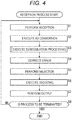
- Fig. 4 is a flowchart illustrating a reception process. Note that an exemplary case of receiving a signal from the satellite 5 will be described in the following descriptions.
- step S1 the tuner 21 receives the signal transmitted via the satellite 5, and outputs a baseband signal including the I signal and the Q signal.
- step S2 the ADC 51 carries out the AD conversion of the input I signal and the Q signal.
- step S3 the satellite demodulation unit 71 executes demodulation processing.
- the I signal and the Q signal are subject to frequency synchronization and phase synchronization.
- the I signal and the Q signal are orthogonally demodulated.
- step S4 the error correction unit 74 performs error correction on the signal using the LDPC/BCH decoder 81 and the Viterbi/RS decoder 82.
- step S5 in a case where reception of a satellite broadcast is indicated on the basis of an instruction from the user, the output control unit 76 selects the signal demodulated by the satellite demodulation unit 71.
- step S6 the decoder 23 decodes the video signal and the audio signal of the signal input from the output control unit 76.
- step S7 the monitor 24 outputs an image corresponding to the signal supplied from the decoder 23 on a display to perform display and output a sound from a speaker.
- step S8 it is determined whether or not to terminate the process on the basis of an instruction from the user, and in a case where a termination of the process is not instructed, the process returns to step S1 and the subsequent processing is repeated. In a case where the termination of the process is instructed, the process is terminated.
- Fig. 5 is a block diagram illustrating a configuration of the satellite demodulation unit according to the present technology.
- a multiplier 201 performs frequency detection on a carrier wave input from the ADC 51 by multiplying an oscillation signal having a predetermined frequency oscillated and output by a numerical controlled oscillator (NCO) 213 of a frequency synchronization unit 206.
- NCO numerical controlled oscillator
- a timing synchronization unit 202 adjusts a timing of a detection signal.
- a phase of a clock for sampling input from the PLL 53 to the ADC 51 is influenced by a state of the external environment, and is not necessarily stable. Therefore, the timing is adjusted so that the signal can be demodulated without excess or deficiency.
- a matched filter 203 is a bandpass filter, which allows only a signal having a predetermined frequency band to pass to maximize an SN.
- the matched filter 203 is configured as illustrated in Fig. 6 , for example.
- Fig. 6 is a block diagram illustrating a configuration of the matched filter according to the present technology.
- the matched filter 203 includes a finite impulse response (FIR) filter.
- FIR finite impulse response
- An input signal is sequentially delayed by one clock by a delay unit 251 1 to a delay unit 251 N-1 , and is output to the subsequent stage.
- a multiplier 252 0 multiplies the input I signal or the Q signal by a coefficient C 0 .
- Multipliers 252 1 to 252 N-1 multiply the I signals output from the corresponding delay units 251 1 to 251 N-1 by coefficients C 1 to C N-1 .
- An output from each multiplier 252 I is added by an adder 253.
- a roll-off rate of the matched filter 203 is required to be 0.03. Accordingly, the number of taps increases. However, in the case of the present embodiment, the number of taps of the matched filter 203 is not increased as much as the case of the roll-off rate of 0.03. In other words, it includes a smaller number of taps. As a result, the frequency band to be passed through cannot be made sufficiently narrow, and intersymbol interference occurs in an unchanged condition, whereby the roll-off rate of 0.03 cannot be eventually achieved. Therefore, in the present embodiment, a frequency estimation unit 212 performs control to limit the influence exerted by the intersymbol interference, thereby eventually achieving a function equivalent to the case of the roll-off rate of 0.03.
- An equalizer 204 in Fig. 5 adjusts the signals such that a frequency response becomes equal at each frequency.
- a phase synchronization unit 205 includes a PLL, and synchronizes a phase of the carrier wave of the reception signal input to the multiplier 201 with a phase of the oscillation signal output from the NCO 213 to the multiplier 201.
- the frequency synchronization unit 206 performs adjustment such that the frequency of the carrier wave of the reception signal input to the multiplier 201 is synchronized with the frequency of the oscillation signal output from the NCO 213 to the multiplier 201. Accordingly, a frame synchronization unit 211 detects the head position of the synchronization signal. For example, each square sum of a synchronous detection value of the I signal (result of correlation with FSync, SSync, and !FSync) and a synchronous detection value of the Q signal (result of correlation with FSync, SSync, and !FSync) is calculated. A position in which a value of the square sum is the largest is set to be the head position of the modulation slot. The frequency is detected using an angle of the symbol on the complex plane of the synchronous detection value (i.e., represented by coordinates (synchronous detection value of I signal and synchronous detection value of Q signal)).
- the frequency estimation unit 212 detects a phase difference between the symbols of the synchronization signal by operation correlation, and estimates a frequency error on the basis of the detected phase difference.
- the NCO 213 generates a signal having a frequency corresponding to the frequency error estimated by the frequency estimation unit 212, and outputs it to the multiplier 201.
- a coarse adjustment is performed such that the frequencies of the carrier wave of the reception signal and the oscillation signal output from the NCO 213 to the multiplier 201 are synchronized by the loop including the frequency synchronization unit 206, and a fine adjustment is performed such that the phases are synchronized by the phase synchronization unit 205.
- a signal having been subject to the phase synchronization by the phase synchronization unit 205 is output to the subsequent stage (not illustrated), and is orthogonally demodulated.
- Fig. 7 is a flowchart illustrating a synchronization process.
- step S11 the multiplier 201 multiplies a carrier wave signal of the reception signal by the oscillation signal adjusted to have a predetermined frequency generated by the NCO 213, and detects the carrier wave.
- step S12 the timing synchronization unit 202 synchronizes the timing of the detection signal.
- the timing of the signal output is adjusted such that the reception signal can be demodulated without excess or deficiency even in a case where the phase of the clock for sampling input from the PLL 53 to the ADC 51 in Fig. 2 is influenced by a state of the external environment and is unstable.
- step S13 the matched filter 203 limits the frequency band of the reception signal in which the timing is adjusted, and allows only the signal having the predetermined frequency band to pass.
- step S14 the equalizer 204 equalizes the signals with limited frequency band such that the frequency response becomes equal at each frequency.
- step S15 the phase synchronization unit 205 including the PLL synchronizes the phase of the carrier wave of the reception signal input to the multiplier 201 with the phase of the oscillation signal output from the NCO 213 to the multiplier 201, is output to the subsequent stage, and performs orthogonal detection.
- step S16 the frame synchronization unit 211 of the frequency synchronization unit 206 detects the head position of the synchronization signal. In other words, the head position of the FSync, SSync, and !FSync is detected.
- the frequency estimation unit 212 estimates the frequency error on the basis of differential correlation.
- the frequency error is estimated on the basis of the phase difference between the symbols of the synchronization signal including 24 symbols starting from the head position detected by the frame synchronization unit 211, and a control signal having a value corresponding to the error is generated.
- the influence exerted by the intersymbol interference is controlled to be reduced in estimating the frequency error. Accordingly, even in a case where the number of taps of the matched filter 203 is reduced, the SN similar to the number of taps of the case where the roll-off rate is set to 0.03 can be achieved.
- step S18 the NCO 213 generates the oscillation signal having the frequency corresponding to the frequency error on the basis of the control signal supplied from the frequency estimation unit 212.
- the oscillation signal is output to the multiplier 201.
- step S19 the multiplier 201 determines whether or not to terminate the process on the basis of an instruction from the user. In a case where a termination of the process is not instructed, the process returns to step S11 and the subsequent processing is repeated.
- control is performed such that the error between the frequency of the carrier wave of the reception signal input to the multiplier 201 and the frequency of the oscillation signal output from the NCO 213 to the multiplier 201 becomes small (coarse adjustment of initial demodulation is performed) and also that the phase difference therebetween becomes small (finely adjusted).
- the adjustment is performed in the order of the timing adjustment by the timing synchronization unit 202, the frequency synchronization by the frequency synchronization unit 206, and the phase synchronization by the phase synchronization unit 205.
- Fig. 8 is a diagram illustrating the phase difference between the symbols.
- a signal point on the complex plane represented by an I axis and a Q axis in each of the 24 symbols (Sync sequence) included in the synchronization signal is as illustrated in the upper part in Fig. 8 .
- the phase difference between adjacent symbols advances or delays by 90 degrees such as the upper right (first quadrant) in a first symbol, the upper left (second quadrant) in a second symbol, the lower left (third quadrant) in a third symbol, the upper left (second quadrant) in a fourth symbol, ..., and the lower right (fourth quadrant) in a 24th symbol.
- the phase difference between the adjacent symbols after the modulation of the synchronization signal is released is as illustrated in the lower part in Fig. 8 .
- the signal point is the upper right (first quadrant) in the first symbol, the upper left (second quadrant) in the second symbol, the upper right (first quadrant) in the third symbol, ..., and the upper left (second quadrant) in the 24th symbol. Therefore, the phase difference between the first symbol and the second symbol is +90 degrees, the phase difference between the second symbol and the third symbol is -90 degrees, the phase difference between the third symbol and the fourth symbol is +90 degrees, and so on, and the phase difference of +90 degrees and -90 degrees alternately appears.
- Fig. 9 is a diagram illustrating the phase difference between the symbols in a case where there is a frequency error.
- the upper part in Fig. 9 illustrates a state before the modulation is released.
- the position of the signal point in Fig. 9 is slightly shifted from the position of the signal point in Fig. 9 . That is, the phase is shifted.
- the lower part in Fig. 9 illustrates a state after the modulation is released.
- the phase advances by an angle ⁇ from the phase of a case where there is no frequency error (phase in the lower part in Fig. 8 ).
- the phase advances by an angle 2 ⁇ from the phase of the case where there is no frequency error (phase in the lower part in Fig. 8 )
- the phase advances by an angle 3 ⁇ from the phase of the case where there is no frequency error (phase in the lower part in Fig. 8 ).
- the phase advances by an angle 23 ⁇ from the phase of the case where there is no frequency error (phase in the lower part in Fig. 8 ).
- the phase difference between the first symbol and the second symbol is +(90 degrees + ⁇ )
- the phase difference between the second symbol and the third symbol is -(90 degrees + ⁇ )
- the phase difference between the third symbol and the fourth symbol is +(90 degrees + ⁇ ).
- +(90 degrees + ⁇ ) and -(90 degrees + ⁇ ) alternately appear as the phase difference. Therefore, the frequency error can be detected by detecting this deviation angle ⁇ .
- a frequency error ⁇ f can be obtained from the deviation angle ⁇ on the basis of the following formula.
- ⁇ ⁇ f ⁇ / 360 ⁇ 33.7561
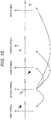
- Fig. 10 is a diagram illustrating the intersymbol interference.
- the intersymbol interference indicates that a signal of one symbol leaks into a signal of another symbol.
- Fig. 10 illustrates a state in which no frequency error exists and the signal of the second symbol leaks into the other first symbol, third symbol, fourth symbol, ..., and 24th symbol.
- Leakage can be represented by a vector.
- a vector indicated by an arrow in the drawing representing the signal point of the second symbol is added to another symbol such as another first symbol, third symbol, fourth symbol, ..., and 24th symbol at a predetermined ratio.
- a leakage amount corresponds to a distance between the symbols, which decreases as the distance increases. In Fig. 10 as well, the longer the distance becomes, the shorter the length of the vector becomes.
- Fig. 11 is a diagram illustrating the influence exerted by the intersymbol interference on the frequency error.
- the upper part in Fig. 11 illustrates a state before the modulation is released in a case where no frequency error exists and the intersymbol interference occurs.
- the lower part in Fig. 11 illustrates a state in which the modulation of the Sync sequence in the upper part in Fig. 11 is released.
- the phase difference between the first symbol and the second symbol is +(90 degrees + X 1 )
- the phase difference between the second symbol and the third symbol is -(90 degrees + X 2 )
- the phase difference between the third symbol and the fourth symbol is +(90 degrees + X 3 )
- the phase difference of +(90 degrees + X n ) and -(90 degrees + X n-1 ) alternately appears.
- the frequency estimation unit 212 is controlled to suppress a component based on the intersymbol interference.
- Fig. 12 is a block diagram illustrating the configuration of the frequency estimation unit according to the present technology.
- a synchronization signal extracting unit 301 extracts a synchronization signal from the signal supplied from the frame synchronization unit 211.
- a synchronization signal demodulation unit 302 demodulates the synchronization signal extracted by the synchronization signal extracting unit 301.
- a phase difference detection unit 303 detects a phase difference from the synchronization signal demodulated by the synchronization signal demodulation unit 302. As a result, the component based on the intersymbol interference is controlled.
- a 90-degree correction unit 304 corrects 90 degrees out of the phase differences detected by the phase difference detection unit 303.
- a symbol averaging unit 305 calculates an average value of the phase difference between the symbols from the output of the 90-degree correction unit 304.
- a conversion unit 306 converts the average value calculated by the symbol averaging unit 305 into a corresponding frequency error. In other words, an estimation value corresponding to the estimated frequency error is output.
- Fig. 13 is a flowchart illustrating a frequency error estimation process according to the present technology.
- the synchronization signal extracting unit 301 extracts the synchronization signal. In other words, from the head position of the synchronization signal detected by the frame synchronization unit 211 serving as a reference, 24 symbols of the FSync, SSync, and !FSync are extracted.
- step S52 the synchronization signal demodulation unit 302 demodulates the synchronization signal.
- the synchronization signal having been subject to ⁇ /2 shift BPSK modulation is demodulated.
- step S53 the phase difference detection unit 303 detects the phase difference of the synchronization signal. This method of detecting the phase difference will be described with reference to Fig. 14 .
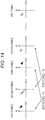
- Fig. 14 is a diagram illustrating the detection of the phase difference between the symbols.
- Fig. 14 illustrates a state after the modulation is released in a case where no frequency error exists.
- a phase difference between the symbols two-symbol away from each other (distance K between symbols (to be described later with reference to Formula 3) is two), not the adjacent symbols, is detected.
- the phase difference (zero degree + Y 1 ) between the first symbol and the third symbol, the phase difference (zero degree + Y 2 ) between the second symbol and the fourth symbol, ..., and the phase difference (zero degree + Y 22 ) (not illustrated) between the 22th symbol and the 24th symbol are detected, respectively.
- the phase difference between the symbols two-symbol away from each other (distance K between symbols is two) is detected. However, it may be a phase difference between the symbols three or more symbols away from each other (distance K between symbols is three or more).
- K represents the distance between the separated symbols.
- K 2.
- the formula (3) is the same as the formula (2).
- ⁇ is an angle (deviation angle) corresponding to the frequency error.
- the angle is estimated with a deviation amount from zero degree, and in the case of an odd number, the angle is estimated from a deviation amount from 90 degrees.
- the 90-degree correction unit 304 corrects 90 degrees from the detected phase. That is, as illustrated in Fig. 11 , in a case where the component of 90 degrees such as (90 degrees + X i ) and -(90 degrees + X i+1 ) appears in the phase difference between the symbols, control (removal) is performed such that the value does not affect the average value of the phase difference. However, in the in the exemplary case in Fig. 14 , since the value to appear is zero degree, substantially no processing is performed in the 90-degree correction unit 304, and the signal is output as it is.
- step S56 the conversion unit 306 converts the phase difference into the corresponding frequency.
- the frequency error ⁇ f is calculated according to the formula (3).
- the NCO 213 in Fig. 5 to which the frequency error ⁇ f is input generates an oscillation signal having the frequency corresponding to the frequency error ⁇ f, and supplies it to the multiplier 201. In this manner, the frequency of the oscillation signal is controlled for each modulation slot to be synchronized with the synchronization signal arranged at the beginning of each modulation slot.
- the oscillation frequency can be controlled by a value obtained by adding the frequency error to a predetermined reference value.
- step S57 the synchronization signal extracting unit 301 determines whether or not to terminate the process on the basis of an instruction from the user. In a case where a termination of the process is not instructed from the user, the process returns to step S51 and the subsequent processing is repeated. In a case where the termination of the process is instructed, the process is terminated.
- the phase difference between the symbols of the distance K 2 to reduce the influence exerted by the intersymbol interference.
- the phase difference between the symbols may be detected by selecting only an optional predetermined one of the 24 symbols.
- a configuration of the frequency estimation unit 212 in this case is similar to the case illustrated in Fig. 12 .
- the phase difference detection unit 303 selects a symbol for detecting the phase difference. In this case, a symbol in which the average value of the component of the intersymbol interference is minimized is selected.
- a component generated by the intersymbol interference (e.g., value X i in Fig. 11 in the case of the phase difference between the adjacent symbols) is dependent on an intersymbol interference amount (leakage amount) and a synchronization signal pattern (i.e., pattern of FSync, SSync, and !FSync).
- the intersymbol interference amount (leakage amount) is determined if a configuration of the matched filter 203 is determined, and the patterns of the FSync, SSync, and !FSync are determined in advance by standards.
- Fig. 15 is a diagram illustrating the detection of the phase difference between the symbols.
- the first symbol, the second symbol, the third symbol, the fourth symbol, ..., the ninth symbol, the 10th symbol, the 11th symbol, and the like are selected.
- phase difference detection unit 303 in Fig. 12 step S53 in Fig. 13
- the phase difference between the selected symbols is detected, and in the symbol averaging unit 305 (step S55), the average value of the phase difference between the selected symbols is calculated. Since it is the phase difference between the selected symbols, this average value contains no or very little intersymbol interference component.
- Other processing is similar to those illustrated in Fig. 13 , and descriptions thereof will be omitted.
- the phase difference between the symbols two or more symbols away from each other is detected in the exemplary case in Fig. 14 , and an optional symbol for detecting the phase difference is selected in the exemplary case in Fig. 15 , thereby reducing the influence exerted by the intersymbol interference.
- the frequency estimation unit 212 can be configured as illustrated in Fig. 16 to reduce the influence exerted by the intersymbol interference.
- Fig. 16 is a block diagram illustrating the configuration of the frequency estimation unit according to the present technology. As is apparent from comparing Fig. 16 with Fig. 12 , the frequency estimation unit 212 in Fig. 16 is different from the frequency estimation unit 212 in Fig. 12 in that a subtractor 321 is disposed between the symbol averaging unit 305 and the conversion unit 306. Other configurations are similar to those of the frequency estimation unit 212 in Fig. 12 , and descriptions thereof will be omitted.
- the subtractor 321 stores a predetermined value in advance, subtracts the stored value from the average value calculated by the symbol averaging unit 305, and outputs it to the conversion unit 306.
- This stored value is set to a value corresponding to the average value of the component (value X i ) generated by the intersymbol interference.
- Fig. 17 is a diagram illustrating the phase difference between the symbols.
- Fig. 17 illustrates a state after the modulation is released in a case where no frequency error exists.
- the phase difference between the two symbols in the case where no frequency error exists is (90 degrees + X 1 ) between the first symbol and the second symbol, -(90 degrees + X 2 ) between the second symbol and the third symbol, (90 degrees + X 3 ) between the third symbol and the fourth symbol, and so on.
- the component (value X i ) generated by the intersymbol interference is dependent on the intersymbol interference amount (leakage amount) and the synchronization signal pattern (i.e., pattern of FSync, SSync, and !FSync). Accordingly, in a case where the phase difference detection unit 303 detects the phase difference between the adjacent symbols, the average value of the values X 1 , X 2 , X 3 , ..., and X 23 in Fig. 17 , that is, the average value of the intersymbol interference component, is set to be the stored value. This average value can be obtained by calculation, experiment, and the like.
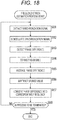
- Fig. 18 is a flowchart illustrating the frequency error estimation process according to the present technology.
- the process in Fig. 18 is a process basically similar to the process in Fig. 13 .
- processing in steps S81 to S85 in Fig. 18 is processing similar to the processing in steps S51 to S55 in Fig. 13
- processing in steps S87 and S88 is processing similar to the processing in steps S56 and S57.
- the process in Fig. 18 is different from the process in Fig. 13 in that processing of step S86 is inserted between steps S85 and S87.
- steps S81 to S85 in Fig. 18 similar to steps S51 to S55 in Fig. 13 is executed by the synchronization extraction unit 301 to the symbol averaging unit 305 in Fig. 16 .
- step S83 the phase difference detection unit 303 detects the phase difference of a case where the distance K between the symbols is minimized to one. Therefore, as is apparent from the formula (3) mentioned above, the width of the frequency error ⁇ f can be increased compared with a case where a value of the distance K is set to two or more.
- the phase difference between the detected symbols is expressed by the following formula. Note that ⁇ is the deviation angle corresponding to the frequency error, and X i is the intersymbol interference component. 90 degrees + ⁇ + X i or ⁇ 90 degrees + ⁇ + X i
- the average value calculated by the symbol averaging unit 305 in step S85 which is the average value of the value obtained by correcting the component of 90 degrees with the 90-degree correction unit 304 in step S84, is expressed by the following expression.
- Av(X i ) is an average value of the intersymbol interference component. ⁇ + Av X i
- the average value of the intersymbol interference component is stored in the subtractor 321 in advance, and in step S86, the subtractor 321 subtracts this stored value from the average value of the phase difference. That is, the average value Av(X i ) of the intersymbol interference component is subtracted from the expression (6), whereby only the deviation angle ⁇ is converted into the frequency error ⁇ f by the conversion unit 306 in step S87.
- Fig. 19 is a chart illustrating the influence exerted by a tap.
- the horizontal axis represents the number of taps of the matched filter 203
- the vertical axis represents a signal power to interference power ratio (SN).
- a curve L 1 represents the characteristic of the current BS/110-degree CS digital broadcasting standard (ISDB-S) with a roll-off rate of 0.35 and a transmission rate of 52 Mbps.
- a curve L 2 represents the characteristic of the ISDB-S3 with a roll-off rate of 0.03 and a maximum bit rate of 142 Mbps, which efficiently transmits higher quality images, voice, and data.
- the SN value is about 46, and if the number of taps is 60, the SN value is about 77.
- the SN value is about 23, and if the number of taps is 60, the SN value is about 47.
- the SN value (about 47) achieved in the case where the number of taps is set to 60 in the curve L 2 (ISDB-S3) is approximately equal to the SN value (about 46) achieved in the case where the number of taps is set to 10 in the curve L 1 (ISDB-S).
- the SN decreases as the number of taps decreases. Furthermore, it is understood that the SN in the curve L 2 is worse overall than in the curve L 1 . In other words, it is understood that the ISDB-S3 requires to minimize deterioration of the SN compared with the ISDB-S (better to increase the number of taps). In the present embodiment, although the number of taps is reduced, the intersymbol interference component is suppressed, whereby the SN similar to that in the case where the number of taps is large can be achieved from the viewpoint of performance.
- the I signal and the Q signal are supplied from the tuner 21 to the demodulating apparatus 22 as separate codes.
- An I signal output terminal of the tuner 21 may be erroneously or intentionally connected to a Q signal input terminal of the demodulating apparatus 22 at times, and a Q signal output terminal of the tuner 21 may be connected to an I signal input terminal of the demodulating apparatus 22 at times.
- a case where intentionally done is, for example, the case where a preferable characteristic can be obtained by employing such a connection in which a difference in length between the two connection codes is made small.
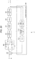
- Fig. 20 is a block diagram illustrating the configuration of the satellite demodulation unit according to the present technology.
- a switching unit 401 is inserted between the multiplier 201 and the timing synchronization unit 202.
- the other configurations are similar to those of the satellite demodulation unit 71 in Fig. 5 .
- the switching unit 401 performs switching such that the I signal output from the multiplier 201 is switched to either the I signal input terminal or the Q signal input terminal of the timing synchronization unit 202 to be input. Likewise, the switching unit 401 performs switching such that the Q signal output from the multiplier 201 is switched to either the Q signal input terminal or the I signal input terminal of the timing synchronization unit 202 to be input. The switching is performed on the basis of a switching signal from the frequency estimation unit 212.
- Fig. 21 is a flowchart illustrating the synchronization process.
- the process in Fig. 21 is basically similar to the process in Fig. 7 .
- processing in step S101 in Fig. 21 is processing similar to the processing in step S11 in Fig. 7
- processing in steps S103 to S110 in Fig. 21 is processing similar to the processing in steps S12 to S19 in Fig. 7 .
- the process in Fig. 21 is different from the process in Fig. 7 in that processing of step S102 is inserted between steps S101 and S103.
- step S102 the switching unit 401 performs switching in accordance with the switching signal.
- the switching signal is supplied from the frequency estimation unit 212.
- the switching unit 401 switches a supply destination of the I signal and the Q signal.
- the I signal output from the multiplier 201 is supplied to the Q signal input terminal of the timing synchronization unit 202, and the Q signal is supplied to the I signal input terminal of the timing synchronization unit 202.
- the switching unit 401 does not switch the supply destination of the I signal and the Q signal.
- the I signal and the Q signal are supplied to the I signal input terminal of the timing synchronization unit 202 and the Q signal input terminal of the timing synchronization unit 202, respectively.
- the I signal and the Q signal are correctly input to each unit subsequent to the timing synchronization unit 202, whereby each processing can be correctly performed.
- the switching unit 401 is disposed before the timing synchronization unit 202 in the exemplary case in Fig. 20 , it is only required to be disposed before the phase synchronization unit 205, and may be disposed, for example, before the multiplier 201, before the equalizer 204, and the like.
- Fig. 22 is a block diagram illustrating the configuration of the frequency estimation unit according to the present technology.
- an IQ inversion detection unit 421 is provided in the frequency estimation unit 212 in Fig. 22 .
- the other configurations are similar to those of the frequency estimation unit 212 in Fig. 12 .
- the phase difference detection unit 303 performs phase difference detection in the case where the distance K between the symbols is two or more and is an odd number.
- the IQ inversion detection unit 421 detects the IQ conversion from the output of the phase difference detection unit 303, and outputs a switching signal corresponding to the detection result to the switching unit 401 in Fig. 20 .
- Fig. 23 is a flowchart illustrating the frequency error estimation process according to the present technology.
- the process in Fig. 23 is basically similar to the process in Fig. 13 .
- Processing in steps S121 to S123 in Fig. 23 is similar to the processing in steps S51 to S53 in Fig. 13
- processing in steps S125 to S128 in Fig. 23 is similar to the processing in steps S54 to S57 in Fig. 13 .
- the process in Fig. 23 is different from the process in Fig. 13 in that processing of step S124 is inserted between steps S123 and S125.
- Fig. 24 is a diagram illustrating the inversion of the I signal and the Q signal.
- Fig. 24 illustrates an exemplary case where the distance K between the symbols is three.
- the upper part in Fig. 24 illustrates the signal in the case where the I signal and the Q signal are not inverted, and the lower part illustrates the signal in the case of being inverted.
- the symbol of the imaginary part (coordinate of Q axis) is opposite in polarity to the case of not being inverted. That is, a complex conjugate relationship is established.
- phase difference between the first symbol and the fourth symbol is +90 degrees in the upper part in which the I signal and the Q signal are not inverted
- the phase difference between the first symbol and the fourth symbol is -90 degrees in the lower part in which the I signal and the Q signal are inverted.
- the phase difference between the second symbol and the fifth symbol is -90 degrees in the upper part, it is +90 degrees in the lower part.
- the phase difference between the third symbol and the sixth symbol is +90 degrees in the upper part, it is -90 degrees in the lower part.
- the IQ inversion detection unit 421 detects the inversion of this symbol. That is, the IQ inversion detection unit 421 stores the symbol of the 90-degree component of the phase difference between the respective symbols in the case where the I signal and the Q signal are not inverted, and in a case where the detected symbol is in a reversed state with respect to the stored symbol, it is determined that the I signal and the Q signal are inverted. On the other hand, in a case where the detected symbol is not in a reversed state with respect to the stored symbol, it is determined that the I signal and the Q signal are not inverted. A result of the determination is supplied to the switching unit 401 in Fig. 20 as a switching signal.
- phase difference detection unit 303 detects the phase difference between the symbols in which the distance K is two or more and is an odd number, as is apparent from the exemplary case in Fig. 25 to be described later, a dedicated phase difference detection unit 451 for the IQ conversion detection is not necessarily provided. Therefore, the configuration is simplified and the cost can be reduced.
- the phase difference between the symbols in which the average value of the component based on the intersymbol interference is minimized can be also detected.
- the processing thereof is similar to that in the case described with reference to Fig. 23 .
- the phase difference between the symbols in this case needs to be the phase difference between the symbols in which the distance K at which the IQ inversion can be detected is an odd number.
- Fig. 25 is a block diagram illustrating the configuration of the frequency estimation unit according to the present technology.
- the phase difference detection unit 451 is provided in the preceding stage of the IQ inversion detection unit 421.
- the other configurations are similar to those of the frequency estimation unit 212 in Fig. 22 .
- the phase difference detection unit 303 performs phase difference detection in the case where the distance K between the symbols is an even number of two or more.
- the phase difference detection unit 451 performs the phase difference detection in the case where the distance K between the symbols is an odd number.
- the other configurations are similar to those in the case in Fig. 22 .
- Fig. 26 is a diagram illustrating the inversion of the I signal and the Q signal.
- Fig. 26 illustrates an exemplary case where the distance K between the symbols is two.
- the upper part in Fig. 26 illustrates the signal in the case where the I signal and the Q signal are not inverted, and the lower part illustrates the signal in the case of being inverted.
- the symbol of the imaginary part (coordinate of Q axis) is opposite in polarity to the case of not being inverted. That is, a complex conjugate relationship is established.
- the phase difference between the first symbol and the third symbol is zero degree in the upper part in which the I signal and the Q signal are not inverted, and the phase difference between the first symbol and the third symbol is also zero degree in the lower part in which the I signal and the Q signal are inverted.
- the phase difference between the second symbol and the fourth symbol is zero degree in the upper part, and is also zero degree in the lower part.
- phase difference detection unit 303 in a signal processing path for original frequency error detection, since the phase difference in the case where the distance K between the symbols is two (even number) is detected, IQ inversion cannot be detected. Accordingly, in the frequency estimation unit 212 in Fig. 25 , in addition to the phase difference detection unit 303 for frequency error detection, the phase difference detection unit 451 for IQ inversion detection is provided in the preceding stage of the IQ inversion detection unit 421. Therefore, from the output of the synchronization signal demodulation unit 303, phase difference detection in the case where the distance K between the symbols is an odd number (e.g., case where the distance K between the symbols is three as illustrated in Fig. 24 ) is performed.
- odd number e.g., case where the distance K between the symbols is three as illustrated in Fig. 24
- Fig. 27 is a flowchart illustrating the frequency error estimation process according to the present technology.
- the process in Fig. 27 is a process basically similar to the process in Fig. 23 (i.e., process in Fig. 13 ).
- processing in steps S141 and S142 is processing similar to the processing in steps S121 and S122 in Fig. 23 (processing in steps S51 and S52 in Fig. 13 )
- processing in steps S145 to S149 is processing similar to the processing in step S123 and steps S125 to S128 in Fig. 23 (processing in steps S53 to S57 in Fig. 13 ).
- processing in step S144 in Fig. 27 is processing similar to the processing in step S124 in Fig. 23 .
- a dedicated phase difference detection is performed in step S143 to perform the IQ inversion detection processing in step S144.
- step S141 the synchronization signal extracting unit 301 to the conversion unit 306 perform processing similar to that in the case in Fig. 23 (i.e., processing similar to that in the case in Fig. 13 ).
- step S143 the phase difference detection unit 451 detects the phase difference of the synchronization signal demodulated by the synchronization signal demodulation unit 302 in step S142.
- the IQ inversion detection unit 421 detects the inversion state of the I signal and the Q signal from the phase difference detected by the phase difference detection unit 451 as described with reference to Fig. 24 , and outputs the determination result to the switching unit 421 in Fig. 20 as a switching signal.
- phase difference detection unit 451 in Fig. 25 is dedicated to IQ inversion detection, and is not used for frequency error estimation, whereby it is acceptable if a slight influence of the intersymbol interference is exerted. Accordingly, as illustrated in Fig. 28 , the phase difference in the case where the distance K between the symbols is one may be detected.
- Fig. 28 is a diagram illustrating the inversion of the I signal and the Q signal.
- Fig. 28 illustrates an exemplary case where the distance K between the symbols is one.
- the upper part in Fig. 28 illustrates the signal in the case where the I signal and the Q signal are not inverted, and the lower part illustrates the signal in the case of being inverted.
- the symbol of the imaginary part (coordinate of Q axis) is opposite in polarity to the case of not being inverted. That is, a complex conjugate relationship is established.
- phase difference between the first symbol and the second symbol is +90 degrees in the upper part in which the I signal and the Q signal are not inverted
- the phase difference between the first symbol and the second symbol is -90 degrees in the lower part in which the I signal and the Q signal are inverted.
- the phase difference between the second symbol and the third symbol is -90 degrees in the upper part, it is +90 degrees in the lower part.
- the phase difference between the third symbol and the fourth symbol is +90 degrees in the upper part, it is -90 degrees in the lower part.
- phase difference detection unit 451 the phase difference in the case where the distance K between the symbols is one may be detected. This also similarly applies to the exemplary case in Fig. 31 to be described later.
- phase difference detection unit 303 The phase difference between the symbols in which the distance K is an even number is detected in the phase difference detection unit 303 in Fig. 25 , and the phase difference between the symbols in which the distance K is an odd number is detected in the phase difference detection unit 451.
- the phase difference detection unit 303 the phase difference between the symbols in which the average value of the component based on the intersymbol interference is minimized is detected, and in the phase difference between the symbols, the configuration of the frequency estimation unit 212 is as illustrated in Fig. 25 even in a case where the IQ inversion cannot be detected.
- the processing thereof is similar to that in the case described with reference to Fig. 27 .
- the phase difference detection unit 451 in this case needs to detect the phase difference between the symbols in which the IQ inversion can be detected.
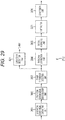
- Fig. 29 is a block diagram illustrating the configuration of the frequency estimation unit according to the present technology.
- the frequency estimation unit 212 in Fig. 29 has a configuration basically similar to that of the frequency estimation unit 212 in Fig. 16 .
- the frequency estimation unit 212 in Fig. 29 is different from the frequency estimation unit 212 in Fig. 16 in that the IQ inversion detection unit 421 is provided.
- Fig. 30 is a flowchart illustrating the frequency error estimation process according to the present technology. Processing in steps S181 to S183 and steps S185 to S189 in Fig. 30 is processing similar to the processing in steps S81 to S88 in Fig. 18 . The process in Fig. 30 is different from the process in Fig. 18 in that processing of step S184 is inserted between steps S183 and S185.
- steps S181 to S183, S185, S186, S188, and S189 processing similar to the processing in steps S81 to S85, S87, and S88 in Fig. 18 , in other words, the processing in steps S51 to S57 in Fig. 13 , is executed.
- step S187 processing of subtracting the stored value similar to the processing in step S86 in Fig. 18 is performed.
- step S184 the IQ inversion detection unit 421 detects the inversion state of the I signal and the Q signal from the phase difference detected by the phase difference detection unit 303 in step S183.
- the detection result is output to the switching unit 401 in Fig. 20 as a switching signal.
- the phase difference detection unit 303 in Fig. 29 the phase difference between the symbols in which the distance K is one may be detected as illustrated in Fig. 28 . This is because the subtractor 321 subtracts the intersymbol interference component with respect to the signal used for the frequency error estimation.
- Fig. 31 is a block diagram illustrating the configuration of the frequency estimation unit according to the present technology.
- the frequency estimation unit 212 in Fig. 31 has a configuration basically similar to that of the frequency estimation unit 212 in Fig. 16 .
- the frequency estimation unit 212 in Fig. 31 is different from the frequency estimation unit 212 in Fig. 16 in that the IQ inversion detection unit 421 is provided and the phase difference detection unit 451 is provided in the preceding stage.
- the other configurations are similar to those in the case in Fig. 16 .
- the frequency estimation unit 212 in Fig. 31 is different from that in Fig. 29 in that the dedicated phase difference detection unit 451 is provided for the IQ inversion detection unit 421 to detect the inversion of the I signal and the Q signal.
- Fig. 32 is a flowchart illustrating the frequency error estimation process according to the present technology. Processing in steps S201, S202, and S205 to S210 in Fig. 32 is processing similar to the processing in steps S81 to S88 in Fig. 18 . The process is different from the process in Fig. 18 in that processing of steps S203 and S204 is inserted between steps S202 and S205.
- processing in steps S201, S202, and steps S205 to S210 in Fig. 32 corresponds to the processing in steps S181 to S183 and S185 to S189 in Fig. 30 .
- the phase difference detection result in step S183 is used to detect the IQ inversion state in step S184.
- a dedicated phase difference detection result for detecting the IQ inversion state in step S203 is used to detect the IQ inversion state in step S204.
- steps S201, S202, S205 to S207, S208, and S210 processing similar to the processing in steps S81 to S85, S87, and S88 in Fig. 18 , in other words, the processing in steps S51 to S57 in Fig. 13 , is executed.
- step S208 processing of subtracting the stored value similar to the processing in step S86 in Fig. 18 is performed.
- step S204 the IQ inversion detection unit 421 detects the inversion state of the I signal and the Q signal on the basis of the phase difference detected by the phase difference detection unit 451. The detection result is output to the switching unit 401 in Fig. 20 as a switching signal.
- embodiments according to the present technology are not limited to the embodiments described above, and various modifications are possible without departing from the gist of the present technology.
- the present technology can also be applied to the case where the roll-off rate is 0.05 or the like.
Landscapes
- Engineering & Computer Science (AREA)
- Computer Networks & Wireless Communication (AREA)
- Signal Processing (AREA)
- Power Engineering (AREA)
- Digital Transmission Methods That Use Modulated Carrier Waves (AREA)
- Circuits Of Receivers In General (AREA)
Abstract
Description
- The present technology relates to a receiving apparatus and method, and a demodulating apparatus, and more particularly, to a receiving apparatus and method and a demodulating apparatus that suppresses influence exerted by intersymbol interference on a frequency error of a synchronization signal.
- Satellite broadcasting has been widespread, and many contents are being broadcast. Along with this, it is desired to broadcast higher definition images in recent years. In order to broadcast high-definition images, it is necessary to synchronize signals at high speed, and various proposals have been made (e.g., Patent Document 1).
- Furthermore, since a data amount becomes large to broadcast high-definition image signals, it is necessary to perform transmission efficiently. Accordingly, it is necessary to transmit signals through a band limiting filter having a small roll-off rate on the transmitting side.
- Patent Document 1: Japanese Patent Application Laid-Open No.
2008-278188 - Basically, a configuration of a receiving apparatus that receives a signal transmitted from the transmitting side needs to correspond to the transmitting side. Therefore, in a case where a filter with a low roll-off rate is used on the transmitting side, it is necessary to use the filter with the same low roll-off rate on the receiving side as well. Specifically, use of a filter with a roll-off rate of 0.03 is expected.
- Meanwhile, in a case where the filter with a low roll-off rate is used, the number of taps of the filter increases, and a circuit scale increases. As a result, a cost increases. Furthermore, a loop delay of a synchronous loop becomes long, and synchronization performance deteriorates. In view of the above, with respect to the receiving apparatus, it is desirable that the number of taps of the filter does not become so large.
- However, if the number of taps of the filter in the receiving apparatus is not sufficient, a component based on intersymbol interference (ISI) with respect to a reception signal cannot be removed. As a result, in a case where a frequency error is detected using a synchronization signal included in a reception signal in the receiving apparatus and a frequency is to be synchronized, deviation (error) based on the intersymbol interference is generated in the detected frequency error, whereby it becomes difficult to accurately synchronize the frequency.
- The present technology has been conceived in view of such a situation, and it is intended to suppress influence exerted by the intersymbol interference on the frequency error of the synchronization signal.
- An aspect of the present technology is a receiving apparatus including an estimation unit that estimates an estimation value of a frequency error of a symbol included in a synchronization signal of a reception signal and a control unit that controls a component based on intersymbol interference of the estimation value.
- The estimation value mentioned above can be estimated from a phase difference between the two symbols.
- A distance between the two symbols may be two or more.
- A detection unit that detects an inversion state of an I signal and a Q signal to be received may be further provided.
- The distance between the two symbols for estimating the estimation value may be an odd number of three or more.
- The estimation value is estimated from the two symbols in which the distance between the symbols is an even number, and the inversion state of the I signal and the Q signal can be detected from the two symbols in which the distance between the symbols is an odd number.
- In a case where the inversion of the I signal and the Q signal to be received is detected, a switching unit that switches the I signal and the Q signal to be processed may be further provided.
- The symbol for detecting the phase difference may be selected for the estimation value so that the component of the intersymbol interference is suppressed.
- The phase difference between the symbols may be averaged to minimize the component of the intersymbol interference.
- The component based on the intersymbol interference of the estimation value can be controlled by subtracting the value corresponding to the component of the intersymbol interference stored in advance.
- The reception signal is detected on the basis of a signal of a frequency controlled in accordance with the estimation value to synchronize the frequency, and a frequency band of the detected signal is limited, whereby the phase of the signal in which the frequency is limited can be synchronized.
- The receiving apparatus can receive advanced broadband satellite broadcasting.
- An aspect of the present technology is a method of reception that includes a step of estimating an estimation value of a frequency error of a symbol included in a synchronization signal of a reception signal and a step of controlling a component based on intersymbol interference of the estimation value.
- An aspect of the present technology is a demodulating apparatus including an estimation unit that estimates an estimation value of a frequency error of a symbol included in a synchronization signal of a reception signal and a control unit that controls a component based on intersymbol interference of the estimation value.
- In an aspect of the present technology, an estimation value of a frequency error of a symbol included in a synchronization signal of a reception signal is estimated, and a component based on intersymbol interference of the estimation value is controlled.
- As described above, according to an aspect of the present technology, influence exerted by intersymbol interference can be suppressed.
- Note that the effects described herein are merely examples and not limited, and additional effects may be included.
-
-
Fig. 1 is a diagram illustrating a configuration of an advanced broadband satellite broadcasting system. -
Fig. 2 is a block diagram illustrating a configuration of a receiving apparatus according to the present technology. -
Fig. 3 is a diagram illustrating a frame configuration of advanced broadband satellite broadcasting. -
Fig. 4 is a flowchart illustrating a reception process. -
Fig. 5 is a block diagram illustrating a configuration of a satellite demodulation unit according to the present technology. -
Fig. 6 is a block diagram illustrating a configuration of a matched filter according to the present technology. -
Fig. 7 is a flowchart illustrating a synchronization process according to the present technology. -
Fig. 8 is a diagram illustrating a phase difference between symbols. -
Fig. 9 is a diagram illustrating a phase difference between symbols in a case where there is a frequency error. -
Fig. 10 is a diagram illustrating intersymbol interference. -
Fig. 11 is a diagram illustrating influence exerted by intersymbol interference on the frequency error. -
Fig. 12 is a block diagram illustrating a configuration of a frequency estimation unit according to the present technology. -
Fig. 13 is a flowchart illustrating a frequency error estimation process according to the present technology. -
Fig. 14 is a diagram illustrating detection of the phase difference between symbols. -
Fig. 15 is another diagram illustrating the detection of the phase difference between symbols. -
Fig. 16 is another block diagram illustrating the configuration of the frequency estimation unit according to the present technology. -
Fig. 17 is another diagram illustrating the phase difference between symbols. -
Fig. 18 is another flowchart illustrating the frequency error estimation process according to the present technology. -
Fig. 19 is a chart illustrating influence exerted by a tap. -
Fig. 20 is another block diagram illustrating the configuration of the satellite demodulation unit according to the present technology. -
Fig. 21 is a flowchart illustrating a synchronization process. -
Fig. 22 is another block diagram illustrating the configuration of the frequency estimation unit according to the present technology. -
Fig. 23 is another flowchart illustrating the frequency error estimation process according to the present technology. -
Fig. 24 is a diagram illustrating an inversion of an I signal and a Q signal. -
Fig. 25 is another block diagram illustrating the configuration of the frequency estimation unit according to the present technology. -
Fig. 26 is another diagram illustrating the inversion of the I signal and the Q signal. -
Fig. 27 is another flowchart illustrating the frequency error estimation process according to the present technology. -
Fig. 28 is another diagram illustrating the inversion of the I signal and the Q signal. -
Fig. 29 is another block diagram illustrating the configuration of the frequency estimation unit according to the present technology. -
Fig. 30 is another flowchart illustrating the frequency error estimation process according to the present technology. -
Fig. 31 is another block diagram illustrating the configuration of the frequency estimation unit according to the present technology. -
Fig. 32 is another flowchart illustrating the frequency error estimation process according to the present technology. - Hereinafter, embodiments for implementing the present technology will be described. Note that descriptions will be given in the following order.
- 1. Advanced Broadband Satellite Broadcasting System (
Figs. 1 to 4 )- (1) Configuration of Advanced Broadband Satellite Broadcasting System (
Fig. 1 ) - (2) Receiving Apparatus (
Fig. 2 ) - (3) Configuration of Frame (
Fig. 3 ) - (4) Operation of Reception (
Fig. 4 )
- (1) Configuration of Advanced Broadband Satellite Broadcasting System (
- 2. First Satellite Demodulation Unit (
Figs. 5 to 19 )- (1) Configuration and Operation of First Satellite Demodulation Unit (
Figs. 5 to 7 ) - (2) Principle of Frequency Error Estimation (
Figs. 8 to 11 ) - (3) First Frequency Estimation Unit (Case where distance K is two or more:
Figs. 12 to 14 ) - (4) Second Frequency Estimation Unit (Case where symbol with minimum ISI average is selected:
Fig. 15 ) - (5) Third Frequency Estimation Unit (Case of ISI subtraction:
Figs. 16 to 18 ) - (6) Influence Exerted by the Number of Taps (
Fig. 19 )
- (1) Configuration and Operation of First Satellite Demodulation Unit (
- 3. Second Satellite Demodulation Unit (Case of IQ inversion detection:
Figs. 20 to 32 )- (1) Configuration and Operation of Second Satellite Demodulation Unit (
Figs. 20 and21 ) - (2) Fourth Frequency Estimation Unit (Case where IQ inversion is detected, and distance K is two or more and odd number:
Figs. 22 to 24 ) - (3) Fifth Frequency Estimation Unit (Case where IQ inversion is detected, symbol with minimum ISI average is selected, and distance K is odd number:
Figs. 15 ,22 , and23 ) - (4) Sixth Frequency Estimation Unit (Case where IQ inversion is detected, and distance K is two or more and even number:
Figs. 25 to 28 ) - (5) Seventh Frequency Estimation Unit (Case where IQ inversion is detected, symbol with minimum ISI average is selected, and distance K is even number:
Figs. 15 ,25 , and27 ) - (6) Eighth Frequency Estimation Unit (Case where IQ inversion is detected, ISI subtraction is performed, and distance K is odd number:
Figs. 29 and30 ) - (7) Ninth Frequency Estimation Unit (Case where IQ inversion is detected, ISI subtraction is performed, and distance K is even number:
Figs. 31 and32 )
- (1) Configuration and Operation of Second Satellite Demodulation Unit (
- 4. Others
-
Fig. 1 is a diagram illustrating a configuration of an advanced broadband satellite broadcasting system. In an advanced broadbandsatellite broadcasting system 1, broadcasters 2-1 to 2-n digitalize content to be broadcast and transmit it to a transmittingapparatus 3. Although the transmittingapparatus 3 is managed by an operator different from the broadcasters 2-1 to 2-n in many cases, it may be the same operator. A plurality of contents from the respective broadcasters 2-1 to 2-n is gathered as necessary, and is transmitted to asatellite 5 via anantenna 4. Thesatellite 5 is a broadcast satellite (BS) or a communication satellite (CS). - Note that, although only one
antenna 4 is illustrated inFig. 1 , a plurality ofantennas 4 of the same or different operator may be provided. - The
satellite 5 applies predetermined processing onto the signal transmitted from theantenna 4 as necessary, and then transmits it to receiving apparatuses 7-1 to 7-m placed in each house or the like. The receiving apparatuses 7-1 to 7-m receive the signal from thesatellite 5 via corresponding antennas 6-1 to 6-m. -
Fig. 2 is a block diagram illustrating a configuration of a receiving apparatus according to the present technology. This receivingapparatus 11 corresponds to each of the receiving apparatuses 7-1 to 7-m inFig. 1 . - The receiving
apparatus 11 includes atuner 21, ademodulating apparatus 22, adecoder 23, and amonitor 24. Thetuner 21 receives the signal from thesatellite 5, and outputs an I signal and a Q signal, which are baseband signals, to thedemodulating apparatus 22. Thetuner 21 has a function of also receiving a terrestrial broadcast signal, and outputs the intermediate frequency (IF) signal. - The
demodulating apparatus 22 is configured by, for example, a large-scale integrated circuit (LSI), and includes an analogfront end 41 and ademodulation block 42. The analogfront end 41 carries out AD conversion of the respective I signal and the Q signal of the baseband signal from thetuner 21 using an analog-to-digital converter (ADC) 51, and outputs them to asatellite demodulation unit 71 of thedemodulation block 42. AnADC 52 of the analogfront end 41 carries out the AD conversion of an IF signal from thetuner 21, and outputs it to a ground-baseddemodulation unit 72 of thedemodulation block 42. - The analog
front end 41 includes a phase locked loop (PLL) 53. ThePLL 53 includes acrystal 54, and generates a clock having a predetermined frequency. The clock generated by thePLL 53 is divided by adivider 55 to have a predetermined frequency, and is supplied to theADCs PLL 53 is supplied to aclock generation unit 56. Theclock generation circuit 56 generates a clock having a predetermined frequency required by each circuit, and supplies it to each circuit. - In the
demodulation block 42, thesatellite demodulation unit 71 orthogonally demodulates the I signal and the Q signal output from theADC 51 of the analogfront end 41, and outputs them to anerror correction unit 74. Furthermore, the ground-baseddemodulation unit 72 demodulates the IF signal output from theADC 52 of the analogfront end 41, and outputs it to theerror correction unit 74. - The
error correction unit 74 includes a low-density parity-check (LDPC)/BCH decoder 81 and a Viterbi/Reed-Solomon (RS)decoder 74, and performs error correction processing on the signal from thesatellite demodulation unit 71 and the ground-baseddemodulation unit 72 to output it to anoutput control unit 76. - Furthermore, in the
demodulation block 42, acable demodulation unit 73 demodulates a cable television signal supplied from theADC 52, and outputs it to theerror correction unit 75. Theerror correction unit 75 including a Reed-Solomon (RS)decoder 91 corrects the demodulated cable television signal, and outputs it to theoutput control unit 76. - The
output control unit 76 selects any one of a satellite broadcast signal, a terrestrial broadcast signal, and the cable television signal on the basis of an instruction from a user, and outputs it to thedecoder 23. Thedecoder 23 decodes a video signal and an audio signal input from theoutput control unit 76, and outputs it to themonitor 24. Themonitor 24 displays an image corresponding to the input signal, and outputs a corresponding sound. -
Fig. 3 is a diagram illustrating a frame configuration of the advanced broadband satellite broadcasting used in the advanced broadbandsatellite broadcasting system 1 inFig. 1 . Specifically, a frame configuration of the integrated services digital broadcasting for satellite 3 (ISDB-S3) method is illustrated. In the ISDB-S3, it is intended to transmit an image having resolution of what is called 4K and 8K. A transmission rate is 33.7561 MSps. A signal is transmitted in frame units, and one frame includes 120 modulation slots (modulation slots # 1 to #120). - At the beginning of each modulation slot, a synchronization signal including 24 symbols is arranged. The synchronization signal is any one of three types of FSync, SSync, and !Sync. A synchronization signal of the
modulation slot # 1 is set to the FSync, and a synchronization signal of themodulation slot # 2 is set to the SSync. In themodulation slot # 3 and subsequent modulation slots, synchronization signals of the !FSync and the SSync are alternately arranged. The !FSync is a synchronization signal obtained by inverting the FSync. - Next to the synchronization signal, a pilot signal (indicated by P in
Fig. 3 ) including 32 symbols is arranged. This is a transmission signal point arrangement signal that indicates an arrangement of a transmission signal point. - Following to this, 66 pairs of data including 136 symbols and a transmission and multiplexing configuration and control (TMCC) signal including four symbols are arranged. Therefore, one modulation slot includes 9,296 symbols, and has a length of 0.285 ms. Furthermore, data of one modulation slot (
data # 1 to data #66) includes 8,976 symbols, and the TMCC signal of one modulation slot includes 264 (= 4 × 66) symbols. In one frame, 7,920 data (data # 1 to data #7,920), each of which includes 136 symbols, is transmitted, and 7,920 TMCC signals, each of which includes four symbols (31,680 symbols = 4 symbols × 7, 920 bursts), are transmitted. The number of symbols per frame is 1,115,520 (= 9,296 × 120). - A plurality of modulation schemes can be mixed within one frame in the advanced broadband satellite broadcasting. For example, a maximum of eight transmission modes can be defined within one frame, and a different modulation scheme can be adopted in an individual transmission mode. As the modulation scheme, any one of five types of modulation schemes, that is, binary phase shift keying (BPSK), quadrature phase shift keying (QPSK), 8PSK, 16 amplitude and phase shift keying (APSK), and 32APSK, can be used. However, the synchronization signal and a transmission TMCC signal are modulated using the π/2 shift BPSK method.
- Next, operation of the receiving
apparatus 11 illustrated inFig. 2 will be described with reference toFig. 4. Fig. 4 is a flowchart illustrating a reception process. Note that an exemplary case of receiving a signal from thesatellite 5 will be described in the following descriptions. - In step S1, the
tuner 21 receives the signal transmitted via thesatellite 5, and outputs a baseband signal including the I signal and the Q signal. In step S2, theADC 51 carries out the AD conversion of the input I signal and the Q signal. - In step S3, the
satellite demodulation unit 71 executes demodulation processing. As will be described later with reference toFig. 7 and the like, the I signal and the Q signal are subject to frequency synchronization and phase synchronization. Then, the I signal and the Q signal are orthogonally demodulated. - In step S4, the
error correction unit 74 performs error correction on the signal using the LDPC/BCH decoder 81 and the Viterbi/RS decoder 82. In step S5, in a case where reception of a satellite broadcast is indicated on the basis of an instruction from the user, theoutput control unit 76 selects the signal demodulated by thesatellite demodulation unit 71. - In step S6, the
decoder 23 decodes the video signal and the audio signal of the signal input from theoutput control unit 76. - In step S7, the
monitor 24 outputs an image corresponding to the signal supplied from thedecoder 23 on a display to perform display and output a sound from a speaker. - In step S8, it is determined whether or not to terminate the process on the basis of an instruction from the user, and in a case where a termination of the process is not instructed, the process returns to step S1 and the subsequent processing is repeated. In a case where the termination of the process is instructed, the process is terminated.
- Next, a configuration of the
satellite demodulation unit 71 inFig. 2 will be described with reference toFig. 5 . Note that a configuration for frequency synchronization and phase synchronization before orthogonal demodulation will be mainly described. -
Fig. 5 is a block diagram illustrating a configuration of the satellite demodulation unit according to the present technology. As illustrated inFig. 5 , in thesatellite demodulation unit 71, amultiplier 201 performs frequency detection on a carrier wave input from theADC 51 by multiplying an oscillation signal having a predetermined frequency oscillated and output by a numerical controlled oscillator (NCO) 213 of afrequency synchronization unit 206. Atiming synchronization unit 202 adjusts a timing of a detection signal. In other words, a phase of a clock for sampling input from thePLL 53 to theADC 51 is influenced by a state of the external environment, and is not necessarily stable. Therefore, the timing is adjusted so that the signal can be demodulated without excess or deficiency. - A matched
filter 203 is a bandpass filter, which allows only a signal having a predetermined frequency band to pass to maximize an SN. The matchedfilter 203 is configured as illustrated inFig. 6 , for example.Fig. 6 is a block diagram illustrating a configuration of the matched filter according to the present technology. As illustrated inFig. 6 , the matchedfilter 203 includes a finite impulse response (FIR) filter. - An input signal is sequentially delayed by one clock by a delay unit 2511 to a delay unit 251N-1, and is output to the subsequent stage. A multiplier 2520 multiplies the input I signal or the Q signal by a coefficient C0. Multipliers 2521 to 252N-1 multiply the I signals output from the corresponding delay units 2511 to 251N-1 by coefficients C1 to CN-1. An output from each multiplier 252I is added by an
adder 253. One delay unit 251i (i = 1, 2, ..., N-1) and one multiplier 252i (i = 1, 2, ..., N-1) form a tap. - Setting a value of the input signal to be x[n], an output y[n] if the
adder 253 is expressed by the following formula.
- In the advanced broadband satellite broadcasting, a roll-off rate of the matched
filter 203 is required to be 0.03. Accordingly, the number of taps increases. However, in the case of the present embodiment, the number of taps of the matchedfilter 203 is not increased as much as the case of the roll-off rate of 0.03. In other words, it includes a smaller number of taps. As a result, the frequency band to be passed through cannot be made sufficiently narrow, and intersymbol interference occurs in an unchanged condition, whereby the roll-off rate of 0.03 cannot be eventually achieved. Therefore, in the present embodiment, afrequency estimation unit 212 performs control to limit the influence exerted by the intersymbol interference, thereby eventually achieving a function equivalent to the case of the roll-off rate of 0.03. - An
equalizer 204 inFig. 5 adjusts the signals such that a frequency response becomes equal at each frequency. Aphase synchronization unit 205 includes a PLL, and synchronizes a phase of the carrier wave of the reception signal input to themultiplier 201 with a phase of the oscillation signal output from theNCO 213 to themultiplier 201. - The
frequency synchronization unit 206 performs adjustment such that the frequency of the carrier wave of the reception signal input to themultiplier 201 is synchronized with the frequency of the oscillation signal output from theNCO 213 to themultiplier 201. Accordingly, aframe synchronization unit 211 detects the head position of the synchronization signal. For example, each square sum of a synchronous detection value of the I signal (result of correlation with FSync, SSync, and !FSync) and a synchronous detection value of the Q signal (result of correlation with FSync, SSync, and !FSync) is calculated. A position in which a value of the square sum is the largest is set to be the head position of the modulation slot. The frequency is detected using an angle of the symbol on the complex plane of the synchronous detection value (i.e., represented by coordinates (synchronous detection value of I signal and synchronous detection value of Q signal)). - The
frequency estimation unit 212 detects a phase difference between the symbols of the synchronization signal by operation correlation, and estimates a frequency error on the basis of the detected phase difference. TheNCO 213 generates a signal having a frequency corresponding to the frequency error estimated by thefrequency estimation unit 212, and outputs it to themultiplier 201. - A coarse adjustment is performed such that the frequencies of the carrier wave of the reception signal and the oscillation signal output from the
NCO 213 to themultiplier 201 are synchronized by the loop including thefrequency synchronization unit 206, and a fine adjustment is performed such that the phases are synchronized by thephase synchronization unit 205. A signal having been subject to the phase synchronization by thephase synchronization unit 205 is output to the subsequent stage (not illustrated), and is orthogonally demodulated. - Next, synchronous operation of the
satellite demodulation unit 71 inFig. 5 will be described with reference toFig. 7. Fig. 7 is a flowchart illustrating a synchronization process. - In step S11, the
multiplier 201 multiplies a carrier wave signal of the reception signal by the oscillation signal adjusted to have a predetermined frequency generated by theNCO 213, and detects the carrier wave. - In step S12, the
timing synchronization unit 202 synchronizes the timing of the detection signal. In other words, the timing of the signal output is adjusted such that the reception signal can be demodulated without excess or deficiency even in a case where the phase of the clock for sampling input from thePLL 53 to theADC 51 inFig. 2 is influenced by a state of the external environment and is unstable. - In step S13, the matched
filter 203 limits the frequency band of the reception signal in which the timing is adjusted, and allows only the signal having the predetermined frequency band to pass. - In step S14, the
equalizer 204 equalizes the signals with limited frequency band such that the frequency response becomes equal at each frequency. - In step S15, the
phase synchronization unit 205 including the PLL synchronizes the phase of the carrier wave of the reception signal input to themultiplier 201 with the phase of the oscillation signal output from theNCO 213 to themultiplier 201, is output to the subsequent stage, and performs orthogonal detection. - In step S16, the
frame synchronization unit 211 of thefrequency synchronization unit 206 detects the head position of the synchronization signal. In other words, the head position of the FSync, SSync, and !FSync is detected. - The
frequency estimation unit 212 estimates the frequency error on the basis of differential correlation. In other words, the frequency error is estimated on the basis of the phase difference between the symbols of the synchronization signal including 24 symbols starting from the head position detected by theframe synchronization unit 211, and a control signal having a value corresponding to the error is generated. In the case of the present embodiment, the influence exerted by the intersymbol interference is controlled to be reduced in estimating the frequency error. Accordingly, even in a case where the number of taps of the matchedfilter 203 is reduced, the SN similar to the number of taps of the case where the roll-off rate is set to 0.03 can be achieved. - In step S18, the
NCO 213 generates the oscillation signal having the frequency corresponding to the frequency error on the basis of the control signal supplied from thefrequency estimation unit 212. The oscillation signal is output to themultiplier 201. - In step S19, the
multiplier 201 determines whether or not to terminate the process on the basis of an instruction from the user. In a case where a termination of the process is not instructed, the process returns to step S11 and the subsequent processing is repeated. - By the process described above being repeated, control is performed such that the error between the frequency of the carrier wave of the reception signal input to the
multiplier 201 and the frequency of the oscillation signal output from theNCO 213 to themultiplier 201 becomes small (coarse adjustment of initial demodulation is performed) and also that the phase difference therebetween becomes small (finely adjusted). - Note that, although the operation has been described according to each block in
Fig. 5 in the above descriptions, in practice, the adjustment is performed in the order of the timing adjustment by thetiming synchronization unit 202, the frequency synchronization by thefrequency synchronization unit 206, and the phase synchronization by thephase synchronization unit 205. - Next, a principle of frequency error estimation performed in step S17 in
Fig. 7 by thefrequency estimation unit 212 inFig. 5 will be described.Fig. 8 is a diagram illustrating the phase difference between the symbols. In an ideal case where no frequency error exists in the carrier wave and the oscillation signal, a signal point on the complex plane (signal point constellation diagram) represented by an I axis and a Q axis in each of the 24 symbols (Sync sequence) included in the synchronization signal is as illustrated in the upper part inFig. 8 . In other words, with respect to the signal point on the complex plane, the phase difference between adjacent symbols advances or delays by 90 degrees such as the upper right (first quadrant) in a first symbol, the upper left (second quadrant) in a second symbol, the lower left (third quadrant) in a third symbol, the upper left (second quadrant) in a fourth symbol, ..., and the lower right (fourth quadrant) in a 24th symbol. - Therefore, the phase difference between the adjacent symbols after the modulation of the synchronization signal is released is as illustrated in the lower part in
Fig. 8 . In other words, the signal point is the upper right (first quadrant) in the first symbol, the upper left (second quadrant) in the second symbol, the upper right (first quadrant) in the third symbol, ..., and the upper left (second quadrant) in the 24th symbol. Therefore, the phase difference between the first symbol and the second symbol is +90 degrees, the phase difference between the second symbol and the third symbol is -90 degrees, the phase difference between the third symbol and the fourth symbol is +90 degrees, and so on, and the phase difference of +90 degrees and -90 degrees alternately appears. - Meanwhile, in a case where there is a frequency error in the carrier wave and the oscillation signal, it is as follows.
Fig. 9 is a diagram illustrating the phase difference between the symbols in a case where there is a frequency error. The upper part inFig. 9 illustrates a state before the modulation is released. As is apparent from comparing the upper part inFig. 9 with the upper part inFig. 8 , the position of the signal point inFig. 9 is slightly shifted from the position of the signal point inFig. 9 . That is, the phase is shifted. - The lower part in
Fig. 9 illustrates a state after the modulation is released. In the second symbol, the phase advances by an angle θ from the phase of a case where there is no frequency error (phase in the lower part inFig. 8 ). In the third symbol, the phase advances by an angle 2θ from the phase of the case where there is no frequency error (phase in the lower part inFig. 8 ), and in the fourth symbol, the phase advances by an angle 3θ from the phase of the case where there is no frequency error (phase in the lower part inFig. 8 ). Further, in the 24th symbol, the phase advances by an angle 23θ from the phase of the case where there is no frequency error (phase in the lower part inFig. 8 ). - Therefore, the phase difference between the first symbol and the second symbol is +(90 degrees + θ), the phase difference between the second symbol and the third symbol is -(90 degrees + θ), and the phase difference between the third symbol and the fourth symbol is +(90 degrees + θ). Likewise, +(90 degrees + θ) and -(90 degrees + θ) alternately appear as the phase difference. Therefore, the frequency error can be detected by detecting this deviation angle θ.
- In other words, a frequency error Δf can be obtained from the deviation angle θ on the basis of the following formula.

- Note that 33.7561 (MHz) is a symbol rate.
- Next, the intersymbol interference will be described.
Fig. 10 is a diagram illustrating the intersymbol interference. The intersymbol interference indicates that a signal of one symbol leaks into a signal of another symbol.Fig. 10 illustrates a state in which no frequency error exists and the signal of the second symbol leaks into the other first symbol, third symbol, fourth symbol, ..., and 24th symbol. - Leakage can be represented by a vector. In other words, a vector indicated by an arrow in the drawing representing the signal point of the second symbol is added to another symbol such as another first symbol, third symbol, fourth symbol, ..., and 24th symbol at a predetermined ratio. A leakage amount corresponds to a distance between the symbols, which decreases as the distance increases. In
Fig. 10 as well, the longer the distance becomes, the shorter the length of the vector becomes. - Note that, although the leakage of the second symbol into another symbol is illustrated in
Fig. 10 , the symbols other than the second symbol also leak into other symbols in a similar manner. - In a case where such intersymbol interference occurs, it is erroneously detected as a frequency error.
Fig. 11 is a diagram illustrating the influence exerted by the intersymbol interference on the frequency error. The upper part inFig. 11 illustrates a state before the modulation is released in a case where no frequency error exists and the intersymbol interference occurs. - The lower part in
Fig. 11 illustrates a state in which the modulation of the Sync sequence in the upper part inFig. 11 is released. As illustrated in the lower part inFig. 11 , the phase difference between the first symbol and the second symbol is +(90 degrees + X1), the phase difference between the second symbol and the third symbol is -(90 degrees + X2), the phase difference between the third symbol and the fourth symbol is +(90 degrees + X3), and so on, and the phase difference of +(90 degrees + Xn) and -(90 degrees + Xn-1) alternately appears. Therefore, in a case where the intersymbol interference occurs, this angle Xj (j = 1, 2, 3, ..., 23) is erroneously detected as a frequency error. In the present embodiment, thefrequency estimation unit 212 is controlled to suppress a component based on the intersymbol interference. - Next, a configuration of the
frequency estimation unit 212 inFig. 5 will be described.Fig. 12 is a block diagram illustrating the configuration of the frequency estimation unit according to the present technology. In thefrequency estimation unit 212, a synchronizationsignal extracting unit 301 extracts a synchronization signal from the signal supplied from theframe synchronization unit 211. A synchronizationsignal demodulation unit 302 demodulates the synchronization signal extracted by the synchronizationsignal extracting unit 301. A phasedifference detection unit 303 detects a phase difference from the synchronization signal demodulated by the synchronizationsignal demodulation unit 302. As a result, the component based on the intersymbol interference is controlled. - A 90-
degree correction unit 304 corrects 90 degrees out of the phase differences detected by the phasedifference detection unit 303. Asymbol averaging unit 305 calculates an average value of the phase difference between the symbols from the output of the 90-degree correction unit 304. Aconversion unit 306 converts the average value calculated by thesymbol averaging unit 305 into a corresponding frequency error. In other words, an estimation value corresponding to the estimated frequency error is output. - Next, operation of the
frequency estimation unit 212 inFig. 12 will be described with reference toFig. 13. Fig. 13 is a flowchart illustrating a frequency error estimation process according to the present technology. In step S51, the synchronizationsignal extracting unit 301 extracts the synchronization signal. In other words, from the head position of the synchronization signal detected by theframe synchronization unit 211 serving as a reference, 24 symbols of the FSync, SSync, and !FSync are extracted. - In step S52, the synchronization
signal demodulation unit 302 demodulates the synchronization signal. In other words, the synchronization signal having been subject to π/2 shift BPSK modulation is demodulated. In step S53, the phasedifference detection unit 303 detects the phase difference of the synchronization signal. This method of detecting the phase difference will be described with reference toFig. 14 . -
Fig. 14 is a diagram illustrating the detection of the phase difference between the symbols.Fig. 14 illustrates a state after the modulation is released in a case where no frequency error exists. In the present embodiment, as illustrated inFig. 14 , a phase difference between the symbols two-symbol away from each other (distance K between symbols (to be described later with reference to Formula 3) is two), not the adjacent symbols, is detected. In other words, the phase difference (zero degree + Y1) between the first symbol and the third symbol, the phase difference (zero degree + Y2) between the second symbol and the fourth symbol, ..., and the phase difference (zero degree + Y22) (not illustrated) between the 22th symbol and the 24th symbol are detected, respectively. - A component value Yi (i = 1, 2, ..., 22) that appears in spite of the absence of the frequency error is based on the intersymbol interference. The value Yi in the case where the phase difference between the symbols two-symbol away from each other is detected becomes negligibly small compared with the value Xj (j = 1, 2, ..., 23) in the case where the phase difference between the adjacent symbols in
Fig. 11 (distance K between symbols is one) is detected. Therefore, the influence exerted by the intersymbol interference can be ignored. The larger the distance K between the symbols becomes, the smaller the influence of the intersymbol interference becomes. - In
Fig. 14 , the phase difference between the symbols two-symbol away from each other (distance K between symbols is two) is detected. However, it may be a phase difference between the symbols three or more symbols away from each other (distance K between symbols is three or more). In a case where the phase difference between the symbols two or more symbols away from each other (distance K between symbols is two or more) is detected, the frequency error is expressed by the following formula.
- Note that K represents the distance between the separated symbols. In the example in
Fig. 14 , K = 2. The case of K = 1 is a case where the phase difference between the adjacent symbols is detected. In this case, the formula (3) is the same as the formula (2). As will be described with reference to a formula (4), θ is an angle (deviation angle) corresponding to the frequency error. - In the case where the distance K is an even number, the angle is estimated with a deviation amount from zero degree, and in the case of an odd number, the angle is estimated from a deviation amount from 90 degrees.
- Returning to
Fig. 13 , in step S54, the 90-degree correction unit 304 corrects 90 degrees from the detected phase. That is, as illustrated inFig. 11 , in a case where the component of 90 degrees such as (90 degrees + Xi) and -(90 degrees + Xi+1) appears in the phase difference between the symbols, control (removal) is performed such that the value does not affect the average value of the phase difference. However, in the in the exemplary case inFig. 14 , since the value to appear is zero degree, substantially no processing is performed in the 90-degree correction unit 304, and the signal is output as it is. - In step S55, the
symbol averaging unit 305 averages the phase difference. That is, in the exemplary case inFig. 14 , since 24 symbols are processed and 22 phase differences between the symbols are obtained, the average value thereof is calculated. Specifically, the average value of the value Yi illustrated inFig. 14 is calculated as the deviation angle θ corresponding to the frequency error as expressed by the following formula.
- In step S56, the
conversion unit 306 converts the phase difference into the corresponding frequency. In other words, using the deviation angle θ obtained in the processing of step S55, the frequency error Δf is calculated according to the formula (3). TheNCO 213 inFig. 5 to which the frequency error Δf is input generates an oscillation signal having the frequency corresponding to the frequency error Δf, and supplies it to themultiplier 201. In this manner, the frequency of the oscillation signal is controlled for each modulation slot to be synchronized with the synchronization signal arranged at the beginning of each modulation slot. - Note that the oscillation frequency can be controlled by a value obtained by adding the frequency error to a predetermined reference value.
- In step S57, the synchronization
signal extracting unit 301 determines whether or not to terminate the process on the basis of an instruction from the user. In a case where a termination of the process is not instructed from the user, the process returns to step S51 and the subsequent processing is repeated. In a case where the termination of the process is instructed, the process is terminated. - As described above, deviation of the frequency error in the differential correlation method can be reduced.
- In the exemplary case in
Fig. 14 , the phase difference between the symbols of the distance K = 2 to reduce the influence exerted by the intersymbol interference. However, the phase difference between the symbols may be detected by selecting only an optional predetermined one of the 24 symbols. A configuration of thefrequency estimation unit 212 in this case is similar to the case illustrated inFig. 12 . However, the phasedifference detection unit 303 selects a symbol for detecting the phase difference. In this case, a symbol in which the average value of the component of the intersymbol interference is minimized is selected. - Among the phase differences between the symbols, a component generated by the intersymbol interference (e.g., value Xi in
Fig. 11 in the case of the phase difference between the adjacent symbols) is dependent on an intersymbol interference amount (leakage amount) and a synchronization signal pattern (i.e., pattern of FSync, SSync, and !FSync). The intersymbol interference amount (leakage amount) is determined if a configuration of the matchedfilter 203 is determined, and the patterns of the FSync, SSync, and !FSync are determined in advance by standards. Accordingly, in the receivingapparatus 11, a symbol in which the average value of the component (value Xi) generated by the intersymbol interference is minimized (ideally zero) can be identified by calculation from among the 24 symbols. Then, an optional combination of an arbitrary number of the symbols is selected as a phase difference to be detected. In other words, an optional combination of an arbitrary number of the symbols, such as first, second, fifth, ..., and 23th, for example is selected so that optimum phase difference detection is performed. Therefore, in this case, the distance K = 1 can be set. -
Fig. 15 is a diagram illustrating the detection of the phase difference between the symbols. In the exemplary case inFig. 15 , the first symbol, the second symbol, the third symbol, the fourth symbol, ..., the ninth symbol, the 10th symbol, the 11th symbol, and the like are selected. Further, the distance K = 1 is set. That is, the phase difference (90 degrees + X1) between the first symbol and the second symbol, the phase difference (zero degree + X2) between the third symbol and the fourth symbol, ..., the phase difference -(90 degrees + Xn) between the ninth symbol and the 10th symbol, the phase difference (90 degrees + Xn+1) between the 10th symbol and the 11th symbol, and the like are detected. - In the phase
difference detection unit 303 inFig. 12 (step S53 inFig. 13 ), the phase difference between the selected symbols is detected, and in the symbol averaging unit 305 (step S55), the average value of the phase difference between the selected symbols is calculated. Since it is the phase difference between the selected symbols, this average value contains no or very little intersymbol interference component. Other processing is similar to those illustrated inFig. 13 , and descriptions thereof will be omitted. - As described above, the phase difference between the symbols two or more symbols away from each other is detected in the exemplary case in
Fig. 14 , and an optional symbol for detecting the phase difference is selected in the exemplary case inFig. 15 , thereby reducing the influence exerted by the intersymbol interference. Further, thefrequency estimation unit 212 can be configured as illustrated inFig. 16 to reduce the influence exerted by the intersymbol interference. -
Fig. 16 is a block diagram illustrating the configuration of the frequency estimation unit according to the present technology. As is apparent from comparingFig. 16 withFig. 12 , thefrequency estimation unit 212 inFig. 16 is different from thefrequency estimation unit 212 inFig. 12 in that asubtractor 321 is disposed between thesymbol averaging unit 305 and theconversion unit 306. Other configurations are similar to those of thefrequency estimation unit 212 inFig. 12 , and descriptions thereof will be omitted. - The subtractor 321 stores a predetermined value in advance, subtracts the stored value from the average value calculated by the
symbol averaging unit 305, and outputs it to theconversion unit 306. This stored value is set to a value corresponding to the average value of the component (value Xi) generated by the intersymbol interference. - Here, the stored value will be described with reference to
Fig. 17. Fig. 17 is a diagram illustrating the phase difference between the symbols.Fig. 17 illustrates a state after the modulation is released in a case where no frequency error exists. As illustrated inFig. 17 , the phase difference between the two symbols in the case where no frequency error exists is (90 degrees + X1) between the first symbol and the second symbol, -(90 degrees + X2) between the second symbol and the third symbol, (90 degrees + X3) between the third symbol and the fourth symbol, and so on. - As described above, the component (value Xi) generated by the intersymbol interference is dependent on the intersymbol interference amount (leakage amount) and the synchronization signal pattern (i.e., pattern of FSync, SSync, and !FSync). Accordingly, in a case where the phase
difference detection unit 303 detects the phase difference between the adjacent symbols, the average value of the values X1, X2, X3, ..., and X23 inFig. 17 , that is, the average value of the intersymbol interference component, is set to be the stored value. This average value can be obtained by calculation, experiment, and the like. - Next, the operation of the
frequency estimation unit 212 inFig. 16 will be described with reference toFig. 18. Fig. 18 is a flowchart illustrating the frequency error estimation process according to the present technology. The process inFig. 18 is a process basically similar to the process inFig. 13 . In other words, processing in steps S81 to S85 inFig. 18 is processing similar to the processing in steps S51 to S55 inFig. 13 , and processing in steps S87 and S88 is processing similar to the processing in steps S56 and S57. - The process in
Fig. 18 is different from the process inFig. 13 in that processing of step S86 is inserted between steps S85 and S87. - In other words, the processing of steps S81 to S85 in
Fig. 18 similar to steps S51 to S55 inFig. 13 is executed by thesynchronization extraction unit 301 to thesymbol averaging unit 305 inFig. 16 . - In step S83, the phase
difference detection unit 303 detects the phase difference of a case where the distance K between the symbols is minimized to one. Therefore, as is apparent from the formula (3) mentioned above, the width of the frequency error Δf can be increased compared with a case where a value of the distance K is set to two or more. The phase difference between the detected symbols is expressed by the following formula. Note that θ is the deviation angle corresponding to the frequency error, and Xi is the intersymbol interference component.
- Therefore, the average value calculated by the
symbol averaging unit 305 in step S85, which is the average value of the value obtained by correcting the component of 90 degrees with the 90-degree correction unit 304 in step S84, is expressed by the following expression. Note that Av(Xi) is an average value of the intersymbol interference component.
- As described above, the average value of the intersymbol interference component is stored in the
subtractor 321 in advance, and in step S86, thesubtractor 321 subtracts this stored value from the average value of the phase difference. That is, the average value Av(Xi) of the intersymbol interference component is subtracted from the expression (6), whereby only the deviation angle θ is converted into the frequency error Δf by theconversion unit 306 in step S87. - The other descriptions are similar to the case in
Fig. 13 , and will be omitted. - Here, influence exerted by the number of taps of the matched
filter 203 on the performance will be described with reference toFig. 19. Fig. 19 is a chart illustrating the influence exerted by a tap. InFig. 19 , the horizontal axis represents the number of taps of the matchedfilter 203, and the vertical axis represents a signal power to interference power ratio (SN). A curve L1 represents the characteristic of the current BS/110-degree CS digital broadcasting standard (ISDB-S) with a roll-off rate of 0.35 and a transmission rate of 52 Mbps. A curve L2 represents the characteristic of the ISDB-S3 with a roll-off rate of 0.03 and a maximum bit rate of 142 Mbps, which efficiently transmits higher quality images, voice, and data. - In the curve L1, if the number of taps is 10, the SN value is about 46, and if the number of taps is 60, the SN value is about 77. In the curve L2, if the number of taps is 10, the SN value is about 23, and if the number of taps is 60, the SN value is about 47. The SN value (about 47) achieved in the case where the number of taps is set to 60 in the curve L2 (ISDB-S3) is approximately equal to the SN value (about 46) achieved in the case where the number of taps is set to 10 in the curve L1 (ISDB-S).
- In both of the curves L1 and L2, it is understood that the SN decreases as the number of taps decreases. Furthermore, it is understood that the SN in the curve L2 is worse overall than in the curve L1. In other words, it is understood that the ISDB-S3 requires to minimize deterioration of the SN compared with the ISDB-S (better to increase the number of taps). In the present embodiment, although the number of taps is reduced, the intersymbol interference component is suppressed, whereby the SN similar to that in the case where the number of taps is large can be achieved from the viewpoint of performance.
- According to the present embodiment having the configuration as described above, the following effects can be exerted.
- (1) The influence exerted by the intersymbol interference can be suppressed.
- (2) Since the coarse adjustment is performed on the frequency and the fine adjustment is performed on the phase, quick synchronization can be performed even in a case where a relatively large frequency error (e.g., about 1 MHz) is included.
- (3) Proper demodulation processing can be performed.
- (4) The configuration is simple so that the circuit scale can be made small and the cost can be reduced.
- (5) Since the number of taps is small, a loop delay of a synchronous loop is shortened, and synchronization performance is improved.
- As illustrated in
Fig. 2 , the I signal and the Q signal are supplied from thetuner 21 to thedemodulating apparatus 22 as separate codes. An I signal output terminal of thetuner 21 may be erroneously or intentionally connected to a Q signal input terminal of thedemodulating apparatus 22 at times, and a Q signal output terminal of thetuner 21 may be connected to an I signal input terminal of thedemodulating apparatus 22 at times. A case where intentionally done is, for example, the case where a preferable characteristic can be obtained by employing such a connection in which a difference in length between the two connection codes is made small. - Accordingly, it is desirable to enable correct processing even in a case where the codes of the I signal and the Q signal are connected reversely. A configuration of the
satellite demodulation unit 71 in such a case will be described with reference toFig. 20 . -
Fig. 20 is a block diagram illustrating the configuration of the satellite demodulation unit according to the present technology. In thesatellite demodulation unit 71 inFig. 20 , aswitching unit 401 is inserted between themultiplier 201 and thetiming synchronization unit 202. The other configurations are similar to those of thesatellite demodulation unit 71 inFig. 5 . - The
switching unit 401 performs switching such that the I signal output from themultiplier 201 is switched to either the I signal input terminal or the Q signal input terminal of thetiming synchronization unit 202 to be input. Likewise, theswitching unit 401 performs switching such that the Q signal output from themultiplier 201 is switched to either the Q signal input terminal or the I signal input terminal of thetiming synchronization unit 202 to be input. The switching is performed on the basis of a switching signal from thefrequency estimation unit 212. - Next, operation of the
satellite demodulation unit 71 inFig. 20 will be described with reference toFig. 21. Fig. 21 is a flowchart illustrating the synchronization process. The process inFig. 21 is basically similar to the process inFig. 7 . In other words, processing in step S101 inFig. 21 is processing similar to the processing in step S11 inFig. 7 , and processing in steps S103 to S110 inFig. 21 is processing similar to the processing in steps S12 to S19 inFig. 7 . The process inFig. 21 is different from the process inFig. 7 in that processing of step S102 is inserted between steps S101 and S103. - If the signal detected in the processing in step S101 is input to the
switching unit 401, in step S102, theswitching unit 401 performs switching in accordance with the switching signal. The switching signal is supplied from thefrequency estimation unit 212. - In a case where the switching signal indicates that the I signal and the Q signal are inverted, the
switching unit 401 switches a supply destination of the I signal and the Q signal. In other words, the I signal output from themultiplier 201 is supplied to the Q signal input terminal of thetiming synchronization unit 202, and the Q signal is supplied to the I signal input terminal of thetiming synchronization unit 202. In a case where the switching signal indicates that the I signal and the Q signal are not inverted, theswitching unit 401 does not switch the supply destination of the I signal and the Q signal. In other words, the I signal and the Q signal are supplied to the I signal input terminal of thetiming synchronization unit 202 and the Q signal input terminal of thetiming synchronization unit 202, respectively. - In this manner, regardless of whether the I signal and the Q signal are inverted or not, the I signal and the Q signal are correctly input to each unit subsequent to the
timing synchronization unit 202, whereby each processing can be correctly performed. - Other processing is similar to the processing illustrated in
Fig. 7 , and descriptions thereof will be omitted. - Note that, although the
switching unit 401 is disposed before thetiming synchronization unit 202 in the exemplary case inFig. 20 , it is only required to be disposed before thephase synchronization unit 205, and may be disposed, for example, before themultiplier 201, before theequalizer 204, and the like. - Next, an exemplary configuration of the
frequency estimation unit 212 inFig. 20 will be described.Fig. 22 is a block diagram illustrating the configuration of the frequency estimation unit according to the present technology. In thefrequency estimation unit 212 inFig. 22 , an IQinversion detection unit 421 is provided. The other configurations are similar to those of thefrequency estimation unit 212 inFig. 12 . However, thefrequency estimation unit 212 inFig. 22 , the phasedifference detection unit 303 performs phase difference detection in the case where the distance K between the symbols is two or more and is an odd number. - The IQ
inversion detection unit 421 detects the IQ conversion from the output of the phasedifference detection unit 303, and outputs a switching signal corresponding to the detection result to theswitching unit 401 inFig. 20 . - Next, the operation of the
frequency estimation unit 212 inFig. 22 will be described with reference toFig. 23. Fig. 23 is a flowchart illustrating the frequency error estimation process according to the present technology. The process inFig. 23 is basically similar to the process inFig. 13 . Processing in steps S121 to S123 inFig. 23 is similar to the processing in steps S51 to S53 inFig. 13 , and processing in steps S125 to S128 inFig. 23 is similar to the processing in steps S54 to S57 inFig. 13 . InFig. 23 , the process inFig. 23 is different from the process inFig. 13 in that processing of step S124 is inserted between steps S123 and S125. - In steps S121 to S123 and steps S125 to S128, processing similar to that in the case described with reference to
Fig. 13 is performed by the synchronizationsignal extracting unit 301 to theconversion unit 306. However, in step S123, the phasedifference detection unit 303 performs phase difference detection processing in the case where the distance K between the symbols is two or more and is an odd number (distance K = 3 in the case ofFig. 24 ) as illustrated inFig. 3 , for example. - Here, with reference to
Fig. 24 , the inversion of the I signal and the Q signal in the case where the distance K between the symbols is an odd number will be described.Fig. 24 is a diagram illustrating the inversion of the I signal and the Q signal.Fig. 24 illustrates an exemplary case where the distance K between the symbols is three. The upper part inFig. 24 illustrates the signal in the case where the I signal and the Q signal are not inverted, and the lower part illustrates the signal in the case of being inverted. In the case of being inverted, the symbol of the imaginary part (coordinate of Q axis) is opposite in polarity to the case of not being inverted. That is, a complex conjugate relationship is established. - Therefore, while the phase difference between the first symbol and the fourth symbol is +90 degrees in the upper part in which the I signal and the Q signal are not inverted, the phase difference between the first symbol and the fourth symbol is -90 degrees in the lower part in which the I signal and the Q signal are inverted. While the phase difference between the second symbol and the fifth symbol is -90 degrees in the upper part, it is +90 degrees in the lower part. While the phase difference between the third symbol and the sixth symbol is +90 degrees in the upper part, it is -90 degrees in the lower part.
- In this manner, in the case where the I signal and the Q signal are inverted, the symbol of 90 degrees is reversed as compared with the case of not being inverted. In step S124, the IQ
inversion detection unit 421 detects the inversion of this symbol. That is, the IQinversion detection unit 421 stores the symbol of the 90-degree component of the phase difference between the respective symbols in the case where the I signal and the Q signal are not inverted, and in a case where the detected symbol is in a reversed state with respect to the stored symbol, it is determined that the I signal and the Q signal are inverted. On the other hand, in a case where the detected symbol is not in a reversed state with respect to the stored symbol, it is determined that the I signal and the Q signal are not inverted. A result of the determination is supplied to theswitching unit 401 inFig. 20 as a switching signal. - The other operations are similar to those in the case in
Fig. 12 (Fig. 13 ), and descriptions thereof will be omitted. - In this manner, in the case where the phase
difference detection unit 303 detects the phase difference between the symbols in which the distance K is two or more and is an odd number, as is apparent from the exemplary case inFig. 25 to be described later, a dedicated phasedifference detection unit 451 for the IQ conversion detection is not necessarily provided. Therefore, the configuration is simplified and the cost can be reduced. - As described with reference to
Fig. 15 , in the phasedifference detection unit 303 inFig. 22 , the phase difference between the symbols in which the average value of the component based on the intersymbol interference is minimized can be also detected. The processing thereof is similar to that in the case described with reference toFig. 23 . However, the phase difference between the symbols in this case needs to be the phase difference between the symbols in which the distance K at which the IQ inversion can be detected is an odd number. - Next, another exemplary configuration of the
frequency estimation unit 212 inFig. 20 will be described.Fig. 25 is a block diagram illustrating the configuration of the frequency estimation unit according to the present technology. In thefrequency estimation unit 212 inFig. 25 , the phasedifference detection unit 451 is provided in the preceding stage of the IQinversion detection unit 421. The other configurations are similar to those of thefrequency estimation unit 212 inFig. 22 . However, thefrequency estimation unit 212 inFig. 25 , the phasedifference detection unit 303 performs phase difference detection in the case where the distance K between the symbols is an even number of two or more. On the other hand, the phasedifference detection unit 451 performs the phase difference detection in the case where the distance K between the symbols is an odd number. The other configurations are similar to those in the case inFig. 22 . - Here, with reference to
Fig. 26 , the inversion of the I signal and the Q signal in the case where the distance K between the symbols is an even number will be described.Fig. 26 is a diagram illustrating the inversion of the I signal and the Q signal.Fig. 26 illustrates an exemplary case where the distance K between the symbols is two. The upper part inFig. 26 illustrates the signal in the case where the I signal and the Q signal are not inverted, and the lower part illustrates the signal in the case of being inverted. In the case of being inverted, the symbol of the imaginary part (coordinate of Q axis) is opposite in polarity to the case of not being inverted. That is, a complex conjugate relationship is established. - Therefore, the phase difference between the first symbol and the third symbol is zero degree in the upper part in which the I signal and the Q signal are not inverted, and the phase difference between the first symbol and the third symbol is also zero degree in the lower part in which the I signal and the Q signal are inverted. The phase difference between the second symbol and the fourth symbol is zero degree in the upper part, and is also zero degree in the lower part.
- In this manner, in the phase
difference detection unit 303 in a signal processing path for original frequency error detection, since the phase difference in the case where the distance K between the symbols is two (even number) is detected, IQ inversion cannot be detected. Accordingly, in thefrequency estimation unit 212 inFig. 25 , in addition to the phasedifference detection unit 303 for frequency error detection, the phasedifference detection unit 451 for IQ inversion detection is provided in the preceding stage of the IQinversion detection unit 421. Therefore, from the output of the synchronizationsignal demodulation unit 303, phase difference detection in the case where the distance K between the symbols is an odd number (e.g., case where the distance K between the symbols is three as illustrated inFig. 24 ) is performed. - Next, the operation of the
frequency estimation unit 212 inFig. 25 will be described with reference toFig. 27. Fig. 27 is a flowchart illustrating the frequency error estimation process according to the present technology. The process inFig. 27 is a process basically similar to the process inFig. 23 (i.e., process inFig. 13 ). In other words, processing in steps S141 and S142 is processing similar to the processing in steps S121 and S122 inFig. 23 (processing in steps S51 and S52 inFig. 13 ), and processing in steps S145 to S149 is processing similar to the processing in step S123 and steps S125 to S128 inFig. 23 (processing in steps S53 to S57 inFig. 13 ). Furthermore, processing in step S144 inFig. 27 is processing similar to the processing in step S124 inFig. 23 . As a result, it is different from the case inFig. 23 in that a dedicated phase difference detection is performed in step S143 to perform the IQ inversion detection processing in step S144. - In steps S141, S142, and S145 to S149 in
Fig. 27 , the synchronizationsignal extracting unit 301 to theconversion unit 306 perform processing similar to that in the case inFig. 23 (i.e., processing similar to that in the case inFig. 13 ). However, in step S145, the phasedifference detection unit 303 performs the phase difference detection processing in the case where the distance K between the symbols is an even number of two or more (e.g., case where K = 2 is set as illustrated inFig. 14 ). - In step S143, the phase
difference detection unit 451 detects the phase difference of the synchronization signal demodulated by the synchronizationsignal demodulation unit 302 in step S142. Here, the phase difference detection processing in the case where the distance K between the symbols is an odd number (e.g., case where K = 3 is set as illustrated inFig. 24 ) is performed. In step S144, the IQinversion detection unit 421 detects the inversion state of the I signal and the Q signal from the phase difference detected by the phasedifference detection unit 451 as described with reference toFig. 24 , and outputs the determination result to theswitching unit 421 inFig. 20 as a switching signal. - Other processing is similar to the processing illustrated in
Fig. 23 (Fig. 13 ), and descriptions thereof will be omitted. - Note that the phase
difference detection unit 451 inFig. 25 is dedicated to IQ inversion detection, and is not used for frequency error estimation, whereby it is acceptable if a slight influence of the intersymbol interference is exerted. Accordingly, as illustrated inFig. 28 , the phase difference in the case where the distance K between the symbols is one may be detected. - That is,
Fig. 28 is a diagram illustrating the inversion of the I signal and the Q signal.Fig. 28 illustrates an exemplary case where the distance K between the symbols is one. The upper part inFig. 28 illustrates the signal in the case where the I signal and the Q signal are not inverted, and the lower part illustrates the signal in the case of being inverted. In the case of being inverted, the symbol of the imaginary part (coordinate of Q axis) is opposite in polarity to the case of not being inverted. That is, a complex conjugate relationship is established. - Therefore, while the phase difference between the first symbol and the second symbol is +90 degrees in the upper part in which the I signal and the Q signal are not inverted, the phase difference between the first symbol and the second symbol is -90 degrees in the lower part in which the I signal and the Q signal are inverted. While the phase difference between the second symbol and the third symbol is -90 degrees in the upper part, it is +90 degrees in the lower part. While the phase difference between the third symbol and the fourth symbol is +90 degrees in the upper part, it is -90 degrees in the lower part.
- In this manner, in the phase
difference detection unit 451, the phase difference in the case where the distance K between the symbols is one may be detected. This also similarly applies to the exemplary case inFig. 31 to be described later. - The phase difference between the symbols in which the distance K is an even number is detected in the phase
difference detection unit 303 inFig. 25 , and the phase difference between the symbols in which the distance K is an odd number is detected in the phasedifference detection unit 451. As described with reference toFig. 15 , in the phasedifference detection unit 303, the phase difference between the symbols in which the average value of the component based on the intersymbol interference is minimized is detected, and in the phase difference between the symbols, the configuration of thefrequency estimation unit 212 is as illustrated inFig. 25 even in a case where the IQ inversion cannot be detected. The processing thereof is similar to that in the case described with reference toFig. 27 . However, the phasedifference detection unit 451 in this case needs to detect the phase difference between the symbols in which the IQ inversion can be detected. - Next, still another exemplary configuration of the
frequency estimation unit 212 inFig. 20 will be described.Fig. 29 is a block diagram illustrating the configuration of the frequency estimation unit according to the present technology. Thefrequency estimation unit 212 inFig. 29 has a configuration basically similar to that of thefrequency estimation unit 212 inFig. 16 . Thefrequency estimation unit 212 inFig. 29 is different from thefrequency estimation unit 212 inFig. 16 in that the IQinversion detection unit 421 is provided. However, the phasedifference detection unit 303 of thefrequency estimation unit 212 inFig. 29 performs the phase difference detection processing in the case where the distance K between the symbols is an odd number (e.g., case where K = 3 is set as illustrated inFig. 24 ). - Next, the operation of the
frequency estimation unit 212 inFig. 29 will be described with reference toFig. 30. Fig. 30 is a flowchart illustrating the frequency error estimation process according to the present technology. Processing in steps S181 to S183 and steps S185 to S189 inFig. 30 is processing similar to the processing in steps S81 to S88 inFig. 18 . The process inFig. 30 is different from the process inFig. 18 in that processing of step S184 is inserted between steps S183 and S185. - In steps S181 to S183, S185, S186, S188, and S189, processing similar to the processing in steps S81 to S85, S87, and S88 in
Fig. 18 , in other words, the processing in steps S51 to S57 inFig. 13 , is executed. In step S187, processing of subtracting the stored value similar to the processing in step S86 inFig. 18 is performed. - Further, in the frequency error estimation process in
Fig. 30 , in step S184, the IQinversion detection unit 421 detects the inversion state of the I signal and the Q signal from the phase difference detected by the phasedifference detection unit 303 in step S183. The detection result is output to theswitching unit 401 inFig. 20 as a switching signal. - Other processing is similar to the case described with reference to
Fig. 18 , and descriptions thereof will be omitted. - Note that, in a case where a slight influence exerted by the intersymbol interference is acceptable in the phase difference between the symbols for IQ inversion detection, in the phase
difference detection unit 303 inFig. 29 , the phase difference between the symbols in which the distance K is one may be detected as illustrated inFig. 28 . This is because thesubtractor 321 subtracts the intersymbol interference component with respect to the signal used for the frequency error estimation. - Next, still another exemplary configuration of the
frequency estimation unit 212 inFig. 20 will be described.Fig. 31 is a block diagram illustrating the configuration of the frequency estimation unit according to the present technology. Thefrequency estimation unit 212 inFig. 31 has a configuration basically similar to that of thefrequency estimation unit 212 inFig. 16 . Thefrequency estimation unit 212 inFig. 31 is different from thefrequency estimation unit 212 inFig. 16 in that the IQinversion detection unit 421 is provided and the phasedifference detection unit 451 is provided in the preceding stage. However, the phasedifference detection unit 303 of thefrequency estimation unit 212 inFig. 31 performs the phase difference detection processing in the case where the distance K between the symbols is an even number (e.g., case where K = 2 is set as illustrated inFig. 14 ). Meanwhile, the phasedifference detection unit 451 performs the phase difference detection in the case where the distance K between the symbols is an odd number (e.g., case where K = 1 is set as illustrated inFig. 24 ). The other configurations are similar to those in the case inFig. 16 . - The
frequency estimation unit 212 inFig. 31 is different from that inFig. 29 in that the dedicated phasedifference detection unit 451 is provided for the IQinversion detection unit 421 to detect the inversion of the I signal and the Q signal. - Next, the operation of the
frequency estimation unit 212 inFig. 31 will be described with reference toFig. 32. Fig. 32 is a flowchart illustrating the frequency error estimation process according to the present technology. Processing in steps S201, S202, and S205 to S210 inFig. 32 is processing similar to the processing in steps S81 to S88 inFig. 18 . The process is different from the process inFig. 18 in that processing of steps S203 and S204 is inserted between steps S202 and S205. - Furthermore, processing in steps S201, S202, and steps S205 to S210 in
Fig. 32 corresponds to the processing in steps S181 to S183 and S185 to S189 inFig. 30 . InFig. 30 , the phase difference detection result in step S183 is used to detect the IQ inversion state in step S184. Meanwhile, inFig. 32 , a dedicated phase difference detection result for detecting the IQ inversion state in step S203 is used to detect the IQ inversion state in step S204. - In steps S201, S202, S205 to S207, S208, and S210, processing similar to the processing in steps S81 to S85, S87, and S88 in
Fig. 18 , in other words, the processing in steps S51 to S57 inFig. 13 , is executed. However, in step S205, the phasedifference detection unit 303 performs the phase difference detection processing in the case where the distance K between the symbols is an even number (e.g., case where K = 2 is set as illustrated inFig. 14 ). In step S208, processing of subtracting the stored value similar to the processing in step S86 inFig. 18 is performed. - Furthermore, in step S203, the phase
difference detection unit 451 performs the phase difference detection processing in the case where the distance K between the symbols is an odd number (e.g., case where K = 3 is set as illustrated inFig. 24 ). In step S204, the IQinversion detection unit 421 detects the inversion state of the I signal and the Q signal on the basis of the phase difference detected by the phasedifference detection unit 451. The detection result is output to theswitching unit 401 inFig. 20 as a switching signal. - Other processing is similar to the case described with reference to
Fig. 18 , and descriptions thereof will be omitted. - According to the present embodiment having the configuration as described above, in addition to the effects described in the first satellite demodulation unit, the following effects can be exerted.
- (1) A signal can be properly demodulated even in a case where the I signal and the Q signal are inverted.
- (2) A configuration can be further simplified by detecting the phase difference between the symbols in which the distance K is an odd number.
- Furthermore, embodiments according to the present technology are not limited to the embodiments described above, and various modifications are possible without departing from the gist of the present technology. The present technology can also be applied to the case where the roll-off rate is 0.05 or the like.
- Note that the present technology can also employ the following configurations.
- (1) A receiving apparatus, including:
- an estimation unit that estimates an estimation value of a frequency error of a symbol included in a synchronization signal of a reception signal; and
- a control unit that controls a component based on intersymbol interference of the estimation value.
- (2) The receiving apparatus according to (1), in which
the estimation value is estimated from a phase difference between the two symbols. - (3) The receiving apparatus according to (1) or (2), in which a distance between the two symbols is two or more.
- (4) The receiving apparatus according to (1), (2) or (3), further including:
a detection unit that detects an inversion state of an I signal and an Q signal to be received. - (5) The receiving apparatus according to any one of (1) to (4), in which
the distance between the two symbols for estimating the estimation value is an odd number of three or more. - (6) The receiving apparatus according to any one of (1) to (5), in which
the estimation value is estimated from the two symbols in which the distance between the symbols is an even number, and
the inversion state of the I signal and the Q signal is detected from the two symbols in which the distance between the symbols is an odd number. - (7) The receiving apparatus according to any one of (1) to (6), further including:
a switching unit that switches the I signal and the Q signal to be processed in a case where an inversion of the I signal and the Q signal to be received is detected. - (8) The receiving apparatus according to any one of (1) to (7), in which
the symbol for detecting the phase difference is selected for the estimation value such that the component of the intersymbol interference is suppressed. - (9) The receiving apparatus according to any one of (1) to (8), in which
the phase difference between the symbols is averaged such that the component of the intersymbol interference is minimized. - (10) The receiving apparatus according to any one of (1) to (9), in which
the component of the intersymbol interference of the estimation value is controlled by subtracting a value corresponding to the component of the intersymbol interference stored in advance. - (11) The receiving apparatus according to any one of (1) to (10), in which
the reception signal is detected on the basis of a signal having a frequency controlled to correspond to the estimation value to synchronize a frequency,
a frequency band of a detected signal is limited, and
a phase of the signal in which the frequency is limited is synchronized. - (12) The receiving apparatus according to any one of (1) to (11), in which
the receiving apparatus receives advanced broadband satellite broadcasting. - (13) A method of reception, including:
- estimating an estimation value of a frequency error of a symbol included in a synchronization signal of a reception signal; and
- controlling a component based on intersymbol interference of the estimation value.
- (14) A demodulating apparatus, including:
- an estimation unit that estimates an estimation value of a frequency error of a symbol included in a synchronization signal of a reception signal; and
- a control unit that controls a component based on intersymbol interference of the estimation value.
-
- 11
- Receiving apparatus
- 22
- Demodulating apparatus
- 42
- Demodulation block
- 71
- Satellite demodulation unit
- 201
- Multiplier
- 202
- Timing synchronization unit
- 203
- Matched filter
- 204
- Equalizer
- 205
- Phase synchronization unit
- 206
- Frequency synchronization unit
- 211
- Frame synchronization unit
- 212
- Frequency estimation unit
- 213
- NCO
- 301
- Synchronization extraction unit
- 302
- Synchronization signal demodulation unit
- 303
- Phase detection unit
- 304
- 90-degree correction unit
- 305
- Symbol averaging unit
- 306
- Conversion unit
- 321
- Subtractor
- 401
- Switching unit
- 421
- IQ inversion detection unit
- 451
- Phase difference detection unit
Claims (14)
- A receiving apparatus, comprising:an estimation unit that estimates an estimation value of a frequency error of a symbol included in a synchronization signal of a reception signal; anda control unit that controls a component based on intersymbol interference of the estimation value.
- The receiving apparatus according to claim 1, wherein
the estimation value is estimated from a phase difference between the two symbols. - The receiving apparatus according to claim 2, wherein
a distance between the two symbols is two or more. - The receiving apparatus according to claim 2, further comprising:
a detection unit that detects an inversion state of an I signal and an Q signal to be received. - The receiving apparatus according to claim 4, wherein
a distance between the two symbols for estimating the estimation value is an odd number of three or more. - The receiving apparatus according to claim 4, wherein
the estimation value is estimated from the two symbols in which a distance between the symbols is an even number, and
the inversion state of the I signal and the Q signal is detected from the two symbols in which the distance between the symbols is an odd number. - The receiving apparatus according to claim 4, further comprising:
a switching unit that switches the I signal and the Q signal to be processed in a case where an inversion of the I signal and the Q signal to be received is detected. - The receiving apparatus according to claim 2, wherein
the symbol for detecting the phase difference is selected for the estimation value such that the component of the intersymbol interference is suppressed. - The receiving apparatus according to claim 8, wherein
the phase difference between the symbols is averaged such that the component of the intersymbol interference is minimized. - The receiving apparatus according to claim 2, wherein
the component of the intersymbol interference of the estimation value is controlled by subtracting a value corresponding to the component of the intersymbol interference stored in advance. - The receiving apparatus according to claim 2, wherein
the reception signal is detected on the basis of a signal having a frequency controlled to correspond to the estimation value to synchronize a frequency,
a frequency band of a detected signal is limited, and
a phase of the signal in which the frequency is limited is synchronized. - The receiving apparatus according to claim 2, wherein
the receiving apparatus receives advanced broadband satellite broadcasting. - A method of reception, comprising:estimating an estimation value of a frequency error of a symbol included in a synchronization signal of a reception signal; andcontrolling a component based on intersymbol interference of the estimation value.
- A demodulating apparatus, comprising:an estimation unit that estimates an estimation value of a frequency error of a symbol included in a synchronization signal of a reception signal; anda control unit that controls a component based on intersymbol interference of the estimation value.
Applications Claiming Priority (2)
| Application Number | Priority Date | Filing Date | Title |
|---|---|---|---|
| JP2016146793A JP2018019189A (en) | 2016-07-26 | 2016-07-26 | Receiving device, method, and demodulation device |
| PCT/JP2017/025464 WO2018021037A1 (en) | 2016-07-26 | 2017-07-12 | Receiving device and method, and demodulation device |
Publications (3)
| Publication Number | Publication Date |
|---|---|
| EP3493498A1 true EP3493498A1 (en) | 2019-06-05 |
| EP3493498A4 EP3493498A4 (en) | 2019-08-14 |
| EP3493498B1 EP3493498B1 (en) | 2021-08-25 |
Family
ID=61015940
Family Applications (1)
| Application Number | Title | Priority Date | Filing Date |
|---|---|---|---|
| EP17834045.1A Active EP3493498B1 (en) | 2016-07-26 | 2017-07-12 | Receiving device and method, and demodulation device |
Country Status (4)
| Country | Link |
|---|---|
| EP (1) | EP3493498B1 (en) |
| JP (1) | JP2018019189A (en) |
| KR (1) | KR102384422B1 (en) |
| WO (1) | WO2018021037A1 (en) |
Families Citing this family (1)
| Publication number | Priority date | Publication date | Assignee | Title |
|---|---|---|---|---|
| KR102842750B1 (en) * | 2020-08-11 | 2025-08-06 | 한국전자통신연구원 | Apparatus and method for compensating symbol timeing offset |
Family Cites Families (12)
| Publication number | Priority date | Publication date | Assignee | Title |
|---|---|---|---|---|
| JPH09247226A (en) * | 1996-03-14 | 1997-09-19 | Hitachi Ltd | Quadrature modulated wave demodulator |
| JP2002077281A (en) * | 2000-08-25 | 2002-03-15 | Sony Corp | Decoding device and decoding method |
| KR100451741B1 (en) * | 2002-07-15 | 2004-10-08 | 엘지전자 주식회사 | Apparatus for recovering carrier |
| KR100896275B1 (en) * | 2002-10-04 | 2009-05-07 | 엘지전자 주식회사 | Carrier Recovery Apparatus and Method |
| JP4583374B2 (en) | 2004-04-14 | 2010-11-17 | パナソニック株式会社 | Receiver |
| KR100973585B1 (en) | 2005-12-10 | 2010-08-02 | 한국전자통신연구원 | Method and apparatus for estimating timing error and frequency offset in MIO mobile communication system |
| JP2008104015A (en) * | 2006-10-19 | 2008-05-01 | Mitsubishi Electric Corp | Automatic frequency control device, receiver, communication device and communication system |
| JP4264584B2 (en) * | 2007-04-20 | 2009-05-20 | ソニー株式会社 | Carrier wave synchronization circuit and carrier wave synchronization method |
| JP4324886B2 (en) | 2007-04-27 | 2009-09-02 | ソニー株式会社 | Frame synchronization apparatus and method, and demodulation apparatus |
| JP2009100357A (en) * | 2007-10-18 | 2009-05-07 | Sony Corp | Waveform equalizer and control method of waveform equalizer |
| JP5621476B2 (en) * | 2010-09-29 | 2014-11-12 | ソニー株式会社 | Synchronization circuit, synchronization method, and reception system |
| JP6535188B2 (en) * | 2014-09-04 | 2019-06-26 | 日本放送協会 | Receiver |
-
2016
- 2016-07-26 JP JP2016146793A patent/JP2018019189A/en active Pending
-
2017
- 2017-07-12 EP EP17834045.1A patent/EP3493498B1/en active Active
- 2017-07-12 KR KR1020187035075A patent/KR102384422B1/en active Active
- 2017-07-12 WO PCT/JP2017/025464 patent/WO2018021037A1/en not_active Ceased
Also Published As
| Publication number | Publication date |
|---|---|
| JP2018019189A (en) | 2018-02-01 |
| KR102384422B1 (en) | 2022-04-08 |
| KR20190034146A (en) | 2019-04-01 |
| EP3493498A4 (en) | 2019-08-14 |
| WO2018021037A1 (en) | 2018-02-01 |
| EP3493498B1 (en) | 2021-08-25 |
Similar Documents
| Publication | Publication Date | Title |
|---|---|---|
| US8208522B2 (en) | System and methods for receiving OFDM symbols having timing and frequency offsets | |
| US7206279B2 (en) | OFDM receiving apparatus and method of demodulation in OFDM receiving apparatus | |
| KR101248327B1 (en) | Phase error detection with conditional probabilities | |
| EP2136519B1 (en) | Orthogonal cross polarization interference compensating device, demodulator, receiving station, and method of compensating cross polarization interference | |
| US8155257B2 (en) | Synchronizing circuit and controlling method thereof | |
| JPH11239115A (en) | Signal receiving apparatus and method, and providing medium | |
| US9621381B2 (en) | Communication apparatus and method for high efficiency satellite service | |
| US20090104886A1 (en) | Signal processing device, control method of signal processing device, digital broadcast receiving device, and control method of digital broadcast receiving device | |
| JP4279027B2 (en) | OFDM demodulation method and semiconductor integrated circuit | |
| KR20010100620A (en) | Vsb/qam receiver and method | |
| US7801249B2 (en) | Carrier phase and symbol timing recovery circuit for an ATSC receiver and method of recovering a carrier phase and a symbol timing in received digital signal data | |
| EP3493498B1 (en) | Receiving device and method, and demodulation device | |
| US20110063519A1 (en) | Carrier recovery device and method, and demodulator | |
| EP1006699B1 (en) | Symbol synchronisation for multicarrier transmission | |
| JP4967977B2 (en) | Receiving apparatus and receiving method | |
| US7139343B2 (en) | Digital radio receiver | |
| JP3949458B2 (en) | Demodulator | |
| JP4926878B2 (en) | Relay device | |
| KR100245330B1 (en) | Phase and frequency detector of digital communication system | |
| CN100550998C (en) | The carrier resetting device of multiple-rank arrangement | |
| JP7577425B1 (en) | Wireless receiving device | |
| JP2008244918A (en) | Wireless receiver | |
| KR100451741B1 (en) | Apparatus for recovering carrier | |
| KR20030077204A (en) | Demodulator for europe digital television system for terrestrial broadcasting signal and cable broadcasting signal | |
| JP2004207829A (en) | Dual system wireless transmission method and dual system wireless transmission device |
Legal Events
| Date | Code | Title | Description |
|---|---|---|---|
| STAA | Information on the status of an ep patent application or granted ep patent |
Free format text: STATUS: THE INTERNATIONAL PUBLICATION HAS BEEN MADE |
|
| PUAI | Public reference made under article 153(3) epc to a published international application that has entered the european phase |
Free format text: ORIGINAL CODE: 0009012 |
|
| STAA | Information on the status of an ep patent application or granted ep patent |
Free format text: STATUS: REQUEST FOR EXAMINATION WAS MADE |
|
| 17P | Request for examination filed |
Effective date: 20190219 |
|
| AK | Designated contracting states |
Kind code of ref document: A1 Designated state(s): AL AT BE BG CH CY CZ DE DK EE ES FI FR GB GR HR HU IE IS IT LI LT LU LV MC MK MT NL NO PL PT RO RS SE SI SK SM TR |
|
| AX | Request for extension of the european patent |
Extension state: BA ME |
|
| A4 | Supplementary search report drawn up and despatched |
Effective date: 20190715 |
|
| RIC1 | Information provided on ipc code assigned before grant |
Ipc: H04L 27/22 20060101AFI20190709BHEP Ipc: H04B 1/10 20060101ALI20190709BHEP Ipc: H04B 1/16 20060101ALI20190709BHEP |
|
| DAV | Request for validation of the european patent (deleted) | ||
| DAX | Request for extension of the european patent (deleted) | ||
| STAA | Information on the status of an ep patent application or granted ep patent |
Free format text: STATUS: EXAMINATION IS IN PROGRESS |
|
| 17Q | First examination report despatched |
Effective date: 20200729 |
|
| GRAP | Despatch of communication of intention to grant a patent |
Free format text: ORIGINAL CODE: EPIDOSNIGR1 |
|
| STAA | Information on the status of an ep patent application or granted ep patent |
Free format text: STATUS: GRANT OF PATENT IS INTENDED |
|
| INTG | Intention to grant announced |
Effective date: 20210311 |
|
| GRAS | Grant fee paid |
Free format text: ORIGINAL CODE: EPIDOSNIGR3 |
|
| GRAA | (expected) grant |
Free format text: ORIGINAL CODE: 0009210 |
|
| STAA | Information on the status of an ep patent application or granted ep patent |
Free format text: STATUS: THE PATENT HAS BEEN GRANTED |
|
| AK | Designated contracting states |
Kind code of ref document: B1 Designated state(s): AL AT BE BG CH CY CZ DE DK EE ES FI FR GB GR HR HU IE IS IT LI LT LU LV MC MK MT NL NO PL PT RO RS SE SI SK SM TR |
|
| REG | Reference to a national code |
Ref country code: CH Ref legal event code: EP |
|
| REG | Reference to a national code |
Ref country code: IE Ref legal event code: FG4D Ref country code: AT Ref legal event code: REF Ref document number: 1424969 Country of ref document: AT Kind code of ref document: T Effective date: 20210915 |
|
| REG | Reference to a national code |
Ref country code: DE Ref legal event code: R096 Ref document number: 602017044878 Country of ref document: DE |
|
| REG | Reference to a national code |
Ref country code: LT Ref legal event code: MG9D |
|
| REG | Reference to a national code |
Ref country code: NL Ref legal event code: MP Effective date: 20210825 |
|
| REG | Reference to a national code |
Ref country code: AT Ref legal event code: MK05 Ref document number: 1424969 Country of ref document: AT Kind code of ref document: T Effective date: 20210825 |
|
| PG25 | Lapsed in a contracting state [announced via postgrant information from national office to epo] |
Ref country code: NO Free format text: LAPSE BECAUSE OF FAILURE TO SUBMIT A TRANSLATION OF THE DESCRIPTION OR TO PAY THE FEE WITHIN THE PRESCRIBED TIME-LIMIT Effective date: 20211125 Ref country code: PT Free format text: LAPSE BECAUSE OF FAILURE TO SUBMIT A TRANSLATION OF THE DESCRIPTION OR TO PAY THE FEE WITHIN THE PRESCRIBED TIME-LIMIT Effective date: 20211227 Ref country code: LT Free format text: LAPSE BECAUSE OF FAILURE TO SUBMIT A TRANSLATION OF THE DESCRIPTION OR TO PAY THE FEE WITHIN THE PRESCRIBED TIME-LIMIT Effective date: 20210825 Ref country code: BG Free format text: LAPSE BECAUSE OF FAILURE TO SUBMIT A TRANSLATION OF THE DESCRIPTION OR TO PAY THE FEE WITHIN THE PRESCRIBED TIME-LIMIT Effective date: 20211125 Ref country code: AT Free format text: LAPSE BECAUSE OF FAILURE TO SUBMIT A TRANSLATION OF THE DESCRIPTION OR TO PAY THE FEE WITHIN THE PRESCRIBED TIME-LIMIT Effective date: 20210825 Ref country code: SE Free format text: LAPSE BECAUSE OF FAILURE TO SUBMIT A TRANSLATION OF THE DESCRIPTION OR TO PAY THE FEE WITHIN THE PRESCRIBED TIME-LIMIT Effective date: 20210825 Ref country code: RS Free format text: LAPSE BECAUSE OF FAILURE TO SUBMIT A TRANSLATION OF THE DESCRIPTION OR TO PAY THE FEE WITHIN THE PRESCRIBED TIME-LIMIT Effective date: 20210825 Ref country code: HR Free format text: LAPSE BECAUSE OF FAILURE TO SUBMIT A TRANSLATION OF THE DESCRIPTION OR TO PAY THE FEE WITHIN THE PRESCRIBED TIME-LIMIT Effective date: 20210825 Ref country code: ES Free format text: LAPSE BECAUSE OF FAILURE TO SUBMIT A TRANSLATION OF THE DESCRIPTION OR TO PAY THE FEE WITHIN THE PRESCRIBED TIME-LIMIT Effective date: 20210825 Ref country code: FI Free format text: LAPSE BECAUSE OF FAILURE TO SUBMIT A TRANSLATION OF THE DESCRIPTION OR TO PAY THE FEE WITHIN THE PRESCRIBED TIME-LIMIT Effective date: 20210825 |
|
| PG25 | Lapsed in a contracting state [announced via postgrant information from national office to epo] |
Ref country code: PL Free format text: LAPSE BECAUSE OF FAILURE TO SUBMIT A TRANSLATION OF THE DESCRIPTION OR TO PAY THE FEE WITHIN THE PRESCRIBED TIME-LIMIT Effective date: 20210825 Ref country code: LV Free format text: LAPSE BECAUSE OF FAILURE TO SUBMIT A TRANSLATION OF THE DESCRIPTION OR TO PAY THE FEE WITHIN THE PRESCRIBED TIME-LIMIT Effective date: 20210825 Ref country code: GR Free format text: LAPSE BECAUSE OF FAILURE TO SUBMIT A TRANSLATION OF THE DESCRIPTION OR TO PAY THE FEE WITHIN THE PRESCRIBED TIME-LIMIT Effective date: 20211126 |
|
| PG25 | Lapsed in a contracting state [announced via postgrant information from national office to epo] |
Ref country code: NL Free format text: LAPSE BECAUSE OF FAILURE TO SUBMIT A TRANSLATION OF THE DESCRIPTION OR TO PAY THE FEE WITHIN THE PRESCRIBED TIME-LIMIT Effective date: 20210825 |
|
| PG25 | Lapsed in a contracting state [announced via postgrant information from national office to epo] |
Ref country code: DK Free format text: LAPSE BECAUSE OF FAILURE TO SUBMIT A TRANSLATION OF THE DESCRIPTION OR TO PAY THE FEE WITHIN THE PRESCRIBED TIME-LIMIT Effective date: 20210825 |
|
| REG | Reference to a national code |
Ref country code: DE Ref legal event code: R097 Ref document number: 602017044878 Country of ref document: DE |
|
| PG25 | Lapsed in a contracting state [announced via postgrant information from national office to epo] |
Ref country code: SM Free format text: LAPSE BECAUSE OF FAILURE TO SUBMIT A TRANSLATION OF THE DESCRIPTION OR TO PAY THE FEE WITHIN THE PRESCRIBED TIME-LIMIT Effective date: 20210825 Ref country code: SK Free format text: LAPSE BECAUSE OF FAILURE TO SUBMIT A TRANSLATION OF THE DESCRIPTION OR TO PAY THE FEE WITHIN THE PRESCRIBED TIME-LIMIT Effective date: 20210825 Ref country code: RO Free format text: LAPSE BECAUSE OF FAILURE TO SUBMIT A TRANSLATION OF THE DESCRIPTION OR TO PAY THE FEE WITHIN THE PRESCRIBED TIME-LIMIT Effective date: 20210825 Ref country code: EE Free format text: LAPSE BECAUSE OF FAILURE TO SUBMIT A TRANSLATION OF THE DESCRIPTION OR TO PAY THE FEE WITHIN THE PRESCRIBED TIME-LIMIT Effective date: 20210825 Ref country code: CZ Free format text: LAPSE BECAUSE OF FAILURE TO SUBMIT A TRANSLATION OF THE DESCRIPTION OR TO PAY THE FEE WITHIN THE PRESCRIBED TIME-LIMIT Effective date: 20210825 Ref country code: AL Free format text: LAPSE BECAUSE OF FAILURE TO SUBMIT A TRANSLATION OF THE DESCRIPTION OR TO PAY THE FEE WITHIN THE PRESCRIBED TIME-LIMIT Effective date: 20210825 |
|
| PLBE | No opposition filed within time limit |
Free format text: ORIGINAL CODE: 0009261 |
|
| STAA | Information on the status of an ep patent application or granted ep patent |
Free format text: STATUS: NO OPPOSITION FILED WITHIN TIME LIMIT |
|
| PG25 | Lapsed in a contracting state [announced via postgrant information from national office to epo] |
Ref country code: IT Free format text: LAPSE BECAUSE OF FAILURE TO SUBMIT A TRANSLATION OF THE DESCRIPTION OR TO PAY THE FEE WITHIN THE PRESCRIBED TIME-LIMIT Effective date: 20210825 |
|
| 26N | No opposition filed |
Effective date: 20220527 |
|
| PG25 | Lapsed in a contracting state [announced via postgrant information from national office to epo] |
Ref country code: SI Free format text: LAPSE BECAUSE OF FAILURE TO SUBMIT A TRANSLATION OF THE DESCRIPTION OR TO PAY THE FEE WITHIN THE PRESCRIBED TIME-LIMIT Effective date: 20210825 |
|
| PG25 | Lapsed in a contracting state [announced via postgrant information from national office to epo] |
Ref country code: MC Free format text: LAPSE BECAUSE OF FAILURE TO SUBMIT A TRANSLATION OF THE DESCRIPTION OR TO PAY THE FEE WITHIN THE PRESCRIBED TIME-LIMIT Effective date: 20210825 |
|
| REG | Reference to a national code |
Ref country code: CH Ref legal event code: PL |
|
| GBPC | Gb: european patent ceased through non-payment of renewal fee |
Effective date: 20220712 |
|
| REG | Reference to a national code |
Ref country code: BE Ref legal event code: MM Effective date: 20220731 |
|
| PG25 | Lapsed in a contracting state [announced via postgrant information from national office to epo] |
Ref country code: LU Free format text: LAPSE BECAUSE OF NON-PAYMENT OF DUE FEES Effective date: 20220712 Ref country code: LI Free format text: LAPSE BECAUSE OF NON-PAYMENT OF DUE FEES Effective date: 20220731 Ref country code: FR Free format text: LAPSE BECAUSE OF NON-PAYMENT OF DUE FEES Effective date: 20220731 Ref country code: CH Free format text: LAPSE BECAUSE OF NON-PAYMENT OF DUE FEES Effective date: 20220731 |
|
| PG25 | Lapsed in a contracting state [announced via postgrant information from national office to epo] |
Ref country code: GB Free format text: LAPSE BECAUSE OF NON-PAYMENT OF DUE FEES Effective date: 20220712 Ref country code: BE Free format text: LAPSE BECAUSE OF NON-PAYMENT OF DUE FEES Effective date: 20220731 |
|
| P01 | Opt-out of the competence of the unified patent court (upc) registered |
Effective date: 20230528 |
|
| PG25 | Lapsed in a contracting state [announced via postgrant information from national office to epo] |
Ref country code: IE Free format text: LAPSE BECAUSE OF NON-PAYMENT OF DUE FEES Effective date: 20220712 |
|
| PG25 | Lapsed in a contracting state [announced via postgrant information from national office to epo] |
Ref country code: HU Free format text: LAPSE BECAUSE OF FAILURE TO SUBMIT A TRANSLATION OF THE DESCRIPTION OR TO PAY THE FEE WITHIN THE PRESCRIBED TIME-LIMIT; INVALID AB INITIO Effective date: 20170712 |
|
| PG25 | Lapsed in a contracting state [announced via postgrant information from national office to epo] |
Ref country code: MK Free format text: LAPSE BECAUSE OF FAILURE TO SUBMIT A TRANSLATION OF THE DESCRIPTION OR TO PAY THE FEE WITHIN THE PRESCRIBED TIME-LIMIT Effective date: 20210825 Ref country code: CY Free format text: LAPSE BECAUSE OF FAILURE TO SUBMIT A TRANSLATION OF THE DESCRIPTION OR TO PAY THE FEE WITHIN THE PRESCRIBED TIME-LIMIT Effective date: 20210825 |
|
| PG25 | Lapsed in a contracting state [announced via postgrant information from national office to epo] |
Ref country code: MT Free format text: LAPSE BECAUSE OF FAILURE TO SUBMIT A TRANSLATION OF THE DESCRIPTION OR TO PAY THE FEE WITHIN THE PRESCRIBED TIME-LIMIT Effective date: 20210825 |
|
| PGFP | Annual fee paid to national office [announced via postgrant information from national office to epo] |
Ref country code: DE Payment date: 20240619 Year of fee payment: 8 |
|
| PG25 | Lapsed in a contracting state [announced via postgrant information from national office to epo] |
Ref country code: TR Free format text: LAPSE BECAUSE OF FAILURE TO SUBMIT A TRANSLATION OF THE DESCRIPTION OR TO PAY THE FEE WITHIN THE PRESCRIBED TIME-LIMIT Effective date: 20210825 |
|
| REG | Reference to a national code |
Ref country code: DE Ref legal event code: R119 Ref document number: 602017044878 Country of ref document: DE |
|
| PG25 | Lapsed in a contracting state [announced via postgrant information from national office to epo] |
Ref country code: DE Free format text: LAPSE BECAUSE OF NON-PAYMENT OF DUE FEES Effective date: 20260203 |