EP3490022A1 - Organic light-emitting device - Google Patents
Organic light-emitting device Download PDFInfo
- Publication number
- EP3490022A1 EP3490022A1 EP18208472.3A EP18208472A EP3490022A1 EP 3490022 A1 EP3490022 A1 EP 3490022A1 EP 18208472 A EP18208472 A EP 18208472A EP 3490022 A1 EP3490022 A1 EP 3490022A1
- Authority
- EP
- European Patent Office
- Prior art keywords
- layer
- electrode
- organic
- metal layer
- disposed
- Prior art date
- Legal status (The legal status is an assumption and is not a legal conclusion. Google has not performed a legal analysis and makes no representation as to the accuracy of the status listed.)
- Pending
Links
Images





Classifications
-
- H—ELECTRICITY
- H10—SEMICONDUCTOR DEVICES; ELECTRIC SOLID-STATE DEVICES NOT OTHERWISE PROVIDED FOR
- H10K—ORGANIC ELECTRIC SOLID-STATE DEVICES
- H10K59/00—Integrated devices, or assemblies of multiple devices, comprising at least one organic light-emitting element covered by group H10K50/00
- H10K59/80—Constructional details
- H10K59/805—Electrodes
- H10K59/8052—Cathodes
- H10K59/80522—Cathodes combined with auxiliary electrodes
-
- H—ELECTRICITY
- H10—SEMICONDUCTOR DEVICES; ELECTRIC SOLID-STATE DEVICES NOT OTHERWISE PROVIDED FOR
- H10K—ORGANIC ELECTRIC SOLID-STATE DEVICES
- H10K50/00—Organic light-emitting devices
- H10K50/80—Constructional details
- H10K50/805—Electrodes
- H10K50/81—Anodes
-
- H—ELECTRICITY
- H10—SEMICONDUCTOR DEVICES; ELECTRIC SOLID-STATE DEVICES NOT OTHERWISE PROVIDED FOR
- H10K—ORGANIC ELECTRIC SOLID-STATE DEVICES
- H10K50/00—Organic light-emitting devices
- H10K50/80—Constructional details
- H10K50/805—Electrodes
- H10K50/81—Anodes
- H10K50/814—Anodes combined with auxiliary electrodes, e.g. ITO layer combined with metal lines
-
- H—ELECTRICITY
- H10—SEMICONDUCTOR DEVICES; ELECTRIC SOLID-STATE DEVICES NOT OTHERWISE PROVIDED FOR
- H10K—ORGANIC ELECTRIC SOLID-STATE DEVICES
- H10K50/00—Organic light-emitting devices
- H10K50/80—Constructional details
- H10K50/805—Electrodes
- H10K50/82—Cathodes
-
- H—ELECTRICITY
- H10—SEMICONDUCTOR DEVICES; ELECTRIC SOLID-STATE DEVICES NOT OTHERWISE PROVIDED FOR
- H10K—ORGANIC ELECTRIC SOLID-STATE DEVICES
- H10K50/00—Organic light-emitting devices
- H10K50/80—Constructional details
- H10K50/805—Electrodes
- H10K50/82—Cathodes
- H10K50/824—Cathodes combined with auxiliary electrodes
-
- H—ELECTRICITY
- H10—SEMICONDUCTOR DEVICES; ELECTRIC SOLID-STATE DEVICES NOT OTHERWISE PROVIDED FOR
- H10K—ORGANIC ELECTRIC SOLID-STATE DEVICES
- H10K50/00—Organic light-emitting devices
- H10K50/80—Constructional details
- H10K50/84—Passivation; Containers; Encapsulations
- H10K50/844—Encapsulations
-
- H—ELECTRICITY
- H10—SEMICONDUCTOR DEVICES; ELECTRIC SOLID-STATE DEVICES NOT OTHERWISE PROVIDED FOR
- H10K—ORGANIC ELECTRIC SOLID-STATE DEVICES
- H10K59/00—Integrated devices, or assemblies of multiple devices, comprising at least one organic light-emitting element covered by group H10K50/00
- H10K59/80—Constructional details
- H10K59/805—Electrodes
- H10K59/8051—Anodes
- H10K59/80516—Anodes combined with auxiliary electrodes, e.g. ITO layer combined with metal lines
-
- H—ELECTRICITY
- H10—SEMICONDUCTOR DEVICES; ELECTRIC SOLID-STATE DEVICES NOT OTHERWISE PROVIDED FOR
- H10K—ORGANIC ELECTRIC SOLID-STATE DEVICES
- H10K59/00—Integrated devices, or assemblies of multiple devices, comprising at least one organic light-emitting element covered by group H10K50/00
- H10K59/80—Constructional details
- H10K59/87—Passivation; Containers; Encapsulations
- H10K59/873—Encapsulations
-
- H—ELECTRICITY
- H10—SEMICONDUCTOR DEVICES; ELECTRIC SOLID-STATE DEVICES NOT OTHERWISE PROVIDED FOR
- H10K—ORGANIC ELECTRIC SOLID-STATE DEVICES
- H10K2102/00—Constructional details relating to the organic devices covered by this subclass
- H10K2102/301—Details of OLEDs
- H10K2102/302—Details of OLEDs of OLED structures
- H10K2102/3023—Direction of light emission
- H10K2102/3031—Two-side emission, e.g. transparent OLEDs [TOLED]
-
- H—ELECTRICITY
- H10—SEMICONDUCTOR DEVICES; ELECTRIC SOLID-STATE DEVICES NOT OTHERWISE PROVIDED FOR
- H10K—ORGANIC ELECTRIC SOLID-STATE DEVICES
- H10K2102/00—Constructional details relating to the organic devices covered by this subclass
- H10K2102/301—Details of OLEDs
- H10K2102/341—Short-circuit prevention
-
- H—ELECTRICITY
- H10—SEMICONDUCTOR DEVICES; ELECTRIC SOLID-STATE DEVICES NOT OTHERWISE PROVIDED FOR
- H10K—ORGANIC ELECTRIC SOLID-STATE DEVICES
- H10K59/00—Integrated devices, or assemblies of multiple devices, comprising at least one organic light-emitting element covered by group H10K50/00
- H10K59/80—Constructional details
- H10K59/87—Passivation; Containers; Encapsulations
- H10K59/871—Self-supporting sealing arrangements
- H10K59/8721—Metallic sealing arrangements
Definitions
- the present disclosure relates to an organic light-emitting device, and more particularly, to an organic light-emitting device capable of reducing the resistance of an anode electrode and a cathode electrode.
- An organic light-emitting device is a self-illuminating device and does not require a separate light source, and therefore may be manufactured to have a light and thin form.
- an organic light-emitting device is advantageous in terms of power consumption due to the low-voltage driving thereof, and is excellent in color implementation, response speed, color viewing angle, and contrast ratio (CR), and therefore has been studied as a next-generation light-emitting device.
- the present disclosure is directed to an organic light-emitting device that substantially obviates one or more problems due to limitations and disadvantages of the related art.
- the present disclosure has been provided to solve the problems described above, and an object is to provide an organic light-emitting device capable of reducing the resistance of an anode electrode and a cathode electrode.
- an organic light-emitting device including a cathode electrode disposed so as to face an anode electrode with an organic layer interposed therebetween, a protective encapsulation layer disposed on the cathode electrode and having a trench, and an upper auxiliary electrode buried in the trench so as to come into contact with the cathode electrode.
- FIG. 1 is a plan view illustrating an organic light-emitting device according to an embodiment
- FIG. 2 is a cross-sectional view illustrating the organic light-emitting device of FIG. 1 .
- the organic light-emitting device for a lighting apparatus illustrated in FIGs. 1 and 2 , includes a light-emitting element 130, a pixel insulation layer 138, and a protective encapsulation layer 140, which are disposed on a substrate 101.
- the light-emitting element 130 includes an anode electrode 132, an organic layer 134 formed on the anode electrode 132, and a cathode electrode 136 formed on the organic layer 134.
- the anode electrode 132 is formed on the substrate 101.
- the anode electrode 132 is formed of a transparent conductive layer such as indium-tin-oxide (ITO) or indium-zinc-oxide (IZO).
- ITO indium-tin-oxide
- IZO indium-zinc-oxide
- the anode electrode 132 as illustrated in FIG. 3 , includes an anode portion 132a, a contact portion 132b, and a short-circuit-preventing portion 132c.
- the anode portion 132a is an area that overlaps a light-emitting area defined by the pixel insulation layer 138.
- the anode portion 132a overlaps the cathode electrode 136 with the organic layer 134 interposed therebetween.
- the contact portion 132b is formed on a lower auxiliary electrode 122 so as to extend along the lower auxiliary electrode 122.
- the lower auxiliary electrode 122 is in contact with the anode electrode 132 on the underside of the contact portion 132b of the anode electrode 132 in order to reduce the resistance of the anode electrode 132.
- the lower auxiliary electrode 122 is formed of a material having conductivity higher than that of the transparent conductive layer of the anode electrode 132.
- the lower auxiliary electrode 122 is formed in a single layer or in multiple layers using any one of molybdenum (Mo), aluminum (Al), chrome (Cr), gold (Au), titanium (Ti), nickel (Ni), neodymium (Nd), and copper (Cu), or an alloy thereof.
- Mo molybdenum
- Al aluminum
- Cr chrome
- Au gold
- Ti titanium
- Ni nickel
- Nd neodymium
- Cu copper
- the lower auxiliary electrode 122 is formed in a lattice form along the pixel insulation layer 138 so as to overlap the pixel insulation layer 138.
- the short-circuit-preventing portion 132c is located between the contact portion 132b and the anode portion 132a of the anode electrode 132.
- the short-circuit-preventing portion 132c is spaced apart from each of the contact portion 132b and the anode portion 132a with an anode hole 132h therebetween in a predetermined area.
- the short-circuit-preventing portion 132c is formed to have a width smaller than those of the contact portion 132b and the anode portion 132a so as to have a resistance value higher than those of the contact portion 132b and the anode portion 132a.
- the short-circuit-preventing portion 132c prevents current of the light-emitting element 130 in another light-emitting area from leaking through the short-circuit defect.
- the pixel insulation layer 138 is formed along the lower auxiliary electrode 122 so as to overlap the lower auxiliary electrode 122, the light-emitting area takes the form of an open island.
- the pixel insulation layer 138 is formed so as to cover the side surface and the upper surface of the lower auxiliary electrode 122 and the side surface of the anode electrode 132.
- the distance between each of the anode electrode 132 and the lower auxiliary electrode 122 and the cathode electrode 136 is increased by the thickness of the pixel insulation layer 138, compared to the related art, it is possible to reduce the occurrence of short-circuit defects between each of the anode electrode 132 and the lower auxiliary electrode 122 and the cathode electrode 136.
- the pixel insulation layer 138 is formed so as to cover the side surface of the anode electrode 132, for example, corrosion of the anode electrode 132 may be prevented.
- the pixel insulation layer 138 is formed of an organic insulation material having a photoinitiator, for example, photo acryl.
- the pixel insulation layer 138, formed of an organic insulation material may be simply formed through a photolithography process without an etching process, whereby the overall process may be simplified.
- the organic layer 134 is formed on the anode electrode 132 in the light-emitting area defined by the pixel insulation layer 138.
- the organic layer 134 is formed by stacking a hole-related layer, an emission layer, and an electron-related layer in this order or in the reverse order on the anode electrode 132. Since the organic layer 134 is simply formed through an application process without a photolithography process using an exposure mask or a deposition process using a fine metal mask, the organic layer 134 is formed below the cathode electrode 136 so as to have an area similar to that of the cathode electrode 136. That is, the organic layer 134 serves as a waveguide since it is continuously formed over the entire surface of the substrate. Light that is generated in and guided through the organic layer 134 is extracted to the rear surface of the substrate 101 by an upper auxiliary electrode 126, which increases luminous efficacy.
- the cathode electrode 136 is formed on the organic layer 134 so as to face the anode electrode 132 with the organic layer 134 interposed therebetween.
- the cathode electrode 136 is formed of a transparent conductive layer such as indium-tin-oxide (ITO) or indium-zinc-oxide (IZO), similarly to the anode electrode 132.
- ITO indium-tin-oxide
- IZO indium-zinc-oxide
- the upper auxiliary electrode 126 is disposed on the cathode electrode 136 so as to come into contact with the cathode electrode 136.
- the upper auxiliary electrode 126 is formed of a material having conductivity higher than that of the transparent conductive layer of the cathode electrode 136.
- the upper auxiliary electrode 126 is formed in a single layer or in multiple layers using any one of molybdenum (Mo), aluminum (Al), chrome (Cr), gold (Au), titanium (Ti), nickel (Ni), neodymium (Nd), and copper (Cu), or an alloy thereof.
- the upper auxiliary electrode 126 is formed in a lattice form or in a straight line form along the pixel insulation layer 138 and the lower auxiliary electrode 122 so as to overlap the pixel insulation layer 138 and the lower auxiliary electrode 122.
- the organic layer 134 is damaged by an etching solution, a stripping solution, or the like, which is used in the process of manufacturing the upper auxiliary electrode 126. For this reason, since the upper auxiliary electrode 126 is disposed on the cathode electrode 136 and is not in contact with the organic layer 134, it is possible to prevent damage to the organic layer 134 in the process of manufacturing the upper auxiliary electrode 126.
- the upper auxiliary electrode 126 since the upper auxiliary electrode 126 is formed of an opaque material, the upper auxiliary electrode 126 serves as a reflector. In this case, the upper auxiliary electrode 126 reflects the light that is generated in the organic layer 134 and directed to the upper auxiliary electrode 126, so as to cause the light to be emitted outwards through the substrate 101, which may increase light extraction efficiency.
- a protective metal layer 114 is disposed on the upper auxiliary electrode 126 to have the same width as that of the upper auxiliary electrode 126.
- the protective metal layer 114 is provided to form a boundary with the protective encapsulation layer 140.
- the protective metal layer 114 is formed of a material having lower adsorption on an organic polymer layer (e.g. a photoresist), compared to an inorganic insulation material or a metal material.
- the protective metal layer 114 is formed of Al 2 O 3 .
- the protective metal layer 114 serves to prevent damage to the upper auxiliary electrode 126 and the organic layer 134 by a solution used in a manufacturing process thereof.
- the protective encapsulation layer 140 prevents external moisture or oxygen from being introduced into the organic light-emitting element 130, which is vulnerable to external moisture or oxygen.
- the protective encapsulation layer 140 is disposed on the cathode electrode 136 to encapsulate the organic layer 134, which is vulnerable to moisture or oxygen.
- the protective encapsulation layer 140 includes a trench 148, which exposes the upper surface of the cathode electrode 136, in the area in which the protective encapsulation layer 140 overlaps the lower auxiliary electrode 122.
- the upper auxiliary electrode 126 is buried in the trench 148 to form a boundary with the protective encapsulation layer 140.
- the protective encapsulation layer 140 may be formed in a single layer, as illustrated in FIG. 2 , or may be formed in multiple layers, as illustrated in FIG. 4 .
- the protective encapsulation layer 140 illustrated in FIG. 4 includes a plurality of inorganic encapsulation layers 142 and 146 and an organic encapsulation layer 144 disposed between the inorganic encapsulation layers 142 and 146, and the inorganic encapsulation layer 146 is disposed in the uppermost layer.
- the protective encapsulation layer 140 includes at least two inorganic encapsulation layers 142 and 146 and at least one organic encapsulation layer 144.
- the structure of the protective encapsulation layer 140 in which the organic encapsulation layer 144 is disposed between first and second inorganic encapsulation layers 142 and 146 will be described by way of example.
- the first inorganic encapsulation layer 142 is formed on the substrate 101, on which the cathode electrode 136 is formed, so as to be closest to the organic light-emitting element 130.
- the first inorganic encapsulation layer 142 is formed of an inorganic insulation material that enables low-temperature deposition, such as silicon nitride (SiNx), silicon oxide (SiOx), silicon oxide nitride (SiON), or aluminum oxide (Al 2 O 3 ).
- the first inorganic encapsulation layer 142 is deposited under a low-temperature atmosphere, it is possible to prevent damage to the organic layer 134, which is vulnerable to a high-temperature atmosphere during deposition of the first inorganic encapsulation layer 142.
- the first inorganic encapsulation layer 142 includes the trench 148, which exposes the upper surface of the cathode electrode 136, in the area in which the first inorganic encapsulation layer 142 overlaps the lower auxiliary electrode 122.
- the upper auxiliary electrode 126 is buried in the trench 148 to form a boundary with the first inorganic encapsulation layer 142.
- the organic encapsulation layer 144 is disposed on the first inorganic encapsulation layer 142 so as to have an area smaller than that of the first inorganic encapsulation layer 142.
- the organic encapsulation layer 144 is formed of an organic insulation material such as acryl resin, epoxy resin, polyimide, polyethylene, or silicon oxycarbon (SiOC). Thereby, the organic encapsulation layer 144 serves to alleviate stress between the respective layers caused by bending of the organic light-emitting device, and increases planarization performance.
- the second inorganic encapsulation layer 146 is formed on the substrate 101 having the organic encapsulation layer 144 formed thereon, so as to cover the upper surface and the side surface of the organic encapsulation layer 144. Thereby, the second inorganic encapsulation layer 146 minimizes or prevents external moisture or oxygen from being introduced into the first inorganic encapsulation layer 142 and the organic encapsulation layer 144.
- the second inorganic encapsulation layer 146 is formed of an inorganic insulation material, such as silicon nitride (SiNx), silicon oxide (SiOx), silicon oxide nitride (SiON), or aluminum oxide (Al 2 O 3 ).
- FIGs. 5A to 5H are cross-sectional views for explaining a method of manufacturing the organic light-emitting device illustrated in FIG. 4 .
- the opaque conductive layer is patterned through a photolithography process and an etching process, so that the lower auxiliary electrode is formed.
- the transparent conductive layer is patterned through a photolithography process and an etching process, so that the anode electrode 132, which includes the anode portion 132a, the short-circuit-preventing portion 132c, and the contact portion 132b, is formed.
- an inorganic insulation material such as SiNx or SiOx
- the inorganic insulation material is patterned through a photolithography process and an etching process, so that the pixel insulation layer 138 is formed, as illustrated in FIG. 5B .
- the organic layer 134, the cathode electrode 136, and the first inorganic encapsulation layer 142 are sequentially formed over the entire surface of the substrate 101 having the pixel insulation layer 138 formed thereon.
- the photoresist is patterned through an exposure process and a developing process, so that a photoresist pattern 150 having an opening 152 is formed.
- the opening 152 is located so as to overlap the pixel insulation layer 138, and the side surface of the photoresist pattern 150, exposed through the opening 152, is formed to have an inversely tapered shape.
- the trench 148 is formed to expose the cathode electrode 136.
- the upper auxiliary electrode 126 is formed on the photoresist pattern 150 and the upper auxiliary electrode 126 is buried in the trench 148. At this time, the upper auxiliary electrode 126 is formed so as to expose the side surface of the photoresist pattern 150.
- the protective metal layer 114 is deposited over the entire surface of the substrate 101 having the upper auxiliary electrode 126 formed thereon. At this time, the protective metal layer 114 is formed of a material having higher adhesion to the upper auxiliary electrode 126 than to the photoresist pattern 150 formed of an organic insulation material. Thereby, the protective metal layer 114 is formed on the upper surface of the upper auxiliary electrode 126, but is not formed on the side surface of the photoresist pattern 150.
- the photoresist pattern 150 is removed through a stripping process, so that the upper auxiliary electrode 126 and the protective metal layer 114 disposed on the photoresist pattern 150 are removed. In the stripping process, the side surface of the photoresist pattern 150 is exposed outwards, which enables easy removal of the photoresist pattern 150.
- the organic encapsulation layer 144 and the second inorganic encapsulation layer 146 are sequentially stacked on the substrate 101 having the protective metal layer 114.
- the organic light-emitting device may simplify the manufacturing process thereof and consequently reduce costs, since the protective metal layer 114 and the upper auxiliary electrode 126 are formed through the same mask process.
- FIG. 6 is a cross-sectional view illustrating an organic light-emitting device according to a second embodiment.
- the organic light-emitting device illustrated in FIG. 6 includes the same constituent elements as those of the organic light-emitting device illustrated in FIG. 2 , except that it further includes a second protective metal layer 124. Thus, a detailed description related to the same constituent elements will be omitted below.
- the second protective metal layer 124 is disposed on the protective metal layer 114 to have a width larger than that of the protective metal layer 114. Since the second protective metal layer 124 has an area larger than that of the protective metal layer 114, the second protective metal layer 124 is formed so as to cover the side surface of the protective metal layer 114. Thereby, the second protective metal layer 124 is formed so as to cover a gap between the upper auxiliary electrode 126 and the protective metal layer 114, thereby preventing a manufacturing solution (e.g. a washing solution, an etching solution, or a stripping solution) from being introduced into the gap between the upper auxiliary electrode 126 and the protective metal layer 114 during the manufacturing process thereof.
- a manufacturing solution e.g. a washing solution, an etching solution, or a stripping solution
- the second protective metal layer 124 is formed of the same material as, or a different material from the protective metal layer 114.
- the second protective metal layer 124 is formed of Al 2 O 3 , similarly to the protective metal layer 114.
- FIGs. 7A to 7D are cross-sectional views for explaining a method of manufacturing the organic light-emitting device illustrated in FIG. 6 . It is to be noted that the method of manufacturing the organic light-emitting device illustrated in FIG. 6 up to the formation of the protective metal layer 114 is the same as the method for the organic light-emitting device illustrated in FIG. 2 , and thus a detailed description thereof will be omitted below.
- the upper auxiliary electrode 126 and the protective metal layer 114 are formed on the substrate 101 via the manufacturing method illustrated in FIGs. 5A to 5H .
- the photoresist pattern 150 is etched through an etching process. At this time, excluding the upper surface of the photoresist pattern 150, which is protected by the protective metal layer 114 and the upper auxiliary electrode 126, the side surface of the photoresist pattern 150 is etched. Thus, the opening 152 in the photoresist pattern 150 is wider than that of the protective metal layer 114.
- the second protective metal layer 124 is deposited over the entire surface of the protective metal layer 114.
- the second protective metal layer 124 is formed of a material having higher adhesion to the protective metal layer 114 and the upper auxiliary electrode 126 than to the photoresist pattern 150 formed of an organic insulation material.
- the second protective metal layer 124 is formed on the upper surface of the protective metal layer 114, but is not formed on the side surface of the photoresist pattern 150.
- FIG. 7D by removing the photoresist pattern 150 through a stripping process, the upper auxiliary electrode 126, the protective metal layer 114, and the second protective metal layer 124, which are disposed on the photoresist pattern 150, are removed.
- the organic encapsulation layer 144 and the second inorganic encapsulation layer 146 are sequentially stacked on the substrate 101 having the protective metal layer 114 and the second protective metal layer 124 formed thereon.
- the organic light-emitting device may simplify the manufacturing process thereof and consequently, reduce costs since the protective metal layer 114, the second protective metal layer 124, and the upper auxiliary electrode 126 are formed through the same mask process.
- a lower auxiliary electrode is directly disposed on an anode electrode and an upper auxiliary electrode is directly disposed on a cathode electrode, whereby it is possible to reduce the resistance of each of the anode electrode and the cathode electrode without damage to an organic layer, which may prevent brightness uniformity.
- a protective metal layer on the upper auxiliary electrode, which is buried in a trench in a protective encapsulation layer, it is possible to prevent damage to the organic layer by external moisture, oxygen, or the like.
- the upper auxiliary electrode and the protective metal layer are formed through the same mask process, which may result in a simplified structure and reduced manufacturing costs.
- the upper auxiliary electrode serves as a reflective electrode to improve light extraction, which results in increased luminous efficacy.
Landscapes
- Physics & Mathematics (AREA)
- Optics & Photonics (AREA)
- Electroluminescent Light Sources (AREA)
Abstract
Disclosed is an organic light-emitting device. The organic light-emitting device includes a cathode electrode (136) disposed so as to face an anode electrode (132) with an organic layer (134) interposed therebetween, a protective encapsulation layer (142) disposed on the cathode electrode and having a trench, and an upper auxiliary electrode (126) buried in the trench so as to come into contact with the cathode electrode. With this configuration, the organic light-emitting device is capable of reducing resistance of each of the anode electrode and the cathode electrode without damage to the organic layer, thus preventing brightness uniformity.
Description
- This application claims priority from Korean Patent Application No.
2017-0160417, filed on November 28, 2017 - The present disclosure relates to an organic light-emitting device, and more particularly, to an organic light-emitting device capable of reducing the resistance of an anode electrode and a cathode electrode.
- An organic light-emitting device (OLED) is a self-illuminating device and does not require a separate light source, and therefore may be manufactured to have a light and thin form. In addition, an organic light-emitting device is advantageous in terms of power consumption due to the low-voltage driving thereof, and is excellent in color implementation, response speed, color viewing angle, and contrast ratio (CR), and therefore has been studied as a next-generation light-emitting device.
- In the case in which such an organic light-emitting device is applied to a large-area lighting apparatus, the area of each of an anode electrode and a cathode electrode increases, which causes an increase in the resistance of each of the anode electrode and the cathode electrode. In this case, low brightness uniformity may occur due to the increased resistance of each of the anode electrode and the cathode electrode.
- Accordingly, the present disclosure is directed to an organic light-emitting device that substantially obviates one or more problems due to limitations and disadvantages of the related art.
- The present disclosure has been provided to solve the problems described above, and an object is to provide an organic light-emitting device capable of reducing the resistance of an anode electrode and a cathode electrode.
- Additional advantages, objects, and features will be set forth in part in the description which follows and in part will become apparent to those having ordinary skill in the art upon examination of the following or may be learned from practice. The objectives and other advantages may be realized and attained by the structure particularly pointed out in the written description and claims hereof as well as the appended drawings.
- There is provided an organic light-emitting device including a cathode electrode disposed so as to face an anode electrode with an organic layer interposed therebetween, a protective encapsulation layer disposed on the cathode electrode and having a trench, and an upper auxiliary electrode buried in the trench so as to come into contact with the cathode electrode. With this configuration, the organic light-emitting device is capable of reducing the resistance of each of the anode electrode and the cathode electrode without damage to the organic layer, thus preventing brightness uniformity.
- It is to be understood that both the foregoing general description and the following detailed description are exemplary and explanatory and are intended to provide further explanation of the invention as claimed.
- The accompanying drawings, which are included to provide a further understanding and are incorporated in and constitute a part of this application, illustrate embodiment(s) and together with the description serve to explain the principle of the invention as claimed. In the drawings:
-
FIG. 1 is a plan view illustrating an organic light-emitting device according to a first embodiment; -
FIG. 2 is a cross-sectional view illustrating the organic light-emitting device ofFIG. 1 ; -
FIG. 3 is a plan view for specifically explaining an anode electrode illustrated inFIG. 1 ; -
FIG. 4 is a cross-sectional view illustrating another embodiment of a protective encapsulation layer illustrated inFIG. 2 ; -
FIGs. 5A to 5H are cross-sectional views for explaining a method of manufacturing an organic light-emitting device illustrated inFIG. 4 ; -
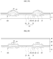
FIG. 6 is a cross-sectional view illustrating an organic light-emitting device according to a second embodiment; and -
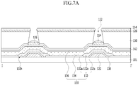
FIGs. 7A to 7D are cross-sectional views for explaining a method of manufacturing the organic light-emitting device illustrated inFIG. 6 . - Hereinafter, exemplary embodiments will be described in detail with reference to the accompanying drawings.
-
FIG. 1 is a plan view illustrating an organic light-emitting device according to an embodiment, andFIG. 2 is a cross-sectional view illustrating the organic light-emitting device ofFIG. 1 . - The organic light-emitting device for a lighting apparatus, illustrated in
FIGs. 1 and2 , includes a light-emittingelement 130, apixel insulation layer 138, and aprotective encapsulation layer 140, which are disposed on asubstrate 101. - The light-emitting
element 130 includes ananode electrode 132, anorganic layer 134 formed on theanode electrode 132, and acathode electrode 136 formed on theorganic layer 134. - The
anode electrode 132 is formed on thesubstrate 101. Theanode electrode 132 is formed of a transparent conductive layer such as indium-tin-oxide (ITO) or indium-zinc-oxide (IZO). Theanode electrode 132, as illustrated inFIG. 3 , includes ananode portion 132a, acontact portion 132b, and a short-circuit-preventingportion 132c. - The
anode portion 132a is an area that overlaps a light-emitting area defined by thepixel insulation layer 138. Theanode portion 132a overlaps thecathode electrode 136 with theorganic layer 134 interposed therebetween. - The
contact portion 132b is formed on a lowerauxiliary electrode 122 so as to extend along the lowerauxiliary electrode 122. Here, the lowerauxiliary electrode 122 is in contact with theanode electrode 132 on the underside of thecontact portion 132b of theanode electrode 132 in order to reduce the resistance of theanode electrode 132. To this end, the lowerauxiliary electrode 122 is formed of a material having conductivity higher than that of the transparent conductive layer of theanode electrode 132. For example, the lowerauxiliary electrode 122 is formed in a single layer or in multiple layers using any one of molybdenum (Mo), aluminum (Al), chrome (Cr), gold (Au), titanium (Ti), nickel (Ni), neodymium (Nd), and copper (Cu), or an alloy thereof. The lowerauxiliary electrode 122 is formed in a lattice form along thepixel insulation layer 138 so as to overlap thepixel insulation layer 138. - The short-circuit-preventing
portion 132c is located between thecontact portion 132b and theanode portion 132a of theanode electrode 132. The short-circuit-preventingportion 132c is spaced apart from each of thecontact portion 132b and theanode portion 132a with ananode hole 132h therebetween in a predetermined area. The short-circuit-preventingportion 132c is formed to have a width smaller than those of thecontact portion 132b and theanode portion 132a so as to have a resistance value higher than those of thecontact portion 132b and theanode portion 132a. Thereby, when a short-circuit defect occurs due to the presence of impurities or the like between thecathode electrode 136 and theanode electrode 132 in a predetermined light-emitting area, the short-circuit-preventingportion 132c prevents current of the light-emittingelement 130 in another light-emitting area from leaking through the short-circuit defect. - Since the
pixel insulation layer 138 is formed along the lowerauxiliary electrode 122 so as to overlap the lowerauxiliary electrode 122, the light-emitting area takes the form of an open island. Thepixel insulation layer 138 is formed so as to cover the side surface and the upper surface of the lowerauxiliary electrode 122 and the side surface of theanode electrode 132. In this case, since the distance between each of theanode electrode 132 and the lowerauxiliary electrode 122 and thecathode electrode 136 is increased by the thickness of thepixel insulation layer 138, compared to the related art, it is possible to reduce the occurrence of short-circuit defects between each of theanode electrode 132 and the lowerauxiliary electrode 122 and thecathode electrode 136. In addition, since thepixel insulation layer 138 is formed so as to cover the side surface of theanode electrode 132, for example, corrosion of theanode electrode 132 may be prevented. Thepixel insulation layer 138 is formed of an organic insulation material having a photoinitiator, for example, photo acryl. Thepixel insulation layer 138, formed of an organic insulation material, may be simply formed through a photolithography process without an etching process, whereby the overall process may be simplified. - The
organic layer 134 is formed on theanode electrode 132 in the light-emitting area defined by thepixel insulation layer 138. Theorganic layer 134 is formed by stacking a hole-related layer, an emission layer, and an electron-related layer in this order or in the reverse order on theanode electrode 132. Since theorganic layer 134 is simply formed through an application process without a photolithography process using an exposure mask or a deposition process using a fine metal mask, theorganic layer 134 is formed below thecathode electrode 136 so as to have an area similar to that of thecathode electrode 136. That is, theorganic layer 134 serves as a waveguide since it is continuously formed over the entire surface of the substrate. Light that is generated in and guided through theorganic layer 134 is extracted to the rear surface of thesubstrate 101 by an upperauxiliary electrode 126, which increases luminous efficacy. - The
cathode electrode 136 is formed on theorganic layer 134 so as to face theanode electrode 132 with theorganic layer 134 interposed therebetween. When applied to a transparent lighting apparatus, thecathode electrode 136 is formed of a transparent conductive layer such as indium-tin-oxide (ITO) or indium-zinc-oxide (IZO), similarly to theanode electrode 132. - In order to reduce the resistance of the
cathode electrode 136, the upperauxiliary electrode 126 is disposed on thecathode electrode 136 so as to come into contact with thecathode electrode 136. The upperauxiliary electrode 126 is formed of a material having conductivity higher than that of the transparent conductive layer of thecathode electrode 136. For example, the upperauxiliary electrode 126 is formed in a single layer or in multiple layers using any one of molybdenum (Mo), aluminum (Al), chrome (Cr), gold (Au), titanium (Ti), nickel (Ni), neodymium (Nd), and copper (Cu), or an alloy thereof. The upperauxiliary electrode 126 is formed in a lattice form or in a straight line form along thepixel insulation layer 138 and the lowerauxiliary electrode 122 so as to overlap thepixel insulation layer 138 and the lowerauxiliary electrode 122. - In the case in which the upper
auxiliary electrode 126 is in contact with theorganic layer 134 below thecathode electrode 136, theorganic layer 134 is damaged by an etching solution, a stripping solution, or the like, which is used in the process of manufacturing the upperauxiliary electrode 126. For this reason, since the upperauxiliary electrode 126 is disposed on thecathode electrode 136 and is not in contact with theorganic layer 134, it is possible to prevent damage to theorganic layer 134 in the process of manufacturing the upperauxiliary electrode 126. - In addition, since the upper
auxiliary electrode 126 is formed of an opaque material, the upperauxiliary electrode 126 serves as a reflector. In this case, the upperauxiliary electrode 126 reflects the light that is generated in theorganic layer 134 and directed to the upperauxiliary electrode 126, so as to cause the light to be emitted outwards through thesubstrate 101, which may increase light extraction efficiency. - A
protective metal layer 114 is disposed on the upperauxiliary electrode 126 to have the same width as that of the upperauxiliary electrode 126. Theprotective metal layer 114 is provided to form a boundary with theprotective encapsulation layer 140. Theprotective metal layer 114 is formed of a material having lower adsorption on an organic polymer layer (e.g. a photoresist), compared to an inorganic insulation material or a metal material. For example, theprotective metal layer 114 is formed of Al2O3. Theprotective metal layer 114 serves to prevent damage to the upperauxiliary electrode 126 and theorganic layer 134 by a solution used in a manufacturing process thereof. - The
protective encapsulation layer 140 prevents external moisture or oxygen from being introduced into the organic light-emittingelement 130, which is vulnerable to external moisture or oxygen. To this end, theprotective encapsulation layer 140 is disposed on thecathode electrode 136 to encapsulate theorganic layer 134, which is vulnerable to moisture or oxygen. Theprotective encapsulation layer 140 includes atrench 148, which exposes the upper surface of thecathode electrode 136, in the area in which theprotective encapsulation layer 140 overlaps the lowerauxiliary electrode 122. The upperauxiliary electrode 126 is buried in thetrench 148 to form a boundary with theprotective encapsulation layer 140. - The
protective encapsulation layer 140 may be formed in a single layer, as illustrated inFIG. 2 , or may be formed in multiple layers, as illustrated inFIG. 4 . - The
protective encapsulation layer 140 illustrated inFIG. 4 includes a plurality of inorganic encapsulation layers 142 and 146 and anorganic encapsulation layer 144 disposed between the inorganic encapsulation layers 142 and 146, and theinorganic encapsulation layer 146 is disposed in the uppermost layer. Here, theprotective encapsulation layer 140 includes at least two inorganic encapsulation layers 142 and 146 and at least oneorganic encapsulation layer 144. The structure of theprotective encapsulation layer 140 in which theorganic encapsulation layer 144 is disposed between first and second inorganic encapsulation layers 142 and 146 will be described by way of example. - The first
inorganic encapsulation layer 142 is formed on thesubstrate 101, on which thecathode electrode 136 is formed, so as to be closest to the organic light-emittingelement 130. The firstinorganic encapsulation layer 142 is formed of an inorganic insulation material that enables low-temperature deposition, such as silicon nitride (SiNx), silicon oxide (SiOx), silicon oxide nitride (SiON), or aluminum oxide (Al2O3). Thereby, since the firstinorganic encapsulation layer 142 is deposited under a low-temperature atmosphere, it is possible to prevent damage to theorganic layer 134, which is vulnerable to a high-temperature atmosphere during deposition of the firstinorganic encapsulation layer 142. - The first
inorganic encapsulation layer 142 includes thetrench 148, which exposes the upper surface of thecathode electrode 136, in the area in which the firstinorganic encapsulation layer 142 overlaps the lowerauxiliary electrode 122. The upperauxiliary electrode 126 is buried in thetrench 148 to form a boundary with the firstinorganic encapsulation layer 142. - The
organic encapsulation layer 144 is disposed on the firstinorganic encapsulation layer 142 so as to have an area smaller than that of the firstinorganic encapsulation layer 142. Theorganic encapsulation layer 144 is formed of an organic insulation material such as acryl resin, epoxy resin, polyimide, polyethylene, or silicon oxycarbon (SiOC). Thereby, theorganic encapsulation layer 144 serves to alleviate stress between the respective layers caused by bending of the organic light-emitting device, and increases planarization performance. - The second
inorganic encapsulation layer 146 is formed on thesubstrate 101 having theorganic encapsulation layer 144 formed thereon, so as to cover the upper surface and the side surface of theorganic encapsulation layer 144. Thereby, the secondinorganic encapsulation layer 146 minimizes or prevents external moisture or oxygen from being introduced into the firstinorganic encapsulation layer 142 and theorganic encapsulation layer 144. The secondinorganic encapsulation layer 146 is formed of an inorganic insulation material, such as silicon nitride (SiNx), silicon oxide (SiOx), silicon oxide nitride (SiON), or aluminum oxide (Al2O3). -
FIGs. 5A to 5H are cross-sectional views for explaining a method of manufacturing the organic light-emitting device illustrated inFIG. 4 . - As illustrated in
FIG. 5A , after an opaque conductive layer is deposited over the entire surface of thesubstrate 101, the opaque conductive layer is patterned through a photolithography process and an etching process, so that the lower auxiliary electrode is formed. Subsequently, after a transparent conductive layer is deposited over the entire surface of thesubstrate 101 having the lower auxiliary electrode formed thereon, the transparent conductive layer is patterned through a photolithography process and an etching process, so that theanode electrode 132, which includes theanode portion 132a, the short-circuit-preventingportion 132c, and thecontact portion 132b, is formed. After an inorganic insulation material, such as SiNx or SiOx, is deposited over the entire surface of thesubstrate 101 having theanode electrode 132 formed thereon, the inorganic insulation material is patterned through a photolithography process and an etching process, so that thepixel insulation layer 138 is formed, as illustrated inFIG. 5B . As illustrated inFIG. 5C , theorganic layer 134, thecathode electrode 136, and the firstinorganic encapsulation layer 142 are sequentially formed over the entire surface of thesubstrate 101 having thepixel insulation layer 138 formed thereon. Subsequently, after a photoresist is applied on the firstinorganic encapsulation layer 142, the photoresist is patterned through an exposure process and a developing process, so that aphotoresist pattern 150 having anopening 152 is formed. Here, theopening 152 is located so as to overlap thepixel insulation layer 138, and the side surface of thephotoresist pattern 150, exposed through theopening 152, is formed to have an inversely tapered shape. - When the first
inorganic encapsulation layer 142 is patterned through an etching process using thephotoresist pattern 150 as a mask, as illustrated inFIG. 5D , thetrench 148 is formed to expose thecathode electrode 136. - Subsequently, when an opaque conductive layer is deposited over the entire surface of the
substrate 101 having thetrench 148 formed therein, as illustrated inFIG. 5E , the upperauxiliary electrode 126 is formed on thephotoresist pattern 150 and the upperauxiliary electrode 126 is buried in thetrench 148. At this time, the upperauxiliary electrode 126 is formed so as to expose the side surface of thephotoresist pattern 150. - Subsequently, as illustrated in
FIG. 5F , theprotective metal layer 114 is deposited over the entire surface of thesubstrate 101 having the upperauxiliary electrode 126 formed thereon. At this time, theprotective metal layer 114 is formed of a material having higher adhesion to the upperauxiliary electrode 126 than to thephotoresist pattern 150 formed of an organic insulation material. Thereby, theprotective metal layer 114 is formed on the upper surface of the upperauxiliary electrode 126, but is not formed on the side surface of thephotoresist pattern 150. Subsequently, as illustrated inFIG. 5G , thephotoresist pattern 150 is removed through a stripping process, so that the upperauxiliary electrode 126 and theprotective metal layer 114 disposed on thephotoresist pattern 150 are removed. In the stripping process, the side surface of thephotoresist pattern 150 is exposed outwards, which enables easy removal of thephotoresist pattern 150. - Subsequently, as illustrated in
FIG. 5H , theorganic encapsulation layer 144 and the secondinorganic encapsulation layer 146 are sequentially stacked on thesubstrate 101 having theprotective metal layer 114. - In this way, the organic light-emitting device according to embodiments may simplify the manufacturing process thereof and consequently reduce costs, since the
protective metal layer 114 and the upperauxiliary electrode 126 are formed through the same mask process. -
FIG. 6 is a cross-sectional view illustrating an organic light-emitting device according to a second embodiment. - The organic light-emitting device illustrated in
FIG. 6 includes the same constituent elements as those of the organic light-emitting device illustrated inFIG. 2 , except that it further includes a secondprotective metal layer 124. Thus, a detailed description related to the same constituent elements will be omitted below. - The second
protective metal layer 124 is disposed on theprotective metal layer 114 to have a width larger than that of theprotective metal layer 114. Since the secondprotective metal layer 124 has an area larger than that of theprotective metal layer 114, the secondprotective metal layer 124 is formed so as to cover the side surface of theprotective metal layer 114. Thereby, the secondprotective metal layer 124 is formed so as to cover a gap between the upperauxiliary electrode 126 and theprotective metal layer 114, thereby preventing a manufacturing solution (e.g. a washing solution, an etching solution, or a stripping solution) from being introduced into the gap between the upperauxiliary electrode 126 and theprotective metal layer 114 during the manufacturing process thereof. - The second
protective metal layer 124 is formed of the same material as, or a different material from theprotective metal layer 114. For example, the secondprotective metal layer 124 is formed of Al2O3, similarly to theprotective metal layer 114. -
FIGs. 7A to 7D are cross-sectional views for explaining a method of manufacturing the organic light-emitting device illustrated inFIG. 6 . It is to be noted that the method of manufacturing the organic light-emitting device illustrated inFIG. 6 up to the formation of theprotective metal layer 114 is the same as the method for the organic light-emitting device illustrated inFIG. 2 , and thus a detailed description thereof will be omitted below. - That is, as illustrated in
FIG. 7A , the upperauxiliary electrode 126 and theprotective metal layer 114 are formed on thesubstrate 101 via the manufacturing method illustrated inFIGs. 5A to 5H . - Subsequently, as illustrated in
FIG. 7B , thephotoresist pattern 150 is etched through an etching process. At this time, excluding the upper surface of thephotoresist pattern 150, which is protected by theprotective metal layer 114 and the upperauxiliary electrode 126, the side surface of thephotoresist pattern 150 is etched. Thus, theopening 152 in thephotoresist pattern 150 is wider than that of theprotective metal layer 114. - Subsequently, as illustrated in
FIG. 7C , the secondprotective metal layer 124 is deposited over the entire surface of theprotective metal layer 114. At this time, the secondprotective metal layer 124 is formed of a material having higher adhesion to theprotective metal layer 114 and the upperauxiliary electrode 126 than to thephotoresist pattern 150 formed of an organic insulation material. Thereby, the secondprotective metal layer 124 is formed on the upper surface of theprotective metal layer 114, but is not formed on the side surface of thephotoresist pattern 150. Subsequently, as illustrated inFIG. 7D , by removing thephotoresist pattern 150 through a stripping process, the upperauxiliary electrode 126, theprotective metal layer 114, and the secondprotective metal layer 124, which are disposed on thephotoresist pattern 150, are removed. - Subsequently, the
organic encapsulation layer 144 and the secondinorganic encapsulation layer 146 are sequentially stacked on thesubstrate 101 having theprotective metal layer 114 and the secondprotective metal layer 124 formed thereon. - In this way, the organic light-emitting device according to embodiments may simplify the manufacturing process thereof and consequently, reduce costs since the
protective metal layer 114, the secondprotective metal layer 124, and the upperauxiliary electrode 126 are formed through the same mask process. - As is apparent from the above description, according to the embodiments, a lower auxiliary electrode is directly disposed on an anode electrode and an upper auxiliary electrode is directly disposed on a cathode electrode, whereby it is possible to reduce the resistance of each of the anode electrode and the cathode electrode without damage to an organic layer, which may prevent brightness uniformity. In addition, by disposing a protective metal layer on the upper auxiliary electrode, which is buried in a trench in a protective encapsulation layer, it is possible to prevent damage to the organic layer by external moisture, oxygen, or the like. In addition, the upper auxiliary electrode and the protective metal layer are formed through the same mask process, which may result in a simplified structure and reduced manufacturing costs. Moreover, the upper auxiliary electrode serves as a reflective electrode to improve light extraction, which results in increased luminous efficacy.
- Although the embodiments have been described above in detail with reference to the accompanying drawings, it will be apparent to those skilled in the art that the scope of the appended claims is not limited to the embodiments described above, and various substitutions, modifications, and alterations may be made to the described embodiments without departing from the scope of the appended claims.
- Also described herein are the following numbered clauses:
- Clause 1. An organic light-emitting device comprising:
- an anode electrode;
- an organic layer disposed on the anode electrode;
- a cathode electrode disposed to face the anode electrode with the organic layer interposed therebetween;
- a protective encapsulation layer disposed on the cathode electrode and comprising a trench; and
- an upper auxiliary electrode buried in the trench to come into contact with the cathode electrode.
- Clause 2. The device according to clause 1, further comprising a protective metal layer disposed on an upper surface of the upper auxiliary electrode and having the same width as that of the upper auxiliary electrode.
- Clause 3. The device according to clause 2, wherein the protective metal layer is formed of a material having lower adsorption on an organic polymer layer, compared to an inorganic insulation material or a metal material.
-
Clause 4. The device according to clause 2 or 3, wherein the protective metal layer is formed of Al2O3. - Clause 5. The device according to
clause 2, 3 or 4, further comprising a second protective metal layer disposed on the protective metal layer and having a width larger than that of the protective metal layer to cover a side surface of the protective metal layer. - Clause 6. The device according to clause 5, wherein the protective metal layer and the second protective metal layer have higher adhesion to the upper auxiliary electrode than adhesion to an organic insulation material.
- Clause 7. The device according to clause 5 or 6, wherein the second protective metal layer is formed of Al2O3.
- Clause 8. The device according to any preceding clause, further comprising a lower auxiliary electrode disposed below the anode electrode to come into contact with the anode electrode.
- Clause 9. The device according to clause 8, wherein the lower auxiliary electrode overlaps the trench.
- Clause 10. The device according to any preceding clause, wherein the protective encapsulation layer comprises:
- a first inorganic encapsulation layer disposed on the cathode electrode;
- an organic encapsulation layer disposed on the first inorganic encapsulation layer; and
- a second inorganic encapsulation layer disposed on the organic encapsulation layer, and
- wherein the first inorganic encapsulation layer comprises the trench.
Claims (14)
- An organic light-emitting device comprising:a substrate (101);an anode electrode (132) on the substrate;an organic layer (134) disposed on the anode electrode;a cathode electrode (136) disposed to face the anode electrode with the organic layer interposed therebetween;a protective encapsulation layer (142) disposed on the cathode electrode and comprising a trench (148); andan upper auxiliary electrode (126) disposed in the trench to come into contact with the cathode electrode.
- The device according to claim 1, further comprising a first protective metal layer (114) disposed on an upper surface of the upper auxiliary electrode (126) and having the same width as that of the upper auxiliary electrode.
- The device according to claim 2, wherein the first protective metal layer (114) is formed of a material having lower adsorption on an organic polymer layer, compared with an inorganic insulation material or a metal material.
- The device according to claim 2 or 3, wherein the first protective metal layer (114) is formed of Al2O3.
- The device according to claim 2, 3 or 4, wherein the first protective metal layer (114) has higher adhesion to the upper auxiliary electrode (126) than adhesion to an organic insulation material.
- The device according to any of claims 2-5, further comprising a second protective metal layer (124) disposed on the first protective metal layer (114) and having a width larger than that of the first protective metal layer to cover a side surface of the first protective metal layer.
- The device according to claim 6, wherein the second protective metal layer (124) has higher adhesion to the upper auxiliary electrode (126) than adhesion to an organic insulation material.
- The device according to claim 6 or 7, wherein the second protective metal layer (124) has higher adhesion to the first protective layer (114) than adhesion to an organic insulation material.
- The device according to claim 6, 7 or 8, wherein the second protective metal layer (124) is formed of Al2O3.
- The device according to any preceding claim, further comprising a lower auxiliary electrode (122) disposed below the anode electrode (132) to come into contact with the anode electrode.
- The device according to claim 10, wherein the lower auxiliary electrode (122) overlaps the trench (148).
- The device according to claim 10 or 11, further comprising a pixel insulation layer (138) disposed on the lower auxiliary electrode (122) and defining a light-emitting area; and
wherein the anode electrode (132) comprises:an anode portion (132a) overlapping the light-emitting area;a contact portion (132b) formed between the lower auxiliary electrode (122) and the pixel insulation layer (138); anda short circuit preventing portion (132c) disposed between and spaced apart from the anode portion and the contact portion. - The device according to any preceding claim, wherein the protective encapsulation layer (142) is a first inorganic encapsulation layer (142);
wherein the device further comprises:an organic encapsulation layer (144) disposed on the protective encapsulation layer (142); anda second inorganic encapsulation layer (146) disposed on the organic encapsulation layer (144). - A method of manufacturing an organic light-emitting device, the method comprising:providing a substrate (101);forming an anode electrode (132) on the substrate;forming an organic layer (134) on the anode electrode (132);forming a cathode electrode (136) to face the anode electrode with the organic layer interposed therebetween;forming a protective encapsulation layer (142) on the cathode electrode;forming a trench (148) in the protective encapsulation layer (140) so as to expose an upper surface of the cathode electrode; andforming an upper auxiliary electrode (126) in the trench and in contact with the cathode electrode.
Applications Claiming Priority (1)
| Application Number | Priority Date | Filing Date | Title |
|---|---|---|---|
| KR1020170160417A KR102450339B1 (en) | 2017-11-28 | 2017-11-28 | Organic light emitting device |
Publications (1)
| Publication Number | Publication Date |
|---|---|
| EP3490022A1 true EP3490022A1 (en) | 2019-05-29 |
Family
ID=64500200
Family Applications (1)
| Application Number | Title | Priority Date | Filing Date |
|---|---|---|---|
| EP18208472.3A Pending EP3490022A1 (en) | 2017-11-28 | 2018-11-27 | Organic light-emitting device |
Country Status (6)
| Country | Link |
|---|---|
| US (1) | US10636995B2 (en) |
| EP (1) | EP3490022A1 (en) |
| JP (1) | JP6681455B2 (en) |
| KR (1) | KR102450339B1 (en) |
| CN (1) | CN109841749B (en) |
| TW (1) | TWI671930B (en) |
Cited By (1)
| Publication number | Priority date | Publication date | Assignee | Title |
|---|---|---|---|---|
| US12598889B2 (en) | 2021-06-30 | 2026-04-07 | Boe Technology Group Co., Ltd. | Display panel and manufacturing method therefor, and display device |
Families Citing this family (8)
| Publication number | Priority date | Publication date | Assignee | Title |
|---|---|---|---|---|
| CN108511629A (en) * | 2018-05-31 | 2018-09-07 | 京东方科技集团股份有限公司 | Oled display substrate and preparation method thereof, display device |
| KR102711344B1 (en) * | 2019-06-11 | 2024-09-27 | 엘지디스플레이 주식회사 | Electronic device |
| US12532612B2 (en) | 2020-02-26 | 2026-01-20 | Sharp Kabushiki Kaisha | Display device with overlapping contact holes exposing edge of an insulator and method for manufacturing same |
| CN111477664B (en) * | 2020-04-26 | 2023-11-24 | 合肥鑫晟光电科技有限公司 | A display panel and its manufacturing method and display device |
| CN111682121A (en) * | 2020-06-23 | 2020-09-18 | 京东方科技集团股份有限公司 | Display backplane, method of making the same, and display device |
| CN112366279A (en) * | 2020-10-27 | 2021-02-12 | 合肥京东方卓印科技有限公司 | Display panel, display device and manufacturing method of display panel |
| CN116828935A (en) * | 2022-01-04 | 2023-09-29 | 台州观宇科技有限公司 | Display device and method of manufacturing display device |
| CN114843420A (en) * | 2022-04-20 | 2022-08-02 | 深圳市华星光电半导体显示技术有限公司 | Display panel, manufacturing method of display panel and display device |
Citations (4)
| Publication number | Priority date | Publication date | Assignee | Title |
|---|---|---|---|---|
| US20020011783A1 (en) * | 2000-02-16 | 2002-01-31 | Idemitsu Kosan Co., Ltd | Active-driving organic el light emission device and process for producing the same |
| EP2985803A1 (en) * | 2013-05-16 | 2016-02-17 | LG Chem, Ltd. | Organic light-emitting device and method of manufacturing same |
| US20170084859A1 (en) * | 2014-03-19 | 2017-03-23 | Osram Oled Gmbh | Optoelectronic component and method for producing an optoelectronic component |
| EP3331039A1 (en) * | 2016-11-30 | 2018-06-06 | LG Display Co., Ltd. | Lighting apparatus using organic light-emitting diode and method of fabricating the same |
Family Cites Families (14)
| Publication number | Priority date | Publication date | Assignee | Title |
|---|---|---|---|---|
| JP4519532B2 (en) * | 2003-06-16 | 2010-08-04 | 株式会社半導体エネルギー研究所 | LIGHT EMITTING DEVICE AND ELECTRONIC DEVICE USING LIGHT EMITTING DEVICE |
| JP2006261058A (en) * | 2005-03-18 | 2006-09-28 | Sony Corp | ORGANIC EL ELEMENT, DISPLAY DEVICE, ORGANIC EL ELEMENT MANUFACTURING METHOD |
| CN101330131B (en) * | 2007-06-20 | 2010-08-18 | 中国南玻集团股份有限公司 | Organic electroluminescent display device, transparent conductive film substrate and preparation method |
| JP2009048860A (en) * | 2007-08-20 | 2009-03-05 | Hitachi Displays Ltd | Organic electroluminescence display device |
| US8552440B2 (en) * | 2010-12-24 | 2013-10-08 | Semiconductor Energy Laboratory Co., Ltd. | Lighting device |
| WO2012086758A1 (en) * | 2010-12-24 | 2012-06-28 | Necライティング株式会社 | Organic electroluminescent element and organic electroluminescent lighting device |
| KR101983230B1 (en) * | 2012-10-19 | 2019-05-29 | 삼성디스플레이 주식회사 | Organic light emitting display device and the manufacturing method thereof |
| KR101407590B1 (en) * | 2012-11-19 | 2014-06-13 | 삼성디스플레이 주식회사 | Organic light emitting display device and the manufacturing method thereof |
| KR102117607B1 (en) * | 2013-07-23 | 2020-06-02 | 삼성디스플레이 주식회사 | Organic light emitting display device and manufacturing method thereof |
| JP6487173B2 (en) * | 2014-10-08 | 2019-03-20 | 株式会社ジャパンディスプレイ | Display device and manufacturing method thereof |
| KR20160047673A (en) * | 2014-10-22 | 2016-05-03 | 삼성디스플레이 주식회사 | Organic light emitting display apparatus and the fabrication method thereof |
| JP2016207452A (en) * | 2015-04-22 | 2016-12-08 | ソニー株式会社 | Manufacturing method of display device, display device, and electronic equipment |
| WO2017056814A1 (en) * | 2015-09-30 | 2017-04-06 | コニカミノルタ株式会社 | Transparent organic electroluminescence element and method for manufacturing same |
| KR102460407B1 (en) * | 2015-10-30 | 2022-10-27 | 엘지디스플레이 주식회사 | Organic light emitting display device and method of manufacturing the same |
-
2017
- 2017-11-28 KR KR1020170160417A patent/KR102450339B1/en active Active
-
2018
- 2018-11-06 TW TW107139360A patent/TWI671930B/en active
- 2018-11-13 CN CN201811346145.1A patent/CN109841749B/en active Active
- 2018-11-21 JP JP2018218186A patent/JP6681455B2/en active Active
- 2018-11-26 US US16/199,683 patent/US10636995B2/en active Active
- 2018-11-27 EP EP18208472.3A patent/EP3490022A1/en active Pending
Patent Citations (4)
| Publication number | Priority date | Publication date | Assignee | Title |
|---|---|---|---|---|
| US20020011783A1 (en) * | 2000-02-16 | 2002-01-31 | Idemitsu Kosan Co., Ltd | Active-driving organic el light emission device and process for producing the same |
| EP2985803A1 (en) * | 2013-05-16 | 2016-02-17 | LG Chem, Ltd. | Organic light-emitting device and method of manufacturing same |
| US20170084859A1 (en) * | 2014-03-19 | 2017-03-23 | Osram Oled Gmbh | Optoelectronic component and method for producing an optoelectronic component |
| EP3331039A1 (en) * | 2016-11-30 | 2018-06-06 | LG Display Co., Ltd. | Lighting apparatus using organic light-emitting diode and method of fabricating the same |
Cited By (1)
| Publication number | Priority date | Publication date | Assignee | Title |
|---|---|---|---|---|
| US12598889B2 (en) | 2021-06-30 | 2026-04-07 | Boe Technology Group Co., Ltd. | Display panel and manufacturing method therefor, and display device |
Also Published As
| Publication number | Publication date |
|---|---|
| JP2019102446A (en) | 2019-06-24 |
| TWI671930B (en) | 2019-09-11 |
| KR20190061739A (en) | 2019-06-05 |
| KR102450339B1 (en) | 2022-10-04 |
| TW201926757A (en) | 2019-07-01 |
| US20190165298A1 (en) | 2019-05-30 |
| US10636995B2 (en) | 2020-04-28 |
| CN109841749A (en) | 2019-06-04 |
| CN109841749B (en) | 2021-01-29 |
| JP6681455B2 (en) | 2020-04-15 |
Similar Documents
| Publication | Publication Date | Title |
|---|---|---|
| US10636995B2 (en) | Organic light-emitting device | |
| US11114519B2 (en) | Organic light emitting display device and method of manufacturing the same | |
| US11189814B2 (en) | Organic light emitting display apparatus and method of manufacturing the same | |
| KR102458907B1 (en) | Organic light emitting display and method of fabricating the same | |
| US10797124B2 (en) | Organic light emitting display substrate and manufacturing method thereof | |
| CN108074953B (en) | Organic light-emitting display device and manufacturing method thereof | |
| KR101980780B1 (en) | Organic light emitting display device and method of manufacturing the same | |
| EP3163624B1 (en) | Organic light emitting display device and method of manufacturing the same | |
| US9825262B2 (en) | Organic light emitting display apparatus and method of manufacturing the same | |
| KR102453921B1 (en) | Organic light emitting display and manufacturing method thereof | |
| KR102421576B1 (en) | Organic light-emitting apparatus and the method for manufacturing of the organic light-emitting display apparatus | |
| KR20100062566A (en) | Top emission type organic electro luminescent device and methode of fabricating the same | |
| KR20210099542A (en) | Organic light emitting display apparatus and the fabrication method thereof | |
| KR102482986B1 (en) | Organic light emitting display device and method of manufacturing the same | |
| KR20180036465A (en) | Organic light emitting display device and method of manufacturing the same | |
| KR102220787B1 (en) | Organic Light Emitting Display Device and Method for Manufacturing The Same | |
| KR102340734B1 (en) | Organic light emitting display device and method of manufacturing the same | |
| KR102347847B1 (en) | Organic light emitting display device | |
| KR102295260B1 (en) | Organic light emitting display device and method of manufacturing the same | |
| KR102577245B1 (en) | Organic light emitting display device and method of manufacturing the same | |
| KR20240076155A (en) | Organic light emitting display apparatus | |
| KR20230099873A (en) | Display device and manufacturing method of the same |
Legal Events
| Date | Code | Title | Description |
|---|---|---|---|
| PUAI | Public reference made under article 153(3) epc to a published international application that has entered the european phase |
Free format text: ORIGINAL CODE: 0009012 |
|
| STAA | Information on the status of an ep patent application or granted ep patent |
Free format text: STATUS: REQUEST FOR EXAMINATION WAS MADE |
|
| 17P | Request for examination filed |
Effective date: 20181127 |
|
| AK | Designated contracting states |
Kind code of ref document: A1 Designated state(s): AL AT BE BG CH CY CZ DE DK EE ES FI FR GB GR HR HU IE IS IT LI LT LU LV MC MK MT NL NO PL PT RO RS SE SI SK SM TR |
|
| AX | Request for extension of the european patent |
Extension state: BA ME |
|
| RBV | Designated contracting states (corrected) |
Designated state(s): AL AT BE BG CH CY CZ DE DK EE ES FI FR GB GR HR HU IE IS IT LI LT LU LV MC MK MT NL NO PL PT RO RS SE SI SK SM TR |