EP3483656B1 - Pellicle for euv lithography - Google Patents
Pellicle for euv lithography Download PDFInfo
- Publication number
- EP3483656B1 EP3483656B1 EP18165360.1A EP18165360A EP3483656B1 EP 3483656 B1 EP3483656 B1 EP 3483656B1 EP 18165360 A EP18165360 A EP 18165360A EP 3483656 B1 EP3483656 B1 EP 3483656B1
- Authority
- EP
- European Patent Office
- Prior art keywords
- layer
- pellicle
- etching
- silicon
- pattern
- Prior art date
- Legal status (The legal status is an assumption and is not a legal conclusion. Google has not performed a legal analysis and makes no representation as to the accuracy of the status listed.)
- Active
Links
Images





Classifications
-
- G—PHYSICS
- G03—PHOTOGRAPHY; CINEMATOGRAPHY; ANALOGOUS TECHNIQUES USING WAVES OTHER THAN OPTICAL WAVES; ELECTROGRAPHY; HOLOGRAPHY
- G03F—PHOTOMECHANICAL PRODUCTION OF TEXTURED OR PATTERNED SURFACES, e.g. FOR PRINTING, FOR PROCESSING OF SEMICONDUCTOR DEVICES; MATERIALS THEREFOR; ORIGINALS THEREFOR; APPARATUS SPECIALLY ADAPTED THEREFOR
- G03F1/00—Originals for photomechanical production of textured or patterned surfaces, e.g., masks, photo-masks, reticles; Mask blanks or pellicles therefor; Containers specially adapted therefor; Preparation thereof
- G03F1/66—Containers specially adapted for masks, mask blanks or pellicles; Preparation thereof
-
- G—PHYSICS
- G03—PHOTOGRAPHY; CINEMATOGRAPHY; ANALOGOUS TECHNIQUES USING WAVES OTHER THAN OPTICAL WAVES; ELECTROGRAPHY; HOLOGRAPHY
- G03F—PHOTOMECHANICAL PRODUCTION OF TEXTURED OR PATTERNED SURFACES, e.g. FOR PRINTING, FOR PROCESSING OF SEMICONDUCTOR DEVICES; MATERIALS THEREFOR; ORIGINALS THEREFOR; APPARATUS SPECIALLY ADAPTED THEREFOR
- G03F1/00—Originals for photomechanical production of textured or patterned surfaces, e.g., masks, photo-masks, reticles; Mask blanks or pellicles therefor; Containers specially adapted therefor; Preparation thereof
- G03F1/22—Masks or mask blanks for imaging by radiation of 100nm or shorter wavelength, e.g. X-ray masks, extreme ultraviolet [EUV] masks; Preparation thereof
-
- G—PHYSICS
- G03—PHOTOGRAPHY; CINEMATOGRAPHY; ANALOGOUS TECHNIQUES USING WAVES OTHER THAN OPTICAL WAVES; ELECTROGRAPHY; HOLOGRAPHY
- G03F—PHOTOMECHANICAL PRODUCTION OF TEXTURED OR PATTERNED SURFACES, e.g. FOR PRINTING, FOR PROCESSING OF SEMICONDUCTOR DEVICES; MATERIALS THEREFOR; ORIGINALS THEREFOR; APPARATUS SPECIALLY ADAPTED THEREFOR
- G03F1/00—Originals for photomechanical production of textured or patterned surfaces, e.g., masks, photo-masks, reticles; Mask blanks or pellicles therefor; Containers specially adapted therefor; Preparation thereof
- G03F1/62—Pellicles, e.g. pellicle assemblies, e.g. having membrane on support frame; Preparation thereof
-
- G—PHYSICS
- G03—PHOTOGRAPHY; CINEMATOGRAPHY; ANALOGOUS TECHNIQUES USING WAVES OTHER THAN OPTICAL WAVES; ELECTROGRAPHY; HOLOGRAPHY
- G03F—PHOTOMECHANICAL PRODUCTION OF TEXTURED OR PATTERNED SURFACES, e.g. FOR PRINTING, FOR PROCESSING OF SEMICONDUCTOR DEVICES; MATERIALS THEREFOR; ORIGINALS THEREFOR; APPARATUS SPECIALLY ADAPTED THEREFOR
- G03F1/00—Originals for photomechanical production of textured or patterned surfaces, e.g., masks, photo-masks, reticles; Mask blanks or pellicles therefor; Containers specially adapted therefor; Preparation thereof
- G03F1/38—Masks having auxiliary features, e.g. special coatings or marks for alignment or testing; Preparation thereof
-
- G—PHYSICS
- G03—PHOTOGRAPHY; CINEMATOGRAPHY; ANALOGOUS TECHNIQUES USING WAVES OTHER THAN OPTICAL WAVES; ELECTROGRAPHY; HOLOGRAPHY
- G03F—PHOTOMECHANICAL PRODUCTION OF TEXTURED OR PATTERNED SURFACES, e.g. FOR PRINTING, FOR PROCESSING OF SEMICONDUCTOR DEVICES; MATERIALS THEREFOR; ORIGINALS THEREFOR; APPARATUS SPECIALLY ADAPTED THEREFOR
- G03F1/00—Originals for photomechanical production of textured or patterned surfaces, e.g., masks, photo-masks, reticles; Mask blanks or pellicles therefor; Containers specially adapted therefor; Preparation thereof
- G03F1/62—Pellicles, e.g. pellicle assemblies, e.g. having membrane on support frame; Preparation thereof
- G03F1/64—Pellicles, e.g. pellicle assemblies, e.g. having membrane on support frame; Preparation thereof characterised by the frames, e.g. structure or material, including bonding means therefor
-
- G—PHYSICS
- G03—PHOTOGRAPHY; CINEMATOGRAPHY; ANALOGOUS TECHNIQUES USING WAVES OTHER THAN OPTICAL WAVES; ELECTROGRAPHY; HOLOGRAPHY
- G03F—PHOTOMECHANICAL PRODUCTION OF TEXTURED OR PATTERNED SURFACES, e.g. FOR PRINTING, FOR PROCESSING OF SEMICONDUCTOR DEVICES; MATERIALS THEREFOR; ORIGINALS THEREFOR; APPARATUS SPECIALLY ADAPTED THEREFOR
- G03F7/00—Photomechanical, e.g. photolithographic, production of textured or patterned surfaces, e.g. printing surfaces; Materials therefor, e.g. comprising photoresists; Apparatus specially adapted therefor
- G03F7/70—Microphotolithographic exposure; Apparatus therefor
- G03F7/70008—Production of exposure light, i.e. light sources
- G03F7/70033—Production of exposure light, i.e. light sources by plasma extreme ultraviolet [EUV] sources
-
- G—PHYSICS
- G03—PHOTOGRAPHY; CINEMATOGRAPHY; ANALOGOUS TECHNIQUES USING WAVES OTHER THAN OPTICAL WAVES; ELECTROGRAPHY; HOLOGRAPHY
- G03F—PHOTOMECHANICAL PRODUCTION OF TEXTURED OR PATTERNED SURFACES, e.g. FOR PRINTING, FOR PROCESSING OF SEMICONDUCTOR DEVICES; MATERIALS THEREFOR; ORIGINALS THEREFOR; APPARATUS SPECIALLY ADAPTED THEREFOR
- G03F7/00—Photomechanical, e.g. photolithographic, production of textured or patterned surfaces, e.g. printing surfaces; Materials therefor, e.g. comprising photoresists; Apparatus specially adapted therefor
- G03F7/70—Microphotolithographic exposure; Apparatus therefor
- G03F7/708—Construction of apparatus, e.g. environment aspects, hygiene aspects or materials
- G03F7/70983—Optical system protection, e.g. pellicles or removable covers for protection of mask
-
- H—ELECTRICITY
- H10—SEMICONDUCTOR DEVICES; ELECTRIC SOLID-STATE DEVICES NOT OTHERWISE PROVIDED FOR
- H10P—GENERIC PROCESSES OR APPARATUS FOR THE MANUFACTURE OR TREATMENT OF DEVICES COVERED BY CLASS H10
- H10P76/00—Manufacture or treatment of masks on semiconductor bodies, e.g. by lithography or photolithography
- H10P76/20—Manufacture or treatment of masks on semiconductor bodies, e.g. by lithography or photolithography of masks comprising organic materials
- H10P76/204—Manufacture or treatment of masks on semiconductor bodies, e.g. by lithography or photolithography of masks comprising organic materials of organic photoresist masks
- H10P76/2041—Photolithographic processes
-
- H—ELECTRICITY
- H10—SEMICONDUCTOR DEVICES; ELECTRIC SOLID-STATE DEVICES NOT OTHERWISE PROVIDED FOR
- H10W—GENERIC PACKAGES, INTERCONNECTIONS, CONNECTORS OR OTHER CONSTRUCTIONAL DETAILS OF DEVICES COVERED BY CLASS H10
- H10W20/00—Interconnections in chips, wafers or substrates
- H10W20/01—Manufacture or treatment
- H10W20/071—Manufacture or treatment of dielectric parts thereof
- H10W20/074—Manufacture or treatment of dielectric parts thereof of dielectric parts comprising thin functional dielectric layers, e.g. dielectric etch-stop, barrier, capping or liner layers
Definitions
- the present disclosure relates to a pellicle for extreme ultraviolet (EUV) lithography and a method of fabricating the same, and more particularly to a pellicle for EUV lithography, which has high transmittance to EUV exposure light and is improved in mechanical strength, and a method of fabricating the same.
- EUV extreme ultraviolet
- a currently commercialized exposure process employs exposure equipment using an ArF wavelength range of 193nm to perform a transfer process and form a fine pattern on a wafer, but is limited in terms of forming a fine pattern of 32nm or less. Accordingly, there have been developed various methods such as immersion lithography of using a liquid medium having a higher refractive index (e.g. 1.44) than air; double lithography of performing exposure twice; phase shift technology of shifting a phase of light by 180 degrees and causing a destructive interference with adjacent transmission light; optical phase correction of correcting a small size or rounded end of a designed pattern caused by the interference and diffraction of light; etc.
- immersion lithography of using a liquid medium having a higher refractive index (e.g. 1.44) than air
- double lithography of performing exposure twice phase shift technology of shifting a phase of light by 180 degrees and causing a destructive interference with adjacent transmission light
- optical phase correction of correcting a small size or rounded end of a designed pattern caused by the interference
- EUV extreme ultraviolet
- the lithography process employs a photomask as an original plate for patterning, and a pattern on the photomask is transferred to a wafer.
- the photomask is attached with impurities such as particles, foreign materials, etc., the impurities may damage the pattern transferred after absorbing or reflecting the exposure light and thus causes performance or yield of the semiconductor device.
- a method of attaching a pellicle to the photomask is being used.
- the pellicle is attached to the top surface of the photomask, and therefore dust or foreign materials on the pellicle are out of focus and not transferred to the pattern since the pattern of the photomask is in focus at a photolithography process even though impurities are attached to the pellicle.
- the size of impurities that may have an effect on the damage of the pattern is decreased, thereby increasing importance of the pellicle for protecting the photomask.
- the pellicle When the pellicle is provided as a single film using a material having a low extinction coefficient with regard to EUV light of 13.5nm, it is easy to guarantee transmittance but very difficult to secure good mechanical and thermal characteristics. Accordingly, a multi-layered pellicle has been researched to complement the performance of the pellicle.
- the pellicle is configured to include a pellicle layer in the form of an extremely thin film basically having a thickness of 100nm or less for smooth and excellent transmittance of the EUV exposure light.
- the pellicle layer has to satisfy mechanical reliability with regard to vacuum environments and acceleration of a moving stage, and thermal reliability with regard to a long-term exposure process. Taking these conditions into account, the material and structure of the pellicle layer are determined.
- Document KR101624078B1 describes a pellicle that comprises a membrane having a first surface and a second surface facing the first surface; a first pellicle frame disposed on the first surface of the membrane; and a second pellicle frame disposed on the second surface of the membrane.
- Document US2016/147141A1 provides a pellicle which comprises a pellicle membrane having a refractive index (n) of 1.9-5.0 under light with a wavelength of 550 nm and a pellicle frame to which the pellicle membrane is bonded.
- WO 2017/036944A1 describes a membrane assembly for EUV lithography that comprises: a membrane formed from at least one membrane layer; and a border holding the membrane, the border formed from the border region of the planar substrate.
- US2014/370423A1 discloses an extreme ultraviolet (EUV) photolithography pellicle with at least 70% transmissivity to EUV, formed from a layer of semiconductor material applied to a substrate.
- EUV extreme ultraviolet
- an aspect of one or more exemplary embodiments may provide a pellicle for an EUV photomask, which is excellent in transmittance with regard to EUV exposure light and mechanical strength.
- a pellicle for extreme ultraviolet (EUV) lithography includes:
- the core layer may include: one or more materials among boron (B), phosphorus (P), arsenic (As), yttrium (Y), zirconium (Zr), niobium (Nb) and molybdenum (Mo) in addition to a monocrystalline, amorphous or polycrystalline silicon layer; or one or more metal silicide materials among molybdenum silicide (MoSi), tungsten silicide (WSi), zirconium silicide (ZrSi) and tantalum silicide (TaSi).
- the core layer may have a thickness of 100 nm or less.
- the reinforcing layer may include: a silicon compound including one or more among carbon (C), nitrogen (N), oxygen (O) in addition to silicon (Si); or one or more materials among silicon carbide (SiC), boron carbide (B 4 C), ruthenium (Ru), molybdenum (Mo), graphene, and a carbon nano tube (CNT).
- a silicon compound including one or more among carbon (C), nitrogen (N), oxygen (O) in addition to silicon (Si); or one or more materials among silicon carbide (SiC), boron carbide (B 4 C), ruthenium (Ru), molybdenum (Mo), graphene, and a carbon nano tube (CNT).
- the reinforcing layer may be different in material from the core layer and the etching stop layer pattern, and have a thickness of 2-10nm and a tensile stress of 50-150 MPa.
- the etching stop layer pattern may include a silicon compound including one or more among carbon (C), nitrogen (N), oxygen (O) in addition to silicon (Si).
- the etching stop layer pattern may have a thickness of 10 - 500nm.
- the etching stop layer pattern may include silicon oxide having a compression stress lower than or equal to 300 Mpa.
- the pellicle may further include an auxiliary reinforcing layer additionally formed on an outer surface of at least one reinforcing layer.
- the auxiliary reinforcing layer may include: a silicon compound including one or more among carbon (C), nitrogen (N), oxygen (O) in addition to silicon (Si); or one or more materials among silicon carbide (SiC), boron carbide (B 4 C), ruthenium (Ru), molybdenum (Mo), graphene, and a carbon nano tube (CNT).
- a silicon compound including one or more among carbon (C), nitrogen (N), oxygen (O) in addition to silicon (Si); or one or more materials among silicon carbide (SiC), boron carbide (B 4 C), ruthenium (Ru), molybdenum (Mo), graphene, and a carbon nano tube (CNT).
- the auxiliary reinforcing layer may be different in material from the core layer and the reinforcing layer, and have a thickness of 2-10nm.
- etching stop layer includes oxygen (O)
- TMAH tetramethylammonium hydroxide
- the pellicle may further include an etching mask layer formed on an outer surface of the reinforcing layer, and including a silicon compound including oxygen (O) in addition to silicon (Si).
- the silicon compound of the etching mask layer may include at least one of carbon (c) and nitrogen (N), or one or more metal materials among chrome, gold and aluminum.
- the reinforcing layer includes an outer porous surface having nano-sized pores.
- the porous surface of the reinforcing layer may be formed by making the core layer have a porous surface.
- the porous surface of the core layer may be formed by dry etching, and the dry etching may be performed using XeF 2 and N 2 gas.
- the porous surface may have a roughness of 1-10 nm.
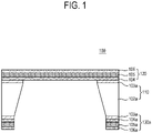
- FIG. 1 is a cross-section view of a pellicle for extreme ultraviolet (EUV) photomask according to a first embodiment of the present disclosure.
- EUV extreme ultraviolet
- a pellicle 100 for an EUV photomask includes a frame layer 110, and a pellicle layer 120 formed above the frame layer 110.
- the frame layer 110 includes an upper support layer pattern 102a and an upper etching stop layer pattern 103a.
- the pellicle layer 120 includes a lower reinforcing layer 104, a core layer 105 and an upper reinforcing layer 106.
- the support layer pattern 102a supports the pellicle layer 110, and facilitating easily handling and transferring when the pellicle is completely manufactured.
- the support layer pattern 102a is made of a material to be etched by a dry/wet etching process.
- the support layer pattern 102a may be formed by applying microfabrication technology to quartz, a silicon-on-insulator (SOI), or a silicon (Si) wafer.
- the support layer pattern 102a may be made of the silicon (Si) wafer that has a crystalline orientation of [100]; a doping density of 10 20 ions/cm 2 ; various sizes of 6 inch, 8 inch, etc.; and a thickness of 400 ⁇ m - 800 ⁇ m to be readily formed to have a desired shape when the support layer 102 of FIG. 3 is patterned by the wet etching process.
- the etching stop layer pattern 103a is buried between the support layer pattern 102a and the pellicle layer 120, and includes a silicon (Si) compound that contains one or more among carbon (C), nitrogen (N) and oxygen (O) in addition to silicon (Si) excellent in etching selectivity with the support layer 102 when the etching stop layer 103 of FIG. 3 is subjected to the dry/wet etching process.
- the etching stop layer pattern 102a is made of a material different from those of the lower reinforcing layer 104 and the core layer 105, and has a thickness of 10 - 500nm.
- the upper and lower reinforcing layers 104 and 106 are respectively formed on both surfaces of the core layer 105, or only one of the upper and lower reinforcing layers 104 and 106 may be formed on one side of the core layer 105.
- the upper and lower reinforcing layers 104 and 106 have high transmittance and protect the pellicle layer 120 from high temperature of the EUV process.
- the upper and lower reinforcing layers 104 and 106 include the silicon compound that contains one or more among carbon (C), nitrogen (N), oxygen (O) in addition to silicon (Si), or one or more materials among silicon carbide (SiC), boron carbide (B 4 C), ruthenium (Ru), molybdenum (Mo), graphene, a carbon nano tube (CNT), which are different in materials from those of the etching stop layer 102 and the core layer 105, and each has a thickness of 2-10nm.
- the upper and lower reinforcing layers 104 and 106 may be deteriorated in strength when they each has a thickness of 2nm or less, and may be remarkably decreased in transmittance of EUV exposure light and not usable when they each has a thickness of 10nm or more. Therefore, the upper and lower reinforcing layers 104 and 106 are formed to each has an optimum thickness in consideration of the overall transmittance and mechanical strength of the pellicle.
- the core layer 105 is materialized by a monocrystalline, amorphous or polycrystalline silicon layer excellent in transmittance, which may additionally contain one or more materials among boron (B), phosphorus (P), arsenic (As), yttrium (Y), zirconium (Zr), niobium (Nb) and molybdenum (Mo); or one or more metal silicide materials among molybdenum silicide (MoSi), tungsten silicide (WSi), zirconium silicide (ZrSi), tantalum silicide (TaSi), etc.
- B boron
- P phosphorus
- As arsenic
- Y yttrium
- Zr zirconium
- Nb zirconium
- Mo molybdenum
- MoSi molybdenum silicide
- WSi tungsten silicide
- ZrSi zirconium silicide
- TaSi tantalum sil
- the core layer 105 may be different in materials from the etching stop layer pattern 103a and the upper and lower reinforcing layers 104 and 106.
- the core layer 105 may have a thickness of 100 nm or less, and have a transmittance of 80% or higher with regard to the EUV exposure light having a wavelength of 13.5 nm.
- the EUV is well absorbed in any materials, and has strong thermal energy with a short wavelength. Therefore, it is very important to dissipate heat from the pellicle layer.
- a conventional method of solving a heat dissipation problem lays emphasis on finding a material having a good heat-dissipation coefficient.
- increase in a surface area is also taken into account in addition to selection of a material excellent in the heat-dissipation coefficient.
- a nano-pore is formed on the surface of the core layer 105 to thereby maximize the surface area and increase a heat-dissipation effect.
- the surface of the core layer 105 is subjected to surface treatment to complement the thermal characteristics of. the core layer 105. That is, the surface of the core layer 105 is formed with nano-sized fine pores, and thus an outer surface of the upper reinforcing layer 106 formed thereon is a porous surface. With this, the outer surface of the upper reinforcing layer 106 is increased in area, thereby increasing a heat-dissipation effect.
- the upper reinforcing layer 106 itself may be etched. However, in terms of the properties of the material, when the porous surface is formed by etching, it is more effective to etch the core layer 105 rather than the upper reinforcing layer 106.
- the surface has a roughness of 1-10 nm (see FIGS. 4 and 5 ).
- the surface of the reinforcing layer 106 also has the same roughness.
- the surface roughness ranges from 3 to 5nm.
- the surface roughness is of several nano meters, the surface of the layer has little influence on transmittance uniformity of the EUV light.
- the transmittance uniformity is deteriorated. That is, the surface roughness of 1-10 nm is preferable to increase the hight-dissipation effect while preventing light from scattering due to a nano structure.
- a lower thin-film layer pattern 130a including multi-layered patterns 103a, 104a, 105a, 106a is provided beneath the frame layer 110, and the lower thin-film layer pattern 130a is formed when the pellicle 100 of FIG. 1 is fabricated.
- FIG. 3 descriptions will be made with reference to FIG. 3 .
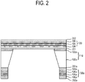
- FIG. 2 is a cross-section view of a pellicle for EUV lithography according to a second embodiment of the present disclosure. In this embodiment, detailed descriptions will be avoided and the same reference numerals will be given with regard to substantially the same elements as that of the embodiment illustrated in FIG. 1 .
- the pellicle for EUV lithography is the same as that of the foregoing first embodiment in light of including the frame layer 110 having the support layer pattern 102a and the etching stop layer pattern 103a, and the pellicle layer 120 having the frame layer 110, the lower reinforcing layer 104, the core layer 105 and the upper reinforcing layer 106.
- the pellicle according to this embodiment additionally includes auxiliary reinforcing layers 201 and 202 formed on both surfaces or either surface of the pellicle layer 120.
- the lower thin-film layer pattern 130a with multi-layered patterns 201a, 103a, 104a, 105a, 106a and 202a is provided beneath the frame layer 110.
- the lower thin-film layer pattern 130a is formed by processes similar to those of FIG. 3 (to be described) when the pellicle of FIG. 2 is fabricated, and thus detailed descriptions thereof will be avoided.
- the auxiliary reinforcing layers 201 and 202 includes a silicon (Si) compound that contains one or more among carbon (C), nitrogen (N) and oxygen (O) in addition to silicon (Si); or one or more materials among silicon carbide (SiC), boron carbide (B 4 C), ruthenium (Ru), molybdenum (Mo), graphene, and a carbon nano tube (CNT), which are different in material from the etching stop layer pattern 103a, the core layer 105 and the reinforcing layers 104 and 106, and each has a thickness of 2-10nm.
- Si silicon
- SiC silicon carbide
- B 4 C boron carbide
- Ru ruthenium
- Mo molybdenum
- CNT carbon nano tube
- the surface of the core layer 105 is subjected to surface treatment to improve thermal characteristics, and formed with nano-sized fine pores.
- the surface roughness may also range from 1 to 10 nm.
- the auxiliary reinforcing layer may be made of a metallic material to thereby improve heat-dissipation characteristics.
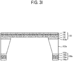
- FIGS. 3A to 31 are views of sequentially illustrating a method of fabricating the pellicle for the EUV lithography according to the first embodiment shown in FIG. 1 .
- the support layer 102 is prepared to be used as a base for fabricating the pellicle for the EUV photomask according to the present disclosure.
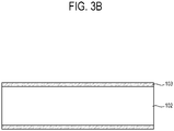
- the etching stop layer 103 including a silicon (Si) compound that contains one or more among oxygen (O), nitrogen (N) and carbon (C) in addition to silicon (Si) is formed on a top surface of the support layer 102 by chemical vapor deposition (CVD), a thermal oxidation process, sputtering, atomic layer deposition (ALD), etc.
- CVD chemical vapor deposition
- ALD atomic layer deposition
- the same layer as the etching stop layer 103 is formed on a bottom surface of the support layer 102.
- the etching stop layer 103 is made of a material having high etching selectivity with the support layer 102 for the etching process. Therefore, the etching selectivity may be equal to or higher than 104 so that the etching stop layer 103 can have a sufficient wet etching selectivity against the support layer 102. Further, the etching stop layer 103 may have the minimum residual stress to prevent the pellicle layer 120 from being broken while the pellicle is fabricated. Thus, the etching stop layer 103 is formed including silicon oxide having a compression stress lower than or equal to 300 Mpa.
- the lower reinforcing layer 104 is formed on the top surface of the upper etching stop layer 103 by CVD, sputtering, ALD, etc. In this case, the same layer as the lower reinforcing layer 104 is also formed on the bottom surface of the lower etching stop layer 103.
- the lower reinforcing layer 104 may be formed to have a tensile stress of 50-150 Mpa for an anti-wrinkle surface of the pellicle layer 120. Therefore, the lower reinforcing layer 104 according to the present disclosure may be made of silicon nitride excellent in not only mechanical strength and chemical durability but also step coverage.
- the core layer 105 is formed on the top surface of the upper lower reinforcing layer 104 by epitaxial growth, CVD, Sputtering, etc. In this case, the same layer as the core layer 105 is also formed on the bottom surface of the lower reinforcing layer 104.
- the core layer 105 may be made of polycrystalline silicon advantageous to a microfabrication process and excellent in optical, thermal and mechanical characteristics. Further, as described above, the surface of the core layer 105 is fabricated to have nano-sized porosity to improve thermal characteristics of the core layer 105. To form fine pores on the surface, a dry etching method and a wet etching method are possible. In this embodiment, the dry etching method may be used since the wet etching method is difficult to make the surface roughness be lower than or equal to 10 nm, and the higher roughness causes the transmittance uniformity to be decreased with regard to the EUV light.
- a nano-porous structure may be fabricated using XeF 2 gas of 25 sccm and N 2 gas of 100 sccm, and the process is performed for a short period of time of several seconds since polycrystalline silicon is quickly etched.
- the upper reinforcing layer 106 is deposited on the top surface of the upper core layer 105, and at the same time the same layer as the upper reinforcing layer 106 is formed on the bottom surface of the lower core layer 105.
- the upper reinforcing layer 106 is formed by the same method as that of forming the foregoing lower reinforcing layer 104.
- the etching mask layer 107 is formed on the outer surfaces of the upper reinforcing layers 106 on the upper side and the lower side by thermal oxidation process, CVD, sputtering, ALD., Etc.
- An etching mask layer 107 is made of a material having high etching selectivity against the support layer 102 and easily removable after etching the support layer 102, and includes a silicon compound that contains one or more among carbon (C), nitrogen (N) and oxygen (O) in addition to silicon (Si), or one or more materials among chrome, gold, aluminum and the like metal. According to the present disclosure, the etching mask layer 107 may use a silicon oxide film that is excellent in step coverage and thin-film density and causes relatively few or no surface defects. The etching mask layer 107 is formed to have at least a thickness of 100 nm in consideration of the process of etching the support layer 102 with regard to the whole thickness.
- the reinforcing layer 106 or the auxiliary reinforcing layer is partially etched and it may be thus difficult to accurately maintain the thickness.
- the etching mask layer 107 is laid on the top surface of the reinforcing layer 106 or the auxiliary reinforcing layer, thereby protecting the surfaces of the reinforcing layer and the auxiliary reinforcing layer and controlling the accurate thickness thereof.
- a photoresist film pattern 108a is formed on a bottom surface of a substrate, and the photoresist film pattern 108a is used as an etching mask to sequentially etch the etching mask layer 107, the upper reinforcing layer 106, the core layer 105, the lower reinforcing layer 104 and the etching stop layer 103 below the support layer 102 through the dry or wet etching process, thereby forming the lower thin-film layer pattern 130a through which the support layer 102 is exposed.
- the dry etching process resulting in a good etching profile is used.
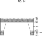
- the support layer 102 is etched by the dry etching process using a deep etcher, a XeF 2 etcher or the like, or by the wet etching process using potassium hydroxide (KOH), tetramethylammonium hydroxide (TMAH) or the like, thereby forming the support layer pattern 102a through which the etching stop layer 103 is exposed.
- KOH potassium hydroxide
- TMAH tetramethylammonium hydroxide
- TMAH having a very high etching selectivity of 104 or higher with the lower thin-film layer pattern 130a is used for etching the support layer 102.
- the etching stop layer 103 includes oxygen (O)
- the etching mask layer 107 may be made of a silicon compound that contains one or more among oxygen, carbon and nitrogen in addition to silicon.
- TMAH is used as an etchant more suitable for etching the support layer 102.
- a surfactant such as isopropyl alcohol (IPA), triton X-100, etc. may be added.
- the etching stop layer pattern 103a is formed to expose the lower reinforcing layer 104 through the dry or wet etching process, and the etching mask layer 107 is removed to thereby complete the fabrication of the pellicle for the EUV lithography according to an embodiment of the present disclosure.
- the etching mask layer 107 may be removed at the same time when the etching stop layer 103 is etched.
- the etching stop layer 103 and the etching mask layer 107 may be made of materials to be etched by the same etchant.
- etching mask layer 107 When the etching mask layer 107 is removed, an alkali etching solution remaining on the surface of the pellicle layer 130 is completely removed using desalted water, and then the etching stop layer 103 and the etching mask layer 107 are etched and removed.
- hydrogen fluoride HF may be used to etch and remove both the etching stop layer 103 and the etching mask layer 107.
- the etching stop layer 103 is provided between the support layer 102 and the pellicle layer 120, and therefore the pellicle layer 120 is prevented from being unintentionally damaged by an etchant for the support layer 102 when the support layer pattern 102a is etched by etching the support layer 102.
- the pellicle layer 120 or the lower reinforcing layer 104 or the lower auxiliary reinforcing layer 201 is very much thinner than the support layer 102 in the pellicle, and therefore these layers generally including SiN may be damaged by unintentional etching even though the etching selectivity is very high with regard to the support layer 102. Accordingly, it is possible to prevent such damage when the etching stop layer 103 is present according to the present disclosure.
- a pellicle for an EUV photomask which is excellent in mechanical strength and thermal conductivity while maintaining high transmittance for EUV exposure light with the minimum thickness.
Landscapes
- Physics & Mathematics (AREA)
- General Physics & Mathematics (AREA)
- Engineering & Computer Science (AREA)
- Health & Medical Sciences (AREA)
- Environmental & Geological Engineering (AREA)
- Epidemiology (AREA)
- Public Health (AREA)
- Plasma & Fusion (AREA)
- Preparing Plates And Mask In Photomechanical Process (AREA)
- Exposure And Positioning Against Photoresist Photosensitive Materials (AREA)
- Exposure Of Semiconductors, Excluding Electron Or Ion Beam Exposure (AREA)
Description
- The present disclosure relates to a pellicle for extreme ultraviolet (EUV) lithography and a method of fabricating the same, and more particularly to a pellicle for EUV lithography, which has high transmittance to EUV exposure light and is improved in mechanical strength, and a method of fabricating the same.
- Development of exposure technology called photolithography has made it possible for a semiconductor integrated circuit (IC) to have high integration. To form a finer circuit pattern on a wafer, resolution (also referred to as a limit of resolution) in exposure equipment has to become higher. When a fine pattern beyond the limit of resolution is transferred, there is a problem that a distorted image different from an original mask pattern is transferred because of light interference caused by diffraction and scattering.
- A currently commercialized exposure process employs exposure equipment using an ArF wavelength range of 193nm to perform a transfer process and form a fine pattern on a wafer, but is limited in terms of forming a fine pattern of 32nm or less. Accordingly, there have been developed various methods such as immersion lithography of using a liquid medium having a higher refractive index (e.g. 1.44) than air; double lithography of performing exposure twice; phase shift technology of shifting a phase of light by 180 degrees and causing a destructive interference with adjacent transmission light; optical phase correction of correcting a small size or rounded end of a designed pattern caused by the interference and diffraction of light; etc. However, the exposure technology using the ArF wavelength is not only difficult to get a finer circuit line width narrower than or equal to 32nm, but also increases production costs and process complexity. Therefore, extreme ultraviolet (EUV) photolithography technology, in which a wavelength of 13.5nm very shorter than the wavelength of 193nm is used for a main exposure wavelength, has attracted attention as the next-generation process.
- By the way, the lithography process employs a photomask as an original plate for patterning, and a pattern on the photomask is transferred to a wafer. In this case, if the photomask is attached with impurities such as particles, foreign materials, etc., the impurities may damage the pattern transferred after absorbing or reflecting the exposure light and thus causes performance or yield of the semiconductor device.
- To prevent the surface of the photomask from being attached with impurities, a method of attaching a pellicle to the photomask is being used. The pellicle is attached to the top surface of the photomask, and therefore dust or foreign materials on the pellicle are out of focus and not transferred to the pattern since the pattern of the photomask is in focus at a photolithography process even though impurities are attached to the pellicle. With recent fineness of the circuit line width, the size of impurities that may have an effect on the damage of the pattern is decreased, thereby increasing importance of the pellicle for protecting the photomask.
- When the pellicle is provided as a single film using a material having a low extinction coefficient with regard to EUV light of 13.5nm, it is easy to guarantee transmittance but very difficult to secure good mechanical and thermal characteristics. Accordingly, a multi-layered pellicle has been researched to complement the performance of the pellicle.
- The pellicle is configured to include a pellicle layer in the form of an extremely thin film basically having a thickness of 100nm or less for smooth and excellent transmittance of the EUV exposure light. The pellicle layer has to satisfy mechanical reliability with regard to vacuum environments and acceleration of a moving stage, and thermal reliability with regard to a long-term exposure process. Taking these conditions into account, the material and structure of the pellicle layer are determined.
- Document
KR101624078B1 - Document
US2016/147141A1 provides a pellicle which comprises a pellicle membrane having a refractive index (n) of 1.9-5.0 under light with a wavelength of 550 nm and a pellicle frame to which the pellicle membrane is bonded. -
WO 2017/036944A1 describes a membrane assembly for EUV lithography that comprises: a membrane formed from at least one membrane layer; and a border holding the membrane, the border formed from the border region of the planar substrate. -
US2014/370423A1 discloses an extreme ultraviolet (EUV) photolithography pellicle with at least 70% transmissivity to EUV, formed from a layer of semiconductor material applied to a substrate. - Accordingly, an aspect of one or more exemplary embodiments may provide a pellicle for an EUV photomask, which is excellent in transmittance with regard to EUV exposure light and mechanical strength.
- According to one embodiment of the present disclosure, a pellicle for extreme ultraviolet (EUV) lithography includes:
- a support layer pattern which is formed by etching a support layer;
- a pellicle layer which is formed on the support layer pattern; and
- an etching stop layer pattern which is formed between the support layer pattern and the pellicle layer and formed by etching an etching stop layer for stopping etching when the support layer is etched; and
- wherein the pellicle layer comprises a core layer, and one or more reinforcing layers formed on at least one among both surfaces of the core layer and different in material from the core layer;
- wherein the reinforcing layer comprises an outer porous surface having nano-sized pores.
- The core layer may include: one or more materials among boron (B), phosphorus (P), arsenic (As), yttrium (Y), zirconium (Zr), niobium (Nb) and molybdenum (Mo) in addition to a monocrystalline, amorphous or polycrystalline silicon layer; or one or more metal silicide materials among molybdenum silicide (MoSi), tungsten silicide (WSi), zirconium silicide (ZrSi) and tantalum silicide (TaSi).
- The core layer may have a thickness of 100 nm or less.
- The reinforcing layer may include: a silicon compound including one or more among carbon (C), nitrogen (N), oxygen (O) in addition to silicon (Si); or one or more materials among silicon carbide (SiC), boron carbide (B4C), ruthenium (Ru), molybdenum (Mo), graphene, and a carbon nano tube (CNT).
- The reinforcing layer may be different in material from the core layer and the etching stop layer pattern, and have a thickness of 2-10nm and a tensile stress of 50-150 MPa.
- The etching stop layer pattern may include a silicon compound including one or more among carbon (C), nitrogen (N), oxygen (O) in addition to silicon (Si). The etching stop layer pattern may have a thickness of 10 - 500nm. The etching stop layer pattern may include silicon oxide having a compression stress lower than or equal to 300 Mpa.
- The pellicle may further include an auxiliary reinforcing layer additionally formed on an outer surface of at least one reinforcing layer.
- The auxiliary reinforcing layer may include: a silicon compound including one or more among carbon (C), nitrogen (N), oxygen (O) in addition to silicon (Si); or one or more materials among silicon carbide (SiC), boron carbide (B4C), ruthenium (Ru), molybdenum (Mo), graphene, and a carbon nano tube (CNT).
- The auxiliary reinforcing layer may be different in material from the core layer and the reinforcing layer, and have a thickness of 2-10nm.
- When the etching stop layer includes oxygen (O), tetramethylammonium hydroxide (TMAH) may be used for etching the support layer to form the support layer pattern.
- The pellicle may further include an etching mask layer formed on an outer surface of the reinforcing layer, and including a silicon compound including oxygen (O) in addition to silicon (Si).
- The silicon compound of the etching mask layer may include at least one of carbon (c) and nitrogen (N), or one or more metal materials among chrome, gold and aluminum.
- The reinforcing layer includes an outer porous surface having nano-sized pores.
- The porous surface of the reinforcing layer may be formed by making the core layer have a porous surface.
- The porous surface of the core layer may be formed by dry etching, and the dry etching may be performed using XeF2 and N2 gas.
- The porous surface may have a roughness of 1-10 nm.
- The above and/or other aspects will become apparent and more readily appreciated from the following description of exemplary embodiments, taken in conjunction with the accompanying drawings, in which:
-
FIG. 1 is a cross-section view of a pellicle for extreme ultraviolet lithography according to a first embodiment of the present disclosure; -
FIG. 2 is a cross-section view of a pellicle for extreme ultraviolet lithography according to a second embodiment of the present disclosure; -
FIGS. 3A to 31 are views of sequentially illustrating a method of fabricating the pellicle for the extreme ultraviolet lithography according to the first embodiment shown inFIG. 1 ; -
FIG. 4 is a schematic view of illustrating that a nano core is formed in a core layer according to the first embodiment shown inFIG. 1 ; and -
FIG. 5 is a view of illustrating the nano core represented in a portion of the core layer inFIG. 4 . -
FIG. 1 is a cross-section view of a pellicle for extreme ultraviolet (EUV) photomask according to a first embodiment of the present disclosure. - Referring to
FIG. 1 , apellicle 100 for an EUV photomask includes aframe layer 110, and apellicle layer 120 formed above theframe layer 110. Theframe layer 110 includes an uppersupport layer pattern 102a and an upper etchingstop layer pattern 103a. Thepellicle layer 120 includes alower reinforcing layer 104, acore layer 105 and anupper reinforcing layer 106. - The
support layer pattern 102a supports thepellicle layer 110, and facilitating easily handling and transferring when the pellicle is completely manufactured. Thesupport layer pattern 102a is made of a material to be etched by a dry/wet etching process. For example, thesupport layer pattern 102a may be formed by applying microfabrication technology to quartz, a silicon-on-insulator (SOI), or a silicon (Si) wafer. - The
support layer pattern 102a may be made of the silicon (Si) wafer that has a crystalline orientation of [100]; a doping density of 1020 ions/cm2; various sizes of 6 inch, 8 inch, etc.; and a thickness of 400µm - 800 µm to be readily formed to have a desired shape when thesupport layer 102 ofFIG. 3 is patterned by the wet etching process. - The etching
stop layer pattern 103a is buried between thesupport layer pattern 102a and thepellicle layer 120, and includes a silicon (Si) compound that contains one or more among carbon (C), nitrogen (N) and oxygen (O) in addition to silicon (Si) excellent in etching selectivity with thesupport layer 102 when theetching stop layer 103 ofFIG. 3 is subjected to the dry/wet etching process. The etchingstop layer pattern 102a is made of a material different from those of the lower reinforcinglayer 104 and thecore layer 105, and has a thickness of 10 - 500nm. - As a layer for reinforcing the mechanical strength and thermal characteristics of the
core layer 105, the upper and lower reinforcinglayers core layer 105, or only one of the upper and lower reinforcinglayers core layer 105. The upper and lower reinforcinglayers pellicle layer 120 from high temperature of the EUV process. The upper and lower reinforcinglayers etching stop layer 102 and thecore layer 105, and each has a thickness of 2-10nm. - Here, the upper and lower reinforcing
layers layers - The
core layer 105 is materialized by a monocrystalline, amorphous or polycrystalline silicon layer excellent in transmittance, which may additionally contain one or more materials among boron (B), phosphorus (P), arsenic (As), yttrium (Y), zirconium (Zr), niobium (Nb) and molybdenum (Mo); or one or more metal silicide materials among molybdenum silicide (MoSi), tungsten silicide (WSi), zirconium silicide (ZrSi), tantalum silicide (TaSi), etc. Further, thecore layer 105 may be different in materials from the etchingstop layer pattern 103a and the upper and lower reinforcinglayers core layer 105 may have a thickness of 100 nm or less, and have a transmittance of 80% or higher with regard to the EUV exposure light having a wavelength of 13.5 nm. - The EUV is well absorbed in any materials, and has strong thermal energy with a short wavelength. Therefore, it is very important to dissipate heat from the pellicle layer. By the way, a conventional method of solving a heat dissipation problem lays emphasis on finding a material having a good heat-dissipation coefficient. However, according to the present disclosure, increase in a surface area is also taken into account in addition to selection of a material excellent in the heat-dissipation coefficient. To this end, a nano-pore is formed on the surface of the
core layer 105 to thereby maximize the surface area and increase a heat-dissipation effect. - That is, according to the present disclosure, the surface of the
core layer 105 is subjected to surface treatment to complement the thermal characteristics of. thecore layer 105. That is, the surface of thecore layer 105 is formed with nano-sized fine pores, and thus an outer surface of the upper reinforcinglayer 106 formed thereon is a porous surface. With this, the outer surface of the upper reinforcinglayer 106 is increased in area, thereby increasing a heat-dissipation effect. To make the upper reinforcinglayer 106 have the porous surface, the upper reinforcinglayer 106 itself may be etched. However, in terms of the properties of the material, when the porous surface is formed by etching, it is more effective to etch thecore layer 105 rather than the upper reinforcinglayer 106. - In this case, the surface has a roughness of 1-10 nm (see
FIGS. 4 and5 ). When the surface of thecore layer 105 has the foregoing roughness, the surface of the reinforcinglayer 106 also has the same roughness. Preferably, the surface roughness ranges from 3 to 5nm. When the surface roughness is of several nano meters, the surface of the layer has little influence on transmittance uniformity of the EUV light. When the surface roughness is higher than several nano meters, the transmittance uniformity is deteriorated. That is, the surface roughness of 1-10 nm is preferable to increase the hight-dissipation effect while preventing light from scattering due to a nano structure. - In this embodiment, a lower thin-
film layer pattern 130a includingmulti-layered patterns frame layer 110, and the lower thin-film layer pattern 130a is formed when thepellicle 100 ofFIG. 1 is fabricated. In this regard, descriptions will be made with reference toFIG. 3 . -
FIG. 2 is a cross-section view of a pellicle for EUV lithography according to a second embodiment of the present disclosure. In this embodiment, detailed descriptions will be avoided and the same reference numerals will be given with regard to substantially the same elements as that of the embodiment illustrated inFIG. 1 . - Referring to
FIG. 2 , the pellicle for EUV lithography according to the second embodiment of the present disclosure is the same as that of the foregoing first embodiment in light of including theframe layer 110 having thesupport layer pattern 102a and the etchingstop layer pattern 103a, and thepellicle layer 120 having theframe layer 110, the lower reinforcinglayer 104, thecore layer 105 and the upper reinforcinglayer 106. The pellicle according to this embodiment additionally includes auxiliary reinforcinglayers pellicle layer 120. - In this embodiment, the lower thin-
film layer pattern 130a withmulti-layered patterns frame layer 110. The lower thin-film layer pattern 130a is formed by processes similar to those ofFIG. 3 (to be described) when the pellicle ofFIG. 2 is fabricated, and thus detailed descriptions thereof will be avoided. - The auxiliary reinforcing
layers stop layer pattern 103a, thecore layer 105 and the reinforcinglayers - Like that of the first embodiment, the surface of the
core layer 105 is subjected to surface treatment to improve thermal characteristics, and formed with nano-sized fine pores. Likewise, the surface roughness may also range from 1 to 10 nm. - According to this embodiment, when the auxiliary reinforcing
layers -
FIGS. 3A to 31 are views of sequentially illustrating a method of fabricating the pellicle for the EUV lithography according to the first embodiment shown inFIG. 1 . - First, as shown in
FIG. 3A , thesupport layer 102 is prepared to be used as a base for fabricating the pellicle for the EUV photomask according to the present disclosure. - Referring to
FIG. 3B , theetching stop layer 103 including a silicon (Si) compound that contains one or more among oxygen (O), nitrogen (N) and carbon (C) in addition to silicon (Si) is formed on a top surface of thesupport layer 102 by chemical vapor deposition (CVD), a thermal oxidation process, sputtering, atomic layer deposition (ALD), etc. In this case, the same layer as theetching stop layer 103 is formed on a bottom surface of thesupport layer 102. - It is advantageous that the
etching stop layer 103 is made of a material having high etching selectivity with thesupport layer 102 for the etching process. Therefore, the etching selectivity may be equal to or higher than 104 so that theetching stop layer 103 can have a sufficient wet etching selectivity against thesupport layer 102. Further, theetching stop layer 103 may have the minimum residual stress to prevent thepellicle layer 120 from being broken while the pellicle is fabricated. Thus, theetching stop layer 103 is formed including silicon oxide having a compression stress lower than or equal to 300 Mpa. - Referring to
FIG. 3C , the lower reinforcinglayer 104 is formed on the top surface of the upperetching stop layer 103 by CVD, sputtering, ALD, etc. In this case, the same layer as the lower reinforcinglayer 104 is also formed on the bottom surface of the loweretching stop layer 103. - The lower reinforcing
layer 104 may be formed to have a tensile stress of 50-150 Mpa for an anti-wrinkle surface of thepellicle layer 120. Therefore, the lower reinforcinglayer 104 according to the present disclosure may be made of silicon nitride excellent in not only mechanical strength and chemical durability but also step coverage. - Referring to
FIG. 3D , thecore layer 105 is formed on the top surface of the upper lower reinforcinglayer 104 by epitaxial growth, CVD, Sputtering, etc. In this case, the same layer as thecore layer 105 is also formed on the bottom surface of the lower reinforcinglayer 104. - According to the present disclosure, the
core layer 105 may be made of polycrystalline silicon advantageous to a microfabrication process and excellent in optical, thermal and mechanical characteristics. Further, as described above, the surface of thecore layer 105 is fabricated to have nano-sized porosity to improve thermal characteristics of thecore layer 105. To form fine pores on the surface, a dry etching method and a wet etching method are possible. In this embodiment, the dry etching method may be used since the wet etching method is difficult to make the surface roughness be lower than or equal to 10 nm, and the higher roughness causes the transmittance uniformity to be decreased with regard to the EUV light. Preferably, a nano-porous structure may be fabricated using XeF2 gas of 25 sccm and N2 gas of 100 sccm, and the process is performed for a short period of time of several seconds since polycrystalline silicon is quickly etched. - Referring to
FIG. 3E , the upper reinforcinglayer 106 is deposited on the top surface of theupper core layer 105, and at the same time the same layer as the upper reinforcinglayer 106 is formed on the bottom surface of thelower core layer 105. In this case, the upper reinforcinglayer 106 is formed by the same method as that of forming the foregoing lower reinforcinglayer 104. - Referring to
FIG. 3F , theetching mask layer 107 is formed on the outer surfaces of the upper reinforcinglayers 106 on the upper side and the lower side by thermal oxidation process, CVD, sputtering, ALD., Etc. - An
etching mask layer 107 is made of a material having high etching selectivity against thesupport layer 102 and easily removable after etching thesupport layer 102, and includes a silicon compound that contains one or more among carbon (C), nitrogen (N) and oxygen (O) in addition to silicon (Si), or one or more materials among chrome, gold, aluminum and the like metal. According to the present disclosure, theetching mask layer 107 may use a silicon oxide film that is excellent in step coverage and thin-film density and causes relatively few or no surface defects. Theetching mask layer 107 is formed to have at least a thickness of 100 nm in consideration of the process of etching thesupport layer 102 with regard to the whole thickness. During the etching, the reinforcinglayer 106 or the auxiliary reinforcing layer is partially etched and it may be thus difficult to accurately maintain the thickness. To prevent this, theetching mask layer 107 is laid on the top surface of the reinforcinglayer 106 or the auxiliary reinforcing layer, thereby protecting the surfaces of the reinforcing layer and the auxiliary reinforcing layer and controlling the accurate thickness thereof. - Referring to
FIG. 3G , aphotoresist film pattern 108a is formed on a bottom surface of a substrate, and thephotoresist film pattern 108a is used as an etching mask to sequentially etch theetching mask layer 107, the upper reinforcinglayer 106, thecore layer 105, the lower reinforcinglayer 104 and theetching stop layer 103 below thesupport layer 102 through the dry or wet etching process, thereby forming the lower thin-film layer pattern 130a through which thesupport layer 102 is exposed. In this case, the dry etching process resulting in a good etching profile is used. - Referring to
FIG. 3H , after removing thephotoresist film pattern 108a, thesupport layer 102 is etched by the dry etching process using a deep etcher, a XeF2 etcher or the like, or by the wet etching process using potassium hydroxide (KOH), tetramethylammonium hydroxide (TMAH) or the like, thereby forming thesupport layer pattern 102a through which theetching stop layer 103 is exposed. - According to the present disclosure, TMAH having a very high etching selectivity of 104 or higher with the lower thin-
film layer pattern 130a is used for etching thesupport layer 102. Further, when theetching stop layer 103 includes oxygen (O), it is preferable that TMAH is used for etching thesupport layer 102. As described above, theetching mask layer 107 may be made of a silicon compound that contains one or more among oxygen, carbon and nitrogen in addition to silicon. In particular, when theetching mask layer 107 includes oxygen (O), TMAH is used as an etchant more suitable for etching thesupport layer 102. - By the way, to reduce the surface defects such as the roughness, hillocks and the like of the etched surface when the
support layer 102 is etched for forming thesupport layer pattern 102a, a surfactant such as isopropyl alcohol (IPA), triton X-100, etc. may be added. - Referring to
FIG. 31 , the etchingstop layer pattern 103a is formed to expose the lower reinforcinglayer 104 through the dry or wet etching process, and theetching mask layer 107 is removed to thereby complete the fabrication of the pellicle for the EUV lithography according to an embodiment of the present disclosure. Theetching mask layer 107 may be removed at the same time when theetching stop layer 103 is etched. To this end, theetching stop layer 103 and theetching mask layer 107 may be made of materials to be etched by the same etchant. - When the
etching mask layer 107 is removed, an alkali etching solution remaining on the surface of the pellicle layer 130 is completely removed using desalted water, and then theetching stop layer 103 and theetching mask layer 107 are etched and removed. In this embodiment, hydrogen fluoride (HF) may be used to etch and remove both theetching stop layer 103 and theetching mask layer 107. - According to the present disclosure, the
etching stop layer 103 is provided between thesupport layer 102 and thepellicle layer 120, and therefore thepellicle layer 120 is prevented from being unintentionally damaged by an etchant for thesupport layer 102 when thesupport layer pattern 102a is etched by etching thesupport layer 102. In particular, thepellicle layer 120 or the lower reinforcinglayer 104 or the lowerauxiliary reinforcing layer 201 is very much thinner than thesupport layer 102 in the pellicle, and therefore these layers generally including SiN may be damaged by unintentional etching even though the etching selectivity is very high with regard to thesupport layer 102. Accordingly, it is possible to prevent such damage when theetching stop layer 103 is present according to the present disclosure. - As described above, according to an exemplary embodiment of the present disclosure, it is possible to provide a pellicle for an EUV photomask, which is excellent in mechanical strength and thermal conductivity while maintaining high transmittance for EUV exposure light with the minimum thickness.
- Although a few exemplary embodiments of the present disclosure have been shown and described in details with reference to the accompanying drawings, the embodiments are given for only illustrative purposes without limiting the meaning and scope of the present disclosure defined in the appended claims. Therefore, it will be appreciated by a person having an ordinary skill in the art that various changes and equivalents may be made in these exemplary embodiments. Thus, the scope of the present disclosure has to be defined by technical matters of the appended claims.
Claims (18)
- A pellicle (100) for extreme ultraviolet (EUV) lithography, the pellicle (100) comprising:a support layer pattern (102a) which is formed by etching a support layer;a pellicle layer (120) which is formed on the support layer pattern (102a); andan etching stop layer pattern (103a) which is formed between the support layer pattern (102a) and the pellicle layer (120) and formed by etching an etching stop layer for stopping etching when the support layer is etched; andwherein the pellicle layer (120) comprises a core layer (105), and one or more reinforcing layers (104,106) formed on at least one among both surfaces of the core layer (105) and different in material from the core layer (105);characterized in that the reinforcing layer (104, 106) comprises an outer porous surface having nano-sized pores.
- The pellicle (100) according to claim 1, wherein the core layer (105) comprises:one or more materials among boron (B), phosphorus (P), arsenic (As), yttrium (Y), zirconium (Zr), niobium (Nb) and molybdenum (Mo) in addition to a monocrystalline, amorphous or polycrystalline silicon layer; orone or more metal silicide materials among molybdenum silicide (MoSi), tungsten silicide (WSi), zirconium silicide (ZrSi) and tantalum silicide (TaSi).
- The pellicle (100) according to claim 1 or 2, wherein the core layer (105) has a thickness of 100 nm or less.
- The pellicle (100) according to any one of claims 1 to 3, wherein the reinforcing layer (104,106) comprises:a silicon compound comprising one or more among carbon (C), nitrogen (N), oxygen (O) in addition to silicon (Si); orone or more materials among silicon carbide (SiC), boron carbide (B4C), ruthenium (Ru), molybdenum (Mo), graphene, and a carbon nano tube (CNT).
- The pellicle (100) according to any one of claims 1 to 4, wherein the reinforcing layer (104,106) is different in material from the core layer (105) and the etching stop layer pattern (103a), and has a thickness of 2-10nm.
- The pellicle (100) according to any one of claims 1 to 5, wherein the reinforcing layer (104,106) has a tensile stress of 50-150 MPa.
- The pellicle (100) according to any one of claims 1 to 6, wherein the etching stop layer pattern (103a) comprises a silicon compound comprising one or more among carbon (C), nitrogen (N), oxygen (O) in addition to silicon (Si)
- The pellicle (100) according to any one of claims 1 to 7, wherein the etching stop layer pattern (103a) has a thickness of 10 - 500nm.
- The pellicle (100) according to any one of claims 1 to 8, wherein the etching stop layer pattern (103a) comprises silicon oxide having a compression stress lower than or equal to 300 Mpa.
- The pellicle (100) according to any one of claims 1 to 9, further comprising an auxiliary reinforcing layer (201, 202) additionally formed on an outer surface of at least one reinforcing layer.
- The pellicle (100) according to claim 10, wherein the auxiliary reinforcing layer (201, 202) comprises:a silicon compound comprising one or more among carbon (C), nitrogen (N), oxygen (O) in addition to silicon (Si); orone or more materials among silicon carbide (SiC), boron carbide (B4C), ruthenium (Ru), molybdenum (Mo), graphene, and a carbon nano tube (CNT).
- The pellicle (100) according to claim 10 or 11, wherein the auxiliary reinforcing layer (201, 202) is different in material from the core layer (105) and the reinforcing layer (104,106), and has a thickness of 2-10nm.
- The pellicle (100) according to any one of claims 1 to 12, wherein, when the etching stop layer comprises oxygen (O), the support layer pattern (102a) is formed by etching the support layer using tetramethylammonium hydroxide (TMAH).
- The pellicle (100) according to claim 13, further comprising an etching mask layer (107) formed on an outer surface of the reinforcing layer (104, 106), and comprising a silicon compound comprising oxygen (O) in addition to silicon (Si).
- The pellicle (100) according to claim 14, wherein the silicon compound of the etching mask layer (107) comprises at least one of carbon (c) and nitrogen (N), or one or more metal materials among chrome, gold and aluminum.
- The pellicle (100) according to any of claims 1 to 15, wherein the porous surface of the reinforcing layer (104, 106) is formed by making the core layer (105) have a porous surface.
- The pellicle (100) according to claim 16, wherein the porous surface of the core layer (105) is formed by dry etching.
- The pellicle (100) according to claim 17, wherein the dry etching is performed using XeF2 and N2 gas.
Applications Claiming Priority (1)
| Application Number | Priority Date | Filing Date | Title |
|---|---|---|---|
| KR1020170149847A KR101900720B1 (en) | 2017-11-10 | 2017-11-10 | Pellicle for Extreme Ultraviolet(EUV) Lithography and Method for fabricating the same |
Publications (2)
| Publication Number | Publication Date |
|---|---|
| EP3483656A1 EP3483656A1 (en) | 2019-05-15 |
| EP3483656B1 true EP3483656B1 (en) | 2022-11-30 |
Family
ID=61868405
Family Applications (1)
| Application Number | Title | Priority Date | Filing Date |
|---|---|---|---|
| EP18165360.1A Active EP3483656B1 (en) | 2017-11-10 | 2018-04-02 | Pellicle for euv lithography |
Country Status (6)
| Country | Link |
|---|---|
| US (1) | US10859901B2 (en) |
| EP (1) | EP3483656B1 (en) |
| JP (1) | JP6730364B2 (en) |
| KR (1) | KR101900720B1 (en) |
| CN (1) | CN109765752B (en) |
| TW (1) | TWI682856B (en) |
Families Citing this family (31)
| Publication number | Priority date | Publication date | Assignee | Title |
|---|---|---|---|---|
| US11016383B2 (en) | 2018-08-31 | 2021-05-25 | Taiwan Semiconductor Manufacturing Co., Ltd. | Pellicle for an EUV lithography mask and a method of manufacturing thereof |
| NL2024075B1 (en) * | 2018-11-16 | 2020-08-19 | Asml Netherlands Bv | A pellicle for euv lithography |
| EP3764163B1 (en) * | 2019-07-11 | 2023-04-12 | IMEC vzw | An extreme ultraviolet lithography device |
| CN114174919B (en) * | 2019-07-30 | 2025-09-30 | Asml荷兰有限公司 | Membrane diaphragm |
| KR102242341B1 (en) * | 2019-08-05 | 2021-04-20 | 주식회사 에프에스티 | Manufacturing method for A Pellicle frame and Manufacturing apparatus for the Pellicle |
| TWI743565B (en) * | 2019-09-24 | 2021-10-21 | 美商微相科技股份有限公司 | Method for detecting surface of photomask used in EUV lithography process and photomask component thereof |
| EP3798728A1 (en) * | 2019-09-26 | 2021-03-31 | S&S Tech Co., Ltd. | Pellicle for euv lithography and method for manufacturing the same |
| KR102273266B1 (en) * | 2019-10-23 | 2021-07-06 | 주식회사 에프에스티 | Manufacturing method for a Pellicle including integrated frame and membrane |
| EP3842861B1 (en) * | 2019-12-23 | 2025-03-12 | IMEC vzw | A method for forming an euvl pellicle |
| NL2027098B1 (en) * | 2020-01-16 | 2021-10-14 | Asml Netherlands Bv | Pellicle membrane for a lithographic apparatus |
| KR20220137023A (en) * | 2020-02-04 | 2022-10-11 | 신에쓰 가가꾸 고교 가부시끼가이샤 | A pellicle frame, a pellicle, an exposure master plate with a pellicle and an exposure method, and a method for manufacturing a semiconductor device or a liquid crystal display panel |
| CN113253566B (en) * | 2020-02-10 | 2024-04-09 | 永恒光实业股份有限公司 | Composite fine mask |
| US11194246B1 (en) | 2020-03-27 | 2021-12-07 | Intel Corporation | Monolithically framed pellicle membrane suitable for lithography in the fabrication of integrated circuits |
| KR102514088B1 (en) * | 2020-08-04 | 2023-03-27 | 주식회사 에스앤에스텍 | Pellicle Using 1-dimensinal Materials for Extreme Ultraviolet(EUV) Lithography and Method for Fabricating of the same |
| KR20220017137A (en) * | 2020-08-04 | 2022-02-11 | 주식회사 에스앤에스텍 | Pellicle for Extreme Ultraviolet(EUV) Lithography and Method for Fabricating of the same |
| US11392024B2 (en) | 2020-11-13 | 2022-07-19 | Taiwan Semiconductor Manufacturing Company, Ltd. | Photomask assembly and method of forming the same |
| KR102546968B1 (en) * | 2020-11-19 | 2023-06-23 | 주식회사 에프에스티 | Method for Fabricating Pellicle for EUV(extreme ultraviolet) Lithography |
| KR102668456B1 (en) * | 2020-12-07 | 2024-05-23 | 주식회사 에프에스티 | Pellicle Frame for EUV(extreme ultraviolet) Lithography |
| KR102694331B1 (en) * | 2021-04-12 | 2024-08-13 | 한국전자기술연구원 | Pellicle for extreme ultraviolet lithography based on yttrium |
| JP2024529666A (en) * | 2021-08-26 | 2024-08-08 | エーエスエムエル ネザーランズ ビー.ブイ. | Pellicle Membrane |
| US12066755B2 (en) * | 2021-08-27 | 2024-08-20 | Taiwan Semiconductor Manufacturing Company, Ltd. | Pellicle for an EUV lithography mask and a method of manufacturing thereof |
| KR20230033407A (en) | 2021-09-01 | 2023-03-08 | 삼성전자주식회사 | A reticle and method of forming patterns in a semiconductor device |
| KR102694334B1 (en) | 2021-10-18 | 2024-08-13 | 한국전자기술연구원 | Method for manufacturing free-standing nanomembrane using assist layer |
| KR20240110068A (en) | 2021-12-02 | 2024-07-12 | 엔테그리스, 아이엔씨. | Pellicles containing silicon carbide nanostructures and related devices and methods |
| WO2023112330A1 (en) * | 2021-12-17 | 2023-06-22 | 日本碍子株式会社 | Si membrane structure used to produce pellicle, and method for producing pellicle |
| EP4318128A1 (en) * | 2022-07-28 | 2024-02-07 | S&S Tech Co., Ltd. | Pellicle for euv lithography |
| KR102828040B1 (en) * | 2022-07-28 | 2025-07-04 | 주식회사 에스앤에스텍 | Pellicle for EUV Lithography |
| KR20240061663A (en) | 2022-11-01 | 2024-05-08 | 한국과학기술원 | Normal temperature process for protecting the capping layer when manufacturing EUV pellicle and EUV pellicle manufactured thereby |
| CN120883131A (en) * | 2023-03-28 | 2025-10-31 | 琳得科株式会社 | Method for manufacturing protective membrane components, protective membrane supports, and protective membrane components |
| CN120883132A (en) * | 2023-03-28 | 2025-10-31 | 琳得科株式会社 | Protective film assembly and method for manufacturing protective film assembly |
| CN121399541A (en) * | 2023-06-27 | 2026-01-23 | Asml荷兰有限公司 | Surface membrane, diaphragm, and manufacturing method thereof |
Family Cites Families (21)
| Publication number | Priority date | Publication date | Assignee | Title |
|---|---|---|---|---|
| US6927146B2 (en) * | 2003-06-17 | 2005-08-09 | Intel Corporation | Chemical thinning of epitaxial silicon layer over buried oxide |
| EP2051139B1 (en) | 2007-10-18 | 2010-11-24 | Shin-Etsu Chemical Co., Ltd. | Pellicle and method for manufacturing the same |
| JP4928494B2 (en) | 2008-05-02 | 2012-05-09 | 信越化学工業株式会社 | Pellicle and method for manufacturing pellicle |
| JP4934099B2 (en) | 2008-05-22 | 2012-05-16 | 信越化学工業株式会社 | Pellicle and method for manufacturing pellicle |
| JP5394808B2 (en) * | 2009-04-22 | 2014-01-22 | 信越化学工業株式会社 | Pellicle for lithography and method for manufacturing the same |
| JP2012151158A (en) | 2011-01-17 | 2012-08-09 | Shin Etsu Chem Co Ltd | Pellicle film for euv and pellicle, and method of producing pellicle film |
| WO2013152921A1 (en) * | 2012-04-12 | 2013-10-17 | Asml Netherlands B.V. | Pellicle, reticle assembly and lithographic apparatus |
| KR101699655B1 (en) * | 2013-03-15 | 2017-01-24 | 아사히 가세이 이-매터리얼즈 가부시키가이샤 | Pellicle film, and pellicle |
| JP2014211474A (en) * | 2013-04-17 | 2014-11-13 | 凸版印刷株式会社 | Pellicle and pellicle production method |
| CN105229776B (en) * | 2013-05-24 | 2019-05-03 | 三井化学株式会社 | Pellicle assembly and EUV exposure device containing the same |
| US9057957B2 (en) * | 2013-06-13 | 2015-06-16 | International Business Machines Corporation | Extreme ultraviolet (EUV) radiation pellicle formation method |
| TWI658321B (en) * | 2013-12-05 | 2019-05-01 | 荷蘭商Asml荷蘭公司 | Apparatus and method for manufacturing a pellicle, and a pellicle |
| KR101680937B1 (en) * | 2014-04-17 | 2016-11-30 | 한양대학교 산학협력단 | Pellicle for EUV Lithography and method of fabricating the same |
| KR20160002332A (en) * | 2014-06-30 | 2016-01-07 | 주식회사 에스앤에스텍 | Blankmask for Extreme Ultra-Violet Lithography and Photomask using the same |
| KR102233579B1 (en) | 2014-08-12 | 2021-03-30 | 삼성전자주식회사 | Pellicle for an extreme ultraviolet(euv) lithography |
| KR101624078B1 (en) * | 2015-04-24 | 2016-05-25 | 한양대학교 에리카산학협력단 | Pellicle and method of fabricating the same |
| KR102366806B1 (en) | 2015-05-13 | 2022-02-23 | 삼성전자주식회사 | Pellicle preventing a thermal accumulation and Extremely Ultra-Violet lithography apparatus having the same |
| CN118915394A (en) * | 2015-07-17 | 2024-11-08 | Asml荷兰有限公司 | Method for manufacturing a diaphragm assembly |
| KR102345543B1 (en) | 2015-08-03 | 2021-12-30 | 삼성전자주식회사 | Pellicle and photomask assembly including the same |
| KR102823373B1 (en) * | 2015-09-02 | 2025-06-20 | 에이에스엠엘 네델란즈 비.브이. | Method for manufacturing a membrane assembly |
| US9835940B2 (en) * | 2015-09-18 | 2017-12-05 | Taiwan Semiconductor Manufacturing Company, Ltd. | Method to fabricate mask-pellicle system |
-
2017
- 2017-11-10 KR KR1020170149847A patent/KR101900720B1/en active Active
-
2018
- 2018-04-02 EP EP18165360.1A patent/EP3483656B1/en active Active
- 2018-04-16 JP JP2018078063A patent/JP6730364B2/en active Active
- 2018-05-10 TW TW107115836A patent/TWI682856B/en active
- 2018-05-25 CN CN201810511606.XA patent/CN109765752B/en active Active
- 2018-08-24 US US16/111,381 patent/US10859901B2/en active Active
Also Published As
| Publication number | Publication date |
|---|---|
| TW201918372A (en) | 2019-05-16 |
| CN109765752A (en) | 2019-05-17 |
| CN109765752B (en) | 2022-08-09 |
| KR101900720B1 (en) | 2018-09-20 |
| US10859901B2 (en) | 2020-12-08 |
| US20190146324A1 (en) | 2019-05-16 |
| TWI682856B (en) | 2020-01-21 |
| JP6730364B2 (en) | 2020-07-29 |
| EP3483656A1 (en) | 2019-05-15 |
| JP2019091001A (en) | 2019-06-13 |
Similar Documents
| Publication | Publication Date | Title |
|---|---|---|
| US10859901B2 (en) | Pellicle for EUV lithography and method of fabricating the same | |
| KR101981950B1 (en) | Pellicle for Extreme Ultraviolet Lithography | |
| US10768523B2 (en) | Pellicle for EUV lithography and method of fabricating the same | |
| KR20190053766A (en) | Pellicle for Extreme Ultraviolet(EUV) Lithography and Method for fabricating the same | |
| TWI398723B (en) | Pellicle and method of manufacturing pellicle | |
| KR20190107603A (en) | Pellicle for Extreme Ultraviolet(EUV) Lithography and Method for fabricating the same | |
| KR102015437B1 (en) | Pellicle for an Extreme Ultraviolet(EUV) Lithography and method for fabricating the same | |
| KR20200126216A (en) | Pellicle for Extreme Ultraviolet(EUV) Lithography and method for fabricating of the same | |
| TWI785417B (en) | Pellicle for extreme ultraviolet lithography | |
| US20210096458A1 (en) | Pellicle for euv lithography and method for manufacturing the same | |
| CN106997847A (en) | Pellicle and method for producing the same | |
| KR20190141986A (en) | Pellicle for Extreme Ultraviolet(EUV) Lithography and Method for fabricating the same | |
| KR20190115681A (en) | Pellicle for Extreme Ultraviolet(EUV) Lithography and Method for fabricating the same | |
| KR20170126265A (en) | Pellicle for an Extreme Ultraviolet(EUV) Lithography and method for fabricating the same | |
| KR20220139656A (en) | A pellicle for extreme ultraviolet lithography including an amorphous carbon and a method for manufacturing the same | |
| KR20180029384A (en) | Pellicle for an Extreme Ultraviolet(EUV) Lithography and method for fabricating the same | |
| KR20200084206A (en) | Pellicle for Extreme Ultraviolet(EUV) Lithography and Method for fabricating the same | |
| TW202112547A (en) | Pellicle for euv lithography and method for manufacturing the same | |
| KR102546968B1 (en) | Method for Fabricating Pellicle for EUV(extreme ultraviolet) Lithography | |
| KR20190107604A (en) | Pellicle for Extreme Ultraviolet(EUV) Lithography and Method for fabricating the same | |
| US6528215B1 (en) | Substrate for diamond stencil mask and method for forming | |
| KR20240092300A (en) | Method for manufacturing EUV pellicle membrane | |
| CN107792849A (en) | Method for forming graphene layer | |
| CN107797378A (en) | Method for forming graphene layer | |
| JP2000182944A (en) | Method of manufacturing mask for X-ray exposure |
Legal Events
| Date | Code | Title | Description |
|---|---|---|---|
| PUAI | Public reference made under article 153(3) epc to a published international application that has entered the european phase |
Free format text: ORIGINAL CODE: 0009012 |
|
| STAA | Information on the status of an ep patent application or granted ep patent |
Free format text: STATUS: THE APPLICATION HAS BEEN PUBLISHED |
|
| AK | Designated contracting states |
Kind code of ref document: A1 Designated state(s): AL AT BE BG CH CY CZ DE DK EE ES FI FR GB GR HR HU IE IS IT LI LT LU LV MC MK MT NL NO PL PT RO RS SE SI SK SM TR |
|
| AX | Request for extension of the european patent |
Extension state: BA ME |
|
| STAA | Information on the status of an ep patent application or granted ep patent |
Free format text: STATUS: REQUEST FOR EXAMINATION WAS MADE |
|
| 17P | Request for examination filed |
Effective date: 20191115 |
|
| RBV | Designated contracting states (corrected) |
Designated state(s): AL AT BE BG CH CY CZ DE DK EE ES FI FR GB GR HR HU IE IS IT LI LT LU LV MC MK MT NL NO PL PT RO RS SE SI SK SM TR |
|
| GRAP | Despatch of communication of intention to grant a patent |
Free format text: ORIGINAL CODE: EPIDOSNIGR1 |
|
| STAA | Information on the status of an ep patent application or granted ep patent |
Free format text: STATUS: GRANT OF PATENT IS INTENDED |
|
| INTG | Intention to grant announced |
Effective date: 20220407 |
|
| GRAJ | Information related to disapproval of communication of intention to grant by the applicant or resumption of examination proceedings by the epo deleted |
Free format text: ORIGINAL CODE: EPIDOSDIGR1 |
|
| STAA | Information on the status of an ep patent application or granted ep patent |
Free format text: STATUS: REQUEST FOR EXAMINATION WAS MADE |
|
| INTC | Intention to grant announced (deleted) | ||
| GRAP | Despatch of communication of intention to grant a patent |
Free format text: ORIGINAL CODE: EPIDOSNIGR1 |
|
| STAA | Information on the status of an ep patent application or granted ep patent |
Free format text: STATUS: GRANT OF PATENT IS INTENDED |
|
| INTG | Intention to grant announced |
Effective date: 20220916 |
|
| GRAS | Grant fee paid |
Free format text: ORIGINAL CODE: EPIDOSNIGR3 |
|
| GRAA | (expected) grant |
Free format text: ORIGINAL CODE: 0009210 |
|
| STAA | Information on the status of an ep patent application or granted ep patent |
Free format text: STATUS: THE PATENT HAS BEEN GRANTED |
|
| AK | Designated contracting states |
Kind code of ref document: B1 Designated state(s): AL AT BE BG CH CY CZ DE DK EE ES FI FR GB GR HR HU IE IS IT LI LT LU LV MC MK MT NL NO PL PT RO RS SE SI SK SM TR |
|
| REG | Reference to a national code |
Ref country code: CH Ref legal event code: EP Ref country code: GB Ref legal event code: FG4D |
|
| REG | Reference to a national code |
Ref country code: AT Ref legal event code: REF Ref document number: 1535125 Country of ref document: AT Kind code of ref document: T Effective date: 20221215 |
|
| REG | Reference to a national code |
Ref country code: IE Ref legal event code: FG4D |
|
| REG | Reference to a national code |
Ref country code: DE Ref legal event code: R096 Ref document number: 602018043536 Country of ref document: DE |
|
| REG | Reference to a national code |
Ref country code: LT Ref legal event code: MG9D |
|
| REG | Reference to a national code |
Ref country code: NL Ref legal event code: MP Effective date: 20221130 |
|
| PG25 | Lapsed in a contracting state [announced via postgrant information from national office to epo] |
Ref country code: SE Free format text: LAPSE BECAUSE OF FAILURE TO SUBMIT A TRANSLATION OF THE DESCRIPTION OR TO PAY THE FEE WITHIN THE PRESCRIBED TIME-LIMIT Effective date: 20221130 Ref country code: PT Free format text: LAPSE BECAUSE OF FAILURE TO SUBMIT A TRANSLATION OF THE DESCRIPTION OR TO PAY THE FEE WITHIN THE PRESCRIBED TIME-LIMIT Effective date: 20230331 Ref country code: NO Free format text: LAPSE BECAUSE OF FAILURE TO SUBMIT A TRANSLATION OF THE DESCRIPTION OR TO PAY THE FEE WITHIN THE PRESCRIBED TIME-LIMIT Effective date: 20230228 Ref country code: LT Free format text: LAPSE BECAUSE OF FAILURE TO SUBMIT A TRANSLATION OF THE DESCRIPTION OR TO PAY THE FEE WITHIN THE PRESCRIBED TIME-LIMIT Effective date: 20221130 Ref country code: FI Free format text: LAPSE BECAUSE OF FAILURE TO SUBMIT A TRANSLATION OF THE DESCRIPTION OR TO PAY THE FEE WITHIN THE PRESCRIBED TIME-LIMIT Effective date: 20221130 Ref country code: ES Free format text: LAPSE BECAUSE OF FAILURE TO SUBMIT A TRANSLATION OF THE DESCRIPTION OR TO PAY THE FEE WITHIN THE PRESCRIBED TIME-LIMIT Effective date: 20221130 |
|
| REG | Reference to a national code |
Ref country code: AT Ref legal event code: MK05 Ref document number: 1535125 Country of ref document: AT Kind code of ref document: T Effective date: 20221130 |
|
| PG25 | Lapsed in a contracting state [announced via postgrant information from national office to epo] |
Ref country code: RS Free format text: LAPSE BECAUSE OF FAILURE TO SUBMIT A TRANSLATION OF THE DESCRIPTION OR TO PAY THE FEE WITHIN THE PRESCRIBED TIME-LIMIT Effective date: 20221130 Ref country code: PL Free format text: LAPSE BECAUSE OF FAILURE TO SUBMIT A TRANSLATION OF THE DESCRIPTION OR TO PAY THE FEE WITHIN THE PRESCRIBED TIME-LIMIT Effective date: 20221130 Ref country code: LV Free format text: LAPSE BECAUSE OF FAILURE TO SUBMIT A TRANSLATION OF THE DESCRIPTION OR TO PAY THE FEE WITHIN THE PRESCRIBED TIME-LIMIT Effective date: 20221130 Ref country code: IS Free format text: LAPSE BECAUSE OF FAILURE TO SUBMIT A TRANSLATION OF THE DESCRIPTION OR TO PAY THE FEE WITHIN THE PRESCRIBED TIME-LIMIT Effective date: 20230330 Ref country code: HR Free format text: LAPSE BECAUSE OF FAILURE TO SUBMIT A TRANSLATION OF THE DESCRIPTION OR TO PAY THE FEE WITHIN THE PRESCRIBED TIME-LIMIT Effective date: 20221130 Ref country code: GR Free format text: LAPSE BECAUSE OF FAILURE TO SUBMIT A TRANSLATION OF THE DESCRIPTION OR TO PAY THE FEE WITHIN THE PRESCRIBED TIME-LIMIT Effective date: 20230301 |
|
| PG25 | Lapsed in a contracting state [announced via postgrant information from national office to epo] |
Ref country code: NL Free format text: LAPSE BECAUSE OF FAILURE TO SUBMIT A TRANSLATION OF THE DESCRIPTION OR TO PAY THE FEE WITHIN THE PRESCRIBED TIME-LIMIT Effective date: 20221130 |
|
| PG25 | Lapsed in a contracting state [announced via postgrant information from national office to epo] |
Ref country code: SM Free format text: LAPSE BECAUSE OF FAILURE TO SUBMIT A TRANSLATION OF THE DESCRIPTION OR TO PAY THE FEE WITHIN THE PRESCRIBED TIME-LIMIT Effective date: 20221130 Ref country code: RO Free format text: LAPSE BECAUSE OF FAILURE TO SUBMIT A TRANSLATION OF THE DESCRIPTION OR TO PAY THE FEE WITHIN THE PRESCRIBED TIME-LIMIT Effective date: 20221130 Ref country code: EE Free format text: LAPSE BECAUSE OF FAILURE TO SUBMIT A TRANSLATION OF THE DESCRIPTION OR TO PAY THE FEE WITHIN THE PRESCRIBED TIME-LIMIT Effective date: 20221130 Ref country code: DK Free format text: LAPSE BECAUSE OF FAILURE TO SUBMIT A TRANSLATION OF THE DESCRIPTION OR TO PAY THE FEE WITHIN THE PRESCRIBED TIME-LIMIT Effective date: 20221130 Ref country code: CZ Free format text: LAPSE BECAUSE OF FAILURE TO SUBMIT A TRANSLATION OF THE DESCRIPTION OR TO PAY THE FEE WITHIN THE PRESCRIBED TIME-LIMIT Effective date: 20221130 Ref country code: AT Free format text: LAPSE BECAUSE OF FAILURE TO SUBMIT A TRANSLATION OF THE DESCRIPTION OR TO PAY THE FEE WITHIN THE PRESCRIBED TIME-LIMIT Effective date: 20221130 |
|
| PG25 | Lapsed in a contracting state [announced via postgrant information from national office to epo] |
Ref country code: SK Free format text: LAPSE BECAUSE OF FAILURE TO SUBMIT A TRANSLATION OF THE DESCRIPTION OR TO PAY THE FEE WITHIN THE PRESCRIBED TIME-LIMIT Effective date: 20221130 Ref country code: AL Free format text: LAPSE BECAUSE OF FAILURE TO SUBMIT A TRANSLATION OF THE DESCRIPTION OR TO PAY THE FEE WITHIN THE PRESCRIBED TIME-LIMIT Effective date: 20221130 |
|
| REG | Reference to a national code |
Ref country code: DE Ref legal event code: R097 Ref document number: 602018043536 Country of ref document: DE |
|
| PLBE | No opposition filed within time limit |
Free format text: ORIGINAL CODE: 0009261 |
|
| STAA | Information on the status of an ep patent application or granted ep patent |
Free format text: STATUS: NO OPPOSITION FILED WITHIN TIME LIMIT |
|
| REG | Reference to a national code |
Ref country code: DE Ref legal event code: R119 Ref document number: 602018043536 Country of ref document: DE |
|
| 26N | No opposition filed |
Effective date: 20230831 |
|
| PG25 | Lapsed in a contracting state [announced via postgrant information from national office to epo] |
Ref country code: SI Free format text: LAPSE BECAUSE OF FAILURE TO SUBMIT A TRANSLATION OF THE DESCRIPTION OR TO PAY THE FEE WITHIN THE PRESCRIBED TIME-LIMIT Effective date: 20221130 |
|
| REG | Reference to a national code |
Ref country code: CH Ref legal event code: PL |
|
| GBPC | Gb: european patent ceased through non-payment of renewal fee |
Effective date: 20230402 |
|
| PG25 | Lapsed in a contracting state [announced via postgrant information from national office to epo] |
Ref country code: LU Free format text: LAPSE BECAUSE OF NON-PAYMENT OF DUE FEES Effective date: 20230402 |
|
| REG | Reference to a national code |
Ref country code: BE Ref legal event code: MM Effective date: 20230430 |
|
| PG25 | Lapsed in a contracting state [announced via postgrant information from national office to epo] |
Ref country code: MC Free format text: LAPSE BECAUSE OF FAILURE TO SUBMIT A TRANSLATION OF THE DESCRIPTION OR TO PAY THE FEE WITHIN THE PRESCRIBED TIME-LIMIT Effective date: 20221130 |
|
| PG25 | Lapsed in a contracting state [announced via postgrant information from national office to epo] |
Ref country code: GB Free format text: LAPSE BECAUSE OF NON-PAYMENT OF DUE FEES Effective date: 20230402 |
|
| PG25 | Lapsed in a contracting state [announced via postgrant information from national office to epo] |
Ref country code: MC Free format text: LAPSE BECAUSE OF FAILURE TO SUBMIT A TRANSLATION OF THE DESCRIPTION OR TO PAY THE FEE WITHIN THE PRESCRIBED TIME-LIMIT Effective date: 20221130 Ref country code: LI Free format text: LAPSE BECAUSE OF NON-PAYMENT OF DUE FEES Effective date: 20230430 Ref country code: GB Free format text: LAPSE BECAUSE OF NON-PAYMENT OF DUE FEES Effective date: 20230402 Ref country code: FR Free format text: LAPSE BECAUSE OF NON-PAYMENT OF DUE FEES Effective date: 20230430 Ref country code: DE Free format text: LAPSE BECAUSE OF NON-PAYMENT OF DUE FEES Effective date: 20231103 Ref country code: CH Free format text: LAPSE BECAUSE OF NON-PAYMENT OF DUE FEES Effective date: 20230430 |
|
| REG | Reference to a national code |
Ref country code: IE Ref legal event code: MM4A |
|
| PG25 | Lapsed in a contracting state [announced via postgrant information from national office to epo] |
Ref country code: BE Free format text: LAPSE BECAUSE OF NON-PAYMENT OF DUE FEES Effective date: 20230430 |
|
| PG25 | Lapsed in a contracting state [announced via postgrant information from national office to epo] |
Ref country code: IE Free format text: LAPSE BECAUSE OF NON-PAYMENT OF DUE FEES Effective date: 20230402 |
|
| PG25 | Lapsed in a contracting state [announced via postgrant information from national office to epo] |
Ref country code: IE Free format text: LAPSE BECAUSE OF NON-PAYMENT OF DUE FEES Effective date: 20230402 |
|
| PG25 | Lapsed in a contracting state [announced via postgrant information from national office to epo] |
Ref country code: IT Free format text: LAPSE BECAUSE OF FAILURE TO SUBMIT A TRANSLATION OF THE DESCRIPTION OR TO PAY THE FEE WITHIN THE PRESCRIBED TIME-LIMIT Effective date: 20221130 |
|
| PG25 | Lapsed in a contracting state [announced via postgrant information from national office to epo] |
Ref country code: BG Free format text: LAPSE BECAUSE OF FAILURE TO SUBMIT A TRANSLATION OF THE DESCRIPTION OR TO PAY THE FEE WITHIN THE PRESCRIBED TIME-LIMIT Effective date: 20221130 |
|
| PG25 | Lapsed in a contracting state [announced via postgrant information from national office to epo] |
Ref country code: BG Free format text: LAPSE BECAUSE OF FAILURE TO SUBMIT A TRANSLATION OF THE DESCRIPTION OR TO PAY THE FEE WITHIN THE PRESCRIBED TIME-LIMIT Effective date: 20221130 |
|
| PG25 | Lapsed in a contracting state [announced via postgrant information from national office to epo] |
Ref country code: CY Free format text: LAPSE BECAUSE OF FAILURE TO SUBMIT A TRANSLATION OF THE DESCRIPTION OR TO PAY THE FEE WITHIN THE PRESCRIBED TIME-LIMIT; INVALID AB INITIO Effective date: 20180402 |
|
| PG25 | Lapsed in a contracting state [announced via postgrant information from national office to epo] |
Ref country code: HU Free format text: LAPSE BECAUSE OF FAILURE TO SUBMIT A TRANSLATION OF THE DESCRIPTION OR TO PAY THE FEE WITHIN THE PRESCRIBED TIME-LIMIT; INVALID AB INITIO Effective date: 20180402 |
|
| PG25 | Lapsed in a contracting state [announced via postgrant information from national office to epo] |
Ref country code: TR Free format text: LAPSE BECAUSE OF FAILURE TO SUBMIT A TRANSLATION OF THE DESCRIPTION OR TO PAY THE FEE WITHIN THE PRESCRIBED TIME-LIMIT Effective date: 20221130 |