EP3482486B1 - System and method to determine a capacitance of a capacitor - Google Patents
System and method to determine a capacitance of a capacitor Download PDFInfo
- Publication number
- EP3482486B1 EP3482486B1 EP16738563.2A EP16738563A EP3482486B1 EP 3482486 B1 EP3482486 B1 EP 3482486B1 EP 16738563 A EP16738563 A EP 16738563A EP 3482486 B1 EP3482486 B1 EP 3482486B1
- Authority
- EP
- European Patent Office
- Prior art keywords
- power converter
- output
- output current
- slope
- current
- Prior art date
- Legal status (The legal status is an assumption and is not a legal conclusion. Google has not performed a legal analysis and makes no representation as to the accuracy of the status listed.)
- Active
Links
Images


Classifications
-
- H—ELECTRICITY
- H02—GENERATION; CONVERSION OR DISTRIBUTION OF ELECTRIC POWER
- H02M—APPARATUS FOR CONVERSION BETWEEN AC AND AC, BETWEEN AC AND DC, OR BETWEEN DC AND DC, AND FOR USE WITH MAINS OR SIMILAR POWER SUPPLY SYSTEMS; CONVERSION OF DC OR AC INPUT POWER INTO SURGE OUTPUT POWER; CONTROL OR REGULATION THEREOF
- H02M1/00—Details of apparatus for conversion
- H02M1/36—Means for starting or stopping converters
-
- G—PHYSICS
- G01—MEASURING; TESTING
- G01R—MEASURING ELECTRIC VARIABLES; MEASURING MAGNETIC VARIABLES
- G01R27/00—Arrangements for measuring resistance, reactance, impedance, or electric characteristics derived therefrom
- G01R27/02—Measuring real or complex resistance, reactance, impedance, or other two-pole characteristics derived therefrom, e.g. time constant
- G01R27/26—Measuring inductance or capacitance; Measuring quality factor, e.g. by using the resonance method; Measuring loss factor; Measuring dielectric constants ; Measuring impedance or related variables
- G01R27/2605—Measuring capacitance
-
- H—ELECTRICITY
- H02—GENERATION; CONVERSION OR DISTRIBUTION OF ELECTRIC POWER
- H02M—APPARATUS FOR CONVERSION BETWEEN AC AND AC, BETWEEN AC AND DC, OR BETWEEN DC AND DC, AND FOR USE WITH MAINS OR SIMILAR POWER SUPPLY SYSTEMS; CONVERSION OF DC OR AC INPUT POWER INTO SURGE OUTPUT POWER; CONTROL OR REGULATION THEREOF
- H02M1/00—Details of apparatus for conversion
- H02M1/32—Means for protecting converters other than automatic disconnection
-
- H—ELECTRICITY
- H02—GENERATION; CONVERSION OR DISTRIBUTION OF ELECTRIC POWER
- H02M—APPARATUS FOR CONVERSION BETWEEN AC AND AC, BETWEEN AC AND DC, OR BETWEEN DC AND DC, AND FOR USE WITH MAINS OR SIMILAR POWER SUPPLY SYSTEMS; CONVERSION OF DC OR AC INPUT POWER INTO SURGE OUTPUT POWER; CONTROL OR REGULATION THEREOF
- H02M3/00—Conversion of dc power input into dc power output
- H02M3/22—Conversion of dc power input into dc power output with intermediate conversion into ac
- H02M3/24—Conversion of dc power input into dc power output with intermediate conversion into ac by static converters
- H02M3/28—Conversion of dc power input into dc power output with intermediate conversion into ac by static converters using discharge tubes with control electrode or semiconductor devices with control electrode to produce the intermediate ac
- H02M3/325—Conversion of dc power input into dc power output with intermediate conversion into ac by static converters using discharge tubes with control electrode or semiconductor devices with control electrode to produce the intermediate ac using devices of a triode or a transistor type requiring continuous application of a control signal
- H02M3/335—Conversion of dc power input into dc power output with intermediate conversion into ac by static converters using discharge tubes with control electrode or semiconductor devices with control electrode to produce the intermediate ac using devices of a triode or a transistor type requiring continuous application of a control signal using semiconductor devices only
- H02M3/33569—Conversion of dc power input into dc power output with intermediate conversion into ac by static converters using discharge tubes with control electrode or semiconductor devices with control electrode to produce the intermediate ac using devices of a triode or a transistor type requiring continuous application of a control signal using semiconductor devices only having several active switching elements
- H02M3/33576—Conversion of dc power input into dc power output with intermediate conversion into ac by static converters using discharge tubes with control electrode or semiconductor devices with control electrode to produce the intermediate ac using devices of a triode or a transistor type requiring continuous application of a control signal using semiconductor devices only having several active switching elements having at least one active switching element at the secondary side of an isolation transformer
- H02M3/33592—Conversion of dc power input into dc power output with intermediate conversion into ac by static converters using discharge tubes with control electrode or semiconductor devices with control electrode to produce the intermediate ac using devices of a triode or a transistor type requiring continuous application of a control signal using semiconductor devices only having several active switching elements having at least one active switching element at the secondary side of an isolation transformer having a synchronous rectifier circuit or a synchronous freewheeling circuit at the secondary side of an isolation transformer
-
- G—PHYSICS
- G01—MEASURING; TESTING
- G01D—MEASURING NOT SPECIALLY ADAPTED FOR A SPECIFIC VARIABLE; ARRANGEMENTS FOR MEASURING TWO OR MORE VARIABLES NOT COVERED IN A SINGLE OTHER SUBCLASS; TARIFF METERING APPARATUS; MEASURING OR TESTING NOT OTHERWISE PROVIDED FOR
- G01D5/00—Mechanical means for transferring the output of a sensing member; Means for converting the output of a sensing member to another variable where the form or nature of the sensing member does not constrain the means for converting; Transducers not specially adapted for a specific variable
- G01D5/12—Mechanical means for transferring the output of a sensing member; Means for converting the output of a sensing member to another variable where the form or nature of the sensing member does not constrain the means for converting; Transducers not specially adapted for a specific variable using electric or magnetic means
- G01D5/14—Mechanical means for transferring the output of a sensing member; Means for converting the output of a sensing member to another variable where the form or nature of the sensing member does not constrain the means for converting; Transducers not specially adapted for a specific variable using electric or magnetic means influencing the magnitude of a current or voltage
- G01D5/24—Mechanical means for transferring the output of a sensing member; Means for converting the output of a sensing member to another variable where the form or nature of the sensing member does not constrain the means for converting; Transducers not specially adapted for a specific variable using electric or magnetic means influencing the magnitude of a current or voltage by varying capacitance
-
- G—PHYSICS
- G01—MEASURING; TESTING
- G01R—MEASURING ELECTRIC VARIABLES; MEASURING MAGNETIC VARIABLES
- G01R27/00—Arrangements for measuring resistance, reactance, impedance, or electric characteristics derived therefrom
- G01R27/02—Measuring real or complex resistance, reactance, impedance, or other two-pole characteristics derived therefrom, e.g. time constant
- G01R27/26—Measuring inductance or capacitance; Measuring quality factor, e.g. by using the resonance method; Measuring loss factor; Measuring dielectric constants ; Measuring impedance or related variables
-
- H—ELECTRICITY
- H02—GENERATION; CONVERSION OR DISTRIBUTION OF ELECTRIC POWER
- H02M—APPARATUS FOR CONVERSION BETWEEN AC AND AC, BETWEEN AC AND DC, OR BETWEEN DC AND DC, AND FOR USE WITH MAINS OR SIMILAR POWER SUPPLY SYSTEMS; CONVERSION OF DC OR AC INPUT POWER INTO SURGE OUTPUT POWER; CONTROL OR REGULATION THEREOF
- H02M3/00—Conversion of dc power input into dc power output
- H02M3/02—Conversion of dc power input into dc power output without intermediate conversion into ac
- H02M3/04—Conversion of dc power input into dc power output without intermediate conversion into ac by static converters
- H02M3/10—Conversion of dc power input into dc power output without intermediate conversion into ac by static converters using discharge tubes with control electrode or semiconductor devices with control electrode
- H02M3/145—Conversion of dc power input into dc power output without intermediate conversion into ac by static converters using discharge tubes with control electrode or semiconductor devices with control electrode using devices of a triode or transistor type requiring continuous application of a control signal
- H02M3/155—Conversion of dc power input into dc power output without intermediate conversion into ac by static converters using discharge tubes with control electrode or semiconductor devices with control electrode using devices of a triode or transistor type requiring continuous application of a control signal using semiconductor devices only
- H02M3/156—Conversion of dc power input into dc power output without intermediate conversion into ac by static converters using discharge tubes with control electrode or semiconductor devices with control electrode using devices of a triode or transistor type requiring continuous application of a control signal using semiconductor devices only with automatic control of output voltage or current, e.g. switching regulators
- H02M3/157—Conversion of dc power input into dc power output without intermediate conversion into ac by static converters using discharge tubes with control electrode or semiconductor devices with control electrode using devices of a triode or transistor type requiring continuous application of a control signal using semiconductor devices only with automatic control of output voltage or current, e.g. switching regulators with digital control
-
- H—ELECTRICITY
- H02—GENERATION; CONVERSION OR DISTRIBUTION OF ELECTRIC POWER
- H02M—APPARATUS FOR CONVERSION BETWEEN AC AND AC, BETWEEN AC AND DC, OR BETWEEN DC AND DC, AND FOR USE WITH MAINS OR SIMILAR POWER SUPPLY SYSTEMS; CONVERSION OF DC OR AC INPUT POWER INTO SURGE OUTPUT POWER; CONTROL OR REGULATION THEREOF
- H02M3/00—Conversion of dc power input into dc power output
- H02M3/22—Conversion of dc power input into dc power output with intermediate conversion into ac
- H02M3/24—Conversion of dc power input into dc power output with intermediate conversion into ac by static converters
- H02M3/28—Conversion of dc power input into dc power output with intermediate conversion into ac by static converters using discharge tubes with control electrode or semiconductor devices with control electrode to produce the intermediate ac
- H02M3/325—Conversion of dc power input into dc power output with intermediate conversion into ac by static converters using discharge tubes with control electrode or semiconductor devices with control electrode to produce the intermediate ac using devices of a triode or a transistor type requiring continuous application of a control signal
- H02M3/335—Conversion of dc power input into dc power output with intermediate conversion into ac by static converters using discharge tubes with control electrode or semiconductor devices with control electrode to produce the intermediate ac using devices of a triode or a transistor type requiring continuous application of a control signal using semiconductor devices only
- H02M3/33507—Conversion of dc power input into dc power output with intermediate conversion into ac by static converters using discharge tubes with control electrode or semiconductor devices with control electrode to produce the intermediate ac using devices of a triode or a transistor type requiring continuous application of a control signal using semiconductor devices only with automatic control of the output voltage or current, e.g. flyback converters
- H02M3/33515—Conversion of dc power input into dc power output with intermediate conversion into ac by static converters using discharge tubes with control electrode or semiconductor devices with control electrode to produce the intermediate ac using devices of a triode or a transistor type requiring continuous application of a control signal using semiconductor devices only with automatic control of the output voltage or current, e.g. flyback converters with digital control
-
- H—ELECTRICITY
- H02—GENERATION; CONVERSION OR DISTRIBUTION OF ELECTRIC POWER
- H02M—APPARATUS FOR CONVERSION BETWEEN AC AND AC, BETWEEN AC AND DC, OR BETWEEN DC AND DC, AND FOR USE WITH MAINS OR SIMILAR POWER SUPPLY SYSTEMS; CONVERSION OF DC OR AC INPUT POWER INTO SURGE OUTPUT POWER; CONTROL OR REGULATION THEREOF
- H02M3/00—Conversion of dc power input into dc power output
- H02M3/22—Conversion of dc power input into dc power output with intermediate conversion into ac
- H02M3/24—Conversion of dc power input into dc power output with intermediate conversion into ac by static converters
- H02M3/28—Conversion of dc power input into dc power output with intermediate conversion into ac by static converters using discharge tubes with control electrode or semiconductor devices with control electrode to produce the intermediate ac
- H02M3/325—Conversion of dc power input into dc power output with intermediate conversion into ac by static converters using discharge tubes with control electrode or semiconductor devices with control electrode to produce the intermediate ac using devices of a triode or a transistor type requiring continuous application of a control signal
- H02M3/335—Conversion of dc power input into dc power output with intermediate conversion into ac by static converters using discharge tubes with control electrode or semiconductor devices with control electrode to produce the intermediate ac using devices of a triode or a transistor type requiring continuous application of a control signal using semiconductor devices only
- H02M3/33569—Conversion of dc power input into dc power output with intermediate conversion into ac by static converters using discharge tubes with control electrode or semiconductor devices with control electrode to produce the intermediate ac using devices of a triode or a transistor type requiring continuous application of a control signal using semiconductor devices only having several active switching elements
- H02M3/33576—Conversion of dc power input into dc power output with intermediate conversion into ac by static converters using discharge tubes with control electrode or semiconductor devices with control electrode to produce the intermediate ac using devices of a triode or a transistor type requiring continuous application of a control signal using semiconductor devices only having several active switching elements having at least one active switching element at the secondary side of an isolation transformer
Definitions
- the present invention is directed, in general, to the field of power electronics and, more specifically, to a system and method to determine a capacitance of a capacitor.
- a switched-mode power converter is a type of power converter having a diverse range of applications by virtue of its small size, weight and high efficiency.
- switched-mode power converters are widely used in personal computers and portable electronic devices such as cellphones.
- a switching device e.g., a metal-oxide semiconductor field-effect transistor ("MOSFET")
- MOSFET metal-oxide semiconductor field-effect transistor
- a frequency and duty cycle of t e switching device is adjusted using a feedback signal to convert the input voltage to the desired output voltage.
- a feedback loop of the power converter that provides the feedback signal may be monitored and adjusted to enhance the regulation of the output characteristic such as the output voltage.
- Dynamic elements of the power converter such as inductors and capacitors can affect the feedback loop design parameters.
- a capacitance of an output capacitor is not only dependent on internal capacitances of the power converter, but also load capacitances that can vary from application to application.
- the feedback loop performance affects input and output currents produced by the power converter during startup-up as well as the ability to regulate the output characteristic in the presence of load transients.
- the inductors are generally included internally in the power converter design and, thus, provide known reactive values for the design of the feedback loop.
- the design of the feedback loop is dependent on load capacitances that are unknown or only partially known during the design phase.
- Technical developments over time have improved electrical characteristics of capacitors such that they can have a higher capacitance in a given physical size as well as a lower equivalent series resistance (“ESR"). That being said, the unknown load capacitances still can have a significant effect on feedback loop performance.
- ESR equivalent series resistance
- Related art within this technical field is disclosed, for e.g. D1: EP2704300A1, filed August 6, 2012 , entitled “Method for controlling a power stage”, describes a background art of method for controlling a DC-DC power converter.
- a power converter includes a controller coupled to an output capacitor and a power train configured to convert an input voltage to a nominal output voltage.
- the controller is configured to ramp up an output voltage of the power converter with a first slope and a second slope, and receive a first output current of the power converter during a first rise time associated with the first slope and a second output current of the power converter during a second rise time associated with the second slope.
- the controller is also configured to compute a capacitance of the output capacitor employing the first and second output currents, the first and second rise times, and the nominal output voltage.
- Corresponding embodiments are also applicable for a method of operating a power converter and a controller for use with a power converter.
- a process will be described herein with respect to exemplary embodiments in a specific context, namely, a system and method operable to identify a capacitance of an output capacitor of a power converter. While the principles will be described in the environment of a power converter, a motor controller, or power amplifier that may benefit from such a system and method that enables these functionalities is well within the broad scope of the present disclosure.
- system dynamic components such as an output capacitance should be properly identified.
- a common method in system identification is to superimpose a disturbance on an internal signal and analyze what happens on the output, for example, as described in " System Identification - Theory for the User” by L. Ljung (Prentice-Hall, Englewood Cliffs, ISBN 0-13-B81640, 1987 ).
- Such a disturbance can be injected in many different ways.
- One way is to use relay feedback, as described in " Automatic tuning of PID controllers” by K. J. ⁇ ström and T. Hägglund (Instrument Society of America, ISBN 1-55617-081-5, 1988 ).
- the disturbance can be injected by inducing limit cycles or injecting a noise signal, as described in the doctoral thesis of Zhao Zhenyu, entitled “Design and Practical Implementation of Digital Auto-tuning and Fast-response Controllers for Low-power Switch-mode Power Supplies” (University of Toronto, Canada, 2008 ).
- a problem with the above schemes is to control or limit an amplitude of the disturbance at the output of the power converter.
- the loads of the power converter sometimes have very strict requirements on overvoltage, which make such methods difficult to use.
- no disturbance at all on the output voltage can be tolerated.
- the aforementioned methods employing feedback control employ complex calculations that take time and consume power.
- these solutions place heavy demands on computational resources.
- Other methods that involve injecting sinusoidal disturbances and using cross-correlation to determine the system's transfer function are also time consuming and use complex calculations that take time and consume power, and employ a fair amount of computation resources.
- CMOS complementary metal-oxide semiconductor
- ASICs application specific integrated circuits
- FPGAs field programmable gate arrays
- ESR equivalent series resistance
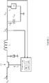
- FIGURE 1 illustrated is a schematic diagram of an embodiment of a power converter.
- the power converter receives an input voltage I in and converts a direct current (“dc") input voltage V in (from an input power source) to a desired dc output voltage V out .
- the output voltage V out is applied across a load (designated "LD") connected in parallel with an output capacitor Cout.
- An output current lout is split between the output capacitor Cout (receiving a capacitor current Ic) and the load LD (receiving a load current IL).
- the power converter includes an inductor L, the output capacitor C out , a diode D1 and a power switch 110.
- the power converter also includes a controller 130 (including a processor (“PR”) 140 and memory (“M”) 150) that controls the power switch 110 to regulate the output voltage V out of the power converter.
- PR processor
- M memory
- the controller 130 applies a control signal Cs at an appropriate frequency (e.g ., 300 kilohertz ("kHz")) to a control terminal of the power switch (also referred to as a "switching device") 110.
- the controller 130 is also configured to compute a capacitance of the output capacitor Cout of the power converter.
- the power converter may use large banks of capacitors for maintaining a stable output voltage V out during load transients or for keeping the voltage ripple at an acceptable level.
- the power converter illustrated in FIGURE 1 is not limited to the above-described buck topology, and the apparatus and methods introduced herein will work equally well with many topologies including push-pull, half-bridge and forward converters, etc. Further, it will be appreciated that the techniques of the solution introduced herein are applicable to various types of switched mode power supplies ( e.g ., dc-dc, etc ).
- the processor 140 may be embodied as any type of processor and associated circuitry configured to perform one or more of the functions described herein.
- the processor 140 may be embodied as or otherwise include a single or multicore processor, an application specific integrated circuit, a collection of logic devices, or other circuits.
- the memory 150 may be embodied as read-only memory devices and/or random access memory devices.
- the memory 150 may be embodied as or otherwise include dynamic random access memory devices ("DRAM"), synchronous dynamic random access memory devices (“SDRAM”), double-data rate dynamic random access memory devices (“DDR SDRAM”), and/or other volatile or non-volatile memory devices.
- the memory 150 may have stored therein programs including a plurality of instructions or computer program code for execution by the processor 140 to control particular functions of the power converter as discussed in more detail below.
- FIGURE 2 illustrated is a schematic diagram of another embodiment of a power converter.
- a power train of the power converter receives an input voltage I in and an input voltage V in and includes first and second high-side switching devices Q1, Q2, and first and second low-side switching devices Q3, Q4 arranged in a full bridge configuration and including parasitic capacitances (illustrated with dotted lines as parallel capacitances).
- the first high-side switching device Q1 is coupled in series at a first circuit node Va with the first low-side switching device Q3.
- the second high-side switching device Q2 is coupled in series at a second circuit node Vb with the second low-side switching device Q4.
- the first and second circuit nodes Va, Vb are coupled to opposite ends of a primary winding of a transformer TR.
- a secondary winding of the transformer TR is coupled to a synchronous rectifier formed by a third low-side switching device Q5 (including a parasitic capacitance, not shown) coupled to a fourth low-side switching device Q6 (including a parasitic capacitance, not shown).
- a center tap of the secondary winding of the transformer TR is coupled to an output filter including output inductor L and output capacitor Cout that filters an output voltage V out provided to a load (designated "LD").
- An output current lout is split between the output capacitor Cout (receiving a capacitor current Ic) and the load LD (receiving a load current IL).
- the first and second high-side switching devices Q1, Q2, and the first and second low-side switching devices Q3, Q4 are controlled to provide a high frequency ac voltage to the primary winding of the transformer TR.
- the high frequency ac voltage is impressed across to the secondary winding of the transformer TR and the third and fourth low-side switching devices Q5, Q6 are controlled to provide a rectified dc voltage.
- the rectified dc voltage is then filtered by the output filter, which provides the output voltage V out to the load LD.
- the switching devices are illustrated as MOSFETs, it should be understood that any semiconductor switch technology can be used as the application dictates.
- the power train includes a full bridge configuration and synchronous rectifier, other topologies and rectification techniques may be employed to advantage.
- a controller 210 including a processor (“PR”) 220 and memory (“M”) 230 receives the output current lout and/or the output voltage V out and generates control signals Cs1, Cs2, Cs3, Cs4 for the first and second high-side switching devices Q1, Q2, and first and second low-side switching devices Q3, Q4 to regulate the output voltage V out (an output characteristic of the power converter).
- the controller 210 also generates control signals Cs5, Cs6 for the synchronous rectifier formed by the third and fourth low-side switching devices Q5, Q6.
- a description of analogous controller 130 is described above with respect to FIGURE 1 .
- the controller 210 is also configured to compute a capacitance of the output capacitor Cout of the power converter.
- FIGURE 3 illustrated are timing diagrams demonstrating an operation of the power converter of FIGURE 2 .
- the timing diagrams represent the conduction intervals for the switching devices Q1, Q2, Q3, Q4, Q5, Q6 over a switching interval T as a function of time t (on the horizontal axis).
- the first high-side switching device Q1 and the second low-side switching device Q4 conduct for a duty cycle D delivering energy to the transformer TR.
- the fourth low-side switching device Q6 is also conducting during this time.
- the first and second high-side switching devices Q1, Q2, and the first and second low-side switching devices Q3, Q4 are non-conducting, and a current in the output inductor L flows through the third and fourth low-side switching devices Q5, Q6 of the synchronous rectifier.
- the second high-side switching device Q2 and the first low-side switching device Q3 conduct delivering energy to the transformer TR.
- the third low-side switching device Q5 is also conducting during this time.
- the first and second high-side switching devices Q1, Q2, and the first and second low-side switching devices Q3, Q4 are non-conducting, and a current in the output inductor L flows through the third and fourth low-side switching devices Q5, Q6 of the synchronous rectifier.
- FIGURE 4 illustrated are timing diagrams demonstrating an operation of a power converter.
- the illustrated embodiment demonstrates an output voltage V out and output current I out of the power converter as a function of time t at start-up.
- the output voltage V out , the output current lout and a rise time t r1 a set forth below are employed to compute a capacitance of an output capacitor Cout of the power converter (see, e.g., equation (9)).
- the output voltage V out is ramped up from an initial output voltage V start to a steady-state nominal output voltage (also referred to as a "nominal output voltage”) V nom .
- a steady-state nominal output voltage also referred to as a "nominal output voltage
- the power train starts with a minimum duty cycle D min and the output voltage V out makes a quick jump to the initial output voltage V start at a time t d , which may include a configurable delay after a remote control signal starts the ramp-up sequence.
- the initial output voltage V start equals n•D min •V in , wherein "n" is a transformer turns ratio for power converters that include an isolation transformer. Otherwise, the transformer turns ratio n is set to one.
- This jump in duty cycle causes a current spike at an output of the power converter to charge the output capacitor C out .
- the output voltage V out ramps up linearly to the steady-state nominal output voltage V nom at a time t d + t r1 .
- the output current lout begins at zero and then transitions to a sum of the load current IL and the capacitor current Ic of the output capacitor Cout at the time t d .
- the output current I out maintains the sum of the load current I L and the capacitor current I C until the output voltage Vout reaches the steady-state nominal output voltage of V nom . After reaching the steady-state nominal output voltage of V nom , the output current lout levels off at the load current IL.
- the capacitor current Ic may be larger than the output current lout capability of the power converter.
- the input current I in consumed by the power converter may cause problems with the power source to the power converter.
- the instantaneous current charging for the output capacitor Cout generally cannot be distinguished by the power converter from the dissipative load current IL drawn by the load.
- the output current lout is measured and includes current flowing in substantially all capacitances (designated as the output capacitor C out ) coupled across the output of the power converter. If the load current IL and capacitor current I C are larger than a maximum output current I max of the power converter, the rise time t r1 is adjusted so that the output current lout is equal to or less than the maximum output current I max .
- the process introduced herein enables computation of the value of total capacitance represented by the output capacitor Cout coupled across the output terminals of a power converter as well as a dissipative load current IL coupled thereto. Knowing a value of total capacitance coupled across output terminals of the power converter can enable an auto-tuning procedure or algorithm in a feedback loop that makes it possible to accommodate in the feedback loop, for example, aging components and component value temperature drift in a real application.
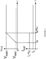
- FIGURE 5 illustrated are timing diagrams demonstrating an operation of a power converter.
- the illustrated embodiment demonstrates an output voltage V out and output current lout of the power converter as a function of time t at start-up.
- the output voltage V out , the output current lout and rise times t r1 , t r2 as set forth herein are employed to compute a capacitance of an output capacitor Cout of the power converter (see, e.g., equation (9)).
- the output voltage V out is ramped up from an initial output voltage V start to a steady-state nominal output voltage of V nom .
- the power train starts with a minimum duty cycle D min and the output voltage V out makes a quick jump to the initial output voltage V start at a time t d , which may include a configurable delay after a remote control signal starts the ramp-up sequence.
- the initial output voltage V start equals n•D min •V in , wherein "n" is a transformer turns ratio for power converters that include an isolation transformer. Otherwise, the transformer turns ratio n is set to one.
- This jump in duty cycle causes a current spike at an output of the power converter to charge the output capacitor C out .
- the output voltage V out ramps up linearly with a slope S1 until a time t d + t r1 .
- the output current I out begins at zero and then transitions to a sum of the load current IL and the capacitor current I C of the output capacitor C out at the time t d .
- the output current I out maintains the sum of the load current I L and the capacitor current I C (designated a first output current I out1 ) until the time t d + t r1 .
- the first output current I out1 exceeds the maximum output current I max .
- the output voltage V out linearly ramps up with a reduced slope S 2 to the steady-state nominal output voltage V nom at a time t d + t r1 +t r2 .
- the sum of the load current I L and the capacitor current I C of the output capacitor C out drops to the maximum output current I max .
- the output current I out levels off at the load current IL.
- the rise time t r2 and slope S 2 of the output voltage V out is adjusted so that the first output current I out1 is reduced to the maximum output current I max .
- I out C out V nom t r 1 + I L , where IL is a steady dc current drawn by the load and V nom is the steady-state output voltage level that is generally regulated to a particular level.
- t r2 C out V nom I max ⁇ I L .
- the output current lout of the power converter will be larger than the maximum output current I max .
- a final adjustment to a rise time t r3 can be made since in this case the load current IL can be calculated and adjusted with two first measurements.
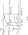
- FIGURE 6 illustrated are timing diagrams demonstrating an operation of a power converter.
- the illustrated embodiment demonstrates an output voltage V out and output current I out of the power converter as a function of time t at start-up.
- the output voltage V out , the output current I out and rise times t r1 , t r2 , t r3 as set forth herein are employed to compute a capacitance of an output capacitor C out of the power converter (see, e.g., equations (9), (10)).
- the output voltage V out is ramped up from an initial output voltage V start to a steady-state nominal output voltage of V nom .
- the power train starts with a minimum duty cycle D min and the output voltage V out makes a quick jump to the initial output voltage V start at a time t d , which may include a configurable delay after a remote control signal starts the ramp-up sequence.
- the initial output voltage V start equals n•D min •V in , wherein "n" is a transformer turns ratio for power converters that include an isolation transformer. Otherwise, the transformer turns ratio n is set to one.
- This jump in duty cycle causes a current spike at an output of the power converter to charge the output capacitor C out .
- the output voltage V out ramps up linearly with a slope S1 until a time t d + t r1 .
- the output current I out begins at zero and then transitions to a sum of the load current I L and the capacitor current I C of the output capacitor C out at the time t d .
- the output current I out maintains the sum of the load current I L and the capacitor current I C (designated a first output current I out1 ) until the time t d + t r1 .
- the first output current I out1 exceeds the maximum output current I max .
- the output voltage V out linearly ramps up with a reduced slope S 2 until a time t d + t r1 + t r2 .
- the output current I out maintains the sum of the load current I L and the capacitor current I C (designated a second output current I out2 ) until the time t d + t r1 + t r2 .
- the second output current I out2 also exceeds the maximum output current I max .
- the output voltage V out linearly ramps up with a reduced slope S 3 to the steady-state nominal output voltage V nom at a time t d + t r1 + t r2 + t r3 .
- the sum of the load current IL and the capacitor current I C of the output capacitor Cout drops to the maximum output current I max .
- the output current I out levels off at the load current IL.
- the rise time t r3 and slope S 3 of the output voltage V out are adjusted so that the first and second output currents I out1 , I out2 are reduced to the maximum output current I max .
- a power converter including an output capacitor (C out ) couplable in parallel to a dissipative load (LD) (drawing a load current (I L )) has been introduced herein.
- the power converter includes a power train (240) configured to convert an input voltage (V in ) to a nominal output voltage (Vnom) and a controller (210) including a processor (220) and memory (230).
- the controller (210) is configured to ramp up an output voltage (V out ) of the power converter with a first slope (S 1 ) ( e.g., a default slope) and a second slope (S 2 ) ( e.g., being reduced with respect to the first slope (S 1 )), and receive a first output current (I out1 ) of the power converter during a first rise time (tr 1 ) associated with the first slope (S 1 ) and a second output current (I out2 ) of the power converter during a second rise time (t r2 ) associated with the second slope (S 2 ).
- a first slope (S 1 ) e.g., a default slope
- S 2 e.g., being reduced with respect to the first slope (S 1 )
- the controller (210) is also configured to compute a capacitance of the output capacitor (C out ) employing the first and second output currents (I out1 , I out2 ), the first and second rise times (t r1 , t r2 ) (and/or the first and second slopes (S 1 , S 2 )), and the nominal output voltage (V nom ).
- the controller (210) is further configured to compute a current (I C ) supplied to the output capacitor (C out ) employing the first output current (I out1 ) of the power converter during the first rise time (t r1 ) and the second output current (I out2 ) of the power converter during the second rise time (tr 2 ).
- the controller (210) is also configured to receive the first output current (I out1 ) and select the second rise time (t r2 ) so that the second output current (I out2 ) does not exceed a maximum output current (I max ) of the power converter.
- the controller (210) is also configured to shut down the power converter if the output voltage (V out ) cannot reach a minimum output voltage threshold (V min ).
- the controller (210) is also configured to select a third slope (S 3 ) associated with a third rise time (t r3 ) if the second output current (I out2 ) is greater than a maximum output current (I max ) or exceeds an over-current protection level (I OCP ).
- FIGURE 7 illustrated is a flow diagram of an embodiment of a method of operating a power converter.
- the method is operable to measure parameters such as an output voltage V out , an output current I out and rise times t r to compute a capacitance of an output capacitor of a power converter and begins at a start step or module 705.
- the output voltage V out of the power converter is ramped up having an initial default slope with a default rise time t r at a step or module 710. Thereafter, the output current lout of the power converter is measured at a step or module 715.
- the output current lout is compared against a maximum output current I max or an over-current protection limit I OCP of the power converter. If the output current I out is less than the maximum output current I max and the over-current protection limit I OCP , the output voltage V out continues to be ramped up with the initial slope, at a step or module 725, until the output voltage V out reaches a nominal output voltage V nom and normal operation is attained at a step or module 760.
- step or module 730 If the output current lout is greater than the maximum output current I max , a new slope and rise time tr are determined, in a step or module 730, and the output voltage V out of the power converter is ramped up having the new slope with the new rise time tr at a step or module 735. If the output current lout continues to be greater than the maximum output current I max (as demonstrated by the dotted path), the step or modules 730, 735 are repeated until the output current lout is less than the maximum output current I max and then the power converter transitions to normal operation as depicted in the step or module 760.
- the output current I out is greater than the over-current protection limit I OCP , the output voltage V out of the power converter is ramped up having a new slope with a new rise time tr and a constant current in a step or module 740. Thereafter, the rise time tr is measured in a step or module 745 and the output voltage V out is measured in a step or module 750. If the rise time tr is greater than a maximum rise time or the output voltage V out is less than a minimum output voltage threshold, then the power converter is shut down in a step or module 755.
- the power converter may stop until a reset signal is obtained, which is also known as "latched protection," or, in another configuration, a retry is attempted within a certain time, also known as a “hick-up.”
- a reset signal is obtained, which is also known as "latched protection”
- a retry is attempted within a certain time, also known as a "hick-up.”
- the output voltage V out is also monitored and if the output voltage V out remains lower than the minimum output voltage threshold, the power converter shuts down according to the configuration. If neither one of the conditions are met, then the power converter transitions to normal operation as depicted in the step or module 760.
- Measuring output current lout of the power converter employing the process illustrated in FIGURE 7 using a plurality of slopes for the output voltage V out in at least two time intervals enables computation of the capacitance coupled across the output of the power converter.
- the look-up of a new rise time tr can be performed several times, if, for instance, the output current lout changes during the ramp-up interval. If the output current I out increases too much above the over-current protection level I OCP , a constant current ramp-up state can be entered.
- FIGURE 8 illustrated is a flow diagram of an embodiment of a method of operating a power converter.
- the power converter is configured to convert an input voltage to a nominal output voltage.
- the power converter includes a power train with an output capacitor couplable in parallel to a dissipative load (drawing a load current).
- the method begins at a start step or module 805.
- the method includes ramping up the output voltage of the power converter with an initial slope (e.g., a default slope), then receiving and measuring an output current of the power converter during an initial rise time associated with the initial slope at a step or module 815.
- an initial slope e.g., a default slope
- the method includes determining if the output current of the power converter exceeds a threshold such as a maximum output current and/or an over-current protection limit. If the output current exceeds the threshold, the method includes selecting another slope (e.g., being reduced with respect to the initial slope) at a step or module 825 and then ramping up the output voltage with the another slope at a step or module 830. At a step or module 835, the method includes receiving and measuring the output current of the power converter during another rise time associated with the another slope.
- a threshold such as a maximum output current and/or an over-current protection limit.
- the method includes determining if the another rise time is greater than a maximum rise time at a decisional step or module 840. If the another rise time is greater than a maximum rise time, then the method includes shutting down the power converter at a step or module 845 and then the method ends at a step or module 850. If the another rise time is not greater than a maximum rise time, then the method determines if the output voltage is less than a minimum output voltage threshold at a decisional step or module 855. If the output voltage is less than a minimum output voltage threshold, then the method includes shutting down the power converter at the step or module 845 and then the method ends at the step or module 850. If the output voltage is not less than a minimum output voltage threshold, then the method returns to the decisional step or module 820.
- the method includes ramping up the output voltage at the present slope until the output voltage reaches the nominal output voltage at a step or module 860.
- the method then includes computing a current of an output capacitor of the power converter at a step or module 865.
- the method includes computing a capacitance of the output capacitor and the method concludes at the step or module 850.
- the capacitance of the output capacitor is a function of the output current(s), the slopes and the rise time(s), and the nominal output voltage.
- the exemplary embodiment provides both a method and corresponding apparatus consisting of various modules providing functionality for performing the steps of the method.
- the modules may be implemented as hardware (embodied in one or more chips including an integrated circuit such as an application specific integrated circuit), or may be implemented as software or firmware for execution by a processor.
- firmware or software the exemplary embodiment can be provided as a computer program product including a computer readable storage medium embodying computer program code (i.e., software or firmware) thereon for execution by the computer processor.
- the computer readable storage medium may be non-transitory (e.g ., magnetic disks; optical disks; read only memory; flash memory devices; phase-change memory) or transitory (e.g ., electrical, optical, acoustical or other forms of propagated signals-such as carrier waves, infrared signals, digital signals, etc. ).
- the coupling of a processor and other components is typically through one or more busses or bridges (also termed bus controllers).
- the storage device and signals carrying digital traffic respectively represent one or more non-transitory or transitory computer readable storage medium.
- the storage device of a given electronic device typically stores code and/or data for execution on the set of one or more processors of that electronic device such as a controller.
Landscapes
- Engineering & Computer Science (AREA)
- Power Engineering (AREA)
- Physics & Mathematics (AREA)
- General Physics & Mathematics (AREA)
- Dc-Dc Converters (AREA)
Description
- The present invention is directed, in general, to the field of power electronics and, more specifically, to a system and method to determine a capacitance of a capacitor.
- A switched-mode power converter is a type of power converter having a diverse range of applications by virtue of its small size, weight and high efficiency. For example, switched-mode power converters are widely used in personal computers and portable electronic devices such as cellphones. A switching device (e.g., a metal-oxide semiconductor field-effect transistor ("MOSFET")) of a power train of t e switched mode power converter is controlled to convert an input voltage to a desired output voltage. A frequency and duty cycle of t e switching device is adjusted using a feedback signal to convert the input voltage to the desired output voltage.
- A feedback loop of the power converter that provides the feedback signal may be monitored and adjusted to enhance the regulation of the output characteristic such as the output voltage. Dynamic elements of the power converter such as inductors and capacitors can affect the feedback loop design parameters. A capacitance of an output capacitor is not only dependent on internal capacitances of the power converter, but also load capacitances that can vary from application to application.
- The feedback loop performance affects input and output currents produced by the power converter during startup-up as well as the ability to regulate the output characteristic in the presence of load transients. The inductors are generally included internally in the power converter design and, thus, provide known reactive values for the design of the feedback loop. The design of the feedback loop, however, is dependent on load capacitances that are unknown or only partially known during the design phase. Technical developments over time have improved electrical characteristics of capacitors such that they can have a higher capacitance in a given physical size as well as a lower equivalent series resistance ("ESR"). That being said, the unknown load capacitances still can have a significant effect on feedback loop performance. Related art within this technical field is disclosed, for e.g. D1:
EP2704300A1, filed August 6, 2012 , entitled "Method for controlling a power stage", describes a background art of method for controlling a DC-DC power converter. - The invention is defined by the independent claims. Furthermore, embodiments of the invention are defined by the claims. These and other problems are generally solved or circumvented, and technical advantages are generally achieved, by advantageous embodiments of the present invention for a system and method to determine a capacitance of a capacitor. In one embodiment, a power converter includes a controller coupled to an output capacitor and a power train configured to convert an input voltage to a nominal output voltage. The controller is configured to ramp up an output voltage of the power converter with a first slope and a second slope, and receive a first output current of the power converter during a first rise time associated with the first slope and a second output current of the power converter during a second rise time associated with the second slope. The controller is also configured to compute a capacitance of the output capacitor employing the first and second output currents, the first and second rise times, and the nominal output voltage. Corresponding embodiments are also applicable for a method of operating a power converter and a controller for use with a power converter.
- The foregoing has outlined rather broadly the features and technical advantages of the present invention in order that the detailed description of the invention that follows may be better understood. Additional features and advantages of the invention will be described hereinafter, which form the subject of the claims of the invention. It should be appreciated by those skilled in the art that the conception and specific embodiment disclosed may be readily utilized as a basis for modifying or designing other structures or processes for carrying out the same purposes of the present invention.
- For a more complete understanding of the present invention, reference is now made to the following descriptions taken in conjunction with the accompanying drawings, in which:
-
FIGURE 1 illustrates a schematic diagram of an embodiment of a power converter; -
FIGURE 2 illustrates a schematic diagram of another embodiment of a power converter; -
FIGURE 3 illustrates timing diagrams demonstrating an operation of the power converter ofFIGURE 2 ; -
FIGUREs 4 to 6 illustrate timing diagrams demonstrating operations of a power converter; and -
FIGUREs 7 and8 illustrate flow diagrams of embodiments of methods of operating a power converter. - Corresponding numerals and symbols in the different figures generally refer to corresponding parts unless otherwise indicated, and may not be redescribed in the interest of brevity after the first instance. The FIGUREs are drawn to illustrate the relevant aspects of exemplary embodiments.
- The making and using of the present exemplary embodiments are discussed in detail below. It should be appreciated, however, that the embodiments provide many applicable inventive concepts that can be embodied in a wide variety of specific contexts. The specific embodiments discussed are merely illustrative of specific ways to make and use the systems, subsystems, and modules associated with determining a capacitance of a capacitor of a power converter. In view of the need to enhance a feedback loop to manage input and output characteristics of a power converter, a system and method to determine parameters of the feedback loop would be beneficial. Of consequence to that determination, a system and method to determine a capacitance of an output capacitor, especially in view of load capacitances would improve the design of the feedback loop.
- A process will be described herein with respect to exemplary embodiments in a specific context, namely, a system and method operable to identify a capacitance of an output capacitor of a power converter. While the principles will be described in the environment of a power converter, a motor controller, or power amplifier that may benefit from such a system and method that enables these functionalities is well within the broad scope of the present disclosure.
- In order to enhance the performance of a feedback loop in a power converter, system dynamic components such as an output capacitance should be properly identified. A common method in system identification is to superimpose a disturbance on an internal signal and analyze what happens on the output, for example, as described in "System Identification - Theory for the User" by L. Ljung (Prentice-Hall, Englewood Cliffs, ISBN 0-13-B81640, 1987). Such a disturbance can be injected in many different ways. One way is to use relay feedback, as described in "Automatic tuning of PID controllers" by K. J. Åström and T. Hägglund (Instrument Society of America, ISBN 1-55617-081-5, 1988). Alternatively, the disturbance can be injected by inducing limit cycles or injecting a noise signal, as described in the doctoral thesis of Zhao Zhenyu, entitled "Design and Practical Implementation of Digital Auto-tuning and Fast-response Controllers for Low-power Switch-mode Power Supplies" (University of Toronto, Canada, 2008).
- A problem with the above schemes is to control or limit an amplitude of the disturbance at the output of the power converter. The loads of the power converter sometimes have very strict requirements on overvoltage, which make such methods difficult to use. Furthermore, in some applications, particularly those in the telecommunications industry, no disturbance at all on the output voltage can be tolerated. The aforementioned methods employing feedback control employ complex calculations that take time and consume power. In addition, these solutions place heavy demands on computational resources. Other methods that involve injecting sinusoidal disturbances and using cross-correlation to determine the system's transfer function are also time consuming and use complex calculations that take time and consume power, and employ a fair amount of computation resources.
- In addition, the development of new complementary metal-oxide semiconductor ("CMOS") technologies such as application specific integrated circuits ("ASICs") and field programmable gate arrays ("FPGAs") has led to tougher requirements on the current capabilities and voltage tolerance bands of the power converters. Moreover, a bank of capacitors with a mix of different capacitor types is now often used for enhancing the electrical performance of a circuit powered by the power converter. In addition, technical developments have improved the electrical characteristics of the capacitors such that they have a higher capacitance and a lower equivalent series resistance ("ESR"). Thus, the capacitive load can vary widely between different applications.
- It is, therefore, highly desirable to develop a scheme to improve the feedback loop parameters in a power converter that avoids the injection of any disturbance that can cause additional noise on the output voltage of the power converter. This should include a measure of the load capacitance coupled to an output thereof. The load capacitance affects the system dynamics of the power converter and should be considered during the design of the control loop of the power converter.
- Referring initially to
FIGURE 1 , illustrated is a schematic diagram of an embodiment of a power converter. The power converter receives an input voltage Iin and converts a direct current ("dc") input voltage Vin (from an input power source) to a desired dc output voltage Vout. The output voltage Vout is applied across a load (designated "LD") connected in parallel with an output capacitor Cout. An output current lout is split between the output capacitor Cout (receiving a capacitor current Ic) and the load LD (receiving a load current IL). The power converter includes an inductor L, the output capacitor Cout, a diode D1 and apower switch 110. The power converter also includes a controller 130 (including a processor ("PR") 140 and memory ("M") 150) that controls thepower switch 110 to regulate the output voltage Vout of the power converter. - The
controller 130 applies a control signal Cs at an appropriate frequency (e.g., 300 kilohertz ("kHz")) to a control terminal of the power switch (also referred to as a "switching device") 110. Thecontroller 130 regulates the output voltage Vout by adjusting the duty cycle D of the control signal Cs (defined by D=TON/Tswitch, where TON is the duration of the control signal and Tswitch is the conduction interval of the power switch 110) as a function of the output current lout and/or the output voltage Vout. As discussed in more detail below, thecontroller 130 is also configured to compute a capacitance of the output capacitor Cout of the power converter. - Although a single output capacitor Cout is shown in the simplified diagram of
FIGURE 1 , the power converter may use large banks of capacitors for maintaining a stable output voltage Vout during load transients or for keeping the voltage ripple at an acceptable level. The power converter illustrated inFIGURE 1 is not limited to the above-described buck topology, and the apparatus and methods introduced herein will work equally well with many topologies including push-pull, half-bridge and forward converters, etc. Further, it will be appreciated that the techniques of the solution introduced herein are applicable to various types of switched mode power supplies (e.g., dc-dc, etc). - The
processor 140 may be embodied as any type of processor and associated circuitry configured to perform one or more of the functions described herein. For example, theprocessor 140 may be embodied as or otherwise include a single or multicore processor, an application specific integrated circuit, a collection of logic devices, or other circuits. Thememory 150 may be embodied as read-only memory devices and/or random access memory devices. For example, thememory 150 may be embodied as or otherwise include dynamic random access memory devices ("DRAM"), synchronous dynamic random access memory devices ("SDRAM"), double-data rate dynamic random access memory devices ("DDR SDRAM"), and/or other volatile or non-volatile memory devices. Thememory 150 may have stored therein programs including a plurality of instructions or computer program code for execution by theprocessor 140 to control particular functions of the power converter as discussed in more detail below. - Turning now to
FIGURE 2 , illustrated is a schematic diagram of another embodiment of a power converter. A power train of the power converter receives an input voltage Iin and an input voltage Vin and includes first and second high-side switching devices Q1, Q2, and first and second low-side switching devices Q3, Q4 arranged in a full bridge configuration and including parasitic capacitances (illustrated with dotted lines as parallel capacitances). The first high-side switching device Q1 is coupled in series at a first circuit node Va with the first low-side switching device Q3. The second high-side switching device Q2 is coupled in series at a second circuit node Vb with the second low-side switching device Q4. The first and second circuit nodes Va, Vb are coupled to opposite ends of a primary winding of a transformer TR. A secondary winding of the transformer TR is coupled to a synchronous rectifier formed by a third low-side switching device Q5 (including a parasitic capacitance, not shown) coupled to a fourth low-side switching device Q6 (including a parasitic capacitance, not shown). A center tap of the secondary winding of the transformer TR is coupled to an output filter including output inductor L and output capacitor Cout that filters an output voltage Vout provided to a load (designated "LD"). An output current lout is split between the output capacitor Cout (receiving a capacitor current Ic) and the load LD (receiving a load current IL). - The first and second high-side switching devices Q1, Q2, and the first and second low-side switching devices Q3, Q4 are controlled to provide a high frequency ac voltage to the primary winding of the transformer TR. The high frequency ac voltage is impressed across to the secondary winding of the transformer TR and the third and fourth low-side switching devices Q5, Q6 are controlled to provide a rectified dc voltage. The rectified dc voltage is then filtered by the output filter, which provides the output voltage Vout to the load LD. While the switching devices are illustrated as MOSFETs, it should be understood that any semiconductor switch technology can be used as the application dictates. Also, while the power train includes a full bridge configuration and synchronous rectifier, other topologies and rectification techniques may be employed to advantage.
- A
controller 210 including a processor ("PR") 220 and memory ("M") 230 receives the output current lout and/or the output voltage Vout and generates control signals Cs1, Cs2, Cs3, Cs4 for the first and second high-side switching devices Q1, Q2, and first and second low-side switching devices Q3, Q4 to regulate the output voltage Vout (an output characteristic of the power converter). Thecontroller 210 also generates control signals Cs5, Cs6 for the synchronous rectifier formed by the third and fourth low-side switching devices Q5, Q6. A description ofanalogous controller 130 is described above with respect toFIGURE 1 . As discussed in more detail below, thecontroller 210 is also configured to compute a capacitance of the output capacitor Cout of the power converter. - Turning now to
FIGURE 3 , illustrated are timing diagrams demonstrating an operation of the power converter ofFIGURE 2 . The timing diagrams represent the conduction intervals for the switching devices Q1, Q2, Q3, Q4, Q5, Q6 over a switching interval T as a function of time t (on the horizontal axis). The first high-side switching device Q1 and the second low-side switching device Q4 conduct for a duty cycle D delivering energy to the transformer TR. The fourth low-side switching device Q6 is also conducting during this time. During a freewheeling phase (from the duty cycle D to half the switching interval T/2), the first and second high-side switching devices Q1, Q2, and the first and second low-side switching devices Q3, Q4 are non-conducting, and a current in the output inductor L flows through the third and fourth low-side switching devices Q5, Q6 of the synchronous rectifier. - For a period representing a duty cycle D (from half the switching interval T/2 to half the switching interval plus the duty cycle T/2+D), the second high-side switching device Q2 and the first low-side switching device Q3 conduct delivering energy to the transformer TR. The third low-side switching device Q5 is also conducting during this time. During another freewheeling phase (from half the switching interval plus the duty cycle T/2+D to the end of the switching interval T), the first and second high-side switching devices Q1, Q2, and the first and second low-side switching devices Q3, Q4 are non-conducting, and a current in the output inductor L flows through the third and fourth low-side switching devices Q5, Q6 of the synchronous rectifier.
- Turning now to
FIGURE 4 , illustrated are timing diagrams demonstrating an operation of a power converter. The illustrated embodiment demonstrates an output voltage Vout and output current Iout of the power converter as a function of time t at start-up. The output voltage Vout, the output current lout and a rise time tr1 a set forth below are employed to compute a capacitance of an output capacitor Cout of the power converter (see, e.g., equation (9)). Through operation of the power train (e.g., the switching devices ofFIGURE 2 ), the output voltage Vout is ramped up from an initial output voltage Vstart to a steady-state nominal output voltage (also referred to as a "nominal output voltage") Vnom. The power train starts with a minimum duty cycle Dmin and the output voltage Vout makes a quick jump to the initial output voltage Vstart at a time td, which may include a configurable delay after a remote control signal starts the ramp-up sequence. The initial output voltage Vstart equals n•Dmin•Vin, wherein "n" is a transformer turns ratio for power converters that include an isolation transformer. Otherwise, the transformer turns ratio n is set to one. This jump in duty cycle causes a current spike at an output of the power converter to charge the output capacitor Cout. Through the operation of the power train, the output voltage Vout ramps up linearly to the steady-state nominal output voltage Vnom at a time td + tr1. - The output current lout begins at zero and then transitions to a sum of the load current IL and the capacitor current Ic of the output capacitor Cout at the time td. The capacitor current Ic of the output capacitor Cout can be calculated as:

- In systems where, for example, the output capacitor Cout is formed with a capacitor bank and the capacitance is very large, the capacitor current Ic may be larger than the output current lout capability of the power converter. In other instances, the input current Iin consumed by the power converter may cause problems with the power source to the power converter. The instantaneous current charging for the output capacitor Cout generally cannot be distinguished by the power converter from the dissipative load current IL drawn by the load.
- As introduced herein, the output current lout is measured and includes current flowing in substantially all capacitances (designated as the output capacitor Cout) coupled across the output of the power converter. If the load current IL and capacitor current IC are larger than a maximum output current Imax of the power converter, the rise time tr1 is adjusted so that the output current lout is equal to or less than the maximum output current Imax.
- The process introduced herein enables computation of the value of total capacitance represented by the output capacitor Cout coupled across the output terminals of a power converter as well as a dissipative load current IL coupled thereto. Knowing a value of total capacitance coupled across output terminals of the power converter can enable an auto-tuning procedure or algorithm in a feedback loop that makes it possible to accommodate in the feedback loop, for example, aging components and component value temperature drift in a real application.
- Turning now to
FIGURE 5 , illustrated are timing diagrams demonstrating an operation of a power converter. The illustrated embodiment demonstrates an output voltage Vout and output current lout of the power converter as a function of time t at start-up. The output voltage Vout, the output current lout and rise times tr1, tr2 as set forth herein are employed to compute a capacitance of an output capacitor Cout of the power converter (see, e.g., equation (9)). Through operation of the power train (e.g., the switching devices ofFIGURE 2 ), the output voltage Vout is ramped up from an initial output voltage Vstart to a steady-state nominal output voltage of Vnom. The power train starts with a minimum duty cycle Dmin and the output voltage Vout makes a quick jump to the initial output voltage Vstart at a time td, which may include a configurable delay after a remote control signal starts the ramp-up sequence. As mentioned above, the initial output voltage Vstart equals n•Dmin•Vin, wherein "n" is a transformer turns ratio for power converters that include an isolation transformer. Otherwise, the transformer turns ratio n is set to one. This jump in duty cycle causes a current spike at an output of the power converter to charge the output capacitor Cout. Through the operation of the power train, the output voltage Vout ramps up linearly with a slope S1 until a time td + tr1. - Regarding the output current Iout, the output current Iout begins at zero and then transitions to a sum of the load current IL and the capacitor current IC of the output capacitor Cout at the time td. The output current Iout maintains the sum of the load current IL and the capacitor current IC (designated a first output current Iout1) until the time td + tr1. The first output current Iout1, however, exceeds the maximum output current Imax.
- Through the operation of the power train, the output voltage Vout linearly ramps up with a reduced slope S2 to the steady-state nominal output voltage Vnom at a time td + tr1+tr2. As a result, the sum of the load current IL and the capacitor current IC of the output capacitor Cout drops to the maximum output current Imax. After reaching the steady-state nominal output voltage Vnom, the output current Iout levels off at the load current IL. Thus, the rise time tr2 and slope S2 of the output voltage Vout is adjusted so that the first output current Iout1 is reduced to the maximum output current Imax.
- With continuing reference to
FIGUREs 4 and5 , the output current lout during the rise time tr1 is given by the equation (1) below:
- If it is assumed that the maximum allowed current during the ramp-up is Imax, equation (2) below can be obtained to indicate the maximum output current Imax dependent on a rise time tr2:

- The new rise time tr2 can be solved using equation (2) above to produce equation (3) below:


- Assuming the steady dc load current IL is zero in the beginning before a power-on reset of the load is performed, equation (4) can be simplified to:

- In a common situation where the load current IL is non-zero during start-up, equation (6) below can be used to calculate the new rise time tr2:

- In a normal case, a safety margin is used limiting the allowed maximum load current, for example, max[IL] = Imax/4. This yields in equation (7) the following maximum rise time for the new rise time tr2:

- If the load current IL is larger than the assumed safety margin, the output current lout of the power converter will be larger than the maximum output current Imax. In this case, a final adjustment to a rise time tr3 can be made since in this case the load current IL can be calculated and adjusted with two first measurements.
- Assuming that the initial rise time tr1 is much less than the subsequent rise time tr2 (the output voltage Vout after the first two measurement times is much lower than the steady-state nominal output voltage Vnom) two equations are obtained with two unknowns, the output capacitor Cout and the load current IL, which can be solved using equation (8) below:


- Hence, using two measurements with two different rise times (and the corresponding slopes), the values of the output capacitor Cout and the load current IL can be identified, which extends the results introduced by
Karlsson et al., in U.S. Patent No. 8,854,026 , entitled "Capacitance Determination in a Switched Mode Power Supply," issued October 7, 2014, which is incorporated herein by reference. - The final rise time tr3 that yields a maximum output current Imax can also be solved for using equation (10) below:

- Turning now to
FIGURE 6 , illustrated are timing diagrams demonstrating an operation of a power converter. The illustrated embodiment demonstrates an output voltage Vout and output current Iout of the power converter as a function of time t at start-up. The output voltage Vout, the output current Iout and rise times tr1, tr2, tr3 as set forth herein are employed to compute a capacitance of an output capacitor Cout of the power converter (see, e.g., equations (9), (10)). Through operation of the power train (e.g., the switching devices ofFIGURE 2 ), the output voltage Vout is ramped up from an initial output voltage Vstart to a steady-state nominal output voltage of Vnom. The power train starts with a minimum duty cycle Dmin and the output voltage Vout makes a quick jump to the initial output voltage Vstart at a time td, which may include a configurable delay after a remote control signal starts the ramp-up sequence. As mentioned above, the initial output voltage Vstart equals n•Dmin•Vin, wherein "n" is a transformer turns ratio for power converters that include an isolation transformer. Otherwise, the transformer turns ratio n is set to one. This jump in duty cycle causes a current spike at an output of the power converter to charge the output capacitor Cout. Through the operation of the power train, the output voltage Vout ramps up linearly with a slope S1 until a time td + tr1. - Regarding the output current Iout, the output current Iout begins at zero and then transitions to a sum of the load current IL and the capacitor current IC of the output capacitor Cout at the time td. The output current Iout maintains the sum of the load current IL and the capacitor current IC (designated a first output current Iout1) until the time td + tr1. The first output current Iout1, however, exceeds the maximum output current Imax.
- Through the operation of the power train, the output voltage Vout linearly ramps up with a reduced slope S2 until a time td + tr1 + tr2. The output current Iout maintains the sum of the load current IL and the capacitor current IC (designated a second output current Iout2) until the time td + tr1 + tr2. The second output current Iout2, however, also exceeds the maximum output current Imax.
- Through the operation of the power train, the output voltage Vout linearly ramps up with a reduced slope S3 to the steady-state nominal output voltage Vnom at a time td + tr1 + tr2 + tr3. As a result, the sum of the load current IL and the capacitor current IC of the output capacitor Cout drops to the maximum output current Imax. After reaching the steady-state nominal output voltage Vnom, the output current Iout levels off at the load current IL. Thus, the rise time tr3 and slope S3 of the output voltage Vout are adjusted so that the first and second output currents Iout1, Iout2 are reduced to the maximum output current Imax.
- A power converter including an output capacitor (Cout) couplable in parallel to a dissipative load (LD) (drawing a load current (IL)) has been introduced herein. The power converter includes a power train (240) configured to convert an input voltage (Vin) to a nominal output voltage (Vnom) and a controller (210) including a processor (220) and memory (230). The controller (210) is configured to ramp up an output voltage (Vout) of the power converter with a first slope (S1) (e.g., a default slope) and a second slope (S2) (e.g., being reduced with respect to the first slope (S1)), and receive a first output current (Iout1) of the power converter during a first rise time (tr1) associated with the first slope (S1) and a second output current (Iout2) of the power converter during a second rise time (tr2) associated with the second slope (S2). The controller (210) is also configured to compute a capacitance of the output capacitor (Cout) employing the first and second output currents (Iout1, Iout2), the first and second rise times (tr1, tr2) (and/or the first and second slopes (S1, S2)), and the nominal output voltage (Vnom).
- The controller (210) is further configured to compute a current (IC) supplied to the output capacitor (Cout) employing the first output current (Iout1) of the power converter during the first rise time (tr1) and the second output current (Iout2) of the power converter during the second rise time (tr2). The controller (210) is also configured to receive the first output current (Iout1) and select the second rise time (tr2) so that the second output current (Iout2) does not exceed a maximum output current (Imax) of the power converter. The controller (210) is also configured to shut down the power converter if the output voltage (Vout) cannot reach a minimum output voltage threshold (Vmin). The controller (210) is also configured to select a third slope (S3) associated with a third rise time (tr3) if the second output current (Iout2) is greater than a maximum output current (Imax) or exceeds an over-current protection level (IOCP).
- Turning now to
FIGURE 7 , illustrated is a flow diagram of an embodiment of a method of operating a power converter. The method is operable to measure parameters such as an output voltage Vout, an output current Iout and rise times tr to compute a capacitance of an output capacitor of a power converter and begins at a start step ormodule 705. Through operation of a power train of the power converter, the output voltage Vout of the power converter is ramped up having an initial default slope with a default rise time tr at a step ormodule 710. Thereafter, the output current lout of the power converter is measured at a step ormodule 715. At a step ormodule 720, the output current lout is compared against a maximum output current Imax or an over-current protection limit IOCP of the power converter. If the output current Iout is less than the maximum output current Imax and the over-current protection limit IOCP, the output voltage Vout continues to be ramped up with the initial slope, at a step ormodule 725, until the output voltage Vout reaches a nominal output voltage Vnom and normal operation is attained at a step ormodule 760. - If the output current lout is greater than the maximum output current Imax, a new slope and rise time tr are determined, in a step or
module 730, and the output voltage Vout of the power converter is ramped up having the new slope with the new rise time tr at a step ormodule 735. If the output current lout continues to be greater than the maximum output current Imax (as demonstrated by the dotted path), the step ormodules module 760. - If the output current Iout is greater than the over-current protection limit IOCP, the output voltage Vout of the power converter is ramped up having a new slope with a new rise time tr and a constant current in a step or
module 740. Thereafter, the rise time tr is measured in a step ormodule 745 and the output voltage Vout is measured in a step ormodule 750. If the rise time tr is greater than a maximum rise time or the output voltage Vout is less than a minimum output voltage threshold, then the power converter is shut down in a step or module 755. For example, the power converter may stop until a reset signal is obtained, which is also known as "latched protection," or, in another configuration, a retry is attempted within a certain time, also known as a "hick-up." Thus, during the constant current ramp-up, the output voltage Vout is also monitored and if the output voltage Vout remains lower than the minimum output voltage threshold, the power converter shuts down according to the configuration. If neither one of the conditions are met, then the power converter transitions to normal operation as depicted in the step ormodule 760. - Measuring output current lout of the power converter employing the process illustrated in
FIGURE 7 using a plurality of slopes for the output voltage Vout in at least two time intervals enables computation of the capacitance coupled across the output of the power converter. As an option, the look-up of a new rise time tr can be performed several times, if, for instance, the output current lout changes during the ramp-up interval. If the output current Iout increases too much above the over-current protection level IOCP, a constant current ramp-up state can be entered. - Turning now to
FIGURE 8 , illustrated is a flow diagram of an embodiment of a method of operating a power converter. The power converter is configured to convert an input voltage to a nominal output voltage. In an embodiment, the power converter includes a power train with an output capacitor couplable in parallel to a dissipative load (drawing a load current). The method begins at a start step ormodule 805. At a step ormodule 810, the method includes ramping up the output voltage of the power converter with an initial slope (e.g., a default slope), then receiving and measuring an output current of the power converter during an initial rise time associated with the initial slope at a step ormodule 815. - At a decisional step or
module 820, the method includes determining if the output current of the power converter exceeds a threshold such as a maximum output current and/or an over-current protection limit. If the output current exceeds the threshold, the method includes selecting another slope (e.g., being reduced with respect to the initial slope) at a step ormodule 825 and then ramping up the output voltage with the another slope at a step ormodule 830. At a step ormodule 835, the method includes receiving and measuring the output current of the power converter during another rise time associated with the another slope. - When the threshold is the over-current protection limit, the method includes determining if the another rise time is greater than a maximum rise time at a decisional step or
module 840. If the another rise time is greater than a maximum rise time, then the method includes shutting down the power converter at a step ormodule 845 and then the method ends at a step ormodule 850. If the another rise time is not greater than a maximum rise time, then the method determines if the output voltage is less than a minimum output voltage threshold at a decisional step ormodule 855. If the output voltage is less than a minimum output voltage threshold, then the method includes shutting down the power converter at the step ormodule 845 and then the method ends at the step ormodule 850. If the output voltage is not less than a minimum output voltage threshold, then the method returns to the decisional step ormodule 820. - Returning to the decisional step or
module 820, if the output current does not exceed the threshold, the method includes ramping up the output voltage at the present slope until the output voltage reaches the nominal output voltage at a step ormodule 860. The method then includes computing a current of an output capacitor of the power converter at a step ormodule 865. At a step ormodule 870, the method includes computing a capacitance of the output capacitor and the method concludes at the step ormodule 850. The capacitance of the output capacitor is a function of the output current(s), the slopes and the rise time(s), and the nominal output voltage. - The foregoing description of embodiments of the present proposed solution has been presented for the purpose of illustration and description. It is not intended to be exhaustive or to limit the proposed solution to the present form disclosed.
- As described above, the exemplary embodiment provides both a method and corresponding apparatus consisting of various modules providing functionality for performing the steps of the method. The modules may be implemented as hardware (embodied in one or more chips including an integrated circuit such as an application specific integrated circuit), or may be implemented as software or firmware for execution by a processor. In particular, in the case of firmware or software, the exemplary embodiment can be provided as a computer program product including a computer readable storage medium embodying computer program code (i.e., software or firmware) thereon for execution by the computer processor. The computer readable storage medium may be non-transitory (e.g., magnetic disks; optical disks; read only memory; flash memory devices; phase-change memory) or transitory (e.g., electrical, optical, acoustical or other forms of propagated signals-such as carrier waves, infrared signals, digital signals, etc.). The coupling of a processor and other components is typically through one or more busses or bridges (also termed bus controllers). The storage device and signals carrying digital traffic respectively represent one or more non-transitory or transitory computer readable storage medium. Thus, the storage device of a given electronic device typically stores code and/or data for execution on the set of one or more processors of that electronic device such as a controller.
- Many of the features and functions discussed above can be implemented in software, hardware, or firmware, or a combination thereof.
Claims (15)
- A controller (210) for use with a power converter coupled to an output capacitor (Cout) including a power train (240) configured to convert an input voltage (Vin) to a nominal output voltage (Vnom), said controller (210), comprising:a processor (220); anda memory (230) including computer program code, wherein said processor (220), said memory (230), and said computer program code are collectively operable to:ramp up an output voltage (Vout) of said power converter with a first slope (51) and a second slope (S2),receive a first output current (Iouti) of said power converter during a first rise time (tri) associated with said first slope (Si) and a second output current (2) of said power converter during a second rise time (te) associated with said second slope compute a capacitance of said output capacitor (Cout) employing said first and second output currents (Iouti, 2), said first and second rise times (tri, tn), and said nominal output voltage (Vnom);characterized in that they are further operable toselect a third slope (S3) associated with a third rise time (to) if said second output current (2) is greater than a maximum output current (Imax).
- The controller (210) as recited in Claim 1 wherein said memory (230) and said computer program code are further configured to, with said processor (220) cause said controller (210) to compute a current (Ic) supplied to said output capacitor (Cout) employing said first output current (Wi) of said power converter during said first rise time (tri) and said second output current (2) of said power converter during said second rise time (tri).
- The controller (210) as recited in Claim 1 wherein said memory (230) and said computer program code are further configured to, with said processor (220) cause said controller (210) to receive said first output current (Iouti) and select said second rise time (to) so that said second output current (Iout2) does not exceed a maximum output current (Imax) of said power converter.
- The controller (210) as recited in Claim 1 wherein said memory (230) and said computer program code are further configured to, with said processor (220) cause said controller (210) to shut down said power converter if said output voltage (Vout) cannot reach a minimum output voltage threshold (Vmin).
- A power converter coupled to an output capacitor (Cout), comprising: a power train (240) configured to convert an input voltage (Vm) to a nominal output voltage (Vnom); and
a controller (210) configured to
ramp up an output voltage (Vout) of said power converter with a first slope (51) and a second slope (S2),
receive a first output current (Iouti) of said power converter during a first rise time (tri) associated with said first slope (Si) and a second output current (2) of said power converter during a second rise time (to) associated with said second slope compute a capacitance of said output capacitor (Com) employing said first and second output currents (Iouti, 2), said first and second rise times (to, to), and said nominal output voltage (Vnom);
characterized by being further configured to
select a third slope (S3) associated with a third rise time (te) if said second output current (2) is greater than a maximum output current (Imax). - The power converter as recited in Claim 5 wherein said controller (210) is further configured to compute a current (Ic) supplied to said output capacitor (Com) employing said first output current (Iouti) of said power converter during said first rise time (to) and said second output current (2) of said power converter during said second rise time (to).
- The power converter as recited in Claim 5 wherein said output capacitor (Com) is couplable in parallel to a dissipative load (LD); and/or wherein said dissipative load (LD) is configured to conduct a load current (II).
- The power converter as recited in Claim 5 wherein said controller (210) is configured to receive said first output current (Iomi) and select said second rise time (to) so that said second output current (2) does not exceed a maximum output current (Imax) of said power converter.
- The power converter as recited in Claim 5 wherein said second slope (S2) is reduced with respect to said first slope (Si); and/or wherein said first slope (Si) is a default slope.
- The power converter as recited in Claim 5 wherein said controller (210) is configured to shut down said power converter if said output voltage (Vom) cannot reach a minimum output voltage threshold (Vmin).
- The power converter as recited in Claim 5 wherein said controller (210) is configured to cause said power converter to select said third slope (S3) if said second output current (2) exceeds an over-current protection level (IOCP).
- A method of operating a power converter coupled to an output capacitor (Cout) including a power train (240) configured to convert an input voltage (Vin) to a nominal output voltage (Vnom), the method, comprising:ramping up an output voltage (Vout) of said power converter with a first slope (Si) and a second slope (S2);receiving a first output current (Iouti) of said power converter during a first rise time (tri) associated with said first slope (Si) and a second output current (2) of said power converter during a second rise time (to) associated with said second slope (S2) ; andcomputing a capacitance of said output capacitor (Cout) employing said first and second output currents (Iouti, 2), said first and second rise times (tri, tn), and said nominal output voltage (Vnom);characterized by further comprising selecting a third slope (S3) associated with a third rise time (ta) if said second output current (2) is greater than a maximum output current (Imax).
- The method as recited in Claim 16 further comprising computing a current (Ic) supplied to said output capacitor (Cout) employing said first output current (Iouti) of said power converter during said first rise time (tri) and said second output current (2) of said power converter during said second rise time (tri).
- The method as recited in Claim 16 further comprising receiving said first output current (Iouti) and selecting said second rise time (ta) so that said second output current (2) does not exceed a maximum output current (Imax) of said power converter.
- The method as recited in Claim 16 further comprising shutting down said power converter if said output voltage (Vout) cannot reach a minimum output voltage threshold (Vmin).
Applications Claiming Priority (1)
| Application Number | Priority Date | Filing Date | Title |
|---|---|---|---|
| PCT/IB2016/054125 WO2018007858A1 (en) | 2016-07-08 | 2016-07-08 | System and method to determine a capacitance of a capacitor |
Publications (2)
| Publication Number | Publication Date |
|---|---|
| EP3482486A1 EP3482486A1 (en) | 2019-05-15 |
| EP3482486B1 true EP3482486B1 (en) | 2020-03-25 |
Family
ID=56409665
Family Applications (1)
| Application Number | Title | Priority Date | Filing Date |
|---|---|---|---|
| EP16738563.2A Active EP3482486B1 (en) | 2016-07-08 | 2016-07-08 | System and method to determine a capacitance of a capacitor |
Country Status (3)
| Country | Link |
|---|---|
| US (1) | US10890608B2 (en) |
| EP (1) | EP3482486B1 (en) |
| WO (1) | WO2018007858A1 (en) |
Families Citing this family (5)
| Publication number | Priority date | Publication date | Assignee | Title |
|---|---|---|---|---|
| US10491125B2 (en) * | 2018-02-12 | 2019-11-26 | Silanna Asia Pte Ltd | Switched-mode power controller with multi-mode startup |
| US10175278B1 (en) * | 2018-04-23 | 2019-01-08 | Linear Technology Holding Llc | Detecting value of output capacitor in switching regulator |
| US11353904B2 (en) * | 2019-04-30 | 2022-06-07 | Texas Instruments Incorporated | Multi-slope startup voltage regulator system |
| CN114785142A (en) * | 2020-12-21 | 2022-07-22 | 成都芯源系统有限公司 | Control circuit of multi-output circuit and feedback circuit thereof |
| CN117452078B (en) * | 2023-12-26 | 2024-04-05 | 锦浪科技股份有限公司 | Capacitance attenuation prediction method of busbar electrolytic capacitor and photovoltaic system |
Family Cites Families (8)
| Publication number | Priority date | Publication date | Assignee | Title |
|---|---|---|---|---|
| US7852053B2 (en) * | 2005-10-31 | 2010-12-14 | Chil Semiconductor Corporation | Power supply and controller circuits |
| US7923974B2 (en) * | 2008-01-04 | 2011-04-12 | Chil Semiconductor Corporation | Modification of switch activation order in a power supply |
| US7990097B2 (en) * | 2008-09-29 | 2011-08-02 | Rockwell Automation Technologies, Inc. | Power conversion system and method for active damping of common mode resonance |
| CN102804577B (en) | 2009-06-25 | 2016-04-13 | 瑞典爱立信有限公司 | Electric capacity in switched-mode power supply is determined |
| TWI424667B (en) * | 2011-11-21 | 2014-01-21 | Anpec Electronics Corp | Soft-stop device and power convertor using the same |
| EP2704300A1 (en) | 2012-08-06 | 2014-03-05 | Zentrum Mikroelektronik Dresden AG | Method for controlling a power stage |
| US9201107B2 (en) | 2013-07-31 | 2015-12-01 | Taiwan Semiconductor Manufacturing Company Ltd. | Cell characterization with Miller capacitance |
| US10404168B2 (en) * | 2017-06-26 | 2019-09-03 | Active-Semi (Bvi), Inc. | Power converter control apparatus and method |
-
2016
- 2016-07-08 US US16/316,130 patent/US10890608B2/en active Active
- 2016-07-08 EP EP16738563.2A patent/EP3482486B1/en active Active
- 2016-07-08 WO PCT/IB2016/054125 patent/WO2018007858A1/en unknown
Non-Patent Citations (1)
| Title |
|---|
| None * |
Also Published As
| Publication number | Publication date |
|---|---|
| US20190317141A1 (en) | 2019-10-17 |
| EP3482486A1 (en) | 2019-05-15 |
| US10890608B2 (en) | 2021-01-12 |
| WO2018007858A1 (en) | 2018-01-11 |
Similar Documents
| Publication | Publication Date | Title |
|---|---|---|
| EP3482486B1 (en) | System and method to determine a capacitance of a capacitor | |
| US10218283B2 (en) | Insulated synchronous rectification DC/DC converter | |
| JP5453508B2 (en) | Isolated flyback converter with efficient light load operation | |
| CN108512428B (en) | Isolated voltage converter and control method thereof | |
| US9190898B2 (en) | Controller for a power converter and method of operating the same | |
| US9647562B2 (en) | Power conversion with switch turn-off delay time compensation | |
| US10014785B2 (en) | Insulation type switching power source apparatus | |
| US9755509B2 (en) | Control circuit for switching power supply | |
| JP2018126058A (en) | Secondary controller for use in synchronous flyback converter, power converter, and method of controlling synchronous flyback converter | |
| JP6135271B2 (en) | Switching power supply | |
| US8947894B2 (en) | Switched mode power supply including a flyback converter with primary side control | |
| US20160261198A1 (en) | Primary side regulated isolation volatge converter | |
| US20140009970A1 (en) | Controller for a Power Converter and Method of Operating the Same | |
| JP6410554B2 (en) | Switching converter and its control circuit, AC / DC converter, power adapter and electronic device | |
| JP2007236058A (en) | Switching power supply | |
| TW201244346A (en) | Controlling a switched mode power supply with maximised power efficiency | |
| US7190152B2 (en) | Closed-loop digital control system for a DC/DC converter | |
| TWI694666B (en) | A converter and method of drive and control thereof | |
| US9698695B1 (en) | Peak power limitation and overpower protection for switched-mode power supplies | |
| EP3261242A1 (en) | Semiconductor device for power supply control | |
| US20140119059A1 (en) | Split current mirror line sensing | |
| CN107834857B (en) | Power supply control device and insulated switching power supply device | |
| US10944323B2 (en) | Power converter for detecting oscillation of output voltage | |
| JP6358815B2 (en) | Control circuit for digital control power supply circuit, control method, digital control power supply circuit using the same, electronic device and base station | |
| JP5213621B2 (en) | Switching regulator control circuit, control method, switching regulator using them, and charging device |
Legal Events
| Date | Code | Title | Description |
|---|---|---|---|
| STAA | Information on the status of an ep patent application or granted ep patent |
Free format text: STATUS: THE INTERNATIONAL PUBLICATION HAS BEEN MADE |
|
| PUAI | Public reference made under article 153(3) epc to a published international application that has entered the european phase |
Free format text: ORIGINAL CODE: 0009012 |
|
| STAA | Information on the status of an ep patent application or granted ep patent |
Free format text: STATUS: REQUEST FOR EXAMINATION WAS MADE |
|
| 17P | Request for examination filed |
Effective date: 20190111 |
|
| AK | Designated contracting states |
Kind code of ref document: A1 Designated state(s): AL AT BE BG CH CY CZ DE DK EE ES FI FR GB GR HR HU IE IS IT LI LT LU LV MC MK MT NL NO PL PT RO RS SE SI SK SM TR |
|
| AX | Request for extension of the european patent |
Extension state: BA ME |
|
| DAV | Request for validation of the european patent (deleted) | ||
| DAX | Request for extension of the european patent (deleted) | ||
| GRAP | Despatch of communication of intention to grant a patent |
Free format text: ORIGINAL CODE: EPIDOSNIGR1 |
|
| STAA | Information on the status of an ep patent application or granted ep patent |
Free format text: STATUS: GRANT OF PATENT IS INTENDED |
|
| GRAS | Grant fee paid |
Free format text: ORIGINAL CODE: EPIDOSNIGR3 |
|
| INTG | Intention to grant announced |
Effective date: 20200120 |
|
| GRAA | (expected) grant |
Free format text: ORIGINAL CODE: 0009210 |
|
| STAA | Information on the status of an ep patent application or granted ep patent |
Free format text: STATUS: THE PATENT HAS BEEN GRANTED |
|
| AK | Designated contracting states |
Kind code of ref document: B1 Designated state(s): AL AT BE BG CH CY CZ DE DK EE ES FI FR GB GR HR HU IE IS IT LI LT LU LV MC MK MT NL NO PL PT RO RS SE SI SK SM TR |
|
| REG | Reference to a national code |
Ref country code: GB Ref legal event code: FG4D |
|
| REG | Reference to a national code |
Ref country code: DE Ref legal event code: R096 Ref document number: 602016032534 Country of ref document: DE |
|
| REG | Reference to a national code |
Ref country code: AT Ref legal event code: REF Ref document number: 1249730 Country of ref document: AT Kind code of ref document: T Effective date: 20200415 Ref country code: IE Ref legal event code: FG4D |
|
| PG25 | Lapsed in a contracting state [announced via postgrant information from national office to epo] |
Ref country code: NO Free format text: LAPSE BECAUSE OF FAILURE TO SUBMIT A TRANSLATION OF THE DESCRIPTION OR TO PAY THE FEE WITHIN THE PRESCRIBED TIME-LIMIT Effective date: 20200625 Ref country code: FI Free format text: LAPSE BECAUSE OF FAILURE TO SUBMIT A TRANSLATION OF THE DESCRIPTION OR TO PAY THE FEE WITHIN THE PRESCRIBED TIME-LIMIT Effective date: 20200325 Ref country code: RS Free format text: LAPSE BECAUSE OF FAILURE TO SUBMIT A TRANSLATION OF THE DESCRIPTION OR TO PAY THE FEE WITHIN THE PRESCRIBED TIME-LIMIT Effective date: 20200325 |
|
| PG25 | Lapsed in a contracting state [announced via postgrant information from national office to epo] |
Ref country code: GR Free format text: LAPSE BECAUSE OF FAILURE TO SUBMIT A TRANSLATION OF THE DESCRIPTION OR TO PAY THE FEE WITHIN THE PRESCRIBED TIME-LIMIT Effective date: 20200626 Ref country code: BG Free format text: LAPSE BECAUSE OF FAILURE TO SUBMIT A TRANSLATION OF THE DESCRIPTION OR TO PAY THE FEE WITHIN THE PRESCRIBED TIME-LIMIT Effective date: 20200625 Ref country code: SE Free format text: LAPSE BECAUSE OF FAILURE TO SUBMIT A TRANSLATION OF THE DESCRIPTION OR TO PAY THE FEE WITHIN THE PRESCRIBED TIME-LIMIT Effective date: 20200325 Ref country code: LV Free format text: LAPSE BECAUSE OF FAILURE TO SUBMIT A TRANSLATION OF THE DESCRIPTION OR TO PAY THE FEE WITHIN THE PRESCRIBED TIME-LIMIT Effective date: 20200325 Ref country code: HR Free format text: LAPSE BECAUSE OF FAILURE TO SUBMIT A TRANSLATION OF THE DESCRIPTION OR TO PAY THE FEE WITHIN THE PRESCRIBED TIME-LIMIT Effective date: 20200325 |
|
| REG | Reference to a national code |
Ref country code: NL Ref legal event code: MP Effective date: 20200325 |
|
| REG | Reference to a national code |
Ref country code: LT Ref legal event code: MG4D |
|
| PG25 | Lapsed in a contracting state [announced via postgrant information from national office to epo] |
Ref country code: NL Free format text: LAPSE BECAUSE OF FAILURE TO SUBMIT A TRANSLATION OF THE DESCRIPTION OR TO PAY THE FEE WITHIN THE PRESCRIBED TIME-LIMIT Effective date: 20200325 |
|
| PG25 | Lapsed in a contracting state [announced via postgrant information from national office to epo] |
Ref country code: PT Free format text: LAPSE BECAUSE OF FAILURE TO SUBMIT A TRANSLATION OF THE DESCRIPTION OR TO PAY THE FEE WITHIN THE PRESCRIBED TIME-LIMIT Effective date: 20200818 Ref country code: LT Free format text: LAPSE BECAUSE OF FAILURE TO SUBMIT A TRANSLATION OF THE DESCRIPTION OR TO PAY THE FEE WITHIN THE PRESCRIBED TIME-LIMIT Effective date: 20200325 Ref country code: SK Free format text: LAPSE BECAUSE OF FAILURE TO SUBMIT A TRANSLATION OF THE DESCRIPTION OR TO PAY THE FEE WITHIN THE PRESCRIBED TIME-LIMIT Effective date: 20200325 Ref country code: RO Free format text: LAPSE BECAUSE OF FAILURE TO SUBMIT A TRANSLATION OF THE DESCRIPTION OR TO PAY THE FEE WITHIN THE PRESCRIBED TIME-LIMIT Effective date: 20200325 Ref country code: IS Free format text: LAPSE BECAUSE OF FAILURE TO SUBMIT A TRANSLATION OF THE DESCRIPTION OR TO PAY THE FEE WITHIN THE PRESCRIBED TIME-LIMIT Effective date: 20200725 Ref country code: CZ Free format text: LAPSE BECAUSE OF FAILURE TO SUBMIT A TRANSLATION OF THE DESCRIPTION OR TO PAY THE FEE WITHIN THE PRESCRIBED TIME-LIMIT Effective date: 20200325 Ref country code: SM Free format text: LAPSE BECAUSE OF FAILURE TO SUBMIT A TRANSLATION OF THE DESCRIPTION OR TO PAY THE FEE WITHIN THE PRESCRIBED TIME-LIMIT Effective date: 20200325 Ref country code: EE Free format text: LAPSE BECAUSE OF FAILURE TO SUBMIT A TRANSLATION OF THE DESCRIPTION OR TO PAY THE FEE WITHIN THE PRESCRIBED TIME-LIMIT Effective date: 20200325 |
|
| REG | Reference to a national code |
Ref country code: AT Ref legal event code: MK05 Ref document number: 1249730 Country of ref document: AT Kind code of ref document: T Effective date: 20200325 |
|
| REG | Reference to a national code |
Ref country code: DE Ref legal event code: R097 Ref document number: 602016032534 Country of ref document: DE |
|
| PG25 | Lapsed in a contracting state [announced via postgrant information from national office to epo] |
Ref country code: IT Free format text: LAPSE BECAUSE OF FAILURE TO SUBMIT A TRANSLATION OF THE DESCRIPTION OR TO PAY THE FEE WITHIN THE PRESCRIBED TIME-LIMIT Effective date: 20200325 Ref country code: AT Free format text: LAPSE BECAUSE OF FAILURE TO SUBMIT A TRANSLATION OF THE DESCRIPTION OR TO PAY THE FEE WITHIN THE PRESCRIBED TIME-LIMIT Effective date: 20200325 Ref country code: ES Free format text: LAPSE BECAUSE OF FAILURE TO SUBMIT A TRANSLATION OF THE DESCRIPTION OR TO PAY THE FEE WITHIN THE PRESCRIBED TIME-LIMIT Effective date: 20200325 Ref country code: DK Free format text: LAPSE BECAUSE OF FAILURE TO SUBMIT A TRANSLATION OF THE DESCRIPTION OR TO PAY THE FEE WITHIN THE PRESCRIBED TIME-LIMIT Effective date: 20200325 |
|
| REG | Reference to a national code |
Ref country code: DE Ref legal event code: R119 Ref document number: 602016032534 Country of ref document: DE |
|
| PLBE | No opposition filed within time limit |
Free format text: ORIGINAL CODE: 0009261 |
|
| STAA | Information on the status of an ep patent application or granted ep patent |
Free format text: STATUS: NO OPPOSITION FILED WITHIN TIME LIMIT |
|
| PG25 | Lapsed in a contracting state [announced via postgrant information from national office to epo] |
Ref country code: PL Free format text: LAPSE BECAUSE OF FAILURE TO SUBMIT A TRANSLATION OF THE DESCRIPTION OR TO PAY THE FEE WITHIN THE PRESCRIBED TIME-LIMIT Effective date: 20200325 Ref country code: MC Free format text: LAPSE BECAUSE OF FAILURE TO SUBMIT A TRANSLATION OF THE DESCRIPTION OR TO PAY THE FEE WITHIN THE PRESCRIBED TIME-LIMIT Effective date: 20200325 |
|
| REG | Reference to a national code |
Ref country code: CH Ref legal event code: PL |
|
| 26N | No opposition filed |
Effective date: 20210112 |
|
| GBPC | Gb: european patent ceased through non-payment of renewal fee |
Effective date: 20200708 |
|
| REG | Reference to a national code |
Ref country code: BE Ref legal event code: MM Effective date: 20200731 |
|
| PG25 | Lapsed in a contracting state [announced via postgrant information from national office to epo] |
Ref country code: LU Free format text: LAPSE BECAUSE OF NON-PAYMENT OF DUE FEES Effective date: 20200708 Ref country code: LI Free format text: LAPSE BECAUSE OF NON-PAYMENT OF DUE FEES Effective date: 20200731 Ref country code: CH Free format text: LAPSE BECAUSE OF NON-PAYMENT OF DUE FEES Effective date: 20200731 Ref country code: FR Free format text: LAPSE BECAUSE OF NON-PAYMENT OF DUE FEES Effective date: 20200731 Ref country code: GB Free format text: LAPSE BECAUSE OF NON-PAYMENT OF DUE FEES Effective date: 20200708 |
|
| PG25 | Lapsed in a contracting state [announced via postgrant information from national office to epo] |
Ref country code: DE Free format text: LAPSE BECAUSE OF NON-PAYMENT OF DUE FEES Effective date: 20210202 Ref country code: BE Free format text: LAPSE BECAUSE OF NON-PAYMENT OF DUE FEES Effective date: 20200731 Ref country code: SI Free format text: LAPSE BECAUSE OF FAILURE TO SUBMIT A TRANSLATION OF THE DESCRIPTION OR TO PAY THE FEE WITHIN THE PRESCRIBED TIME-LIMIT Effective date: 20200325 |
|
| PG25 | Lapsed in a contracting state [announced via postgrant information from national office to epo] |
Ref country code: IE Free format text: LAPSE BECAUSE OF NON-PAYMENT OF DUE FEES Effective date: 20200708 |
|
| PG25 | Lapsed in a contracting state [announced via postgrant information from national office to epo] |
Ref country code: TR Free format text: LAPSE BECAUSE OF FAILURE TO SUBMIT A TRANSLATION OF THE DESCRIPTION OR TO PAY THE FEE WITHIN THE PRESCRIBED TIME-LIMIT Effective date: 20200325 Ref country code: MT Free format text: LAPSE BECAUSE OF FAILURE TO SUBMIT A TRANSLATION OF THE DESCRIPTION OR TO PAY THE FEE WITHIN THE PRESCRIBED TIME-LIMIT Effective date: 20200325 Ref country code: CY Free format text: LAPSE BECAUSE OF FAILURE TO SUBMIT A TRANSLATION OF THE DESCRIPTION OR TO PAY THE FEE WITHIN THE PRESCRIBED TIME-LIMIT Effective date: 20200325 |
|
| PG25 | Lapsed in a contracting state [announced via postgrant information from national office to epo] |
Ref country code: MK Free format text: LAPSE BECAUSE OF FAILURE TO SUBMIT A TRANSLATION OF THE DESCRIPTION OR TO PAY THE FEE WITHIN THE PRESCRIBED TIME-LIMIT Effective date: 20200325 Ref country code: AL Free format text: LAPSE BECAUSE OF FAILURE TO SUBMIT A TRANSLATION OF THE DESCRIPTION OR TO PAY THE FEE WITHIN THE PRESCRIBED TIME-LIMIT Effective date: 20200325 |