EP3477707A1 - Control circuit and method of operating a control circuit - Google Patents
Control circuit and method of operating a control circuit Download PDFInfo
- Publication number
- EP3477707A1 EP3477707A1 EP17198338.0A EP17198338A EP3477707A1 EP 3477707 A1 EP3477707 A1 EP 3477707A1 EP 17198338 A EP17198338 A EP 17198338A EP 3477707 A1 EP3477707 A1 EP 3477707A1
- Authority
- EP
- European Patent Office
- Prior art keywords
- switch
- control circuit
- avalanche diode
- voltage
- avalanche
- Prior art date
- Legal status (The legal status is an assumption and is not a legal conclusion. Google has not performed a legal analysis and makes no representation as to the accuracy of the status listed.)
- Granted
Links
Images





Classifications
-
- H—ELECTRICITY
- H10—SEMICONDUCTOR DEVICES; ELECTRIC SOLID-STATE DEVICES NOT OTHERWISE PROVIDED FOR
- H10F—INORGANIC SEMICONDUCTOR DEVICES SENSITIVE TO INFRARED RADIATION, LIGHT, ELECTROMAGNETIC RADIATION OF SHORTER WAVELENGTH OR CORPUSCULAR RADIATION
- H10F77/00—Constructional details of devices covered by this subclass
- H10F77/95—Circuit arrangements
- H10F77/953—Circuit arrangements for devices having potential barriers
- H10F77/959—Circuit arrangements for devices having potential barriers for devices working in avalanche mode
-
- G—PHYSICS
- G01—MEASURING; TESTING
- G01J—MEASUREMENT OF INTENSITY, VELOCITY, SPECTRAL CONTENT, POLARISATION, PHASE OR PULSE CHARACTERISTICS OF INFRARED, VISIBLE OR ULTRAVIOLET LIGHT; COLORIMETRY; RADIATION PYROMETRY
- G01J1/00—Photometry, e.g. photographic exposure meter
- G01J1/42—Photometry, e.g. photographic exposure meter using electric radiation detectors
- G01J1/44—Electric circuits
-
- H—ELECTRICITY
- H10—SEMICONDUCTOR DEVICES; ELECTRIC SOLID-STATE DEVICES NOT OTHERWISE PROVIDED FOR
- H10F—INORGANIC SEMICONDUCTOR DEVICES SENSITIVE TO INFRARED RADIATION, LIGHT, ELECTROMAGNETIC RADIATION OF SHORTER WAVELENGTH OR CORPUSCULAR RADIATION
- H10F30/00—Individual radiation-sensitive semiconductor devices in which radiation controls the flow of current through the devices, e.g. photodetectors
- H10F30/20—Individual radiation-sensitive semiconductor devices in which radiation controls the flow of current through the devices, e.g. photodetectors the devices having potential barriers, e.g. phototransistors
- H10F30/21—Individual radiation-sensitive semiconductor devices in which radiation controls the flow of current through the devices, e.g. photodetectors the devices having potential barriers, e.g. phototransistors the devices being sensitive to infrared, visible or ultraviolet radiation
- H10F30/22—Individual radiation-sensitive semiconductor devices in which radiation controls the flow of current through the devices, e.g. photodetectors the devices having potential barriers, e.g. phototransistors the devices being sensitive to infrared, visible or ultraviolet radiation the devices having only one potential barrier, e.g. photodiodes
- H10F30/225—Individual radiation-sensitive semiconductor devices in which radiation controls the flow of current through the devices, e.g. photodetectors the devices having potential barriers, e.g. phototransistors the devices being sensitive to infrared, visible or ultraviolet radiation the devices having only one potential barrier, e.g. photodiodes the potential barrier working in avalanche mode, e.g. avalanche photodiodes
-
- G—PHYSICS
- G01—MEASURING; TESTING
- G01J—MEASUREMENT OF INTENSITY, VELOCITY, SPECTRAL CONTENT, POLARISATION, PHASE OR PULSE CHARACTERISTICS OF INFRARED, VISIBLE OR ULTRAVIOLET LIGHT; COLORIMETRY; RADIATION PYROMETRY
- G01J1/00—Photometry, e.g. photographic exposure meter
- G01J1/42—Photometry, e.g. photographic exposure meter using electric radiation detectors
- G01J1/44—Electric circuits
- G01J2001/4446—Type of detector
- G01J2001/446—Photodiode
- G01J2001/4466—Avalanche
Definitions
- the present disclosure relates to a control circuit, in particular a control circuit for controlling an avalanche diode, and a method of operating the control circuit.
- SPADs Single photon avalanche diodes
- the PN junction is reverse biased at a voltage exceeding a breakdown voltage. In this way, a carrier generated by a single photon can be injected into a depletion region and can cause a self-sustaining avalanche.
- the SPAD may be quenched allowing the PN junction to be reset to detect further photons.
- a control circuit comprising: at least one active module designed to enable an avalanche diode; and at least one passive module designed to disable the avalanche diode
- the at least one active module may be designed to set a reverse bias voltage above or at a breakdown voltage.
- the at least one passive module may designed to set the reverse bias voltage below the breakdown voltage
- the at least one passive module may include at least one clamp diode arranged to connect a supply voltage to an electrode of the avalanche terminal.
- the at least one clamp diode may include a cathode connected to the supply voltage and an anode connected to an anode of the avalanche diode.
- the at least one active module may include at least one first switch controlled by at least one first control signal to connect and disconnect an electrode of the avalanche diode to a voltage supply.
- the at least one first switch may be a metal-oxide-semiconductor, MOS, switch.
- the at least one first switch may be an N type metal-oxide-semiconductor, NMOS, switch.
- the at least one first switch may be an N type extended drain metal-oxide-semiconductor, NEDMOS, switch.
- the at least one active module may include at least one second switch controlled by at least one second control signal to connect and disconnect an electrode of the avalanche diode to the voltage supply.
- the at least one second switch may be a metal-oxide-semiconductor, MOS, switch.
- the at least one second switch may be an N type metal-oxide-semiconductor, NMOS, switch.
- the at least one second switch may be an N type extended drain metal-oxide-semiconductor, NEDMOS, switch.
- the at least one first switch and the at least one second switch may be connected in a cascode arrangement.
- a drain of the at least one first switch may be connected to the source of the at least one second switch.
- a source of the at least one first switch is connected to the voltage supply.
- a drain of the at least one second switch may be connected to the anode of the avalanche diode.
- a gate of the at least one first switch may be arranged to receive the first control signal.
- a gate of the at least one second switch may be arranged to receive the second control signal.
- the avalanche diode may be an avalanche photodiode.
- the avalanche diode may be a single photo avalanche diode (SPAD),
- a system comprising: an avalanche diode; and a control circuit comprising: at least one active module designed to enable an avalanche diode; and at least one passive module designed to disable the avalanche diode
- the at least one active module may be designed to set a reverse bias voltage above or at a breakdown voltage.
- the at least one passive module may designed to set the reverse bias voltage below the breakdown voltage
- the at least one passive module may include at least one clamp diode arranged to connect a supply voltage to an electrode of the avalanche terminal.
- the at least one clamp diode may include a cathode connected to the supply voltage and an anode connected to an anode of the avalanche diode.
- the at least one active module may include at least one first switch controlled by at least one first control signal to connect and disconnect an electrode of the avalanche diode to a voltage supply.
- the at least one first switch may be a metal-oxide-semiconductor, MOS, switch.
- the at least one first switch may be an N type metal-oxide-semiconductor, NMOS, switch.
- the at least one first switch may be an N type extended drain metal-oxide-semiconductor, NEDMOS, switch.
- the at least one active module may include at least one second switch controlled by at least one second control signal to connect and disconnect an electrode of the avalanche diode to the voltage supply.
- the at least one second switch may be a metal-oxide-semiconductor, MOS, switch.
- the at least one second switch may be an N type metal-oxide-semiconductor, NMOS, switch.
- the at least one second switch may be an N type extended drain metal-oxide-semiconductor, NEDMOS, switch.
- the at least one first switch and the at least one second switch may be connected in a cascode arrangement.
- a drain of the at least one first switch may be connected to the source of the at least one second switch.
- a source of the at least one first switch is connected to the voltage supply.
- a drain of the at least one second switch may be connected to the anode of the avalanche diode.
- a gate of the at least one first switch may be arranged to receive the first control signal.
- a gate of the at least one second switch may be arranged to receive the second control signal.
- the avalanche diode may be an avalanche photodiode.
- the avalanche diode may be a single photo avalanche diode (SPAD),
- the system may be an imaging sensor.
- a method of operating a control circuit comprising: operating at least one active module designed to enable an avalanche diode; and operating at least one passive module designed to disable the avalanche diode.
- the at least one active module may be designed to set a reverse bias voltage above or at a breakdown voltage.
- the at least one passive module may designed to set the reverse bias voltage below the breakdown voltage
- the at least one passive module may include at least one clamp diode arranged to connect a supply voltage to an electrode of the avalanche terminal.
- the at least one clamp diode may include a cathode connected to the supply voltage and an anode connected to an anode of the avalanche diode.
- the at least one active module may include at least one first switch controlled by at least one first control signal to connect and disconnect an electrode of the avalanche diode to a voltage supply.
- the at least one first switch may be a metal-oxide-semiconductor, MOS, switch.
- the at least one first switch may be an N type metal-oxide-semiconductor, NMOS, switch.
- the at least one first switch may be an N type extended drain metal-oxide-semiconductor, NEDMOS, switch.
- the at least one active module may include at least one second switch controlled by at least one second control signal to connect and disconnect an electrode of the avalanche diode to the voltage supply.
- the at least one second switch may be a metal-oxide-semiconductor, MOS, switch.
- the at least one second switch may be an N type metal-oxide-semiconductor, NMOS, switch.
- the at least one second switch may be an N type extended drain metal-oxide-semiconductor, NEDMOS, switch.
- the at least one first switch and the at least one second switch may be connected in a cascode arrangement.
- a drain of the at least one first switch may be connected to the source of the at least one second switch.
- a source of the at least one first switch is connected to the voltage supply.
- a drain of the at least one second switch may be connected to the anode of the avalanche diode.
- a gate of the at least one first switch may be arranged to receive the first control signal.
- a gate of the at least one second switch may be arranged to receive the second control signal.
- the avalanche diode may be an avalanche photodiode.
- the avalanche diode may be a single photo avalanche diode (SPAD),
- a diode is an electrical device allowing current to move through it in one direction with far greater ease than in the other.
- the most common kind of diode in modern circuit design is the semiconductor diode and is based on a PN junction.
- a PN junction includes a P region (i.e. region doped with a P dopant) and an N region (i.e. region doped with an N dopant type).
- the N region contains electrons in excess while the P region contains holes in excess.
- holes are naturally diffused from the P region to the N region and recombined with electrons.
- electrons are naturally diffused from the N region to the P region and are recombined with holes. In this way, a depletion region with pairs of recombined holes and electrons is formed at the interface (i.e. the junction) of the P region and the N region.
- the diffusion of holes from the P region leaves negative acceptor ions in the P region while the diffusion of electrons from the N region leaves positive donor ions in the N region. This creates a depletion region electric field that provides a force opposing the continued diffusion of holes and electrons. When the depletion region electric field is sufficiently high the diffusion of holes and electrons is interrupted and the depletion region reaches an equilibrium.
- the width of the depletion region depends on the concentration of holes in the P region, the concentration of electrons in the N region and a voltage supply applied to the PN junction.
- the voltage supply is a forward bias voltage supply
- the P region is connected with a positive terminal of the voltage supply and the N region is connected with a negative terminal of the voltage supply.
- the holes in the P region and the electrons in the N region are pushed toward the interface of the P region and the N region.
- the width of the depletion region decreases.
- the voltage supply is a reverse bias voltage supply
- the P region is connected with a negative terminal of the voltage supply and the N region is connected with a positive terminal of the voltage supply. In this way, the holes in the P region and the electrons in the N region are pushed away from the interface of the P region and the N region. The width of the depletion region increases.
- the width of the depletion region increases with the increase in reverse bias voltage supply up to a voltage. If the reverse bias voltage supply is increased beyond that voltage, the junction breaks down and allows a reverse current. At this point, a small increase in the voltage will rapidly increase the reverse current.
- the voltage at which the PN junction breaks down occurs is known as the "breakdown voltage".
- the depletion region breakdown may be caused by two mechanisms: zener breakdown and avalanche breakdown.
- An avalanche diode such as a single photon avalanche detectors (SPAD) follows the above principle.
- the PN junction is reverse biased at a voltage exceeding the breakdown voltage.
- a bound electron is freed in the depletion region.
- the electron is accelerated, collide with atoms and frees further bound electrons. Some of these electrons recombine with holes. Others are accelerated, collide with atoms and free further bound electron, and so on.
- holes diffused in the depletion region area are accelerated in the opposite direction and initiate a similar process. In this way, a self-sustaining avalanche is created and the reverse current increases.
- the avalanche can be stopped by setting the reverse bias voltage supply below the breakdown voltage.
- Figure 1 represents an avalanche diode 2, for example a single photon avalanche diode (SPAD) implemented as part of a back side illuminated light detector.
- the avalanche diode 2 may typically be integrated in a system such as an imaging sensor.
- the avalanche diode 2 comprises a PN junction 4 including a P region 6 (i.e. a region doped with a P dopant) and an N region 8 (i.e. a region doped with an N dopant).
- the P region 6 is an epitaxial layer of P dopant type grown on a Silicon substrate (not represented) and the N region 8 is a well of N dopant type formed within the epitaxial layer.
- the N region 8 is centred (i.e. aligned with a central longitudinal axis).
- the PN junction 4 comprises a depletion region (also known as depletion layer or depletion zone) that is naturally formed at the interface (i.e. junction) of the P region 6 and the N region 8 as described above.
- the avalanche diode 2 comprises an anode (not represented) connecting the P region 6 to a negative terminal of a voltage supply 10 and a cathode (not represented) connecting the N region 8 to a positive terminal of the voltage supply 12.
- the avalanche diode 2 advantageously comprises a trench isolation region 22 surrounding the PN junction 4 to prevent current leakage from/ toward adjacent semiconductor device components.
- the trench isolation region 12 is for example made of Silicon Dioxide (SiO 2 ).
- the avalanche diode 2 shown in Figure 1 is a back side illuminated avalanche diode so that the amount of light captured can be increased and low-light performance can be improved.
- a bound electron is freed in the depletion region, accelerated, collides with atoms and free further bound electrons. Some of these electrons recombine with holes. Others are accelerated in, collide with atoms and free further bound electrons, and so on.
- Figure 2a shows the avalanche diode 2 of Figure 1 when reverse biased with an anode moving node.
- the cathode of the avalanche diode 2 is directly connected to the supply voltage 12.
- the anode of the avalanche diode 2 is indirectly connected to the supply voltage 10 via a resistor 14.
- the anode of the avalanche diode 2 is indirectly connected to a detection module 20 via a capacitor 18.
- the detection module 20 can include a comparator (not represented) arranged to output a determined value (e.g. pulse or no pulse) when the reverse current flowing through the diode 2 is above a threshold.
- a comparator can for example be implemented by cascading two complementary metal-oxide-semiconductor (CMOS) inverters.
- CMOS complementary metal-oxide-semiconductor
- Figure 2b shows the avalanche diode 2 of Figure 1 when reverse biased with a cathode moving node.
- the anode of the avalanche diode 2 is directly connected to the supply voltage 10.
- the cathode of the avalanche diode 2 is indirectly connected to the supply voltage 12 via the resistor 14.
- the cathode of the avalanche diode 2 is indirectly connected to the detection module 20 via the capacitor 18. This configuration is safer and therefore preferred.
- the cathode of the avalanche diode 2 may be at a high voltage (e.g. >10V). This is beyond the limits of standard MOSFETs in modern CMOS processes. Also, when the avalanche is triggered, the cathode voltage swing will be equal to the excess bias voltage. It is common for SPADs (especially depleted SPADs) to operate with large excess bias voltages in excess of the voltage range of a standard MOSFET. In this case, the coupling capacitor may be sized such that the pulse at the detection module 20 is attenuated to within the acceptable voltage range.
- control circuits will be described for controlling the avalanche diode 2 of Figure 1 when reverse biased with a cathode moving node as shown on Figure 2b .
- control circuits can equally be used for controlling the avalanche diode 2 of Figure 1 when reverse biased with an anode moving node as shown on Figure 2a .
- Figure 3 represents a control circuit 30 for controlling the avalanche diode 2 of Figure 1 .
- the control circuit 30 is formed by a CMOS device.
- the control circuit 30 comprises an active pull down module 32 designed to set the reverse bias voltage above or at a breakdown voltage and therefore enable the avalanche diode 2.
- the active pull down module 32 in other words is configured to selectively pull down the potential of the anode of the avalanche diode 2.
- the active pull down module 32 includes a switch 34 controlled by a control signal 36 to connect and disconnect the anode of the avalanche diode 2 to the voltage supply 10.
- the switch 34 is formed by an N channel metal-oxide-semiconductor (NMOS) transistor.
- the NMOS transistor includes a drain connected to the anode of the avalanche diode 2, a source connected to voltage supply 10 and a gate connected to a control signal generator 40 providing the control signal 36.
- the control signal 36 may be a square wave signal that alternates between a high potential and a low potential.
- the control circuit 30 comprises an active pull up module 42 designed to set the reverse bias voltage below the breakdown voltage and therefore disable the avalanche diode.
- the active pull up module 42 in other words is configured to selectively pull up the potential of the anode of the avalanche diode 2.
- the active pull up module 42 includes a switch 44 controlled by the control signal 36 to connect and disconnect the anode of the avalanche diode 2 to a voltage supply 46.
- the switch 34 is formed by a P channel metal-oxide-semiconductor (PMOS) transistor.
- the PMOS transistor includes a drain connected to the anode of the avalanche diode 2, a source connected to voltage supply 46 and a gate connected to the control signal generator 40 providing the control signal 36.
- Figure 4 illustrates the behaviour of the avalanche diode 2 of Figure 1 when controlled by the control circuit 30 of Figure 3 .
- the switch 34 When the control signal 36 switches to the high potential the switch 34 connects the anode of the avalanche diode 2 to the supply voltage 10.
- the switch 44 disconnects the anode of the avalanche diode 2 from the supply voltage 46. In this way, the reverse bias voltage may be set above the breakdown voltage.
- a first photon 402 When a first photon 402 is absorbed by the avalanche diode 2 an avalanche is generated as discussed above.
- the reverse current flowing through the avalanche diode 2 increases sharply during the avalanche (i.e. the recombination of electrons and holes in the depletion region increases sharply).
- the reverse current then becomes nil when the reverse bias voltage drops below the breakdown voltage.
- the recharge current flowing through the resistor 14 is approximately nil during the avalanche.
- the recharge current increases sharply when the reverse bias voltage drops below the breakdown voltage.
- the recharge current exponentially decreases until being approximately nil when the reverse bias voltage is reset above the breakdown voltage.
- the detector 20 detects the sharp increase in the reverse current and generates an output (e.g. a pulse). That is, after detecting the first photon 402 the avalanche diode 2 is reset (i.e. quenched) by the resistor 14 to detect a second photon 404
- the reverse current flowing through the avalanche diode 2 increases sharply during the avalanche (i.e. the recombination of electrons and holes in the depletion region increases sharply).
- the reverse current is then approximately nil when the reverse bias voltage drops below the breakdown voltage.
- the recharge current flowing through the resistor 14 is approximately nil during the avalanche.
- the recharge current increases sharply when the reverse bias voltage drops below the breakdown voltage.
- the recharge current exponentially decreases until being approximately nil when the reverse bias voltage is reset above the breakdown voltage.
- the detector 20 detects the sharp increase in the reverse current and generates a corresponding output (e.g. a pulse). That is, after detecting the second photon 404 the avalanche diode 2 is reset (i.e. quenched) by the resistor 14 to detect a third photon 406.
- the switch 34 disconnects the anode of the avalanche diode 2 from the supply voltage 10.
- the switch 46 connects the anode of the avalanche diode 2 to the supply voltage 46. In this way, the reverse bias voltage is pulled below the breakdown voltage by the voltage supply 46.
- the third photon 406 When the third photon 406 is absorbed by the avalanche diode 2 no avalanche is generated because the reverse bias voltage is below the breakdown voltage.
- the reverse current flowing through the avalanche diode 2 is approximately nil.
- the recharge current flowing through the resistor 14 is approximately nil.
- the detector 20 does not detect any sharp increase in the reverse current and generates a corresponding output (e.g. no pulse).
- Figure 5 represents a control circuit 60 for controlling the avalanche diode 2 of Figure 1 .
- the control circuit 50 is identical to the control circuit 30 of Figure 3 except that the active pull down module 32 and the active pull up module 42 include cascode arrangements.
- the active pull down module 32 includes the N MOS transistor 34 and an N MOS transistor 35. More specifically, the drain of the N MOS transistor 34 is connected to the source of the N MOS transistor 35. The source of the MOS transistor 34 is connected to the voltage supply 10. The drain of the N MOS transistor 35 is connected to the anode of the avalanche diode 2. The gate of the N MOS transistor 34 is arranged to receive the control signal 36. The gate of the N MOS transistor 35 is arranged to receive a control signal 37 generated by a control signal generator 41. Here, the control signal 304 is fixed (i.e. not alternating). In this way, the N MOS transistor 35 protects the N MOS transistor 34 from a potentially too high drain source voltage.
- the active pull up module 42 includes the P MOS transistor 44 and a P MOS transistor 45. More specifically, the drain of the P MOS transistor 45 is connected to the source of the P MOS transistor 44. The source of the MOS transistor 45 is connected to the voltage supply 12. The drain of the P MOS transistor 44 is connected to the anode of the avalanche diode 2. The gate of the N MOS transistor 44 is arranged to receive the control signal 36. The gate of the P MOS transistor 45 is arranged to receive the control signal 37. In this way, the P MOS transistor 45 protects the P MOS transistor 44 from a potentially too high drain source voltage.
- CMOS devices have large area requirements.
- the PMOS transistor of a CMOS device will occupy significant layout space due to nanowires.
- a possible replacement for the PMOS transistor could be a P drift transistor or a P extended drain metal-oxide-semiconductor (EDMOS) transistor, but these transistors are also voluminous.
- EMOS extended drain metal-oxide-semiconductor
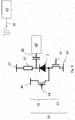
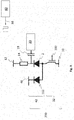
- Figure 6 represents a control circuit 130 according to a first embodiment for controlling the avalanche diode 2 of Figure 1 .
- the control circuit 130 is identical to the control circuit 30 of Figure 3 except that the PMOS transistor 44 is replaced by a clamp diode 102.
- the clamp diode may be any diode, for example a small PN diode.
- the clamp diode 102 is less voluminous than the PMOS transistor 44 and therefore the size of the control circuit 130 can be reduced. More specifically, the cathode of the clamp diode 102 is connected to the supply voltage 46.
- the anode of the clamp diode 102 is connected to the anode of the avalanche diode 2.
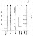
- Figure 7 illustrates the behaviour of the avalanche diode 2 of Figure 1 when controlled by the control circuit 130 of Figure 6 .
- the switch 34 connects the anode of the avalanche diode 2 to the supply voltage 10. In this way, the reverse bias voltage is set above the breakdown voltage.
- the clamp diode 102 is not conducting (i.e. the voltage between the cathode and the anode of the clamp diode 102 is below a threshold) and disconnects the anode of the avalanche diode 2 from the supply voltage 46.
- a first photon 702 is absorbed by the avalanche diode 2 an avalanche is generated.
- the reverse current flowing through the avalanche diode 2 (and through the switch 34) increases sharply during the avalanche (i.e. the recombination of electrons and holes in the depletion region increases sharply).
- the reverse current then becomes nil when the reverse bias voltage drops below the breakdown voltage.
- the recharge current flowing through the resistor 14 is approximately nil during the avalanche.
- the recharge current increases sharply when the reverse bias voltage drops below the breakdown voltage.
- the recharge current exponentially decreases until being approximately nil when the reverse bias voltage is reset above the breakdown voltage.
- the detector 20 detects the sharp increase in the reverse current and generates an output (e.g. a pulse). That is, after detecting the first photon the avalanche diode 2 is reset (i.e. quenched) by the resistor 14 to detect a second photon 704.
- the reverse current flowing through the avalanche diode 2 increases sharply during the avalanche (i.e. the recombination of electrons and holes in the depletion region increases sharply).
- the reverse current then becomes nil when the reverse bias voltage drops below the breakdown voltage.
- the recharge current flowing through the resistor 14 is approximately nil during the avalanche.
- the recharge current increases sharply when the reverse bias voltage drops below the breakdown voltage.
- the recharge current exponentially decreases until being approximately nil when the reverse bias voltage is reset above the breakdown voltage.
- the detector 20 detects the sharp increase in the reverse current and generates a corresponding output (e.g. a pulse). That is, after detecting the second photon the avalanche diode 2 is reset (i.e. quenched) by the resistor 14 to detect a third photon 706.
- the switch 34 disconnects the anode of the avalanche diode 2 from the supply voltage 10. In this way, the reverse bias voltage is left floating above the breakdown voltage.
- the clamp diode 102 is nonconducting (i.e. the voltage between the cathode and the anode of the clamp diode 102 is below the threshold) and disconnects the anode of the avalanche diode 2 to the supply voltage 46.
- the third photon 706 When the third photon 706 is absorbed by the avalanche diode 2 an avalanche is generated.
- the reverse current flowing through the avalanche diode 2 increases sharply during the avalanche (i.e. the recombination of electrons and holes in the depletion region increases sharply).
- the reverse current then becomes nil when the reverse bias voltage drops below the breakdown voltage.
- the recharge current flowing through the resistor 14 is approximately nil during the avalanche and remains approximately when the reverse bias voltage drops below the breakdown voltage.
- the detector 20 detects the sharp increase in the reverse current and generates a corresponding output (e.g. a pulse). That is, after detecting the third photon 706 the avalanche diode 2 is disabled and a fourth photon 708 cannot be detected.
- the clamp diode 102 starts conducting (i.e. the voltage between the cathode and the anode of the clamp diode 102 is above the threshold) and connects the anode of the avalanche diode 2 to the supply voltage 46.
- the anode of the avalanche diode 2 is maintained approximatively at the supply voltage 46 (i.e. supply voltage 46 minus the threshold) and the reverse bias voltage is maintained below the breakdown voltage.
- the fourth photon 708 When the fourth photon 708 is absorbed by the avalanche diode 2 no avalanche is generated because the reverse bias voltage is below the breakdown voltage.
- the reverse current flowing through the avalanche diode 2 is approximately nil.
- the recharge current flowing through the resistor 14 is approximately nil.
- the reverse bias voltage is below the breakdown voltage.
- the detector 20 does not detect any sharp increase in the reverse current and generates a corresponding output (e.g. no pulse).
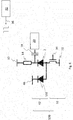
- Figure 8 represents a control circuit 230 according to a second embodiment for controlling the avalanche diode 2 of Figure 1 .
- the control circuit 230 is identical to the control circuit 130 of Figure 6 except that the NMOS transistor 44 is replaced by a high voltage NMOS transistor 202, such as an N EDMOS transistor.
- Figure 9 represents a control circuit 330 according to a third embodiment for controlling the avalanche diode 2 of Figure 1 when reverse biased with a cathode moving node.
- the control circuit 330 is identical to the control circuit 130 of Figure 6 except that the active pull down module 32 includes a cascode arrangement.
- the cascode active pull down module 32 includes the N MOS transistor 34 and an N MOS transistor 302. More specifically, the drain of the N MOS transistor 34 is connected to the source of the N MOS transistor 302. The source of the N MOS transistor 34 is connected to the voltage supply 10. The drain of the N MOS transistor 302 is connected to the anode of the avalanche diode 2. The gate of the N MOS transistor 34 is arranged to receive the control signal 36. The gate of the N MOS transistor 302 is arranged to receive a control signal 304 generated by a control signal generator 306. Here, the control signal 304 is fixed (i.e. not alternating). In this way, the N MOS transistor 302 protects the N MOS transistor 34 from a potentially too high drain source voltage.
- control signal 304 may be modulated (i.e. alternating) so that the N MOS transistor 302 may selectively connect the anode of the avalanche diode 2 to the supply voltage 10.
- FIG 10 represents a control circuit 430 according to a fourth embodiment for controlling the avalanche diode 2 of Figure 1 .
- the control circuit 430 is identical to the control circuit 330 of Figure 9 except that the cascode arrangement is formed by the N MOS transistor 34 and a high voltage N MOS transistor, such as an N EDMOS transistor 402.
- the drain of the N MOS transistor 34 is connected to the source of the N EDMOS transistor 402.
- the source of the MOS transistor 34 is connected to the voltage supply 10.
- the drain of the N MOS transistor 402 is connected to the anode of the avalanche diode 2.
- the gate of the N MOS transistor 34 is arranged to receive the control signal 36.
- the gate of the N MOS transistor 402 is arranged to receive a control signal 404 generated by a control signal generator 406.
- the control signal 404 is fixed (i.e. not alternating). In this way, the N EDMOS transistor 402 protects the N MOS transistor 34 from a potentially too high drain source voltage.
Landscapes
- Physics & Mathematics (AREA)
- General Physics & Mathematics (AREA)
- Spectroscopy & Molecular Physics (AREA)
- Electronic Switches (AREA)
- Semiconductor Integrated Circuits (AREA)
Abstract
Description
- The present disclosure relates to a control circuit, in particular a control circuit for controlling an avalanche diode, and a method of operating the control circuit.
- Existing single photon avalanche diodes (SPADs) are based on a PN junction. The PN junction is reverse biased at a voltage exceeding a breakdown voltage. In this way, a carrier generated by a single photon can be injected into a depletion region and can cause a self-sustaining avalanche. The SPAD may be quenched allowing the PN junction to be reset to detect further photons.
- According to one aspect, there is provided a control circuit, comprising: at least one active module designed to enable an avalanche diode; and at least one passive module designed to disable the avalanche diode
- The at least one active module may be designed to set a reverse bias voltage above or at a breakdown voltage.
- The at least one passive module may designed to set the reverse bias voltage below the breakdown voltage
- The at least one passive module may include at least one clamp diode arranged to connect a supply voltage to an electrode of the avalanche terminal.
- The at least one clamp diode may include a cathode connected to the supply voltage and an anode connected to an anode of the avalanche diode.
- The at least one active module may include at least one first switch controlled by at least one first control signal to connect and disconnect an electrode of the avalanche diode to a voltage supply.
- The at least one first switch may be a metal-oxide-semiconductor, MOS, switch.
- The at least one first switch may be an N type metal-oxide-semiconductor, NMOS, switch.
- The at least one first switch may be an N type extended drain metal-oxide-semiconductor, NEDMOS, switch.
- The at least one active module may include at least one second switch controlled by at least one second control signal to connect and disconnect an electrode of the avalanche diode to the voltage supply.
- The at least one second switch may be a metal-oxide-semiconductor, MOS, switch.
- The at least one second switch may be an N type metal-oxide-semiconductor, NMOS, switch.
- The at least one second switch may be an N type extended drain metal-oxide-semiconductor, NEDMOS, switch.
- The at least one first switch and the at least one second switch may be connected in a cascode arrangement.
- A drain of the at least one first switch may be connected to the source of the at least one second switch.
- A source of the at least one first switch is connected to the voltage supply.
- A drain of the at least one second switch may be connected to the anode of the avalanche diode.
- A gate of the at least one first switch may be arranged to receive the first control signal.
- A gate of the at least one second switch may be arranged to receive the second control signal.
- The avalanche diode may be an avalanche photodiode.
- The avalanche diode may be a single photo avalanche diode (SPAD),
- According to a second aspect there is provided a system, comprising: an avalanche diode; and a control circuit comprising: at least one active module designed to enable an avalanche diode; and at least one passive module designed to disable the avalanche diode
- The at least one active module may be designed to set a reverse bias voltage above or at a breakdown voltage.
- The at least one passive module may designed to set the reverse bias voltage below the breakdown voltage
- The at least one passive module may include at least one clamp diode arranged to connect a supply voltage to an electrode of the avalanche terminal.
- The at least one clamp diode may include a cathode connected to the supply voltage and an anode connected to an anode of the avalanche diode.
- The at least one active module may include at least one first switch controlled by at least one first control signal to connect and disconnect an electrode of the avalanche diode to a voltage supply.
- The at least one first switch may be a metal-oxide-semiconductor, MOS, switch.
- The at least one first switch may be an N type metal-oxide-semiconductor, NMOS, switch.
- The at least one first switch may be an N type extended drain metal-oxide-semiconductor, NEDMOS, switch.
- The at least one active module may include at least one second switch controlled by at least one second control signal to connect and disconnect an electrode of the avalanche diode to the voltage supply.
- The at least one second switch may be a metal-oxide-semiconductor, MOS, switch.
- The at least one second switch may be an N type metal-oxide-semiconductor, NMOS, switch.
- The at least one second switch may be an N type extended drain metal-oxide-semiconductor, NEDMOS, switch.
- The at least one first switch and the at least one second switch may be connected in a cascode arrangement.
- A drain of the at least one first switch may be connected to the source of the at least one second switch.
- A source of the at least one first switch is connected to the voltage supply.
- A drain of the at least one second switch may be connected to the anode of the avalanche diode.
- A gate of the at least one first switch may be arranged to receive the first control signal.
- A gate of the at least one second switch may be arranged to receive the second control signal.
- The avalanche diode may be an avalanche photodiode.
- The avalanche diode may be a single photo avalanche diode (SPAD),
- The system may be an imaging sensor.
- According to a third aspect, there is provided a method of operating a control circuit comprising: operating at least one active module designed to enable an avalanche diode; and operating at least one passive module designed to disable the avalanche diode.
- The at least one active module may be designed to set a reverse bias voltage above or at a breakdown voltage.
- The at least one passive module may designed to set the reverse bias voltage below the breakdown voltage
- The at least one passive module may include at least one clamp diode arranged to connect a supply voltage to an electrode of the avalanche terminal.
- The at least one clamp diode may include a cathode connected to the supply voltage and an anode connected to an anode of the avalanche diode.
- The at least one active module may include at least one first switch controlled by at least one first control signal to connect and disconnect an electrode of the avalanche diode to a voltage supply.
- The at least one first switch may be a metal-oxide-semiconductor, MOS, switch.
- The at least one first switch may be an N type metal-oxide-semiconductor, NMOS, switch.
- The at least one first switch may be an N type extended drain metal-oxide-semiconductor, NEDMOS, switch.
- The at least one active module may include at least one second switch controlled by at least one second control signal to connect and disconnect an electrode of the avalanche diode to the voltage supply.
- The at least one second switch may be a metal-oxide-semiconductor, MOS, switch.
- The at least one second switch may be an N type metal-oxide-semiconductor, NMOS, switch.
- The at least one second switch may be an N type extended drain metal-oxide-semiconductor, NEDMOS, switch.
- The at least one first switch and the at least one second switch may be connected in a cascode arrangement.
- A drain of the at least one first switch may be connected to the source of the at least one second switch.
- A source of the at least one first switch is connected to the voltage supply.
- A drain of the at least one second switch may be connected to the anode of the avalanche diode.
- A gate of the at least one first switch may be arranged to receive the first control signal.
- A gate of the at least one second switch may be arranged to receive the second control signal.
- The avalanche diode may be an avalanche photodiode.
- The avalanche diode may be a single photo avalanche diode (SPAD),
- Reference will now be made, by way of example only, to the accompanying drawings in which:
-
Figure 1 shows a cross-section of an avalanche diode; -
Figure 2a shows the avalanche diode ofFigure 1 when reverse biased with an anode moving node; -
Figure 2b shows the avalanche diode ofFigure 1 when reverse biased with a cathode moving node; -
Figure 3 shows a control circuit for controlling the avalanche diode ofFigure 1 ; -
Figure 4 shows a graph illustrating the behaviour of the avalanche diode ofFigure 1 when controlled by the control circuit ofFigure 3 ; -
Figure 5 shows another control circuit for controlling the avalanche diode ofFigure 1 ; -
Figure 6 shows a control circuit for controlling the avalanche diode ofFigure 1 according to a first embodiment; -
Figure 7 shows a graph illustrating the behaviour of the avalanche diode ofFigure 1 a when controlled by the control circuit ofFigure 3 ; -
Figure 8 shows a control circuit for controlling the avalanche diode ofFigure 1 according to a second embodiment; -
Figure 9 shows a control circuit for controlling the avalanche diode ofFigure 1 according to a third embodiment; and -
Figure 10 shows a control circuit for controlling the avalanche diode ofFigure 1 according to a fourth embodiment. - A diode is an electrical device allowing current to move through it in one direction with far greater ease than in the other. The most common kind of diode in modern circuit design is the semiconductor diode and is based on a PN junction.
- A PN junction includes a P region (i.e. region doped with a P dopant) and an N region (i.e. region doped with an N dopant type). The N region contains electrons in excess while the P region contains holes in excess. When the PN junction is formed holes are naturally diffused from the P region to the N region and recombined with electrons. Likewise, electrons are naturally diffused from the N region to the P region and are recombined with holes. In this way, a depletion region with pairs of recombined holes and electrons is formed at the interface (i.e. the junction) of the P region and the N region.
- The diffusion of holes from the P region leaves negative acceptor ions in the P region while the diffusion of electrons from the N region leaves positive donor ions in the N region. This creates a depletion region electric field that provides a force opposing the continued diffusion of holes and electrons. When the depletion region electric field is sufficiently high the diffusion of holes and electrons is interrupted and the depletion region reaches an equilibrium.
- The width of the depletion region depends on the concentration of holes in the P region, the concentration of electrons in the N region and a voltage supply applied to the PN junction.
- When the voltage supply is a forward bias voltage supply, the P region is connected with a positive terminal of the voltage supply and the N region is connected with a negative terminal of the voltage supply. In this way, the holes in the P region and the electrons in the N region are pushed toward the interface of the P region and the N region. The width of the depletion region decreases.
- When the voltage supply is a reverse bias voltage supply, the P region is connected with a negative terminal of the voltage supply and the N region is connected with a positive terminal of the voltage supply. In this way, the holes in the P region and the electrons in the N region are pushed away from the interface of the P region and the N region. The width of the depletion region increases.
- The width of the depletion region increases with the increase in reverse bias voltage supply up to a voltage. If the reverse bias voltage supply is increased beyond that voltage, the junction breaks down and allows a reverse current. At this point, a small increase in the voltage will rapidly increase the reverse current. The voltage at which the PN junction breaks down occurs is known as the "breakdown voltage".
- The depletion region breakdown may be caused by two mechanisms: zener breakdown and avalanche breakdown.
- In avalanche breakdown, when the reverse voltage supply exceeds the breakdown voltage, electrons diffused in the depletion region are accelerated. The electrons collide with atoms and free bound electrons. Some of these electrons recombine with holes. Others are accelerated in the depletion region, collide with atoms and free further bound electrons, and so on. Likewise, holes diffused in the depletion region area are accelerated in the opposite direction and initiate a similar process. In this way, a self-sustaining avalanche is created and the reverse current increases.
- An avalanche diode, such as a single photon avalanche detectors (SPAD), follows the above principle. The PN junction is reverse biased at a voltage exceeding the breakdown voltage. When a photon with sufficient energy is absorbed, a bound electron is freed in the depletion region. The electron is accelerated, collide with atoms and frees further bound electrons. Some of these electrons recombine with holes. Others are accelerated, collide with atoms and free further bound electron, and so on. Likewise, holes diffused in the depletion region area are accelerated in the opposite direction and initiate a similar process. In this way, a self-sustaining avalanche is created and the reverse current increases. The avalanche can be stopped by setting the reverse bias voltage supply below the breakdown voltage.
-
Figure 1 represents anavalanche diode 2, for example a single photon avalanche diode (SPAD) implemented as part of a back side illuminated light detector. Theavalanche diode 2 may typically be integrated in a system such as an imaging sensor. - The
avalanche diode 2 comprises aPN junction 4 including a P region 6 (i.e. a region doped with a P dopant) and an N region 8 (i.e. a region doped with an N dopant). In an implementation, theP region 6 is an epitaxial layer of P dopant type grown on a Silicon substrate (not represented) and theN region 8 is a well of N dopant type formed within the epitaxial layer. Here, theN region 8 is centred (i.e. aligned with a central longitudinal axis). ThePN junction 4 comprises a depletion region (also known as depletion layer or depletion zone) that is naturally formed at the interface (i.e. junction) of theP region 6 and theN region 8 as described above. - The
avalanche diode 2 comprises an anode (not represented) connecting theP region 6 to a negative terminal of avoltage supply 10 and a cathode (not represented) connecting theN region 8 to a positive terminal of thevoltage supply 12. - The
avalanche diode 2 advantageously comprises atrench isolation region 22 surrounding thePN junction 4 to prevent current leakage from/ toward adjacent semiconductor device components. Thetrench isolation region 12 is for example made of Silicon Dioxide (SiO2). - The
avalanche diode 2 shown inFigure 1 is a back side illuminated avalanche diode so that the amount of light captured can be increased and low-light performance can be improved. As discussed above, when a photon with sufficient energy is absorbed via the back side, a bound electron is freed in the depletion region, accelerated, collides with atoms and free further bound electrons. Some of these electrons recombine with holes. Others are accelerated in, collide with atoms and free further bound electrons, and so on. -
Figure 2a shows theavalanche diode 2 ofFigure 1 when reverse biased with an anode moving node. The cathode of theavalanche diode 2 is directly connected to thesupply voltage 12. The anode of theavalanche diode 2 is indirectly connected to thesupply voltage 10 via aresistor 14. Furthermore, the anode of theavalanche diode 2 is indirectly connected to adetection module 20 via acapacitor 18. Thedetection module 20 can include a comparator (not represented) arranged to output a determined value (e.g. pulse or no pulse) when the reverse current flowing through thediode 2 is above a threshold. A comparator can for example be implemented by cascading two complementary metal-oxide-semiconductor (CMOS) inverters. -
Figure 2b shows theavalanche diode 2 ofFigure 1 when reverse biased with a cathode moving node. The anode of theavalanche diode 2 is directly connected to thesupply voltage 10. The cathode of theavalanche diode 2 is indirectly connected to thesupply voltage 12 via theresistor 14. Furthermore, the cathode of theavalanche diode 2 is indirectly connected to thedetection module 20 via thecapacitor 18. This configuration is safer and therefore preferred. - Indeed, in this arrangement the cathode of the
avalanche diode 2 may be at a high voltage (e.g. >10V). This is beyond the limits of standard MOSFETs in modern CMOS processes. Also, when the avalanche is triggered, the cathode voltage swing will be equal to the excess bias voltage. It is common for SPADs (especially depleted SPADs) to operate with large excess bias voltages in excess of the voltage range of a standard MOSFET. In this case, the coupling capacitor may be sized such that the pulse at thedetection module 20 is attenuated to within the acceptable voltage range. - In the following disclosure various control circuits will be described for controlling the
avalanche diode 2 ofFigure 1 when reverse biased with a cathode moving node as shown onFigure 2b . However, it will be understood that these control circuits can equally be used for controlling theavalanche diode 2 ofFigure 1 when reverse biased with an anode moving node as shown onFigure 2a . -
Figure 3 represents acontrol circuit 30 for controlling theavalanche diode 2 ofFigure 1 . Here, thecontrol circuit 30 is formed by a CMOS device. - The
control circuit 30 comprises an active pull downmodule 32 designed to set the reverse bias voltage above or at a breakdown voltage and therefore enable theavalanche diode 2. The active pull downmodule 32 in other words is configured to selectively pull down the potential of the anode of theavalanche diode 2. The active pull downmodule 32 includes aswitch 34 controlled by acontrol signal 36 to connect and disconnect the anode of theavalanche diode 2 to thevoltage supply 10. Here, theswitch 34 is formed by an N channel metal-oxide-semiconductor (NMOS) transistor. The NMOS transistor includes a drain connected to the anode of theavalanche diode 2, a source connected tovoltage supply 10 and a gate connected to acontrol signal generator 40 providing thecontrol signal 36. Thecontrol signal 36 may be a square wave signal that alternates between a high potential and a low potential. - The
control circuit 30 comprises an active pull upmodule 42 designed to set the reverse bias voltage below the breakdown voltage and therefore disable the avalanche diode. The active pull upmodule 42 in other words is configured to selectively pull up the potential of the anode of theavalanche diode 2. The active pull upmodule 42 includes aswitch 44 controlled by thecontrol signal 36 to connect and disconnect the anode of theavalanche diode 2 to avoltage supply 46. Here, theswitch 34 is formed by a P channel metal-oxide-semiconductor (PMOS) transistor. The PMOS transistor includes a drain connected to the anode of theavalanche diode 2, a source connected tovoltage supply 46 and a gate connected to thecontrol signal generator 40 providing thecontrol signal 36. -
Figure 4 illustrates the behaviour of theavalanche diode 2 ofFigure 1 when controlled by thecontrol circuit 30 ofFigure 3 . - When the
control signal 36 switches to the high potential theswitch 34 connects the anode of theavalanche diode 2 to thesupply voltage 10. Theswitch 44 disconnects the anode of theavalanche diode 2 from thesupply voltage 46. In this way, the reverse bias voltage may be set above the breakdown voltage. - When a
first photon 402 is absorbed by theavalanche diode 2 an avalanche is generated as discussed above. The reverse current flowing through theavalanche diode 2 increases sharply during the avalanche (i.e. the recombination of electrons and holes in the depletion region increases sharply). The reverse current then becomes nil when the reverse bias voltage drops below the breakdown voltage. By contrast, the recharge current flowing through theresistor 14 is approximately nil during the avalanche. The recharge current increases sharply when the reverse bias voltage drops below the breakdown voltage. The recharge current exponentially decreases until being approximately nil when the reverse bias voltage is reset above the breakdown voltage. Thedetector 20 detects the sharp increase in the reverse current and generates an output (e.g. a pulse). That is, after detecting thefirst photon 402 theavalanche diode 2 is reset (i.e. quenched) by theresistor 14 to detect asecond photon 404. - When the
second photon 404 is absorbed, another avalanche is generated. Again, the reverse current flowing through theavalanche diode 2 increases sharply during the avalanche (i.e. the recombination of electrons and holes in the depletion region increases sharply). The reverse current is then approximately nil when the reverse bias voltage drops below the breakdown voltage. By contrast, the recharge current flowing through theresistor 14 is approximately nil during the avalanche. The recharge current increases sharply when the reverse bias voltage drops below the breakdown voltage. The recharge current exponentially decreases until being approximately nil when the reverse bias voltage is reset above the breakdown voltage. Thedetector 20 detects the sharp increase in the reverse current and generates a corresponding output (e.g. a pulse). That is, after detecting thesecond photon 404 theavalanche diode 2 is reset (i.e. quenched) by theresistor 14 to detect athird photon 406. - When the
control signal 36 switches to the low potential, theswitch 34 disconnects the anode of theavalanche diode 2 from thesupply voltage 10. Theswitch 46 connects the anode of theavalanche diode 2 to thesupply voltage 46. In this way, the reverse bias voltage is pulled below the breakdown voltage by thevoltage supply 46. - When the
third photon 406 is absorbed by theavalanche diode 2 no avalanche is generated because the reverse bias voltage is below the breakdown voltage. The reverse current flowing through theavalanche diode 2 is approximately nil. The recharge current flowing through theresistor 14 is approximately nil. Thedetector 20 does not detect any sharp increase in the reverse current and generates a corresponding output (e.g. no pulse). -
Figure 5 represents a control circuit 60 for controlling theavalanche diode 2 ofFigure 1 . Thecontrol circuit 50 is identical to thecontrol circuit 30 ofFigure 3 except that the active pull downmodule 32 and the active pull upmodule 42 include cascode arrangements. - The active pull down
module 32 includes theN MOS transistor 34 and anN MOS transistor 35. More specifically, the drain of theN MOS transistor 34 is connected to the source of theN MOS transistor 35. The source of theMOS transistor 34 is connected to thevoltage supply 10. The drain of theN MOS transistor 35 is connected to the anode of theavalanche diode 2. The gate of theN MOS transistor 34 is arranged to receive thecontrol signal 36. The gate of theN MOS transistor 35 is arranged to receive a control signal 37 generated by acontrol signal generator 41. Here, thecontrol signal 304 is fixed (i.e. not alternating). In this way, theN MOS transistor 35 protects theN MOS transistor 34 from a potentially too high drain source voltage. - Likewise, the active pull up
module 42 includes theP MOS transistor 44 and aP MOS transistor 45. More specifically, the drain of theP MOS transistor 45 is connected to the source of theP MOS transistor 44. The source of theMOS transistor 45 is connected to thevoltage supply 12. The drain of theP MOS transistor 44 is connected to the anode of theavalanche diode 2. The gate of theN MOS transistor 44 is arranged to receive thecontrol signal 36. The gate of theP MOS transistor 45 is arranged to receive the control signal 37. In this way, theP MOS transistor 45 protects theP MOS transistor 44 from a potentially too high drain source voltage. - A problem with CMOS devices is that they have large area requirements. In particular, the PMOS transistor of a CMOS device will occupy significant layout space due to nanowires. A possible replacement for the PMOS transistor could be a P drift transistor or a P extended drain metal-oxide-semiconductor (EDMOS) transistor, but these transistors are also voluminous.
-
Figure 6 represents acontrol circuit 130 according to a first embodiment for controlling theavalanche diode 2 ofFigure 1 . Thecontrol circuit 130 is identical to thecontrol circuit 30 ofFigure 3 except that thePMOS transistor 44 is replaced by aclamp diode 102. The clamp diode may be any diode, for example a small PN diode. Theclamp diode 102 is less voluminous than thePMOS transistor 44 and therefore the size of thecontrol circuit 130 can be reduced. More specifically, the cathode of theclamp diode 102 is connected to thesupply voltage 46. The anode of theclamp diode 102 is connected to the anode of theavalanche diode 2. -
Figure 7 illustrates the behaviour of theavalanche diode 2 ofFigure 1 when controlled by thecontrol circuit 130 ofFigure 6 . - When the
control signal 36 switches to the high potential, theswitch 34 connects the anode of theavalanche diode 2 to thesupply voltage 10. In this way, the reverse bias voltage is set above the breakdown voltage. Theclamp diode 102 is not conducting (i.e. the voltage between the cathode and the anode of theclamp diode 102 is below a threshold) and disconnects the anode of theavalanche diode 2 from thesupply voltage 46. - When a
first photon 702 is absorbed by theavalanche diode 2 an avalanche is generated. The reverse current flowing through the avalanche diode 2 (and through the switch 34) increases sharply during the avalanche (i.e. the recombination of electrons and holes in the depletion region increases sharply). The reverse current then becomes nil when the reverse bias voltage drops below the breakdown voltage. By contrast, the recharge current flowing through theresistor 14 is approximately nil during the avalanche. The recharge current increases sharply when the reverse bias voltage drops below the breakdown voltage. The recharge current exponentially decreases until being approximately nil when the reverse bias voltage is reset above the breakdown voltage. Thedetector 20 detects the sharp increase in the reverse current and generates an output (e.g. a pulse). That is, after detecting the first photon theavalanche diode 2 is reset (i.e. quenched) by theresistor 14 to detect asecond photon 704. - When the
second photon 704 is absorbed, another avalanche is generated. Again, the reverse current flowing through theavalanche diode 2 increases sharply during the avalanche (i.e. the recombination of electrons and holes in the depletion region increases sharply). The reverse current then becomes nil when the reverse bias voltage drops below the breakdown voltage. By contrast, the recharge current flowing through theresistor 14 is approximately nil during the avalanche. The recharge current increases sharply when the reverse bias voltage drops below the breakdown voltage. The recharge current exponentially decreases until being approximately nil when the reverse bias voltage is reset above the breakdown voltage. Thedetector 20 detects the sharp increase in the reverse current and generates a corresponding output (e.g. a pulse). That is, after detecting the second photon theavalanche diode 2 is reset (i.e. quenched) by theresistor 14 to detect athird photon 706. - When the
control signal 36 switches to its low potential, theswitch 34 disconnects the anode of theavalanche diode 2 from thesupply voltage 10. In this way, the reverse bias voltage is left floating above the breakdown voltage. Theclamp diode 102 is nonconducting (i.e. the voltage between the cathode and the anode of theclamp diode 102 is below the threshold) and disconnects the anode of theavalanche diode 2 to thesupply voltage 46. - When the
third photon 706 is absorbed by theavalanche diode 2 an avalanche is generated. The reverse current flowing through theavalanche diode 2 increases sharply during the avalanche (i.e. the recombination of electrons and holes in the depletion region increases sharply). The reverse current then becomes nil when the reverse bias voltage drops below the breakdown voltage. By contrast, the recharge current flowing through theresistor 14 is approximately nil during the avalanche and remains approximately when the reverse bias voltage drops below the breakdown voltage. Thedetector 20 detects the sharp increase in the reverse current and generates a corresponding output (e.g. a pulse). That is, after detecting thethird photon 706 theavalanche diode 2 is disabled and afourth photon 708 cannot be detected. - It will be understood that as the reverse bias voltage decreases and reaches a voltage below the breakdown voltage, the
clamp diode 102 starts conducting (i.e. the voltage between the cathode and the anode of theclamp diode 102 is above the threshold) and connects the anode of theavalanche diode 2 to thesupply voltage 46. In this way, the anode of theavalanche diode 2 is maintained approximatively at the supply voltage 46 (i.e.supply voltage 46 minus the threshold) and the reverse bias voltage is maintained below the breakdown voltage. - When the
fourth photon 708 is absorbed by theavalanche diode 2 no avalanche is generated because the reverse bias voltage is below the breakdown voltage. The reverse current flowing through theavalanche diode 2 is approximately nil. The recharge current flowing through theresistor 14 is approximately nil. The reverse bias voltage is below the breakdown voltage. Thedetector 20 does not detect any sharp increase in the reverse current and generates a corresponding output (e.g. no pulse). -
Figure 8 represents acontrol circuit 230 according to a second embodiment for controlling theavalanche diode 2 ofFigure 1 . Thecontrol circuit 230 is identical to thecontrol circuit 130 ofFigure 6 except that theNMOS transistor 44 is replaced by a highvoltage NMOS transistor 202, such as an N EDMOS transistor. - It will be understood that the behaviour of the
avalanche diode 2 ofFigure 1 when controlled by thecontrol circuit 230 ofFigure 8 is the same as when controlled by thecontrol circuit 130 ofFigure 6 . Accordingly, this behaviour of the avalanche diode 2is not discussed in further details. -
Figure 9 represents acontrol circuit 330 according to a third embodiment for controlling theavalanche diode 2 ofFigure 1 when reverse biased with a cathode moving node. Thecontrol circuit 330 is identical to thecontrol circuit 130 ofFigure 6 except that the active pull downmodule 32 includes a cascode arrangement. - The cascode active pull down
module 32 includes theN MOS transistor 34 and anN MOS transistor 302. More specifically, the drain of theN MOS transistor 34 is connected to the source of theN MOS transistor 302. The source of theN MOS transistor 34 is connected to thevoltage supply 10. The drain of theN MOS transistor 302 is connected to the anode of theavalanche diode 2. The gate of theN MOS transistor 34 is arranged to receive thecontrol signal 36. The gate of theN MOS transistor 302 is arranged to receive acontrol signal 304 generated by acontrol signal generator 306. Here, thecontrol signal 304 is fixed (i.e. not alternating). In this way, theN MOS transistor 302 protects theN MOS transistor 34 from a potentially too high drain source voltage. - It will be noted that alternatively the
control signal 304 may be modulated (i.e. alternating) so that theN MOS transistor 302 may selectively connect the anode of theavalanche diode 2 to thesupply voltage 10. - It will be understood that the behaviour of the
avalanche diode 2 ofFigure 1 when controlled by thecontrol circuit 330 ofFigure 9 is the same as when controlled by thecontrol circuit 130 ofFigure 6 . Accordingly, this behaviour of the avalanche diode 2is not discussed in further details. -
Figure 10 represents acontrol circuit 430 according to a fourth embodiment for controlling theavalanche diode 2 ofFigure 1 . Thecontrol circuit 430 is identical to thecontrol circuit 330 ofFigure 9 except that the cascode arrangement is formed by theN MOS transistor 34 and a high voltage N MOS transistor, such as anN EDMOS transistor 402. - More specifically, the drain of the
N MOS transistor 34 is connected to the source of theN EDMOS transistor 402. The source of theMOS transistor 34 is connected to thevoltage supply 10. The drain of theN MOS transistor 402 is connected to the anode of theavalanche diode 2. The gate of theN MOS transistor 34 is arranged to receive thecontrol signal 36. The gate of theN MOS transistor 402 is arranged to receive acontrol signal 404 generated by acontrol signal generator 406. Here, thecontrol signal 404 is fixed (i.e. not alternating). In this way, theN EDMOS transistor 402 protects theN MOS transistor 34 from a potentially too high drain source voltage. - It will be understood that the behaviour of the
avalanche diode 2 ofFigure 1 when controlled by thecontrol circuit 430 ofFigure 10 is the same as when controlled by thecontrol circuit 130 ofFigure 6 . Accordingly, this behaviour of the avalanche diode 2is not discussed in further details. - Various embodiments with different variations have been described here above. It should be noted that those skilled in the art may combine various elements of these various embodiments and variations.
- Such alterations, modifications, and improvements are intended to be part of this disclosure, and are intended to be within the scope of the claims. Accordingly, the foregoing description is by way of example only and is not intended to be limiting. The invention is limited only as defined in the claims and the equivalents thereto.
Claims (15)
- A control circuit, comprising:at least one active module designed to enable an avalanche diode; andat least one passive module designed to disable the avalanche diode.
- The control circuit of claim 1, wherein the at least one active module is designed to set a reverse bias voltage above or at a breakdown voltage.
- The control circuit of any one of claims 1 and 2, wherein the at least one passive module is designed to set the reverse bias voltage below the breakdown voltage
- The control circuit of any one of claims 1 to 3, wherein the at least one passive module includes at least one clamp diode arranged to connect a supply voltage to an electrode of the avalanche terminal.
- The control circuit of claim 4, wherein the at least one clamp diode includes a cathode connected to the supply voltage and an anode connected to an anode of the avalanche diode.
- The control circuit of any one of claims 1 to 5, wherein the at least one active module includes at least one first switch controlled by at least one first control signal to connect and disconnect an electrode of the avalanche diode to a voltage supply.
- The control circuit of claim 6, wherein the at least one first switch is a metal-oxide-semiconductor, MOS, switch.
- The control circuit of claim 7, wherein the at least one first switch is an N type metal-oxide-semiconductor, NMOS, switch.
- The control circuit of claim 8, wherein the at least one first switch is an N type extended drain metal-oxide-semiconductor, NEDMOS, switch.
- The control circuit of any one of claims 6 to 9, wherein the at least one active module includes at least one second switch controlled by at least one second control signal to connect and disconnect an electrode of the avalanche diode to the voltage supply.
- The control circuit of claim 10, wherein the at least one second switch is a metal-oxide-semiconductor, MOS, switch.
- The control circuit of claim 11, wherein the at least one second switch is an N type metal-oxide-semiconductor, NMOS, switch
- The control circuit of claim 12, wherein the at least one second switch is an N type extended drain metal-oxide-semiconductor, NEDMOS, switch.
- A system, comprising:an avalanche diode; anda control circuit according to any one of claims 1 to 13.
- A method of operating a control circuit comprising:operating at least one active module designed to enable an avalanche diode; andoperating at least one passive module designed to disable the avalanche diode.
Priority Applications (4)
| Application Number | Priority Date | Filing Date | Title |
|---|---|---|---|
| EP17198338.0A EP3477707B1 (en) | 2017-10-25 | 2017-10-25 | Control circuit and method of operating a control circuit |
| US16/157,882 US11031511B2 (en) | 2017-10-25 | 2018-10-11 | Control circuit and method of operating a control circuit |
| CN201821727987.7U CN209182668U (en) | 2017-10-25 | 2018-10-24 | Control Circuits and Control Systems |
| CN201811244951.8A CN109709825B (en) | 2017-10-25 | 2018-10-24 | Control circuit and method of operating a control circuit |
Applications Claiming Priority (1)
| Application Number | Priority Date | Filing Date | Title |
|---|---|---|---|
| EP17198338.0A EP3477707B1 (en) | 2017-10-25 | 2017-10-25 | Control circuit and method of operating a control circuit |
Publications (2)
| Publication Number | Publication Date |
|---|---|
| EP3477707A1 true EP3477707A1 (en) | 2019-05-01 |
| EP3477707B1 EP3477707B1 (en) | 2021-05-05 |
Family
ID=60182487
Family Applications (1)
| Application Number | Title | Priority Date | Filing Date |
|---|---|---|---|
| EP17198338.0A Active EP3477707B1 (en) | 2017-10-25 | 2017-10-25 | Control circuit and method of operating a control circuit |
Country Status (3)
| Country | Link |
|---|---|
| US (1) | US11031511B2 (en) |
| EP (1) | EP3477707B1 (en) |
| CN (2) | CN109709825B (en) |
Cited By (1)
| Publication number | Priority date | Publication date | Assignee | Title |
|---|---|---|---|---|
| EP4117043A1 (en) * | 2021-07-08 | 2023-01-11 | STMicroelectronics (Research & Development) Limited | Linear regulation of spad shutoff voltage |
Families Citing this family (13)
| Publication number | Priority date | Publication date | Assignee | Title |
|---|---|---|---|---|
| US10720913B1 (en) | 2019-05-28 | 2020-07-21 | Infineon Technologies Austria Ag | Integrated failsafe pulldown circuit for GaN switch |
| US10958268B1 (en) | 2019-09-04 | 2021-03-23 | Infineon Technologies Austria Ag | Transformer-based driver for power switches |
| US11162839B2 (en) | 2019-12-12 | 2021-11-02 | Stmicroelectronics (Research & Development) Limited | Photodetection circuit with extended hold-off time for SPAD quench assistance |
| US11105679B2 (en) | 2019-12-12 | 2021-08-31 | Stmicroelectronics (Research & Development) Limited | Extended hold-off time for SPAD quench assistance |
| US11349042B2 (en) | 2019-12-18 | 2022-05-31 | Stmicroelectronics (Research & Development) Limited | Anode sensing circuit for single photon avalanche diodes |
| US10979032B1 (en) | 2020-01-08 | 2021-04-13 | Infineon Technologies Austria Ag | Time-programmable failsafe pulldown circuit for GaN switch |
| CN114279578B (en) * | 2020-09-28 | 2026-01-16 | 宁波飞芯电子科技有限公司 | Sensor circuit and driving method |
| CN112702021B (en) * | 2020-12-10 | 2023-02-24 | 上海禾赛科技有限公司 | Circuit and method for acquiring breakdown voltage of photodiode |
| US12176887B2 (en) | 2022-10-17 | 2024-12-24 | Infineon Technologies Austria Ag | Transformer-based drive for GaN devices |
| US12520611B2 (en) | 2022-10-27 | 2026-01-06 | Stmicroelectronics (Research & Development) Limited | High count rate passive quenching SPAD |
| CN115832097A (en) * | 2022-12-09 | 2023-03-21 | 浙桂(杭州)半导体科技有限责任公司 | Avalanche diode control circuit |
| US12368383B2 (en) | 2023-03-13 | 2025-07-22 | Infineon Technologies Austria Ag | Isolated DC/DC converter and power electronics system |
| US20240322051A1 (en) * | 2023-03-24 | 2024-09-26 | Samsung Electronics Co., Ltd. | Output circuit for spad |
Citations (4)
| Publication number | Priority date | Publication date | Assignee | Title |
|---|---|---|---|---|
| US20030030951A1 (en) * | 2001-08-10 | 2003-02-13 | Green Samuel I. | Photodetector circuit with avalanche photodiode |
| US20130334411A1 (en) * | 2012-06-13 | 2013-12-19 | Stmicroelectronics (Grenoble 2) Sas | Method and device for adjusting the bias voltage of a spad photodiode |
| US20170131143A1 (en) * | 2014-07-02 | 2017-05-11 | Andreas G. Andreou | Photodetection circuit and operating method thereof |
| CN107063452A (en) * | 2017-04-07 | 2017-08-18 | 电子科技大学 | A kind of single-photon avalanche photodiode capacitance quenching circuit |
Family Cites Families (11)
| Publication number | Priority date | Publication date | Assignee | Title |
|---|---|---|---|---|
| US6169672B1 (en) * | 1996-07-03 | 2001-01-02 | Hitachi, Ltd. | Power converter with clamping circuit |
| IT1316794B1 (en) * | 2000-03-09 | 2003-05-12 | Milano Politecnico | CIRCUIT FOR DETECTING WITH HIGH PRECISION THE ARRIVAL TIME OF ACCIDENT DEFOTONS ON SINGLE PHOTON AVALANCHE PHOTODIODS |
| JP4116052B2 (en) * | 2006-09-14 | 2008-07-09 | 北陽電機株式会社 | Ranging device |
| GB201014843D0 (en) | 2010-09-08 | 2010-10-20 | Univ Edinburgh | Single photon avalanche diode for CMOS circuits |
| GB2487958A (en) * | 2011-02-10 | 2012-08-15 | St Microelectronics Res & Dev | A multi-mode photodetector pixel |
| CN102538988B (en) | 2012-02-08 | 2014-05-07 | 南京邮电大学 | Quenching and reading circuit for single photon avalanche diode imaging device |
| CN103148950B (en) * | 2013-03-15 | 2015-06-03 | 中国电子科技集团公司第四十四研究所 | Integrated gating active quenching/restoring circuit |
| CN203225769U (en) | 2013-04-23 | 2013-10-02 | 成都龙腾中远信息技术有限公司 | Low-power single-stage bandwidth controllable light receiver |
| CN103487148B (en) | 2013-09-18 | 2015-09-30 | 西安理工大学 | Single photon detection based on fast current induction suppresses circuit |
| US10217889B2 (en) * | 2015-01-27 | 2019-02-26 | Ladarsystems, Inc. | Clamped avalanche photodiode |
| US10243356B2 (en) | 2015-03-19 | 2019-03-26 | Stmicroelectronics (Tours) Sas | Overvoltage protection device |
-
2017
- 2017-10-25 EP EP17198338.0A patent/EP3477707B1/en active Active
-
2018
- 2018-10-11 US US16/157,882 patent/US11031511B2/en active Active
- 2018-10-24 CN CN201811244951.8A patent/CN109709825B/en active Active
- 2018-10-24 CN CN201821727987.7U patent/CN209182668U/en active Active
Patent Citations (4)
| Publication number | Priority date | Publication date | Assignee | Title |
|---|---|---|---|---|
| US20030030951A1 (en) * | 2001-08-10 | 2003-02-13 | Green Samuel I. | Photodetector circuit with avalanche photodiode |
| US20130334411A1 (en) * | 2012-06-13 | 2013-12-19 | Stmicroelectronics (Grenoble 2) Sas | Method and device for adjusting the bias voltage of a spad photodiode |
| US20170131143A1 (en) * | 2014-07-02 | 2017-05-11 | Andreas G. Andreou | Photodetection circuit and operating method thereof |
| CN107063452A (en) * | 2017-04-07 | 2017-08-18 | 电子科技大学 | A kind of single-photon avalanche photodiode capacitance quenching circuit |
Cited By (2)
| Publication number | Priority date | Publication date | Assignee | Title |
|---|---|---|---|---|
| EP4117043A1 (en) * | 2021-07-08 | 2023-01-11 | STMicroelectronics (Research & Development) Limited | Linear regulation of spad shutoff voltage |
| US12055435B2 (en) | 2021-07-08 | 2024-08-06 | Stmicroelectronics (Research & Development) Limited | Linear regulation of SPAD shutoff voltage |
Also Published As
| Publication number | Publication date |
|---|---|
| CN209182668U (en) | 2019-07-30 |
| US20190123215A1 (en) | 2019-04-25 |
| CN109709825B (en) | 2022-12-06 |
| CN109709825A (en) | 2019-05-03 |
| US11031511B2 (en) | 2021-06-08 |
| EP3477707B1 (en) | 2021-05-05 |
Similar Documents
| Publication | Publication Date | Title |
|---|---|---|
| EP3477707B1 (en) | Control circuit and method of operating a control circuit | |
| US10388816B2 (en) | Deep trench isolation (DTI) bounded single photon avalanche diode (SPAD) on a silicon on insulator (SOI) substrate | |
| US8355228B2 (en) | Semiconductor integrated circuit having protection circuit capable of protecting against ESD and EOS | |
| US9548299B2 (en) | Semiconductor device | |
| US20140191115A1 (en) | Spad sensor circuit with biasing circuit | |
| KR101760171B1 (en) | Integrated circuit with esd protection structure and photon source | |
| US9490244B2 (en) | Integrated circuit comprising a clamping structure and method of adjusting a threshold voltage of a clamping transistor | |
| US9484339B2 (en) | Smart semiconductor switch | |
| US10950720B2 (en) | Electrostatic discharge guard ring with complementary drain extended devices | |
| US9679888B1 (en) | ESD device for a semiconductor structure | |
| US20200259038A1 (en) | Avalanche photodiode | |
| EP3477710B1 (en) | Avalanche photodiode and method of manufacturing the avalanche photodiode | |
| US11860033B2 (en) | Photodetector, photodetector array, and drive method comprising a second transistor including a channel of first conductivity type and a first transistor including a channel of second conductivity type that has polarity opposite to polarity of the first conductivity type | |
| US20180013414A1 (en) | Semiconductor apparatus | |
| US20190067273A1 (en) | Semiconductor device | |
| CN114499430B (en) | Structure and method for controlling electrostatic discharge (ESD) events in a resistor-capacitor circuit | |
| US9991250B2 (en) | Electrostatic discharge devices and method of making the same | |
| CN110085583B (en) | Semiconductor device and operating method | |
| US8958193B2 (en) | System and method for providing optically triggered circuit breaker | |
| US20150061627A1 (en) | Semiconductor device | |
| KR101417351B1 (en) | Electrostatic Discharge Protection Circuit | |
| EP4561302A1 (en) | Photoelectric conversion apparatus and equipment | |
| US20200212245A1 (en) | Semiconductor device with single electron counting capability | |
| US11251317B2 (en) | Photodiode including an additional depletion region for sensitivity control and method of creating the same | |
| KR830000498B1 (en) | High Power Amplifier / Switch Using Gate Diode Switch |
Legal Events
| Date | Code | Title | Description |
|---|---|---|---|
| PUAI | Public reference made under article 153(3) epc to a published international application that has entered the european phase |
Free format text: ORIGINAL CODE: 0009012 |
|
| STAA | Information on the status of an ep patent application or granted ep patent |
Free format text: STATUS: THE APPLICATION HAS BEEN PUBLISHED |
|
| AK | Designated contracting states |
Kind code of ref document: A1 Designated state(s): AL AT BE BG CH CY CZ DE DK EE ES FI FR GB GR HR HU IE IS IT LI LT LU LV MC MK MT NL NO PL PT RO RS SE SI SK SM TR |
|
| AX | Request for extension of the european patent |
Extension state: BA ME |
|
| STAA | Information on the status of an ep patent application or granted ep patent |
Free format text: STATUS: REQUEST FOR EXAMINATION WAS MADE |
|
| 17P | Request for examination filed |
Effective date: 20191031 |
|
| RBV | Designated contracting states (corrected) |
Designated state(s): AL AT BE BG CH CY CZ DE DK EE ES FI FR GB GR HR HU IE IS IT LI LT LU LV MC MK MT NL NO PL PT RO RS SE SI SK SM TR |
|
| STAA | Information on the status of an ep patent application or granted ep patent |
Free format text: STATUS: EXAMINATION IS IN PROGRESS |
|
| 17Q | First examination report despatched |
Effective date: 20200203 |
|
| GRAP | Despatch of communication of intention to grant a patent |
Free format text: ORIGINAL CODE: EPIDOSNIGR1 |
|
| STAA | Information on the status of an ep patent application or granted ep patent |
Free format text: STATUS: GRANT OF PATENT IS INTENDED |
|
| INTG | Intention to grant announced |
Effective date: 20200721 |
|
| GRAJ | Information related to disapproval of communication of intention to grant by the applicant or resumption of examination proceedings by the epo deleted |
Free format text: ORIGINAL CODE: EPIDOSDIGR1 |
|
| STAA | Information on the status of an ep patent application or granted ep patent |
Free format text: STATUS: EXAMINATION IS IN PROGRESS |
|
| GRAP | Despatch of communication of intention to grant a patent |
Free format text: ORIGINAL CODE: EPIDOSNIGR1 |
|
| INTC | Intention to grant announced (deleted) | ||
| STAA | Information on the status of an ep patent application or granted ep patent |
Free format text: STATUS: GRANT OF PATENT IS INTENDED |
|
| INTG | Intention to grant announced |
Effective date: 20201126 |
|
| GRAS | Grant fee paid |
Free format text: ORIGINAL CODE: EPIDOSNIGR3 |
|
| GRAA | (expected) grant |
Free format text: ORIGINAL CODE: 0009210 |
|
| STAA | Information on the status of an ep patent application or granted ep patent |
Free format text: STATUS: THE PATENT HAS BEEN GRANTED |
|
| AK | Designated contracting states |
Kind code of ref document: B1 Designated state(s): AL AT BE BG CH CY CZ DE DK EE ES FI FR GB GR HR HU IE IS IT LI LT LU LV MC MK MT NL NO PL PT RO RS SE SI SK SM TR |
|
| REG | Reference to a national code |
Ref country code: GB Ref legal event code: FG4D |
|
| REG | Reference to a national code |
Ref country code: CH Ref legal event code: EP |
|
| REG | Reference to a national code |
Ref country code: AT Ref legal event code: REF Ref document number: 1390905 Country of ref document: AT Kind code of ref document: T Effective date: 20210515 |
|
| REG | Reference to a national code |
Ref country code: IE Ref legal event code: FG4D |
|
| REG | Reference to a national code |
Ref country code: DE Ref legal event code: R096 Ref document number: 602017037973 Country of ref document: DE |
|
| REG | Reference to a national code |
Ref country code: LT Ref legal event code: MG9D |
|
| REG | Reference to a national code |
Ref country code: AT Ref legal event code: MK05 Ref document number: 1390905 Country of ref document: AT Kind code of ref document: T Effective date: 20210505 |
|
| PG25 | Lapsed in a contracting state [announced via postgrant information from national office to epo] |
Ref country code: LT Free format text: LAPSE BECAUSE OF FAILURE TO SUBMIT A TRANSLATION OF THE DESCRIPTION OR TO PAY THE FEE WITHIN THE PRESCRIBED TIME-LIMIT Effective date: 20210505 Ref country code: FI Free format text: LAPSE BECAUSE OF FAILURE TO SUBMIT A TRANSLATION OF THE DESCRIPTION OR TO PAY THE FEE WITHIN THE PRESCRIBED TIME-LIMIT Effective date: 20210505 Ref country code: HR Free format text: LAPSE BECAUSE OF FAILURE TO SUBMIT A TRANSLATION OF THE DESCRIPTION OR TO PAY THE FEE WITHIN THE PRESCRIBED TIME-LIMIT Effective date: 20210505 Ref country code: AT Free format text: LAPSE BECAUSE OF FAILURE TO SUBMIT A TRANSLATION OF THE DESCRIPTION OR TO PAY THE FEE WITHIN THE PRESCRIBED TIME-LIMIT Effective date: 20210505 Ref country code: BG Free format text: LAPSE BECAUSE OF FAILURE TO SUBMIT A TRANSLATION OF THE DESCRIPTION OR TO PAY THE FEE WITHIN THE PRESCRIBED TIME-LIMIT Effective date: 20210805 |
|
| PG25 | Lapsed in a contracting state [announced via postgrant information from national office to epo] |
Ref country code: SE Free format text: LAPSE BECAUSE OF FAILURE TO SUBMIT A TRANSLATION OF THE DESCRIPTION OR TO PAY THE FEE WITHIN THE PRESCRIBED TIME-LIMIT Effective date: 20210505 Ref country code: RS Free format text: LAPSE BECAUSE OF FAILURE TO SUBMIT A TRANSLATION OF THE DESCRIPTION OR TO PAY THE FEE WITHIN THE PRESCRIBED TIME-LIMIT Effective date: 20210505 Ref country code: PT Free format text: LAPSE BECAUSE OF FAILURE TO SUBMIT A TRANSLATION OF THE DESCRIPTION OR TO PAY THE FEE WITHIN THE PRESCRIBED TIME-LIMIT Effective date: 20210906 Ref country code: NO Free format text: LAPSE BECAUSE OF FAILURE TO SUBMIT A TRANSLATION OF THE DESCRIPTION OR TO PAY THE FEE WITHIN THE PRESCRIBED TIME-LIMIT Effective date: 20210805 Ref country code: PL Free format text: LAPSE BECAUSE OF FAILURE TO SUBMIT A TRANSLATION OF THE DESCRIPTION OR TO PAY THE FEE WITHIN THE PRESCRIBED TIME-LIMIT Effective date: 20210505 Ref country code: GR Free format text: LAPSE BECAUSE OF FAILURE TO SUBMIT A TRANSLATION OF THE DESCRIPTION OR TO PAY THE FEE WITHIN THE PRESCRIBED TIME-LIMIT Effective date: 20210806 Ref country code: IS Free format text: LAPSE BECAUSE OF FAILURE TO SUBMIT A TRANSLATION OF THE DESCRIPTION OR TO PAY THE FEE WITHIN THE PRESCRIBED TIME-LIMIT Effective date: 20210905 Ref country code: LV Free format text: LAPSE BECAUSE OF FAILURE TO SUBMIT A TRANSLATION OF THE DESCRIPTION OR TO PAY THE FEE WITHIN THE PRESCRIBED TIME-LIMIT Effective date: 20210505 |
|
| REG | Reference to a national code |
Ref country code: NL Ref legal event code: MP Effective date: 20210505 |
|
| PG25 | Lapsed in a contracting state [announced via postgrant information from national office to epo] |
Ref country code: NL Free format text: LAPSE BECAUSE OF FAILURE TO SUBMIT A TRANSLATION OF THE DESCRIPTION OR TO PAY THE FEE WITHIN THE PRESCRIBED TIME-LIMIT Effective date: 20210505 |
|
| PG25 | Lapsed in a contracting state [announced via postgrant information from national office to epo] |
Ref country code: SK Free format text: LAPSE BECAUSE OF FAILURE TO SUBMIT A TRANSLATION OF THE DESCRIPTION OR TO PAY THE FEE WITHIN THE PRESCRIBED TIME-LIMIT Effective date: 20210505 Ref country code: SM Free format text: LAPSE BECAUSE OF FAILURE TO SUBMIT A TRANSLATION OF THE DESCRIPTION OR TO PAY THE FEE WITHIN THE PRESCRIBED TIME-LIMIT Effective date: 20210505 Ref country code: EE Free format text: LAPSE BECAUSE OF FAILURE TO SUBMIT A TRANSLATION OF THE DESCRIPTION OR TO PAY THE FEE WITHIN THE PRESCRIBED TIME-LIMIT Effective date: 20210505 Ref country code: DK Free format text: LAPSE BECAUSE OF FAILURE TO SUBMIT A TRANSLATION OF THE DESCRIPTION OR TO PAY THE FEE WITHIN THE PRESCRIBED TIME-LIMIT Effective date: 20210505 Ref country code: CZ Free format text: LAPSE BECAUSE OF FAILURE TO SUBMIT A TRANSLATION OF THE DESCRIPTION OR TO PAY THE FEE WITHIN THE PRESCRIBED TIME-LIMIT Effective date: 20210505 Ref country code: RO Free format text: LAPSE BECAUSE OF FAILURE TO SUBMIT A TRANSLATION OF THE DESCRIPTION OR TO PAY THE FEE WITHIN THE PRESCRIBED TIME-LIMIT Effective date: 20210505 Ref country code: ES Free format text: LAPSE BECAUSE OF FAILURE TO SUBMIT A TRANSLATION OF THE DESCRIPTION OR TO PAY THE FEE WITHIN THE PRESCRIBED TIME-LIMIT Effective date: 20210505 |
|
| REG | Reference to a national code |
Ref country code: DE Ref legal event code: R097 Ref document number: 602017037973 Country of ref document: DE |
|
| PLBE | No opposition filed within time limit |
Free format text: ORIGINAL CODE: 0009261 |
|
| STAA | Information on the status of an ep patent application or granted ep patent |
Free format text: STATUS: NO OPPOSITION FILED WITHIN TIME LIMIT |
|
| 26N | No opposition filed |
Effective date: 20220208 |
|
| REG | Reference to a national code |
Ref country code: CH Ref legal event code: PL |
|
| PG25 | Lapsed in a contracting state [announced via postgrant information from national office to epo] |
Ref country code: IS Free format text: LAPSE BECAUSE OF FAILURE TO SUBMIT A TRANSLATION OF THE DESCRIPTION OR TO PAY THE FEE WITHIN THE PRESCRIBED TIME-LIMIT Effective date: 20210905 Ref country code: AL Free format text: LAPSE BECAUSE OF FAILURE TO SUBMIT A TRANSLATION OF THE DESCRIPTION OR TO PAY THE FEE WITHIN THE PRESCRIBED TIME-LIMIT Effective date: 20210505 |
|
| REG | Reference to a national code |
Ref country code: BE Ref legal event code: MM Effective date: 20211031 |
|
| GBPC | Gb: european patent ceased through non-payment of renewal fee |
Effective date: 20211025 |
|
| PG25 | Lapsed in a contracting state [announced via postgrant information from national office to epo] |
Ref country code: MC Free format text: LAPSE BECAUSE OF FAILURE TO SUBMIT A TRANSLATION OF THE DESCRIPTION OR TO PAY THE FEE WITHIN THE PRESCRIBED TIME-LIMIT Effective date: 20210505 |
|
| PG25 | Lapsed in a contracting state [announced via postgrant information from national office to epo] |
Ref country code: LU Free format text: LAPSE BECAUSE OF NON-PAYMENT OF DUE FEES Effective date: 20211025 Ref country code: IT Free format text: LAPSE BECAUSE OF FAILURE TO SUBMIT A TRANSLATION OF THE DESCRIPTION OR TO PAY THE FEE WITHIN THE PRESCRIBED TIME-LIMIT Effective date: 20210505 Ref country code: GB Free format text: LAPSE BECAUSE OF NON-PAYMENT OF DUE FEES Effective date: 20211025 Ref country code: BE Free format text: LAPSE BECAUSE OF NON-PAYMENT OF DUE FEES Effective date: 20211031 |
|
| PG25 | Lapsed in a contracting state [announced via postgrant information from national office to epo] |
Ref country code: LI Free format text: LAPSE BECAUSE OF NON-PAYMENT OF DUE FEES Effective date: 20211031 Ref country code: CH Free format text: LAPSE BECAUSE OF NON-PAYMENT OF DUE FEES Effective date: 20211031 |
|
| PG25 | Lapsed in a contracting state [announced via postgrant information from national office to epo] |
Ref country code: FR Free format text: LAPSE BECAUSE OF NON-PAYMENT OF DUE FEES Effective date: 20211031 |
|
| PG25 | Lapsed in a contracting state [announced via postgrant information from national office to epo] |
Ref country code: IE Free format text: LAPSE BECAUSE OF NON-PAYMENT OF DUE FEES Effective date: 20211025 |
|
| PG25 | Lapsed in a contracting state [announced via postgrant information from national office to epo] |
Ref country code: CY Free format text: LAPSE BECAUSE OF FAILURE TO SUBMIT A TRANSLATION OF THE DESCRIPTION OR TO PAY THE FEE WITHIN THE PRESCRIBED TIME-LIMIT Effective date: 20210505 |
|
| PG25 | Lapsed in a contracting state [announced via postgrant information from national office to epo] |
Ref country code: HU Free format text: LAPSE BECAUSE OF FAILURE TO SUBMIT A TRANSLATION OF THE DESCRIPTION OR TO PAY THE FEE WITHIN THE PRESCRIBED TIME-LIMIT; INVALID AB INITIO Effective date: 20171025 |
|
| PG25 | Lapsed in a contracting state [announced via postgrant information from national office to epo] |
Ref country code: MK Free format text: LAPSE BECAUSE OF FAILURE TO SUBMIT A TRANSLATION OF THE DESCRIPTION OR TO PAY THE FEE WITHIN THE PRESCRIBED TIME-LIMIT Effective date: 20210505 |
|
| PG25 | Lapsed in a contracting state [announced via postgrant information from national office to epo] |
Ref country code: MT Free format text: LAPSE BECAUSE OF FAILURE TO SUBMIT A TRANSLATION OF THE DESCRIPTION OR TO PAY THE FEE WITHIN THE PRESCRIBED TIME-LIMIT Effective date: 20210505 |
|
| REG | Reference to a national code |
Ref country code: DE Ref legal event code: R079 Ref document number: 602017037973 Country of ref document: DE Free format text: PREVIOUS MAIN CLASS: H01L0031020000 Ipc: H10F0077000000 |
|
| PG25 | Lapsed in a contracting state [announced via postgrant information from national office to epo] |
Ref country code: TR Free format text: LAPSE BECAUSE OF FAILURE TO SUBMIT A TRANSLATION OF THE DESCRIPTION OR TO PAY THE FEE WITHIN THE PRESCRIBED TIME-LIMIT Effective date: 20210505 |
|
| REG | Reference to a national code |
Ref country code: DE Ref legal event code: R082 Ref document number: 602017037973 Country of ref document: DE Representative=s name: WESTPHAL, MUSSGNUG & PARTNER PATENTANWAELTE MI, DE |
|
| PGFP | Annual fee paid to national office [announced via postgrant information from national office to epo] |
Ref country code: DE Payment date: 20250923 Year of fee payment: 9 |