EP3474145B1 - Speichersystem und verfahren zur signalübertragung in einem speichersystem - Google Patents
Speichersystem und verfahren zur signalübertragung in einem speichersystem Download PDFInfo
- Publication number
- EP3474145B1 EP3474145B1 EP17845395.7A EP17845395A EP3474145B1 EP 3474145 B1 EP3474145 B1 EP 3474145B1 EP 17845395 A EP17845395 A EP 17845395A EP 3474145 B1 EP3474145 B1 EP 3474145B1
- Authority
- EP
- European Patent Office
- Prior art keywords
- storage
- programmable chip
- chip
- hard disk
- enclosure
- Prior art date
- Legal status (The legal status is an assumption and is not a legal conclusion. Google has not performed a legal analysis and makes no representation as to the accuracy of the status listed.)
- Active
Links
Images


Classifications
-
- G—PHYSICS
- G06—COMPUTING OR CALCULATING; COUNTING
- G06F—ELECTRIC DIGITAL DATA PROCESSING
- G06F1/00—Details not covered by groups G06F3/00 - G06F13/00 and G06F21/00
- G06F1/26—Power supply means, e.g. regulation thereof
- G06F1/32—Means for saving power
- G06F1/3203—Power management, i.e. event-based initiation of a power-saving mode
- G06F1/3234—Power saving characterised by the action undertaken
- G06F1/3246—Power saving characterised by the action undertaken by software initiated power-off
-
- G—PHYSICS
- G06—COMPUTING OR CALCULATING; COUNTING
- G06F—ELECTRIC DIGITAL DATA PROCESSING
- G06F1/00—Details not covered by groups G06F3/00 - G06F13/00 and G06F21/00
- G06F1/26—Power supply means, e.g. regulation thereof
- G06F1/32—Means for saving power
- G06F1/3203—Power management, i.e. event-based initiation of a power-saving mode
- G06F1/3206—Monitoring of events, devices or parameters that trigger a change in power modality
- G06F1/3209—Monitoring remote activity, e.g. over telephone lines or network connections
-
- G—PHYSICS
- G06—COMPUTING OR CALCULATING; COUNTING
- G06F—ELECTRIC DIGITAL DATA PROCESSING
- G06F1/00—Details not covered by groups G06F3/00 - G06F13/00 and G06F21/00
- G06F1/26—Power supply means, e.g. regulation thereof
- G06F1/32—Means for saving power
- G06F1/3203—Power management, i.e. event-based initiation of a power-saving mode
- G06F1/3234—Power saving characterised by the action undertaken
- G06F1/325—Power saving in peripheral device
- G06F1/3268—Power saving in hard disk drive
-
- G—PHYSICS
- G06—COMPUTING OR CALCULATING; COUNTING
- G06F—ELECTRIC DIGITAL DATA PROCESSING
- G06F1/00—Details not covered by groups G06F3/00 - G06F13/00 and G06F21/00
- G06F1/26—Power supply means, e.g. regulation thereof
- G06F1/32—Means for saving power
- G06F1/3203—Power management, i.e. event-based initiation of a power-saving mode
- G06F1/3234—Power saving characterised by the action undertaken
- G06F1/3287—Power saving characterised by the action undertaken by switching off individual functional units in the computer system
-
- G—PHYSICS
- G06—COMPUTING OR CALCULATING; COUNTING
- G06F—ELECTRIC DIGITAL DATA PROCESSING
- G06F13/00—Interconnection of, or transfer of information or other signals between, memories, input/output devices or central processing units
- G06F13/38—Information transfer, e.g. on bus
- G06F13/42—Bus transfer protocol, e.g. handshake; Synchronisation
- G06F13/4247—Bus transfer protocol, e.g. handshake; Synchronisation on a daisy chain bus
-
- G—PHYSICS
- G06—COMPUTING OR CALCULATING; COUNTING
- G06F—ELECTRIC DIGITAL DATA PROCESSING
- G06F3/00—Input arrangements for transferring data to be processed into a form capable of being handled by the computer; Output arrangements for transferring data from processing unit to output unit, e.g. interface arrangements
- G06F3/06—Digital input from, or digital output to, record carriers, e.g. RAID, emulated record carriers or networked record carriers
- G06F3/0601—Interfaces specially adapted for storage systems
- G06F3/0602—Interfaces specially adapted for storage systems specifically adapted to achieve a particular effect
- G06F3/0625—Power saving in storage systems
-
- G—PHYSICS
- G06—COMPUTING OR CALCULATING; COUNTING
- G06F—ELECTRIC DIGITAL DATA PROCESSING
- G06F3/00—Input arrangements for transferring data to be processed into a form capable of being handled by the computer; Output arrangements for transferring data from processing unit to output unit, e.g. interface arrangements
- G06F3/06—Digital input from, or digital output to, record carriers, e.g. RAID, emulated record carriers or networked record carriers
- G06F3/0601—Interfaces specially adapted for storage systems
- G06F3/0628—Interfaces specially adapted for storage systems making use of a particular technique
- G06F3/0655—Vertical data movement, i.e. input-output transfer; data movement between one or more hosts and one or more storage devices
- G06F3/0659—Command handling arrangements, e.g. command buffers, queues, command scheduling
-
- G—PHYSICS
- G06—COMPUTING OR CALCULATING; COUNTING
- G06F—ELECTRIC DIGITAL DATA PROCESSING
- G06F3/00—Input arrangements for transferring data to be processed into a form capable of being handled by the computer; Output arrangements for transferring data from processing unit to output unit, e.g. interface arrangements
- G06F3/06—Digital input from, or digital output to, record carriers, e.g. RAID, emulated record carriers or networked record carriers
- G06F3/0601—Interfaces specially adapted for storage systems
- G06F3/0668—Interfaces specially adapted for storage systems adopting a particular infrastructure
- G06F3/0671—In-line storage system
- G06F3/0673—Single storage device
- G06F3/0674—Disk device
- G06F3/0676—Magnetic disk device
-
- G—PHYSICS
- G06—COMPUTING OR CALCULATING; COUNTING
- G06F—ELECTRIC DIGITAL DATA PROCESSING
- G06F3/00—Input arrangements for transferring data to be processed into a form capable of being handled by the computer; Output arrangements for transferring data from processing unit to output unit, e.g. interface arrangements
- G06F3/06—Digital input from, or digital output to, record carriers, e.g. RAID, emulated record carriers or networked record carriers
- G06F3/0601—Interfaces specially adapted for storage systems
- G06F3/0668—Interfaces specially adapted for storage systems adopting a particular infrastructure
- G06F3/0671—In-line storage system
- G06F3/0683—Plurality of storage devices
- G06F3/0689—Disk arrays, e.g. RAID, JBOD
-
- Y—GENERAL TAGGING OF NEW TECHNOLOGICAL DEVELOPMENTS; GENERAL TAGGING OF CROSS-SECTIONAL TECHNOLOGIES SPANNING OVER SEVERAL SECTIONS OF THE IPC; TECHNICAL SUBJECTS COVERED BY FORMER USPC CROSS-REFERENCE ART COLLECTIONS [XRACs] AND DIGESTS
- Y02—TECHNOLOGIES OR APPLICATIONS FOR MITIGATION OR ADAPTATION AGAINST CLIMATE CHANGE
- Y02D—CLIMATE CHANGE MITIGATION TECHNOLOGIES IN INFORMATION AND COMMUNICATION TECHNOLOGIES [ICT], I.E. INFORMATION AND COMMUNICATION TECHNOLOGIES AIMING AT THE REDUCTION OF THEIR OWN ENERGY USE
- Y02D10/00—Energy efficient computing, e.g. low power processors, power management or thermal management
Definitions
- the present invention relates to the storage field, and in particular, to a storage system and a method for transmitting a signal in a storage system in the storage field.
- a hard disk enclosure is usually controlled to enter a sleep state, to save electric energy consumption of a storage system, and when there is a service, the hard disk enclosure is woken up to enter a working state.
- a wakeup command that is sent by a controller enclosure to instruct a hard disk enclosure to enter a working state is sent by an expander (expander) chip in the controller enclosure to an expander chip in the hard disk enclosure.
- the expander chip in the hard disk enclosure needs to be always in a power-on state when the hard disk enclosure is in a sleep state.
- a system fan in the hard disk enclosure further needs to be switched on, to dissipate heat from the expander chip in the hard disk enclosure. Therefore, the expander chip and the system fan consume a relatively large quantity of electricity when the hard disk enclosure is in the sleep state.
- EP 1 909 164 A2 discloses a storage system that includes a base enclosure 1 and additional enclosures 2.
- Base enclosure 1 comprises an I/O processing section 1A that writes data or reads data by accessing the disk drive 2B in each additional enclosure 2 on the basis of commands issued by host 4.
- Each additional enclosure comprises a control substrate 2A.
- the storage system can be operated in a power halt mode F3, the control substrate 2A stops the supply of power to functions other than a control function of the additional enclosure 2.
- embodiments of the present invention provide a storage system and a method for transmitting a signal in a storage system, to reduce electricity consumption of a storage device in a sleep state.
- a storage system includes at least two devices connected together in series.
- the at least two devices comprise a first device and a second device.
- Each of the first device and the second device includes a programmable chip and an expander chip, and the programmable chip is configured to perform baseboard management for the first device and the second device, and the expander chip is configured to process storage service.
- a first programmable chip of the first device and a second programmable chip of the second device are connected together in series by a communication cable.
- the first programmable chip may send a wakeup instruction to the second programmable chip.
- the second programmable chip controls, based on the wakeup instruction, the second device to enter a working state, that is, to enable all elements of the second device to enter the power-on state.
- a wakeup instruction may be sent and received using seriesly connected programmable chips of two devices. In this way, when the device is in the sleep state, neither an expander chip nor a fan needs to be switched on, thereby reducing electricity consumption of the device in the sleep state.
- the first device includes a first expander chip and a first interface that are connected to each other
- the second device includes a second expander chip and a second interface that are connected to each other
- each of the first interface and the second interface further includes a free pin
- the first programmable chip is connected to the free pin of the first interface
- the second programmable chip is connected to the free pin of the second interface
- a cable is connected between the first interface and the second interface
- the cable includes a first port and a second port
- the first port and the second port further include free pins
- the free pin may be a reserved pin at the port of the original cable between the first expander chip and the second expander chip, or the free pin may be a newly added pin at the port.
- the at least two devices in the storage system include a storage controller and at least one general-purpose memory, and the storage controller is configured to receive a wakeup instruction or a sleep instruction sent by a server. If the first device is the storage controller and the second device is a general-purpose storage device directly connected to the storage controller, the server sends the wakeup instruction or the sleep instruction to the first device. After receiving the wakeup instruction or the sleep instruction, the first device sends the wakeup instruction or the sleep instruction to the second device. That is, the wakeup instruction or the sleep instruction sent by the first device to the second device is from the server.
- the first device and the second device are two directly connected general-purpose storage devices in the at least two general-purpose memories, after a storage controller sends a wakeup instruction to the first device, the first device sends the received wakeup instruction or a sleep instruction to the second device. That is, the wakeup instruction or the sleep instruction sent by the first device is from the storage controller.
- the wakeup signal sent by the first device may further include an identification code of a to-be-woken up device.
- the programmable chip of the second device determines whether the identification code carried in the wakeup signal is the same as an identification code of the second device; and if the identification code carried in the wakeup instruction is the same as the identification code of the second device, the programmable chip of the second device controls the second device to enter a woken-up state; or if the identification code carried in the wakeup signal is not the same as the identification code of the second device, the programmable chip of the second device transmits the wakeup instruction to a next-level device directly connected to the second device.
- a specified device in the storage system may be enabled to enter the sleep state or the working state, and the device is a general-purpose device.
- the identification code of the to-be-woken up device is added in the wakeup signal, so that some devices in the storage system may be in the sleep state, and others are in the woken-up state. Therefore, the device can be flexibly controlled.
- the first programmable chip sends the sleep instruction to the second programmable chip when the second device is in the working state.
- the second programmable chip controls, based on the sleep instruction, the second device to enter the sleep state, that is, only the second programmable chip is in the power-on state.
- Both a process of controlling a device to enter the working state and a process of controlling a device to enter the sleep state are controlled by using programmable chips of the devices. Therefore, complexity of signaling transmission between the devices can be reduced.
- a method for transmitting a signal in a storage system is provided.
- the first programmable chip sends a wakeup instruction to the second programmable chip; and after receiving the wakeup instruction sent by the first programmable chip, the second programmable chip controls, based on the wakeup instruction, the second device to enter a working state, that is, to enable all elements of the second device to enter the power-on state.
- the first programmable chip sends a sleep instruction to the second programmable chip when the second device is in the working state; and the second programmable chip receives the sleep instruction sent by the first programmable chip, and controls, based on the sleep instruction, the second device to enter the sleep state, that is, only the second programmable chip is in the power-on state.
- a wakeup instruction may be sent and received by directly using programmable chips of two devices by connecting the programmable chips of the two devices in series. In this way, when the device is in the sleep state, neither an expander chip nor a fan needs to be switched on, thereby reducing electricity consumption of the device in the sleep state.
- a storage system is additionally disposed outside the host and is used as a peripheral storage unit of the host, and data exchange between the storage system and the host is implemented by using a switching network.
- the storage system usually includes a storage controller enclosure and a plurality of storage hard disk enclosures.
- the storage hard disk enclosure is configured to dispose a hard disk that stores data.
- the storage controller enclosure in the storage system may be connected to at least one storage hard disk enclosure.
- Each storage hard disk enclosure connected to the storage controller enclosure may further be sequentially connected to other storage hard disk enclosures in series, to implement large-capacity data storage.
- the storage hard disk enclosure includes an uplink cascaded interface and a downlink cascaded interface.
- the uplink cascaded interface may be connected to the storage controller enclosure or an upper-level storage hard disk enclosure, and the downlink cascaded interface may be connected to a next-level storage hard disk enclosure.
- the storage controller enclosure includes an independent central processing unit (Central Processing Unit, "CPU” for short) system configured to process data, and the storage controller enclosure includes a host interface connected to an upper-layer host.
- the storage controller enclosure is connected to the cascaded interface of the storage hard disk enclosure by using a cable or an optical fiber, to store data processed by the storage controller enclosure to the hard disk of the storage hard disk enclosure. It should be understood that the technical solutions in the embodiments of the present invention may be applied to various storage systems such as a distributed storage system.
- a storage device in the embodiments of the present invention may include a storage controller and a general-purpose memory.
- the storage controller may also be referred to as a storage controller enclosure or a controller enclosure
- the general-purpose memory may also be referred to as a storage hard disk enclosure or a hard disk enclosure.
- a programmable chip of the storage device may also be referred to as a low speed programmable chip
- an expander chip of the storage device may also be referred to as a high speed signal chip. This is not limited in the present invention.
- FIG. 1 is a schematic architectural diagram of a storage system.
- the storage system 200 shown in FIG. 1 includes an application server (server) 280, a switching device (switch) 290, a storage controller enclosure 210, and at least one storage hard disk enclosure such as a hard disk enclosure 220 to a hard disk enclosure 270 shown in FIG. 1 .
- the hard disk enclosure 270, the hard disk enclosure 250, and the hard disk enclosure 230 are sequentially connected in series, the hard disk enclosure 260, the hard disk enclosure 240, and the hard disk enclosure 220 are sequentially connected in series, and the hard disk enclosure 220 and the hard disk enclosure 230 are respectively connected to different ports (not shown) of the storage controller enclosure 210.
- the application server 280 is configured to provide various actual applications to a user.
- the switching device 290 is a switching module of a service.
- the storage controller enclosure 210 is a main processing unit of a storage service, and is responsible for delivering a storage-related control command, processing the storage service, and the like.
- the hard disk enclosure 220 to the hard disk enclosure 270 are configured to process related storage services based on various storage-related control commands delivered by the storage controller enclosure 210.
- the server 280 may send a sleep command or a wakeup command to the storage controller enclosure 210 by using the switching device 290, and the storage controller enclosure 210 controls, based on the sleep command or the wakeup command, the hard disk enclosure connected to the storage controller enclosure 210 to enter a sleep state, or wake up the hard disk enclosure that is in the sleep state, to recover a working state of the hard disk enclosure.
- FIG. 2 shows examples of structures and a connection manner of two directly connected storage devices in a storage system shown in FIG. 1 in the existing art, that is, structures and a connection manner of a first storage device 110 and a second storage device 120.
- the first storage device 110 and the second storage device 120 transmit a wakeup instruction in an in-band manner.
- the in-band manner means that the wakeup instruction used to control the second storage device 120 to enter a working state and service data are transmitted by using a same channel, that is, is a manner of transmitting data on a same cable.
- the first storage device 110 may be a storage controller enclosure or a storage hard disk enclosure, and the first storage device 110 includes an expander chip 112, a programmable chip 112, a power supply chip 113, a fan module 114, and an interface 115 connected to the expander chip 111.
- the second storage device 120 may be a storage hard disk enclosure, and the second storage device 120 includes an expander chip 121, a programmable chip 122, a power supply chip 123, a fan module 124, and an interface 125 connected to the expander chip 121.
- a cable 130 is connected between the expander chip 111 and the expander chip 121, two ends of the cable 130 include a port 131 and a port 132, the port 131 is connected to the interface 115, and the port 132 is connected to the interface 125.
- the expander chip 111 of the first storage device 110 sends the wakeup instruction to the expander chip 121 of the second storage device 120, the expander chip 121 controls the power supply chip 123 to power on all elements of the second storage device 120 according to the received wakeup instruction. Therefore, the second storage device 120 is enabled to enter the working state.
- the expander chip 122 when the second storage device 120 is in the sleep state, the expander chip 122 does not need to process any related storage service, and the expander chip 122 needs to be powered on only because the expander chip 122 needs to receive the wakeup instruction sent by the first storage device 110.
- the fan module 121 due to a heat dissipation requirement of the expander chip 122, the fan module 121 also needs to be in the working state, causing a waste of electric energy.
- a storage device may be controlled, by using a programmable chip of the storage device, to switch from a sleep state to a working state, so that electricity consumption generated by an expander chip and a system fan when the storage device is in the sleep state can be reduced.
- an entire wakeup process does not require participation of the expander chip of the storage device, and when the storage device is in the sleep state, the expander chip may be completely powered off.
- the system fan of the storage device may also be switched off, so that power consumption can be reduced when a storage hard disk enclosure is in the sleep state.
- a structure of a storage device and a connection manner of storage devices in the embodiments of the present invention are described in detail with reference to FIG. 3 and FIG. 4 .
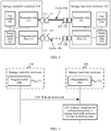
- FIG. 3 is a schematic diagram of structures and a connection manner of a storage controller enclosure and a storage hard disk enclosure that are directly connected in the storage system shown in FIG. 1 in an embodiment of the present invention.
- FIG. 3 shows the storage controller enclosure 210 and the storage hard disk enclosure 220 that are included in the storage system 200, and the present invention is not limited thereto.
- Two storage devices shown in FIG. 3 may be any two directly connected storage devices in the storage system shown in FIG. 1 , for example, the storage controller enclosure 210 and the storage hard disk enclosure 230, or the storage hard disk enclosure 220 and the storage hard disk enclosure 240.
- the storage controller enclosure 210 and the storage hard disk enclosure 220 are merely used as an example for description.
- the storage controller enclosure 210 and the storage hard disk enclosure 220 are connected together in series.
- the storage controller enclosure 210 includes a programmable chip 212, and the programmable chip 212 is configured to perform baseboard management (may also be referred to as board management) for the storage controller enclosure 210.
- the storage hard disk enclosure 220 includes a programmable chip 222, and the programmable chip 222 is configured to perform baseboard management for the storage hard disk enclosure 220.
- the programmable chip 212 of the storage controller enclosure 210 and the programmable chip 222 of the storage hard disk enclosure 220 are connected together in series.
- the storage hard disk enclosure 220 is in a sleep state, and the sleep state means that only the programmable chip 222 is in a power-on state.
- the programmable chip 212 of the storage controller enclosure 210 is configured to send a wakeup instruction to the programmable chip 222 of the storage hard disk enclosure 220.
- the programmable chip 222 of the storage hard disk enclosure 220 is configured to receive the wakeup instruction sent by the programmable chip 212, and controls, based on the wakeup instruction, the storage hard disk enclosure 220 to enter a working state.
- the working state means that all elements of the storage hard disk enclosure 220 are in the power-on state.
- the storage controller enclosure 210 includes an expander chip 211, the programmable chip 212, a power supply chip 213, a fan module 214, and an interface 215 connected to the expander chip 211.
- the storage hard disk enclosure 220 includes an expander chip 221, the programmable chip 222, a power supply chip 223, a fan module 224, and an interface 225 connected to the expander chip 221.
- the programmable chip 212 of the storage controller enclosure 210 and the programmable chip 222 of the storage hard disk enclosure 220 are connected together in series.
- the expander chip 211 and the expander chip 221 are configured to receive and send respective storage-related control information and service data.
- the programmable chip 212 of the storage controller enclosure 210 is configured to implement baseboard management in the storage controller enclosure 210, that is, perform simple management for the units in the storage controller enclosure 210, for example, power-on and power-off management, temperature measurement, and input/output (Input/Output, "I/O" for short) management for the units in the storage controller enclosure 210.
- the programmable chip 222 of the storage controller enclosure 220 is configured to implement baseboard management in the storage hard disk enclosure 220.
- the programmable chip 212 is further configured to send the wakeup instruction and a sleep instruction
- the programmable chip 222 is further configured to receive the wakeup instruction and the sleep instruction to control the storage controller enclosure 220 to enter the working state or the sleep state.
- the programmable chip 222 may power off, by controlling the power supply chip 223, the expander chip 221 and the fan module 224 that are connected to the power supply chip 223, to reduce electricity consumption.
- the programmable chip 222 may control the power supply chip 223 of the storage hard disk enclosure 220 based on the wakeup instruction, to enable all elements connected to the power supply chip 223 to enter the working state.
- a wakeup instruction may be sent and received by directly using programmable chips of two storage devices by connecting the programmable chips of the two storage devices in series. Therefore, when the storage device is in the sleep state, neither an expander chip nor a system fan needs to be switched on, thereby reducing electricity consumption of the storage device in the sleep state.
- the programmable chip 212 of the storage controller enclosure 210 is further configured to: when the storage hard disk enclosure 220 is in the working state, send the sleep instruction to the programmable chip 222 of the storage hard disk enclosure 220; and the programmable chip 222 of the storage hard disk enclosure 220 is further configured to: receive the sleep instruction sent by the programmable chip 212, and control, based on the sleep instruction, the storage hard disk enclosure 220 to enter the sleep state.
- both a process of sending, by the storage controller enclosure 210, the wakeup instruction to the storage hard disk enclosure 220 to enable the storage hard disk enclosure 220 to enter the working state, and a process of sending, by the storage controller enclosure 210, the sleep instruction to the storage hard disk enclosure 220 to enable the storage hard disk enclosure 220 to enter the sleep state may be implemented by using the programmable chip 212 of the storage controller enclosure 210 and the programmable chip 222 of the storage hard disk enclosure 220.
- a process of sending, by the storage controller enclosure 210, the wakeup instruction to the storage hard disk enclosure 220 to enable the storage hard disk enclosure 220 to enter the working state may be implemented by using the programmable chip 212 and the programmable chip 222
- a process of sending, by the storage controller enclosure 210, the sleep instruction to the storage hard disk enclosure 220 to enable the storage hard disk enclosure 220 to enter the sleep state may be implemented by using the expander chip 211 of the storage controller enclosure 210 and the expander chip 221 of the storage hard disk enclosure 220.
- both a process of controlling a storage device to enter the working state and a process of controlling a storage device to enter the sleep state are controlled by using programmable chips of the storage devices. Therefore, complexity of signaling transmission between the storage devices can be reduced.
- An example in which a programmable chip is used to control a storage device to switch between the sleep state and the working state is used for description below.
- the channel may be a communications cable such as an ordinary cable or an optical fiber. Two connection manners of the cable that are provided in this embodiment of the present invention are described below.
- the storage controller enclosure 210 includes the expander chip 211 and the interface 215 that are connected to each other.
- the storage hard disk enclosure 220 includes the expander chip 221 and the interface 225 that are connected to each other.
- the interface 215 and the interface 225 further include free pins.
- a cable 130 connected between the interface 215 and the interface 225 includes a port 131 and a port 132, and the port 131 and the port 132 further include free pins.
- a signal cable used to transmit the wakeup instruction and the sleep instruction is connected between the free pin of the port 131 of the cable 130 and the free pin of the port 132 of the cable 130.
- the signal cable is represented by using a dashed line, and the signal cable is located in the cable 130.
- the free pin of the port 131 is connected to the free pin of the interface 215, the free pin of the port 132 is connected to the free pin of the interface 225, the programmable chip 212 is connected to the free pin of the interface 215, and the programmable chip 222 is connected to the free pin of the interface 225.
- the wakeup instruction or the sleep instruction sent by the programmable chip 212 may be transmitted to the programmable chip 222 by using the signal cable between the free pin of the port 131 and the free pin of the port 132. Therefore, the programmable chip 222 controls the power supply chip 223 connected to the programmable chip 222, to enable only the programmable chip 222 to be in the working state, and the storage hard disk enclosure 220 to enter the sleep state; or powers on all elements connected to the power supply chip 223, to enable the storage hard disk enclosure 220 to enter the working state.
- free pins may be reserved pins at the port 131 and the port 132, or may be newly added pins at the port 131 and the port 132. This is not limited in the present invention.
- the storage controller enclosure 210 includes an interface 216 connected to the programmable chip 112, and the storage hard disk enclosure 220 includes an interface 226 connected to the programmable chip 222.
- a cable 140 connected between the interface 216 and the fourth interface 226 includes a port 141 and a port 142, the port 141 is connected to the interface 216, and the port 142 is connected to the interface 226.
- FIG. 4 shows examples of structures and another connection manner of the storage controller enclosure and the storage hard disk enclosure that are directly connected.
- the new cable 140 may alternatively be directly disposed between the programmable chip 212 and the programmable chip 222.
- the cable 140 includes an independent port 141 and an independent port 142, and the port 141 and the port 142 are respectively connected to the interface 216 and the interface 226, so that the wakeup instruction or the sleep instruction may be transmitted by using the cable 140.
- the transmission is more conveniently implemented by adding the new connection cable 140 between the programmable chips.
- the transmission of the wakeup instruction and the sleep instruction is not affected.
- the cable 130 herein may also be referred to as a high speed signal cable in some cases, and the cable 140 may also be referred to as a low speed signal cable.
- the transmission channel established between the programmable chip 212 and the programmable chip 222 in the foregoing two manners not only may be used to transmit the wakeup instruction and the sleep instruction, but also may be used to transmit another control command, for example, a command used to reset the expander chip.
- a command to be transmitted may be determined based on a requirement. This is not limited either in the present invention.
- the storage system may include at least one storage hard disk enclosure.
- the wakeup instruction may be used to instruct the at least one hard disk enclosure in the storage system to switch from the sleep state to the working state.
- the storage hard disk enclosure 220 may be controlled, by using the programmable chips, to enter the working state.
- the hard disk enclosure 240 may also be controlled, by using programmable chips, to enter the working state. This is not limited in the present invention.
- At least two storage devices in the storage system in FIG. 1 include a storage controller enclosure and at least one hard disk enclosure.
- the server sends a wakeup instruction or a sleep instruction to the first storage device.
- the first storage device After receiving the wakeup instruction, the first storage device sends the wakeup instruction to the second storage device. That is, the wakeup instruction sent by the first storage device to the second storage device is from the server.
- the storage controller enclosure receives a wakeup instruction or a sleep instruction sent by the server, and sends the wakeup instruction or the sleep instruction to the first storage device.
- the first storage device sends the received wakeup instruction or sleep instruction to the second storage device. That is, the wakeup instruction or the sleep instruction sent by the first storage device is from the storage controller enclosure.
- the storage system, and the storage devices and the connection manner of the storage devices in the storage system according to the embodiments of the present invention are described above in detail, and a method for transmitting a signal in a storage system according to an embodiment of the present invention is described below. It should be understood that the method for transmitting a signal in a storage system in this embodiment of the present invention may be performed by storage devices in the foregoing embodiments of the present invention. That is, for the following specific implementations of the method, refer to the foregoing descriptions of the embodiments of the storage device and the system.
- FIG. 5 is a procedure interaction diagram of a method for transmitting a signal in a storage system according to an embodiment of the present invention.
- signal transmission between a storage controller enclosure 210 and a storage hard disk enclosure 220 in the storage system in FIG. 2 is used as an example for description.
- FIG. 5 shows the storage controller enclosure 210 and the storage hard disk enclosure 220.
- the method is also applicable to signal transmission between storage hard disk enclosures that are cascaded with each other in the storage system. For brevity, details are not described herein.
- the storage controller enclosure 210 includes a programmable chip 212, the storage hard disk enclosure 220 includes a programmable chip 222, the storage controller enclosure 210 and the storage hard disk enclosure 220 are connected together in series, the programmable chip 212 is configured to perform baseboard management for the storage controller enclosure 210, the storage hard disk enclosure 220 includes the programmable chip 222, the programmable chip 222 is configured to perform baseboard management for the storage hard disk enclosure 220, the programmable chip 212 of the storage controller enclosure 210 and the programmable chip 222 of the storage hard disk enclosure 220 are connected together in series, the storage hard disk enclosure 220 is in a sleep state, and the sleep state means that only the programmable chip 222 is in a power-on state.
- the method includes the following steps.
- the programmable chip 212 of the storage controller enclosure 210 sends a wakeup instruction to the programmable chip 222 of the storage hard disk enclosure 220.
- the programmable chip 222 of the storage hard disk enclosure 220 receives the wakeup instruction sent by the programmable chip 212 of the storage controller enclosure 210, and controls, based on the wakeup instruction, the storage hard disk enclosure 220 to enter a working state, where the working state means that all elements of the storage hard disk enclosure 220 are in the power-on state.
- a storage device is controlled, by using a programmable chip of the storage device, to switch from the sleep state to the working state, electricity consumption generated by an expander chip and a system fan when the storage device is in the sleep state can be reduced.
- an application server 260 sends the wakeup instruction to the storage controller enclosure 210, and the wakeup instruction is used to instruct the hard disk enclosure in the storage system to enter the working state.
- the storage controller enclosure 210 sends the wakeup instruction to the programmable chip 222 of the storage hard disk enclosure 220 by using the programmable chip 212 of the storage controller enclosure 210.
- the programmable chip 222 controls a power supply module 223 based on the wakeup instruction, so that all the elements of the storage hard disk enclosure 220 are in the power-on state.
- the programmable chip 222 of the storage hard disk enclosure 220 may further send the wakeup instruction to a storage hard disk enclosure serially connected to the storage hard disk enclosure 220, for example, a storage hard disk enclosure 240.
- a programmable chip 242 of the storage hard disk enclosure 240 receives the wakeup instruction sent by the programmable chip 222, and controls, based on the wakeup instruction, the storage hard disk enclosure 240 to enter the working state.
- the programmable chip 242 of the storage hard disk enclosure 240 may further continue to send, in sequence, the wakeup instruction to a storage hard disk enclosure serially connected to the storage hard disk enclosure 240 until all hard disk enclosures in the storage system complete wakeup or sleep operations.
- the method further includes: sending, by the programmable chip 212 of the storage controller enclosure 210, a sleep instruction to the programmable chip 222 of the storage hard disk enclosure 220 when the storage hard disk enclosure 220 is in the working state; and receiving, by the programmable chip 222 of the storage hard disk enclosure 220, the sleep instruction sent by the programmable chip 212, and controlling, based on the sleep instruction, the storage hard disk enclosure 220 to enter the sleep state.
- the storage hard disk enclosure includes an expander chip, a programmable chip, and a system fan.
- Table 1 shows electricity consumption of the storage hard disk enclosure when the storage hard disk enclosure is controlled by the expander chip to enter the working state; and electricity consumption of the storage hard disk enclosure when the storage hard disk enclosure is controlled by the programmable chip to enter the working state.
- sequence numbers of the foregoing processes do not mean execution sequences in the embodiments of the present invention.
- the execution sequences of the processes should be determined based on functions and internal logic of the processes, and should not be construed as any limitation on the implementation processes of the embodiments of the present invention.
- a person of ordinary skill in the art may understand that all or some of the steps in the communication method in the embodiments of the present invention may be implemented by a program instructing relevant hardware.
- the program may be stored in a readable storage medium. When the program is run, the corresponding steps in the communication method are performed.
- the programmable chip may be a field programmable gate array (Field Programmable Gates Array, "FPGA” for short), a baseboard management controller (Baseboard Management Controller, "BMC” for short), a complex programmable logic device (Complex Programmable Logic Device, "CPLD” for short), another programmable logical device, or the like.
- FPGA Field Programmable Gates Array
- BMC Baseboard Management Controller
- CPLD Complex Programmable Logic Device
- CPLD Complex Programmable Logic Device
- the units described as separate parts may or may not be physically separate, and parts displayed as units may or may not be physical units, may be located in one position, or may be distributed on a plurality of network units. Some or all of the units may be selected according to actual needs to achieve the objectives of the solutions of the embodiments of the present invention.
Landscapes
- Engineering & Computer Science (AREA)
- Theoretical Computer Science (AREA)
- General Engineering & Computer Science (AREA)
- Physics & Mathematics (AREA)
- General Physics & Mathematics (AREA)
- Human Computer Interaction (AREA)
- Computer Hardware Design (AREA)
- Computing Systems (AREA)
- Power Sources (AREA)
Claims (7)
- Speichersystem, umfassend mindestens zwei Vorrichtungen (210, 220, 230, 240, 250, 260, 270), wobei die mindestens zwei Vorrichtungen in Reihe miteinander verbunden sind, wobei die mindestens zwei Vorrichtungen eine erste Vorrichtung (210, 220) und eine zweite Vorrichtung (220, 230) umfassen, wobei jede der ersten Vorrichtung und der zweiten Vorrichtung einen programmierbaren Chip (212, 222) und einen Expanderchip (211, 221) umfasst, wobei der programmierbare Chip ausgestaltet ist, ein Baseboardmanagement für die erste Vorrichtung und die zweite Vorrichtung durchzuführen, und der Expanderchip (211, 221) ausgestaltet ist, einen Speicherdienst zu verarbeiten, wobei ein erster programmierbarer Chip (212) der ersten Vorrichtung und ein zweiter programmierbarer Chip (222) der zweiten Vorrichtung durch ein Kommunikationskabel (130, 140) in Reihe miteinander verbunden sind, wobei die zweite Vorrichtung ausgestaltet ist, sich in einem Bereitschaftszustand zu befinden, und wobei der Bereitschaftszustand bedeutet, dass sich nur der zweite programmierbare Chip in einem eingeschalteten Zustand befindet;
wobei der erste programmierbare Chip (212) ausgestaltet ist, eine Aktivierungsanweisung an den zweiten programmierbaren Chip zu senden; und
wobei der zweite programmierbare Chip (222) zu Folgendem ausgestaltet ist: Empfangen der durch den ersten programmierbaren Chip (212) gesendeten Aktivierungsanweisung, und Steuern, basierend auf der Aktivierungsanweisung, der zweiten Vorrichtung, in einen Arbeitszustand einzutreten, wobei der Arbeitszustand bedeutet, dass sich alle Elemente der zweiten Vorrichtung in dem eingeschalteten Zustand befinden. - Speichersystem nach Anspruch 1, wobei die erste Vorrichtung (210) einen ersten Expanderchip (211) und eine erste Schnittstelle (215) umfasst, die miteinander verbunden sind, wobei die zweite Vorrichtung (220) einen zweiten Expanderchip (221) und eine zweite Schnittstelle (225) umfasst, die miteinander verbunden sind, wobei die erste Schnittstelle (215) und die zweite Schnittstelle (225) ferner freie Kontakte umfassen, wobei ein Kabel (130), das zwischen der ersten Schnittstelle (215) und der zweiten Schnittstelle (225) verbunden ist, einen ersten Anschluss (131) und einen zweiten Anschluss (132) umfasst, und wobei der erste Anschluss (131) und der zweite Anschluss (132) ferner freie Kontakte umfassen; und
wobei, wenn der erste Anschluss (131) mit der ersten Schnittstelle (215) verbunden ist, der freie Kontakt des ersten Anschlusses (215) mit dem freien Kontakt der ersten Schnittstelle (215) verbunden ist, und wenn der zweite Anschluss (132) mit der zweiten Schnittstelle (225) verbunden ist, der freie Kontakt des zweiten Anschlusses (225) mit dem freien Kontakt der zweiten Schnittstelle (225) verbunden ist, wobei der erste programmierbare Chip (212) mit dem freien Kontakt der ersten Schnittstelle (215) verbunden ist, und der zweite programmierbare Chip (222) mit dem freien Kontakt der zweiten Schnittstelle (225) verbunden ist. - Speichersystem nach Anspruch 1 oder 2, wobei die mindestens zwei Vorrichtungen eine Speichersteuerung (210) und mindestens einen Universalspeicher (220) umfassen, wobei die erste Vorrichtung (210) die Speichersteuerung (210) ist und die zweite Vorrichtung (220) die direkt mit der Speichersteuerung verbundene Universalspeichervorrichtung ist, und die Aktivierungsanweisung oder eine Bereitschaftsanweisung, die durch die erste Vorrichtung gesendet wird, von einem Server stammt.
- Speichersystem nach einem der Ansprüche 1 bis 3, wobei die mindestens zwei Vorrichtungen eine Speichersteuerung (210) und mindestens zwei Universalspeicher umfassen, wobei die Speichersteuerung ausgestaltet ist, eine Aktivierungsanweisung oder eine Bereitschaftsanweisung zu empfangen, die durch einen Server gesendet wird, und wobei die erste Vorrichtung und die zweite Vorrichtung zwei direkt verbundene Universalspeicher in den mindestens zwei Universalspeichern sind, und die Aktivierungsanweisung oder eine Bereitschaftsanweisung, die durch die erste Vorrichtung gesendet wird, von der Speichersteuerung stammt.
- Speichersystem nach Anspruch 3 oder 4, wobei der erste programmierbare Chip ferner zu Folgendem ausgestaltet ist:Senden der Bereitschaftsanweisung an den zweiten programmierbaren Chip, wobei sich die zweite Vorrichtung in einem Arbeitszustand befindet; undwobei der zweite programmierbare Chip ferner zu Folgendem ausgestaltet ist: Empfangen der durch den ersten programmierbaren Chip gesendeten Bereitschaftsanweisung, und Steuern, basierend auf der Bereitschaftsanweisung, der zweiten Vorrichtung, in einen Bereitschaftszustand einzutreten.
- Verfahren zum Übertragen eines Signals in einem Speichersystem nach Anspruch 1, wobei das Verfahren umfasst:Senden, durch den ersten programmierbaren Chip (212), einer Aktivierungsanweisung an den zweiten programmierbaren Chip; undEmpfangen, durch den zweiten programmierbaren Chip (222), der durch den ersten programmierbaren Chip gesendeten Aktivierungsanweisung, und Steuern, basierend auf der Aktivierungsanweisung, der zweiten Vorrichtung, in einen Arbeitszustand einzutreten, wobei der Arbeitszustand bedeutet, dass sich alle Elemente der zweiten Vorrichtung in einem eingeschalteten Zustand befinden.
- Verfahren nach Anspruch 6, wobei das Verfahren ferner umfasst:Senden, durch den ersten programmierbaren Chip (212), einer Bereitschaftsanweisung an den zweiten programmierbaren Chip, wobei sich die zweite Vorrichtung in dem Arbeitszustand befindet; undEmpfangen, durch den zweiten programmierbaren Chip (222), der durch den ersten programmierbaren Chip gesendeten Bereitschaftsanweisung, und Steuern, basierend auf der Bereitschaftsanweisung, der zweiten Vorrichtung, in den Bereitschaftszustand einzutreten.
Applications Claiming Priority (2)
| Application Number | Priority Date | Filing Date | Title |
|---|---|---|---|
| CN201610785537.2A CN107783726B (zh) | 2016-08-31 | 2016-08-31 | 存储系统和存储系统中传输信号的方法 |
| PCT/CN2017/099448 WO2018041093A1 (zh) | 2016-08-31 | 2017-08-29 | 存储系统和存储系统中传输信号的方法 |
Publications (3)
| Publication Number | Publication Date |
|---|---|
| EP3474145A1 EP3474145A1 (de) | 2019-04-24 |
| EP3474145A4 EP3474145A4 (de) | 2019-06-26 |
| EP3474145B1 true EP3474145B1 (de) | 2020-05-13 |
Family
ID=61300181
Family Applications (1)
| Application Number | Title | Priority Date | Filing Date |
|---|---|---|---|
| EP17845395.7A Active EP3474145B1 (de) | 2016-08-31 | 2017-08-29 | Speichersystem und verfahren zur signalübertragung in einem speichersystem |
Country Status (4)
| Country | Link |
|---|---|
| US (1) | US11460908B2 (de) |
| EP (1) | EP3474145B1 (de) |
| CN (1) | CN107783726B (de) |
| WO (1) | WO2018041093A1 (de) |
Families Citing this family (6)
| Publication number | Priority date | Publication date | Assignee | Title |
|---|---|---|---|---|
| TWI735585B (zh) * | 2017-05-26 | 2021-08-11 | 瑞昱半導體股份有限公司 | 具有網路功能的資料管理電路及基於網路的資料管理方法 |
| CN109488628B (zh) * | 2018-11-07 | 2020-09-15 | 苏州浪潮智能科技有限公司 | 一种用于存储系统散热的风扇控制方法、装置及存储介质 |
| KR102405977B1 (ko) * | 2020-08-11 | 2022-06-03 | 이청종 | 전산망 해킹방지 시스템 및 방법 |
| CN112882985A (zh) * | 2021-01-29 | 2021-06-01 | 杭州万高科技股份有限公司 | 一种数据传输系统、方法、装置及介质 |
| CN115495408B (zh) * | 2022-11-16 | 2023-09-01 | 无锡沐创集成电路设计有限公司 | 数据处理方法、芯片模块、合封芯片及电子设备 |
| CN116156435B (zh) * | 2023-02-21 | 2026-02-17 | 珠海泰芯半导体有限公司 | 接入点的连接方法、装置、存储介质及站点 |
Family Cites Families (13)
| Publication number | Priority date | Publication date | Assignee | Title |
|---|---|---|---|---|
| JP4071419B2 (ja) * | 2000-05-25 | 2008-04-02 | 株式会社日立製作所 | ディスクアレイ装置 |
| US7017037B2 (en) * | 2002-06-27 | 2006-03-21 | Microsoft Corporation | Apparatus and method to decrease boot time and hibernate awaken time of a computer system utilizing disk spin-up-time |
| US7624206B2 (en) * | 2005-09-29 | 2009-11-24 | Emc Corporation | RAID data storage system with SAS expansion |
| JP4919752B2 (ja) * | 2006-09-29 | 2012-04-18 | 株式会社日立製作所 | 記憶制御装置 |
| US8897313B2 (en) * | 2007-01-31 | 2014-11-25 | International Business Machines Corporation | Out-of-band signaling support over standard optical SFP |
| CN100518069C (zh) * | 2007-05-25 | 2009-07-22 | 杭州华三通信技术有限公司 | 电源管理方法、系统及主控板和智能接口板 |
| CN101403945B (zh) * | 2008-11-03 | 2010-10-27 | 成都市华为赛门铁克科技有限公司 | 存储系统及其节能方法 |
| US8756445B2 (en) * | 2010-01-06 | 2014-06-17 | Apple Inc. | Providing power to an accessory during portable computing device hibernation |
| CN201867678U (zh) * | 2010-08-30 | 2011-06-15 | 微星科技股份有限公司 | 在休眠下可降低耗电量的计算机主机板 |
| US8443221B2 (en) * | 2011-03-04 | 2013-05-14 | Sandisk Technologies Inc. | Methods, systems, and computer readable media for advanced power management for serial advanced technology attachment (SATA)-based storage devices |
| GB2506572A (en) * | 2012-07-05 | 2014-04-09 | Ibm | Blade enclosure with control and expansion canisters |
| KR101716885B1 (ko) * | 2013-10-18 | 2017-03-27 | 주식회사 엘지화학 | 입력 커넥터 및 출력 커넥터의 구분 없이 데이지 체인 통신망을 구성할 수 있는 통신단말기 |
| US9939865B2 (en) * | 2014-06-13 | 2018-04-10 | Seagate Technology Llc | Selective storage resource powering for data transfer management |
-
2016
- 2016-08-31 CN CN201610785537.2A patent/CN107783726B/zh active Active
-
2017
- 2017-08-29 WO PCT/CN2017/099448 patent/WO2018041093A1/zh not_active Ceased
- 2017-08-29 EP EP17845395.7A patent/EP3474145B1/de active Active
-
2019
- 2019-02-28 US US16/289,621 patent/US11460908B2/en active Active
Non-Patent Citations (1)
| Title |
|---|
| None * |
Also Published As
| Publication number | Publication date |
|---|---|
| EP3474145A4 (de) | 2019-06-26 |
| CN107783726A (zh) | 2018-03-09 |
| WO2018041093A1 (zh) | 2018-03-08 |
| CN107783726B (zh) | 2019-11-12 |
| EP3474145A1 (de) | 2019-04-24 |
| US11460908B2 (en) | 2022-10-04 |
| US20190196569A1 (en) | 2019-06-27 |
Similar Documents
| Publication | Publication Date | Title |
|---|---|---|
| US11460908B2 (en) | Storage system and method for transmitting signal in storage system | |
| US4663539A (en) | Local power switching control subsystem | |
| US4677566A (en) | Power control network for multiple digital modules | |
| US8015420B2 (en) | System and method for power management of a storage enclosure | |
| US7710718B2 (en) | Method and apparatus for enforcing of power control in a blade center chassis | |
| CN106850286B (zh) | 单板上的基板管理控制器及网元管理盘的基板管理控制器 | |
| EP2863723B1 (de) | Vorrichtungsverwaltungsmodul, Fernverwaltungsmodul und Vorrichtungsverwaltungssystem damit | |
| CN109857614A (zh) | 一种机架服务器的容灾装置和方法 | |
| CN104516478B (zh) | 对设备功率进行节流 | |
| CN106814976A (zh) | 集群存储系统及应用其的数据交互方法 | |
| CN104866448A (zh) | 大规模usb设备的智能管理系统 | |
| CN103309422A (zh) | 电源装置 | |
| US9606560B2 (en) | Computer system, arrangement for remote maintenance and remote maintenance method | |
| CN113778667B (zh) | 服务器节点信息管理系统和方法、可读介质 | |
| CN107395530B (zh) | 一种交换芯片、网络设备和功耗控制方法 | |
| WO2025261305A1 (zh) | 供电设备及供电系统 | |
| CN102478905A (zh) | 数据中心 | |
| CN102546719B (zh) | 一种网络远程控制系统、方法及节点机 | |
| CN106708771B (zh) | 一种网络旁路装置及其处理方法 | |
| CN102694719A (zh) | 微型电信计算架构系统、载板集线器模块及pci-e交换器的端口配置方法 | |
| US20080126635A1 (en) | Blade Server Switch Module | |
| CN102420694A (zh) | 基于数据总线的设备远程唤醒系统 | |
| CN107505991A (zh) | 一种灵活配置的多单元服务器系统及配置方法 | |
| CN112162508A (zh) | 一种机框式设备的上下电控制系统和方法 | |
| CN107608462B (zh) | 服务器系统及储存单元的控制方法 |
Legal Events
| Date | Code | Title | Description |
|---|---|---|---|
| STAA | Information on the status of an ep patent application or granted ep patent |
Free format text: STATUS: THE INTERNATIONAL PUBLICATION HAS BEEN MADE |
|
| PUAI | Public reference made under article 153(3) epc to a published international application that has entered the european phase |
Free format text: ORIGINAL CODE: 0009012 |
|
| STAA | Information on the status of an ep patent application or granted ep patent |
Free format text: STATUS: REQUEST FOR EXAMINATION WAS MADE |
|
| 17P | Request for examination filed |
Effective date: 20190117 |
|
| AK | Designated contracting states |
Kind code of ref document: A1 Designated state(s): AL AT BE BG CH CY CZ DE DK EE ES FI FR GB GR HR HU IE IS IT LI LT LU LV MC MK MT NL NO PL PT RO RS SE SI SK SM TR |
|
| AX | Request for extension of the european patent |
Extension state: BA ME |
|
| A4 | Supplementary search report drawn up and despatched |
Effective date: 20190524 |
|
| RIC1 | Information provided on ipc code assigned before grant |
Ipc: G06F 13/42 20060101ALI20190520BHEP Ipc: G06F 3/06 20060101ALI20190520BHEP Ipc: G06F 1/3234 20190101AFI20190520BHEP |
|
| DAV | Request for validation of the european patent (deleted) | ||
| DAX | Request for extension of the european patent (deleted) | ||
| REG | Reference to a national code |
Ref country code: DE Ref legal event code: R079 Ref document number: 602017016881 Country of ref document: DE Free format text: PREVIOUS MAIN CLASS: G06F0012000000 Ipc: G06F0001323400 |
|
| GRAP | Despatch of communication of intention to grant a patent |
Free format text: ORIGINAL CODE: EPIDOSNIGR1 |
|
| STAA | Information on the status of an ep patent application or granted ep patent |
Free format text: STATUS: GRANT OF PATENT IS INTENDED |
|
| RIC1 | Information provided on ipc code assigned before grant |
Ipc: G06F 13/42 20060101ALI20200115BHEP Ipc: G06F 3/06 20060101ALI20200115BHEP Ipc: G06F 1/3234 20190101AFI20200115BHEP |
|
| INTG | Intention to grant announced |
Effective date: 20200206 |
|
| GRAS | Grant fee paid |
Free format text: ORIGINAL CODE: EPIDOSNIGR3 |
|
| GRAA | (expected) grant |
Free format text: ORIGINAL CODE: 0009210 |
|
| STAA | Information on the status of an ep patent application or granted ep patent |
Free format text: STATUS: THE PATENT HAS BEEN GRANTED |
|
| AK | Designated contracting states |
Kind code of ref document: B1 Designated state(s): AL AT BE BG CH CY CZ DE DK EE ES FI FR GB GR HR HU IE IS IT LI LT LU LV MC MK MT NL NO PL PT RO RS SE SI SK SM TR |
|
| REG | Reference to a national code |
Ref country code: GB Ref legal event code: FG4D |
|
| REG | Reference to a national code |
Ref country code: CH Ref legal event code: EP |
|
| REG | Reference to a national code |
Ref country code: DE Ref legal event code: R096 Ref document number: 602017016881 Country of ref document: DE |
|
| REG | Reference to a national code |
Ref country code: AT Ref legal event code: REF Ref document number: 1271118 Country of ref document: AT Kind code of ref document: T Effective date: 20200615 |
|
| REG | Reference to a national code |
Ref country code: LT Ref legal event code: MG4D |
|
| REG | Reference to a national code |
Ref country code: NL Ref legal event code: MP Effective date: 20200513 |
|
| PG25 | Lapsed in a contracting state [announced via postgrant information from national office to epo] |
Ref country code: LT Free format text: LAPSE BECAUSE OF FAILURE TO SUBMIT A TRANSLATION OF THE DESCRIPTION OR TO PAY THE FEE WITHIN THE PRESCRIBED TIME-LIMIT Effective date: 20200513 Ref country code: PT Free format text: LAPSE BECAUSE OF FAILURE TO SUBMIT A TRANSLATION OF THE DESCRIPTION OR TO PAY THE FEE WITHIN THE PRESCRIBED TIME-LIMIT Effective date: 20200914 Ref country code: GR Free format text: LAPSE BECAUSE OF FAILURE TO SUBMIT A TRANSLATION OF THE DESCRIPTION OR TO PAY THE FEE WITHIN THE PRESCRIBED TIME-LIMIT Effective date: 20200814 Ref country code: NO Free format text: LAPSE BECAUSE OF FAILURE TO SUBMIT A TRANSLATION OF THE DESCRIPTION OR TO PAY THE FEE WITHIN THE PRESCRIBED TIME-LIMIT Effective date: 20200813 Ref country code: FI Free format text: LAPSE BECAUSE OF FAILURE TO SUBMIT A TRANSLATION OF THE DESCRIPTION OR TO PAY THE FEE WITHIN THE PRESCRIBED TIME-LIMIT Effective date: 20200513 Ref country code: IS Free format text: LAPSE BECAUSE OF FAILURE TO SUBMIT A TRANSLATION OF THE DESCRIPTION OR TO PAY THE FEE WITHIN THE PRESCRIBED TIME-LIMIT Effective date: 20200913 Ref country code: SE Free format text: LAPSE BECAUSE OF FAILURE TO SUBMIT A TRANSLATION OF THE DESCRIPTION OR TO PAY THE FEE WITHIN THE PRESCRIBED TIME-LIMIT Effective date: 20200513 |
|
| PG25 | Lapsed in a contracting state [announced via postgrant information from national office to epo] |
Ref country code: RS Free format text: LAPSE BECAUSE OF FAILURE TO SUBMIT A TRANSLATION OF THE DESCRIPTION OR TO PAY THE FEE WITHIN THE PRESCRIBED TIME-LIMIT Effective date: 20200513 Ref country code: HR Free format text: LAPSE BECAUSE OF FAILURE TO SUBMIT A TRANSLATION OF THE DESCRIPTION OR TO PAY THE FEE WITHIN THE PRESCRIBED TIME-LIMIT Effective date: 20200513 Ref country code: BG Free format text: LAPSE BECAUSE OF FAILURE TO SUBMIT A TRANSLATION OF THE DESCRIPTION OR TO PAY THE FEE WITHIN THE PRESCRIBED TIME-LIMIT Effective date: 20200813 Ref country code: LV Free format text: LAPSE BECAUSE OF FAILURE TO SUBMIT A TRANSLATION OF THE DESCRIPTION OR TO PAY THE FEE WITHIN THE PRESCRIBED TIME-LIMIT Effective date: 20200513 |
|
| REG | Reference to a national code |
Ref country code: AT Ref legal event code: MK05 Ref document number: 1271118 Country of ref document: AT Kind code of ref document: T Effective date: 20200513 |
|
| PG25 | Lapsed in a contracting state [announced via postgrant information from national office to epo] |
Ref country code: AL Free format text: LAPSE BECAUSE OF FAILURE TO SUBMIT A TRANSLATION OF THE DESCRIPTION OR TO PAY THE FEE WITHIN THE PRESCRIBED TIME-LIMIT Effective date: 20200513 Ref country code: NL Free format text: LAPSE BECAUSE OF FAILURE TO SUBMIT A TRANSLATION OF THE DESCRIPTION OR TO PAY THE FEE WITHIN THE PRESCRIBED TIME-LIMIT Effective date: 20200513 |
|
| PG25 | Lapsed in a contracting state [announced via postgrant information from national office to epo] |
Ref country code: CZ Free format text: LAPSE BECAUSE OF FAILURE TO SUBMIT A TRANSLATION OF THE DESCRIPTION OR TO PAY THE FEE WITHIN THE PRESCRIBED TIME-LIMIT Effective date: 20200513 Ref country code: IT Free format text: LAPSE BECAUSE OF FAILURE TO SUBMIT A TRANSLATION OF THE DESCRIPTION OR TO PAY THE FEE WITHIN THE PRESCRIBED TIME-LIMIT Effective date: 20200513 Ref country code: ES Free format text: LAPSE BECAUSE OF FAILURE TO SUBMIT A TRANSLATION OF THE DESCRIPTION OR TO PAY THE FEE WITHIN THE PRESCRIBED TIME-LIMIT Effective date: 20200513 Ref country code: RO Free format text: LAPSE BECAUSE OF FAILURE TO SUBMIT A TRANSLATION OF THE DESCRIPTION OR TO PAY THE FEE WITHIN THE PRESCRIBED TIME-LIMIT Effective date: 20200513 Ref country code: DK Free format text: LAPSE BECAUSE OF FAILURE TO SUBMIT A TRANSLATION OF THE DESCRIPTION OR TO PAY THE FEE WITHIN THE PRESCRIBED TIME-LIMIT Effective date: 20200513 Ref country code: AT Free format text: LAPSE BECAUSE OF FAILURE TO SUBMIT A TRANSLATION OF THE DESCRIPTION OR TO PAY THE FEE WITHIN THE PRESCRIBED TIME-LIMIT Effective date: 20200513 Ref country code: EE Free format text: LAPSE BECAUSE OF FAILURE TO SUBMIT A TRANSLATION OF THE DESCRIPTION OR TO PAY THE FEE WITHIN THE PRESCRIBED TIME-LIMIT Effective date: 20200513 Ref country code: SM Free format text: LAPSE BECAUSE OF FAILURE TO SUBMIT A TRANSLATION OF THE DESCRIPTION OR TO PAY THE FEE WITHIN THE PRESCRIBED TIME-LIMIT Effective date: 20200513 |
|
| REG | Reference to a national code |
Ref country code: DE Ref legal event code: R097 Ref document number: 602017016881 Country of ref document: DE |
|
| PG25 | Lapsed in a contracting state [announced via postgrant information from national office to epo] |
Ref country code: SK Free format text: LAPSE BECAUSE OF FAILURE TO SUBMIT A TRANSLATION OF THE DESCRIPTION OR TO PAY THE FEE WITHIN THE PRESCRIBED TIME-LIMIT Effective date: 20200513 Ref country code: PL Free format text: LAPSE BECAUSE OF FAILURE TO SUBMIT A TRANSLATION OF THE DESCRIPTION OR TO PAY THE FEE WITHIN THE PRESCRIBED TIME-LIMIT Effective date: 20200513 |
|
| PLBE | No opposition filed within time limit |
Free format text: ORIGINAL CODE: 0009261 |
|
| STAA | Information on the status of an ep patent application or granted ep patent |
Free format text: STATUS: NO OPPOSITION FILED WITHIN TIME LIMIT |
|
| PG25 | Lapsed in a contracting state [announced via postgrant information from national office to epo] |
Ref country code: MC Free format text: LAPSE BECAUSE OF FAILURE TO SUBMIT A TRANSLATION OF THE DESCRIPTION OR TO PAY THE FEE WITHIN THE PRESCRIBED TIME-LIMIT Effective date: 20200513 |
|
| REG | Reference to a national code |
Ref country code: CH Ref legal event code: PL |
|
| 26N | No opposition filed |
Effective date: 20210216 |
|
| PG25 | Lapsed in a contracting state [announced via postgrant information from national office to epo] |
Ref country code: LI Free format text: LAPSE BECAUSE OF NON-PAYMENT OF DUE FEES Effective date: 20200831 Ref country code: LU Free format text: LAPSE BECAUSE OF NON-PAYMENT OF DUE FEES Effective date: 20200829 Ref country code: CH Free format text: LAPSE BECAUSE OF NON-PAYMENT OF DUE FEES Effective date: 20200831 |
|
| REG | Reference to a national code |
Ref country code: BE Ref legal event code: MM Effective date: 20200831 |
|
| PG25 | Lapsed in a contracting state [announced via postgrant information from national office to epo] |
Ref country code: SI Free format text: LAPSE BECAUSE OF FAILURE TO SUBMIT A TRANSLATION OF THE DESCRIPTION OR TO PAY THE FEE WITHIN THE PRESCRIBED TIME-LIMIT Effective date: 20200513 |
|
| PG25 | Lapsed in a contracting state [announced via postgrant information from national office to epo] |
Ref country code: BE Free format text: LAPSE BECAUSE OF NON-PAYMENT OF DUE FEES Effective date: 20200831 Ref country code: IE Free format text: LAPSE BECAUSE OF NON-PAYMENT OF DUE FEES Effective date: 20200829 |
|
| PG25 | Lapsed in a contracting state [announced via postgrant information from national office to epo] |
Ref country code: TR Free format text: LAPSE BECAUSE OF FAILURE TO SUBMIT A TRANSLATION OF THE DESCRIPTION OR TO PAY THE FEE WITHIN THE PRESCRIBED TIME-LIMIT Effective date: 20200513 Ref country code: MT Free format text: LAPSE BECAUSE OF FAILURE TO SUBMIT A TRANSLATION OF THE DESCRIPTION OR TO PAY THE FEE WITHIN THE PRESCRIBED TIME-LIMIT Effective date: 20200513 Ref country code: CY Free format text: LAPSE BECAUSE OF FAILURE TO SUBMIT A TRANSLATION OF THE DESCRIPTION OR TO PAY THE FEE WITHIN THE PRESCRIBED TIME-LIMIT Effective date: 20200513 |
|
| PG25 | Lapsed in a contracting state [announced via postgrant information from national office to epo] |
Ref country code: MK Free format text: LAPSE BECAUSE OF FAILURE TO SUBMIT A TRANSLATION OF THE DESCRIPTION OR TO PAY THE FEE WITHIN THE PRESCRIBED TIME-LIMIT Effective date: 20200513 |
|
| PGFP | Annual fee paid to national office [announced via postgrant information from national office to epo] |
Ref country code: DE Payment date: 20250702 Year of fee payment: 9 |
|
| PGFP | Annual fee paid to national office [announced via postgrant information from national office to epo] |
Ref country code: GB Payment date: 20250703 Year of fee payment: 9 |
|
| PGFP | Annual fee paid to national office [announced via postgrant information from national office to epo] |
Ref country code: FR Payment date: 20250703 Year of fee payment: 9 |