EP3471214A2 - Einpresskontaktstift, leiterplatte, verfahren zum bestücken der leiterplatte und vorrichtung zum bestücken der leiterplatte - Google Patents
Einpresskontaktstift, leiterplatte, verfahren zum bestücken der leiterplatte und vorrichtung zum bestücken der leiterplatte Download PDFInfo
- Publication number
- EP3471214A2 EP3471214A2 EP18199642.2A EP18199642A EP3471214A2 EP 3471214 A2 EP3471214 A2 EP 3471214A2 EP 18199642 A EP18199642 A EP 18199642A EP 3471214 A2 EP3471214 A2 EP 3471214A2
- Authority
- EP
- European Patent Office
- Prior art keywords
- press
- circuit board
- printed circuit
- section
- contact pins
- Prior art date
- Legal status (The legal status is an assumption and is not a legal conclusion. Google has not performed a legal analysis and makes no representation as to the accuracy of the status listed.)
- Granted
Links
Images

Classifications
-
- H—ELECTRICITY
- H01—ELECTRIC ELEMENTS
- H01R—ELECTRICALLY-CONDUCTIVE CONNECTIONS; STRUCTURAL ASSOCIATIONS OF A PLURALITY OF MUTUALLY-INSULATED ELECTRICAL CONNECTING ELEMENTS; COUPLING DEVICES; CURRENT COLLECTORS
- H01R12/00—Structural associations of a plurality of mutually-insulated electrical connecting elements, specially adapted for printed circuits, e.g. printed circuit boards [PCB], flat or ribbon cables, or like generally planar structures, e.g. terminal strips, terminal blocks; Coupling devices specially adapted for printed circuits, flat or ribbon cables, or like generally planar structures; Terminals specially adapted for contact with, or insertion into, printed circuits, flat or ribbon cables, or like generally planar structures
- H01R12/50—Fixed connections
- H01R12/51—Fixed connections for rigid printed circuits or like structures
- H01R12/55—Fixed connections for rigid printed circuits or like structures characterised by the terminals
- H01R12/58—Fixed connections for rigid printed circuits or like structures characterised by the terminals terminals for insertion into holes
- H01R12/585—Terminals having a press fit or a compliant portion and a shank passing through a hole in the printed circuit board
-
- H—ELECTRICITY
- H05—ELECTRIC TECHNIQUES NOT OTHERWISE PROVIDED FOR
- H05K—PRINTED CIRCUITS; CASINGS OR CONSTRUCTIONAL DETAILS OF ELECTRIC APPARATUS; MANUFACTURE OF ASSEMBLAGES OF ELECTRICAL COMPONENTS
- H05K1/00—Printed circuits
- H05K1/02—Details
- H05K1/11—Printed elements for providing electric connections to or between printed circuits
- H05K1/115—Via connections; Lands around holes or via connections
-
- H—ELECTRICITY
- H05—ELECTRIC TECHNIQUES NOT OTHERWISE PROVIDED FOR
- H05K—PRINTED CIRCUITS; CASINGS OR CONSTRUCTIONAL DETAILS OF ELECTRIC APPARATUS; MANUFACTURE OF ASSEMBLAGES OF ELECTRICAL COMPONENTS
- H05K2201/00—Indexing scheme relating to printed circuits covered by H05K1/00
- H05K2201/10—Details of components or other objects attached to or integrated in a printed circuit board
- H05K2201/10227—Other objects, e.g. metallic pieces
- H05K2201/10295—Metallic connector elements partly mounted in a hole of the PCB
- H05K2201/10303—Pin-in-hole mounted pins
-
- H—ELECTRICITY
- H05—ELECTRIC TECHNIQUES NOT OTHERWISE PROVIDED FOR
- H05K—PRINTED CIRCUITS; CASINGS OR CONSTRUCTIONAL DETAILS OF ELECTRIC APPARATUS; MANUFACTURE OF ASSEMBLAGES OF ELECTRICAL COMPONENTS
- H05K2201/00—Indexing scheme relating to printed circuits covered by H05K1/00
- H05K2201/10—Details of components or other objects attached to or integrated in a printed circuit board
- H05K2201/10613—Details of electrical connections of non-printed components, e.g. special leads
- H05K2201/10742—Details of leads
- H05K2201/1075—Shape details
- H05K2201/1081—Special cross-section of a lead; Different cross-sections of different leads; Matching cross-section, e.g. matched to a land
-
- H—ELECTRICITY
- H05—ELECTRIC TECHNIQUES NOT OTHERWISE PROVIDED FOR
- H05K—PRINTED CIRCUITS; CASINGS OR CONSTRUCTIONAL DETAILS OF ELECTRIC APPARATUS; MANUFACTURE OF ASSEMBLAGES OF ELECTRICAL COMPONENTS
- H05K2201/00—Indexing scheme relating to printed circuits covered by H05K1/00
- H05K2201/10—Details of components or other objects attached to or integrated in a printed circuit board
- H05K2201/10613—Details of electrical connections of non-printed components, e.g. special leads
- H05K2201/10742—Details of leads
- H05K2201/1075—Shape details
- H05K2201/10848—Thinned leads
Definitions
- the invention relates to a press-fit contact pin according to the preamble of claim 1.
- Secondary claims relate to the respective preamble, a circuit board, a method for loading the circuit board and a device for loading the circuit board.
- Press-fit contact pins are generally known for providing a mechanical and electrical contact with a plug-in connector in a printed circuit board.
- the press-in contact pin comprises a distal press-in section for insertion into a through-hole corresponding to the press-in section.
- the object underlying the invention is achieved by a press-fit contact pin according to claim 1, a printed circuit board, a method for equipping the printed circuit board and by a device for equipping the printed circuit board.
- a proximal press-in section is provided for pressing into a second through-connection of the printed circuit board.
- the proximal press-fit portion has a transverse extension which is greater than a first transverse extension of the distal press-fit portion.
- multiple heights of a projection of press-fit contact pins of a printed circuit board can thus be realized with a single press-contact pin type.
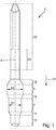
- FIG. 1 shows in a side view of a press-in contact pin 2.
- the press-in contact pins 2 comprises a distal press-in section 4 with a first transverse dimension D1.
- the transverse dimension D1 is measured in a perpendicular plane of the longitudinal axis 6 of the press-fit contact pin 2.
- the press-in contact pin 2 comprises a proximal press-in section 8.
- the proximal press-in section 8 has a second transverse extent D2, which is greater than the first transverse extent D1.
- transverse dimensions D1 and D2 are not readily apparent as suggested, but this only means that the first transverse dimension D1 is rotated, for example, relative to the second transverse extent D2 about the longitudinal axis.
- the transverse dimensions D1 and D2 are thus a respective maximum transverse extent in the region of the press-in sections 4 and 8.
- an inlet section 14 for the first distal press-in section 4 adjoins a distal insertion section 12.
- the cross-section of the insertion section 14 decreases.
- an inlet section 16 is provided, which separates the two press-in sections 4 and 8 from one another.
- an outlet section 18 adjoins the proximal press-in section 8.
- An engaging portion 20 is provided for holding the EinpressWalletlixs means of a gripping device for a press-fit.
- a contact section 22 is arranged for the mechanical and electrical contacting of a mating plug-in region of a mating connector.
- the press-in contact pin 2 is made, for example, from a tinned copper alloy.
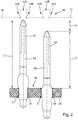
- FIG. 2 shows a schematic sectional view of the circuit board 23, in which the first press-in contact pin 2A is pressed with its distal press-in section 4 in a first through-hole 24.
- the second press-in contact pin 2B is pressed with its proximal press-in section 8 in a second through-connection 28.
- the plated-through holes 24 and 28 are adapted with their inner diameter to the respective provided press-in region 4, 8.
- the vias 24 and 28 are disposed in a respective bore of the circuit board 23 and include, for example, tinned copper alloy.
- the distal end of the contact region 22 of the first press-in contact pin 2A protrudes by a length L1 from one Surface 30 of the circuit board 23 from.
- the distal end of the contact region 22 of the second press-in contact pin 2B protrudes from the surface 30 of the printed circuit board 23 by a length L2 reduced compared to the length L1.
- the first press-fit contact pin 2A protrudes by a press-in difference ⁇ L with respect to the second press-in contact pin 2B.
- the insertion difference ⁇ L is greater than the thickness of the printed circuit board 23.
- the Einpressunter Kunststoff .DELTA.L is selected from 1.8 mm, wherein the inlet portion 16, the two press-in sections 4 and 8 by about 0.2 mm from each other spaced.
- a mating connector 40 is schematically shown, which has corresponding to the contact portions 22 of the Einpressromechanenchanenchane 2A and 2B mating contact portions 42A and 42B.
- the mating contact portions 42A and 42B are formed substantially hollow cylindrical and represent two respectively opposite contact elements 44A and 44B and 44C and 44D for receiving and for mechanical and electrical contacting of the respective contact portion 22 of the Einpressessorstatte 2A and 2B.
- the contact elements 44A-D in a level 41 lying contact points for the Einpressessorstatte 2A and 2B ready.
- the first press-in contact pin 2A leads as a single press-contact pin against a number of second press-in contact pins 2B.
- the first Einpressness 2A is provided for the preparation of a ground contact and connected according to the circuit board 23 for grounding. Advancing the press-fit contact pin 2A damages the control devices by pre-contacting a non-ground connection Prevented, since first of all the electrical contacting of the ground terminal via the press-in contact pin 2A takes place.
- the second press-in contact pin 2B lags behind a number of first press-in contact pins 2A as the only press-fit contact pin.
- the second press-in contact pin 2B is provided to detect a secure contacting of the number of first EinpressANDstatte 2A, for example by means of a verification device on the circuit board 23. If a measurable current flows via the trailing second press-in contact pin 2B, it can be assumed that contacting of the number of first press-in contact pins 2A is present.
- FIG. 3 shows a device 50 for mounting the circuit board 23 with the EinpressANDstatten 2A and 2B in a schematic form.
- the circuit board 23 On a schematically illustrated frame 52, the circuit board 23 is located. Gripping devices 54A and 54B are supported on the frame 52.
- the gripping devices 54A, 54B engage the respective engaging portion 20 of the respective press-fit contact pins 2A and 2B and press the respective press-in contact pins 2A and 2B into the press-fit direction 10 and thus into the corresponding through-holes 24, 28. It is the respective end positions of the gripping devices 54A and 54B shown.
- the device 50 provides different press-in depths for the press-fit contact pins 2A and 2B to be arranged.
- the device 50 may, for example, be divided into two placement stations, wherein the first placement station reaches the first end position of the gripping device 54A and the second placement station reaches a second end position of the gripping device 54B.
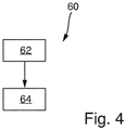
- FIG. 4 2 shows a schematic flow diagram 60 for equipping the printed circuit board 23 with a number of press-fit contact pins 2.
- a distal press-in section 4 of a first of the press-in contact pins 2 is pressed into the first through-connection 24 of the printed circuit board 23, wherein the distal press-in section 4 has a first transverse extension D2 having.
- the proximal press-in section 8 of a second of the press-fit contact pins 2 is pressed into the second through-connection 28 of the printed circuit board 23.
- steps 62 and 64 may also be performed in reverse order.
Landscapes
- Engineering & Computer Science (AREA)
- Microelectronics & Electronic Packaging (AREA)
- Coupling Device And Connection With Printed Circuit (AREA)
- Multi-Conductor Connections (AREA)
Abstract
Description
- Die Erfindung betrifft einen Einpresskontaktstift nach dem Oberbegriff des Anspruchs 1. Nebengeordneten Ansprüche betreffen nach dem jeweiligen Oberbegriff eine Leiterplatte, ein Verfahren zum Bestücken der Leiterplatte und eine Vorrichtung zum Bestücken der Leiterplatte.
- Einpresskontaktstifte sind allgemein bekannt, um, in Durchkontaktierung in einer Leiterplatte angeordnet, eine mechanische und elektrische Kontaktierung mit einem Steckverbinder bereitzustellen. Hierzu umfasst der Einpresskontaktstift einen distalen Einpressabschnitt zur Einpressung in eine dem Einpressabschnitt entsprechende Durchkontaktierung.
- Damit Einpresskontaktstifte in verschiedenen Höhen von der Leiterplatte abstehen, müssen unterschiedlich lang gestaltete Einpresskontaktstifte vorgehalten werden. Hierdurch entstehen höhere Kosten.
- Mithin ist es Aufgabe der Erfindung, einen Einpresskontaktstift bereitzustellen, der die Fertigungskosten senkt.
- Die der Erfindung zugrunde liegende Aufgabe wird durch einen Einpresskontaktstift nach dem Anspruch 1, eine Leiterplatte, ein Verfahren zum Bestücken der Leiterplatte sowie durch eine Vorrichtung zum Bestücken der Leiterplatte gelöst. Vorteilhafte Weiterbildungen sind in den Unteransprüchen und in der nachfolgenden Beschreibung angegeben.
- Erfindungsgemäß ist ein proximaler Einpressabschnitt zur Einpressung in eine zweite Durchkontaktierung der Leiterplatte vorgesehen. Der proximale Einpressabschnitt weist eine Querausdehnung auf, welche größer ist als eine erste Querausdehnung des distalen Einpressabschnitts.
- Vorteilhaft können so mit einem einzigen Einpresskontaktstift-Typ mehrere Höhen einer Abragung von Einpresskontaktstiften von einer Leiterplatte realisiert werden. Durch unterschiedliche Höhen der Abragung können werden bestimmte Funktionen realisiert, beispielsweise eine Erstkontaktierung der Masse beim Aufstecken eines Steckverbinders oder eine Überprüfung der Kontaktierung der Einpresskontaktstifte. Mithin wird unter Reduktion der Fertigungskosten eine Integration weiterer Steckfunktionen ermöglicht.
- In der nachfolgenden Zeichnung werden auch bei unterschiedlichen Ausführungsformen die Merkmale teilweise die gleichen Bezugszeichen verwendet, ohne dass hierauf nochmals explizit hingewiesen wird. In der Zeichnung zeigen:
- Figur 1
- in einer Seitenansicht einen Einpresskontaktstift;
- Figur 2
- in schematischer Schnittansicht eine Leiterplatte mit Einpresskontaktstiften;
- Figur 3
- eine Vorrichtung zum Bestücken der Leiterplatte 2B in schematischer Form; und
- Figur 4
- ein schematisches Ablaufdiagramm.
-
Figur 1 zeigt in einer Seitenansicht einen Einpresskontaktstift 2. Der Einpresskontaktstifte 2 umfasst einen distalen Einpressabschnitt 4 mit einer ersten Querausdehnung D1. Die Querausdehnung D1 bemisst sich in einer Lotebene der Längsachse 6 des Einpresskontaktstifts 2. In proximaler Richtung umfasst der Einpresskontaktstift 2 einen proximalen Einpressabschnitt 8. Der proximale Einpressabschnitt 8 weist eine zweite Querausdehnung D2 auf, welche größer ist als die erste Querausdehnung D1. Selbstverständlich sind Ausführungsformen denkbar, bei denen in einer Seitenansicht die Querausdehnungen D1 und D2 nicht wie vorgeschlagen ohne Weiteres ersichtlich sind, was aber lediglich bedeutet, dass die erste Querausdehnung D1 beispielsweise gegenüber der zweiten Querausdehnung D2 um die Längsachse verdreht ist. Bei den Querausdehnungen D1 und D2 handelt es sich somit eine jeweilige maximale Querausdehnung im Bereich der Einpressabschnitt 4 und 8. - Entgegen einer Einpressrichtung 10 schließt sich an einen distalen Einführabschnitt 12 ein Einlaufabschnitt 14 für den ersten distalen Einpressabschnitt 4 an. In Einpressrichtung 10 nimmt der Querschnitt des Einführabschnitts 14 ab. Zwischen dem distalen Einpressabschnitt 4 und dem proximalen Einpressabschnitt 8 ist ein Einlaufabschnitt 16 vorgesehen, der die beiden Einpressabschnitte 4 und 8 voneinander beabstandet. In proximaler Richtung schließt sich an den proximalen Einpressabschnitt 8 ein Auslaufabschnitt 18 an. Ein Angriffabschnitt 20 ist zur Halterung des Einpresskontaktstifts mittels einer Greifvorrichtung zu einer Einpressung vorgesehen. Entgegen der Einpressrichtung 10 ist ein Kontaktabschnitt 22 zur mechanischen und elektrischen Kontaktierung eines Gegensteckbereichs eines Gegensteckverbinders angeordnet. Der Einpresskontaktstift 2 ist beispielsweise aus einer verzinnten Kupferlegierung gefertigt.
-
Figur 2 zeigt in schematischer Schnittansicht die Leiterplatte 23, in welcher der erste Einpresskontaktstift 2A mit seinem distalen Einpressabschnitt 4 in einer ersten Durchkontaktierung 24 eingepresst ist. Der zweite Einpresskontaktstift 2B ist mit seinem proximalen Einpressabschnitt 8 in einer zweiten Durchkontaktierung 28 eingepresst. Die Durchkontaktierungen 24 und 28 sind mit ihrem Innendurchmesser an den jeweiligen vorgesehenen Einpressbereich 4, 8 angepasst. Die Durchkontaktierungen 24 und 28 sind in einer jeweiligen Bohrung der Leiterplatte 23 angeordnet und umfassen beispielsweise verzinnte Kupferlegierung. - Das distale Ende des Kontaktbereichs 22 des ersten Einpresskontaktstifts 2A ragt um eine Länge L1 von einer Oberfläche 30 der Leiterplatte 23 ab. Das distale Ende des Kontaktbereichs 22 des zweiten Einpresskontaktstifts 2B ragt um eine gegenüber der Länge L1 verringerten Länge L2 von der Oberfläche 30 der Leiterplatte 23 ab. Damit ragt der erste Einpresskontaktstift 2A um einen Einpressunterschied ΔL gegenüber dem zweiten Einpresskontaktstift 2B vor. Der Einpressunterschied ΔL ist größer als die Dicke der Leiterplatte 23. Eine beispielhafte Leiterplattendicke von 1,6 mm vorausgesetzt, wird der Einpressunterschied ΔL von 1,8 mm gewählt, wobei der Einlaufabschnitt 16 die beiden Einpressabschnitte 4 und 8 um etwa 0,2 mm voneinander beabstandet.
- Des Weiteren ist schematisch ein Gegensteckverbinder 40 gezeigt, welcher zu den Kontaktabschnitten 22 der Einpresskontaktstifte 2A und 2B korrespondierende Gegenkontaktabschnitte 42A und 42B aufweist. Die Gegenkontaktabschnitte 42A und 42B sind im Wesentlichen hohlzylindrisch ausgebildet und stellen zwei sich jeweils gegenüberliegende Kontaktelemente 44A und 44B sowie 44C und 44D zur Aufnahme und zur mechanischen und elektrischen Kontaktierung des jeweiligen Kontaktabschnitts 22 der Einpresskontaktstifte 2A und 2B dar. Die Kontaktelemente 44A-D stellen in einer Ebene 41 liegende Kontaktpunkte für die Einpresskontaktstifte 2A und 2B bereit.
- In einer ersten Ausführungsform eilt der erste Einpresskontaktstift 2A als einziger Einpresskontaktstift gegenüber einer Anzahl zweiter Einpresskontaktstifte 2B vor. Der erste Einpresskontaktstift 2A ist zur Herstellung eines Massekontakts vorgesehen und entsprechend auf der Leiterplatte 23 zur Masseeinleitung verschaltet. Durch das Voreilen des Einpresskontaktstifts 2A wird Schäden an Steuergeräten durch Vorkontaktierung eines Nicht-Masseanschlusses vorgebeugt, da zuallererst die elektrische Kontaktierung des Masseanschlusses über den Einpresskontaktstift 2A erfolgt.
- In einer zweiten Ausführungsform eilt der zweite Einpresskontaktstift 2B als einziger Einpresskontaktstift gegenüber einer Anzahl von ersten Einpresskontaktstiften 2A nach. Der zweite Einpresskontaktstift 2B ist dazu vorgesehen, um eine sichere Kontaktierung der Anzahl der ersten Einpresskontaktstifte 2A beispielsweise mithilfe einer Überprüfungseinrichtung auf der Leiterplatte 23 festzustellen. Fließt ein messbarer Strom über den nacheilenden zweiten Einpresskontaktstift 2B, so kann davon ausgegangen werden, dass eine Kontaktierung der Anzahl von ersten Einpresskontaktstiften 2A vorliegt.
-
Figur 3 zeigt eine Vorrichtung 50 zum Bestücken der Leiterplatte 23 mit den Einpresskontaktstiften 2A und 2B in schematischer Form. An einem schematisch dargestellten Rahmen 52 liegt die Leiterplatte 23 an. An dem Rahmen 52 stützen sich Greifvorrichtungen 54A und 54B ab. Die Greifvorrichtungen 54A, 54B greifen an dem jeweiligen Angriffabschnitt 20 des jeweiligen Einpresskontaktstifts 2A und 2B an und drücken den jeweiligen Einpresskontaktstift 2A und 2B in die Einpressrichtung 10 und damit in die zugehörigen Durchkontaktierungen 24, 28. Es sind die jeweiligen Endlagen der Greifvorrichtungen 54A und 54B gezeigt. So stellt die Vorrichtung 50 unterschiedliche Einpresstiefen für die anzuordnenden Einpresskontaktstifte 2A und 2B bereit. Vorteilhaft entfällt durch eine derartige Vorrichtung 50 ein Werkzeugwechsel und es müssen nicht zusätzliche Verfahrwege vorgesehen werden. - In einer weiteren Ausführungsform kann die Vorrichtung 50 beispielsweise in zwei Bestück-Stationen aufgeteilt sein, wobei die erste Bestück-Station die erste Endlage der Greifvorrichtung 54A erreicht und die zweite Bestück-Station eine zweite Endlage der Greifvorrichtung 54B erreicht.
-
Figur 4 zeigt ein schematisches Ablaufdiagramm 60 zum Bestücken der Leiterplatte 23 mit einer Anzahl von Einpresskontaktstiften 2. In einem Schritt 62 wird ein distaler Einpressabschnitt 4 eines ersten der Einpresskontaktstifte 2 in die erste Durchkontaktierung 24 der Leiterplatte 23 eingepresst, wobei der distale Einpressabschnitt 4 eine erste Querausdehnung D2 aufweist. In einem Schritt 64 wird der proximale Einpressabschnitt 8 eines zweiten der Einpresskontaktstifte 2 in die zweite Durchkontaktierung 28 der Leiterplatte 23 eingepresst. Selbstverständlich können die Schritte 62 und 64 auch in umgekehrter Reihenfolge ausgeführt werden.
Claims (7)
- Ein Einpresskontaktstift (2) zur Anordnung in einer ersten Durchkontaktierung (24) einer Leiterplatte (23), wobei ein distaler Einpressabschnitt (4) zur Einpressung in die erste Durchkontaktierung (24) eine erste Querausdehnung (D1) aufweist, dadurch gekennzeichnet, dass ein proximaler Einpressabschnitt (8) zur Einpressung in eine zweite Durchkontaktierung (28) eine zweite Querausdehnung (D2) aufweist, welche größer ist als die erste Querausdehnung (D1).
- Eine Leiterplatte (23) umfassend eine Anzahl von Kontaktstiften (2) nach dem Anspruch 1,- wobei ein erster der Kontaktstifte (2A) mit seinem distalen Einpressabschnitt (4) in der ersten Durchkontaktierung (24) der Leiterplatte (23) gehalten wird, und- wobei die weiteren Kontaktstifte (2B) mit ihrem proximalen Einpressabschnitt (8) in einer jeweiligen zweiten Durchkontaktierung (28) der Leiterplatte (23) gehalten werden.
- Eine Leiterplatte (23) umfassend eine Anzahl von Kontaktstiften (2) nach dem Anspruch 1,- wobei ein erster der Kontaktstifte (2B) mit seinem proximalen Einpressabschnitt (8) in der zweiten Durchkontaktierung (28) der Leiterplatte (23) gehalten wird, und- wobei die weiteren Kontaktstifte (2A) mit ihrem distalen Einpressabschnitt (4) in einer jeweiligen ersten Durchkontaktierung (24) der Leiterplatte (23) gehalten werden.
- Die Leiterplatte (23) nach dem Anspruch 1 oder 2 mit einem Steckverbinder (40), dessen Gegenkontaktabschnitte (42A, 42B) jeweils mit Kontaktabschnitten (22) der Kontaktstifte (2A, 2B) mechanisch und elektrisch verbunden ist.
- Die Leiterplatte (23) nach dem Anspruch 4, wobei die zu den Kontaktabschnitten (22) korrespondierenden Gegenkontaktabschnitte (42A, 42B) in Richtung der Einpresskontaktstifte (2A, 2B) in einer gemeinsamen gedachten Ebene (41) enden.
- Ein Verfahren zum Bestücken einer Leiterplatte (23) mit einer Anzahl von Einpresskontaktstiften (2), das Verfahren umfassend:- Einpressen (62) eines distalen Einpressabschnitts (4) eines ersten der Einpresskontaktstifte (2A) in eine erste Durchkontaktierung (24) der Leiterplatte (23), wobei der distale Einpressabschnitt (4) eine erste Querausdehnung (D1) aufweist,gekennzeichnet durch:- Einpressen (64) eines proximalen Einpressabschnitts (8) eines zweiten der Einpresskontaktstifte (2B) in eine zweite Durchkontaktierung (28) der Leiterplatte (23), wobei eine zweite Querausdehnung (D2) des proximalen Einpressabschnitts (8) größer ist als die erste Querausdehnung (D1).
- Eine Vorrichtung (50) zum Bestücken einer Leiterplatte (23) mit einer Anzahl von Einpresskontaktstiften (2), wobei die Vorrichtung (50) dazu eingerichtet ist, einen distalen Einpressabschnitt (4) eines ersten der Einpresskontaktstifte (2A) in eine erste Durchkontaktierung (24) der Leiterplatte (23) einzupressen, wobei der distale Einpressabschnitt (4) eine erste Querausdehnung (D1) aufweist,
dadurch gekennzeichnet, dass die Vorrichtung (50) dazu eingerichtet ist, einen proximalen Einpressabschnitt (8) eines zweiten der Einpresskontaktstifte (2B) in eine zweite Durchkontaktierung (28) der Leiterplatte (23) einzupressen, wobei eine zweite Querausdehnung (D2) des proximalen Einpressabschnitts (8) größer ist als die erste Querausdehnung (D1).
Applications Claiming Priority (1)
| Application Number | Priority Date | Filing Date | Title |
|---|---|---|---|
| DE102017123673.2A DE102017123673A1 (de) | 2017-10-11 | 2017-10-11 | Einpresskontaktstift, Leiterplatte, Verfahren zum Bestücken der Leiterplatte und Vorrichtung zum Bestücken der Leiterplatte |
Publications (3)
| Publication Number | Publication Date |
|---|---|
| EP3471214A2 true EP3471214A2 (de) | 2019-04-17 |
| EP3471214A3 EP3471214A3 (de) | 2019-06-26 |
| EP3471214B1 EP3471214B1 (de) | 2020-11-25 |
Family
ID=63833801
Family Applications (1)
| Application Number | Title | Priority Date | Filing Date |
|---|---|---|---|
| EP18199642.2A Active EP3471214B1 (de) | 2017-10-11 | 2018-10-10 | Leiterplatte und verfahren zum bestücken einer leiterplatte mit einer anzahl von einpresskontaktstiften |
Country Status (2)
| Country | Link |
|---|---|
| EP (1) | EP3471214B1 (de) |
| DE (1) | DE102017123673A1 (de) |
Family Cites Families (4)
| Publication number | Priority date | Publication date | Assignee | Title |
|---|---|---|---|---|
| US20010000368A1 (en) * | 1998-04-02 | 2001-04-26 | Ward Terrence S. | Method of manufacturing electrical connector contacts |
| DE102005023977B4 (de) * | 2005-05-20 | 2007-11-29 | Sew-Eurodrive Gmbh & Co. Kg | Vorrichtung und Verfahren zum Herstellen einer Vorrichtung |
| US8221132B2 (en) * | 2010-08-25 | 2012-07-17 | Tyco Electronics Corporation | Electrical connector assembly |
| DE102012223940A1 (de) * | 2012-12-20 | 2014-06-26 | Continental Automotive Gmbh | Vorrichtung zum elektrischen Kontaktieren von Leiterplatten |
-
2017
- 2017-10-11 DE DE102017123673.2A patent/DE102017123673A1/de not_active Ceased
-
2018
- 2018-10-10 EP EP18199642.2A patent/EP3471214B1/de active Active
Also Published As
| Publication number | Publication date |
|---|---|
| EP3471214A3 (de) | 2019-06-26 |
| DE102017123673A1 (de) | 2019-04-11 |
| EP3471214B1 (de) | 2020-11-25 |
Similar Documents
| Publication | Publication Date | Title |
|---|---|---|
| DE112018001787B4 (de) | Anschlussverfahren | |
| EP1536525B1 (de) | Vorrichtung zum Kontaktieren einer Leiterplatte mittels eines Steckverbinders | |
| DE102013209407B4 (de) | Verfahren zur lötfreien elektrischen Einpresskontaktierung von elektrisch leitfähigen Einpress-Stiften in Leiterplatten | |
| WO2015165946A1 (de) | Elektrische verbindungsanordnung für die elektrische verbindung von leiterplatten untereinander mittels lötfreier einpresskontaktierung | |
| DE202007013239U1 (de) | Leiterplattenverbinder | |
| EP3930111A1 (de) | Elektrischer steckverbinder und elektrische verbindungsanordnung | |
| EP2862237A1 (de) | Isolierkörper eines steckverbinders | |
| WO2021105002A1 (de) | Elektronikgehäuse für eine automatisierte montage | |
| EP1714533A1 (de) | Elektrische baugruppe mit einem elektrisch leitfähigen kontaktstift zum einpressen in eine öffnung einer leiterplatte | |
| DE102017217688A1 (de) | Verfahren zur Ausbildung einer Verbindungsanordnung, Verbindungsanordnung sowie Batterie | |
| DE102011103327A1 (de) | Kontaktstift für Steckverbinder | |
| EP3471214A2 (de) | Einpresskontaktstift, leiterplatte, verfahren zum bestücken der leiterplatte und vorrichtung zum bestücken der leiterplatte | |
| DE102004049575B4 (de) | Elektrisches Anschlusselement und Verfahren zum Anschließen eines Leiterkabels | |
| EP3917294B1 (de) | Leiterplatte mit einem steckverbinderanschluss sowie elektrische steckverbinderanordnung mit einer solchen leiterplatte | |
| DE102009016160A1 (de) | Kontaktvorrichtung | |
| DE10318725B4 (de) | Steuergerät mit einem Shunt zur Strommessung | |
| WO2018007087A1 (de) | Kombination, umfassend einen stecker und eine fädelhilfe, fädelhilfe, anordnung und verfahren zum anbringen eines steckers an einer leiterplatte | |
| DE102016009018B4 (de) | Elektrisches Gerät | |
| EP2614559B1 (de) | Verfahren zum herstellen von stiftförmigen kontaktelementen und kontaktelement | |
| DE102009028349A1 (de) | Verfahren zur Herstellung von Anschlussbohrungen mit optimierten Klemmkragen | |
| DE102024107383B4 (de) | Kombination eines elektrischen verbindungselements mit mindestens zwei kontaktelement-ausrichtungselementen und verfahren zur befestigung eines elektrischen verbindungselements mit einer leiterplatte mittels einer derartigen kombination | |
| WO2020228974A1 (de) | Drahtverbindungselement | |
| DE102005054862A1 (de) | Anordnung zur elektrischen Kotaktierung | |
| DE102022211787A1 (de) | Elektrische Kontaktierungsanordnung aus Einpressstift und elektrischem Kontaktloch | |
| DE102004057182A1 (de) | Verfahren zum Verlöten eines Steckverbinders mit einer Leiterplatte, Steckverbinder und Montagewerkzeug |
Legal Events
| Date | Code | Title | Description |
|---|---|---|---|
| PUAI | Public reference made under article 153(3) epc to a published international application that has entered the european phase |
Free format text: ORIGINAL CODE: 0009012 |
|
| STAA | Information on the status of an ep patent application or granted ep patent |
Free format text: STATUS: THE APPLICATION HAS BEEN PUBLISHED |
|
| AK | Designated contracting states |
Kind code of ref document: A2 Designated state(s): AL AT BE BG CH CY CZ DE DK EE ES FI FR GB GR HR HU IE IS IT LI LT LU LV MC MK MT NL NO PL PT RO RS SE SI SK SM TR |
|
| AX | Request for extension of the european patent |
Extension state: BA ME |
|
| PUAL | Search report despatched |
Free format text: ORIGINAL CODE: 0009013 |
|
| STAA | Information on the status of an ep patent application or granted ep patent |
Free format text: STATUS: REQUEST FOR EXAMINATION WAS MADE |
|
| AK | Designated contracting states |
Kind code of ref document: A3 Designated state(s): AL AT BE BG CH CY CZ DE DK EE ES FI FR GB GR HR HU IE IS IT LI LT LU LV MC MK MT NL NO PL PT RO RS SE SI SK SM TR |
|
| AX | Request for extension of the european patent |
Extension state: BA ME |
|
| RIC1 | Information provided on ipc code assigned before grant |
Ipc: H05K 1/11 20060101ALI20190521BHEP Ipc: H01R 12/58 20110101AFI20190521BHEP |
|
| 17P | Request for examination filed |
Effective date: 20190614 |
|
| RBV | Designated contracting states (corrected) |
Designated state(s): AL AT BE BG CH CY CZ DE DK EE ES FI FR GB GR HR HU IE IS IT LI LT LU LV MC MK MT NL NO PL PT RO RS SE SI SK SM TR |
|
| GRAP | Despatch of communication of intention to grant a patent |
Free format text: ORIGINAL CODE: EPIDOSNIGR1 |
|
| STAA | Information on the status of an ep patent application or granted ep patent |
Free format text: STATUS: GRANT OF PATENT IS INTENDED |
|
| INTG | Intention to grant announced |
Effective date: 20200622 |
|
| GRAS | Grant fee paid |
Free format text: ORIGINAL CODE: EPIDOSNIGR3 |
|
| GRAA | (expected) grant |
Free format text: ORIGINAL CODE: 0009210 |
|
| STAA | Information on the status of an ep patent application or granted ep patent |
Free format text: STATUS: THE PATENT HAS BEEN GRANTED |
|
| AK | Designated contracting states |
Kind code of ref document: B1 Designated state(s): AL AT BE BG CH CY CZ DE DK EE ES FI FR GB GR HR HU IE IS IT LI LT LU LV MC MK MT NL NO PL PT RO RS SE SI SK SM TR |
|
| REG | Reference to a national code |
Ref country code: GB Ref legal event code: FG4D Free format text: NOT ENGLISH |
|
| REG | Reference to a national code |
Ref country code: CH Ref legal event code: EP |
|
| REG | Reference to a national code |
Ref country code: AT Ref legal event code: REF Ref document number: 1339363 Country of ref document: AT Kind code of ref document: T Effective date: 20201215 |
|
| REG | Reference to a national code |
Ref country code: DE Ref legal event code: R096 Ref document number: 502018003107 Country of ref document: DE |
|
| REG | Reference to a national code |
Ref country code: IE Ref legal event code: FG4D Free format text: LANGUAGE OF EP DOCUMENT: GERMAN |
|
| REG | Reference to a national code |
Ref country code: NL Ref legal event code: MP Effective date: 20201125 |
|
| PG25 | Lapsed in a contracting state [announced via postgrant information from national office to epo] |
Ref country code: PT Free format text: LAPSE BECAUSE OF FAILURE TO SUBMIT A TRANSLATION OF THE DESCRIPTION OR TO PAY THE FEE WITHIN THE PRESCRIBED TIME-LIMIT Effective date: 20210325 Ref country code: RS Free format text: LAPSE BECAUSE OF FAILURE TO SUBMIT A TRANSLATION OF THE DESCRIPTION OR TO PAY THE FEE WITHIN THE PRESCRIBED TIME-LIMIT Effective date: 20201125 Ref country code: FI Free format text: LAPSE BECAUSE OF FAILURE TO SUBMIT A TRANSLATION OF THE DESCRIPTION OR TO PAY THE FEE WITHIN THE PRESCRIBED TIME-LIMIT Effective date: 20201125 Ref country code: NO Free format text: LAPSE BECAUSE OF FAILURE TO SUBMIT A TRANSLATION OF THE DESCRIPTION OR TO PAY THE FEE WITHIN THE PRESCRIBED TIME-LIMIT Effective date: 20210225 Ref country code: GR Free format text: LAPSE BECAUSE OF FAILURE TO SUBMIT A TRANSLATION OF THE DESCRIPTION OR TO PAY THE FEE WITHIN THE PRESCRIBED TIME-LIMIT Effective date: 20210226 |
|
| PG25 | Lapsed in a contracting state [announced via postgrant information from national office to epo] |
Ref country code: BG Free format text: LAPSE BECAUSE OF FAILURE TO SUBMIT A TRANSLATION OF THE DESCRIPTION OR TO PAY THE FEE WITHIN THE PRESCRIBED TIME-LIMIT Effective date: 20210225 Ref country code: PL Free format text: LAPSE BECAUSE OF FAILURE TO SUBMIT A TRANSLATION OF THE DESCRIPTION OR TO PAY THE FEE WITHIN THE PRESCRIBED TIME-LIMIT Effective date: 20201125 Ref country code: LV Free format text: LAPSE BECAUSE OF FAILURE TO SUBMIT A TRANSLATION OF THE DESCRIPTION OR TO PAY THE FEE WITHIN THE PRESCRIBED TIME-LIMIT Effective date: 20201125 Ref country code: IS Free format text: LAPSE BECAUSE OF FAILURE TO SUBMIT A TRANSLATION OF THE DESCRIPTION OR TO PAY THE FEE WITHIN THE PRESCRIBED TIME-LIMIT Effective date: 20210325 Ref country code: SE Free format text: LAPSE BECAUSE OF FAILURE TO SUBMIT A TRANSLATION OF THE DESCRIPTION OR TO PAY THE FEE WITHIN THE PRESCRIBED TIME-LIMIT Effective date: 20201125 |
|
| REG | Reference to a national code |
Ref country code: LT Ref legal event code: MG9D |
|
| PG25 | Lapsed in a contracting state [announced via postgrant information from national office to epo] |
Ref country code: HR Free format text: LAPSE BECAUSE OF FAILURE TO SUBMIT A TRANSLATION OF THE DESCRIPTION OR TO PAY THE FEE WITHIN THE PRESCRIBED TIME-LIMIT Effective date: 20201125 |
|
| PG25 | Lapsed in a contracting state [announced via postgrant information from national office to epo] |
Ref country code: SM Free format text: LAPSE BECAUSE OF FAILURE TO SUBMIT A TRANSLATION OF THE DESCRIPTION OR TO PAY THE FEE WITHIN THE PRESCRIBED TIME-LIMIT Effective date: 20201125 Ref country code: EE Free format text: LAPSE BECAUSE OF FAILURE TO SUBMIT A TRANSLATION OF THE DESCRIPTION OR TO PAY THE FEE WITHIN THE PRESCRIBED TIME-LIMIT Effective date: 20201125 Ref country code: CZ Free format text: LAPSE BECAUSE OF FAILURE TO SUBMIT A TRANSLATION OF THE DESCRIPTION OR TO PAY THE FEE WITHIN THE PRESCRIBED TIME-LIMIT Effective date: 20201125 Ref country code: LT Free format text: LAPSE BECAUSE OF FAILURE TO SUBMIT A TRANSLATION OF THE DESCRIPTION OR TO PAY THE FEE WITHIN THE PRESCRIBED TIME-LIMIT Effective date: 20201125 Ref country code: SK Free format text: LAPSE BECAUSE OF FAILURE TO SUBMIT A TRANSLATION OF THE DESCRIPTION OR TO PAY THE FEE WITHIN THE PRESCRIBED TIME-LIMIT Effective date: 20201125 Ref country code: RO Free format text: LAPSE BECAUSE OF FAILURE TO SUBMIT A TRANSLATION OF THE DESCRIPTION OR TO PAY THE FEE WITHIN THE PRESCRIBED TIME-LIMIT Effective date: 20201125 |
|
| REG | Reference to a national code |
Ref country code: DE Ref legal event code: R097 Ref document number: 502018003107 Country of ref document: DE |
|
| PG25 | Lapsed in a contracting state [announced via postgrant information from national office to epo] |
Ref country code: DK Free format text: LAPSE BECAUSE OF FAILURE TO SUBMIT A TRANSLATION OF THE DESCRIPTION OR TO PAY THE FEE WITHIN THE PRESCRIBED TIME-LIMIT Effective date: 20201125 |
|
| PLBE | No opposition filed within time limit |
Free format text: ORIGINAL CODE: 0009261 |
|
| STAA | Information on the status of an ep patent application or granted ep patent |
Free format text: STATUS: NO OPPOSITION FILED WITHIN TIME LIMIT |
|
| PG25 | Lapsed in a contracting state [announced via postgrant information from national office to epo] |
Ref country code: IT Free format text: LAPSE BECAUSE OF FAILURE TO SUBMIT A TRANSLATION OF THE DESCRIPTION OR TO PAY THE FEE WITHIN THE PRESCRIBED TIME-LIMIT Effective date: 20201125 Ref country code: NL Free format text: LAPSE BECAUSE OF FAILURE TO SUBMIT A TRANSLATION OF THE DESCRIPTION OR TO PAY THE FEE WITHIN THE PRESCRIBED TIME-LIMIT Effective date: 20201125 Ref country code: AL Free format text: LAPSE BECAUSE OF FAILURE TO SUBMIT A TRANSLATION OF THE DESCRIPTION OR TO PAY THE FEE WITHIN THE PRESCRIBED TIME-LIMIT Effective date: 20201125 |
|
| 26N | No opposition filed |
Effective date: 20210826 |
|
| PG25 | Lapsed in a contracting state [announced via postgrant information from national office to epo] |
Ref country code: SI Free format text: LAPSE BECAUSE OF FAILURE TO SUBMIT A TRANSLATION OF THE DESCRIPTION OR TO PAY THE FEE WITHIN THE PRESCRIBED TIME-LIMIT Effective date: 20201125 |
|
| PG25 | Lapsed in a contracting state [announced via postgrant information from national office to epo] |
Ref country code: ES Free format text: LAPSE BECAUSE OF FAILURE TO SUBMIT A TRANSLATION OF THE DESCRIPTION OR TO PAY THE FEE WITHIN THE PRESCRIBED TIME-LIMIT Effective date: 20201125 |
|
| REG | Reference to a national code |
Ref country code: CH Ref legal event code: PL |
|
| PG25 | Lapsed in a contracting state [announced via postgrant information from national office to epo] |
Ref country code: IS Free format text: LAPSE BECAUSE OF FAILURE TO SUBMIT A TRANSLATION OF THE DESCRIPTION OR TO PAY THE FEE WITHIN THE PRESCRIBED TIME-LIMIT Effective date: 20210325 |
|
| REG | Reference to a national code |
Ref country code: BE Ref legal event code: MM Effective date: 20211031 |
|
| PG25 | Lapsed in a contracting state [announced via postgrant information from national office to epo] |
Ref country code: MC Free format text: LAPSE BECAUSE OF FAILURE TO SUBMIT A TRANSLATION OF THE DESCRIPTION OR TO PAY THE FEE WITHIN THE PRESCRIBED TIME-LIMIT Effective date: 20201125 |
|
| PG25 | Lapsed in a contracting state [announced via postgrant information from national office to epo] |
Ref country code: LU Free format text: LAPSE BECAUSE OF NON-PAYMENT OF DUE FEES Effective date: 20211010 Ref country code: BE Free format text: LAPSE BECAUSE OF NON-PAYMENT OF DUE FEES Effective date: 20211031 |
|
| PG25 | Lapsed in a contracting state [announced via postgrant information from national office to epo] |
Ref country code: LI Free format text: LAPSE BECAUSE OF NON-PAYMENT OF DUE FEES Effective date: 20211031 Ref country code: CH Free format text: LAPSE BECAUSE OF NON-PAYMENT OF DUE FEES Effective date: 20211031 |
|
| PG25 | Lapsed in a contracting state [announced via postgrant information from national office to epo] |
Ref country code: IE Free format text: LAPSE BECAUSE OF NON-PAYMENT OF DUE FEES Effective date: 20211010 |
|
| P01 | Opt-out of the competence of the unified patent court (upc) registered |
Effective date: 20230508 |
|
| GBPC | Gb: european patent ceased through non-payment of renewal fee |
Effective date: 20221010 |
|
| PG25 | Lapsed in a contracting state [announced via postgrant information from national office to epo] |
Ref country code: CY Free format text: LAPSE BECAUSE OF FAILURE TO SUBMIT A TRANSLATION OF THE DESCRIPTION OR TO PAY THE FEE WITHIN THE PRESCRIBED TIME-LIMIT Effective date: 20201125 |
|
| PG25 | Lapsed in a contracting state [announced via postgrant information from national office to epo] |
Ref country code: HU Free format text: LAPSE BECAUSE OF FAILURE TO SUBMIT A TRANSLATION OF THE DESCRIPTION OR TO PAY THE FEE WITHIN THE PRESCRIBED TIME-LIMIT; INVALID AB INITIO Effective date: 20181010 |
|
| PG25 | Lapsed in a contracting state [announced via postgrant information from national office to epo] |
Ref country code: GB Free format text: LAPSE BECAUSE OF NON-PAYMENT OF DUE FEES Effective date: 20221010 |
|
| PG25 | Lapsed in a contracting state [announced via postgrant information from national office to epo] |
Ref country code: MK Free format text: LAPSE BECAUSE OF FAILURE TO SUBMIT A TRANSLATION OF THE DESCRIPTION OR TO PAY THE FEE WITHIN THE PRESCRIBED TIME-LIMIT Effective date: 20201125 |
|
| PG25 | Lapsed in a contracting state [announced via postgrant information from national office to epo] |
Ref country code: MT Free format text: LAPSE BECAUSE OF FAILURE TO SUBMIT A TRANSLATION OF THE DESCRIPTION OR TO PAY THE FEE WITHIN THE PRESCRIBED TIME-LIMIT Effective date: 20201125 |
|
| PGFP | Annual fee paid to national office [announced via postgrant information from national office to epo] |
Ref country code: FR Payment date: 20240919 Year of fee payment: 7 |
|
| REG | Reference to a national code |
Ref country code: AT Ref legal event code: MM01 Ref document number: 1339363 Country of ref document: AT Kind code of ref document: T Effective date: 20231010 |
|
| PG25 | Lapsed in a contracting state [announced via postgrant information from national office to epo] |
Ref country code: AT Free format text: LAPSE BECAUSE OF NON-PAYMENT OF DUE FEES Effective date: 20231010 |
|
| PG25 | Lapsed in a contracting state [announced via postgrant information from national office to epo] |
Ref country code: AT Free format text: LAPSE BECAUSE OF NON-PAYMENT OF DUE FEES Effective date: 20231010 |
|
| REG | Reference to a national code |
Ref country code: DE Ref legal event code: R084 Ref document number: 502018003107 Country of ref document: DE |
|
| PG25 | Lapsed in a contracting state [announced via postgrant information from national office to epo] |
Ref country code: TR Free format text: LAPSE BECAUSE OF FAILURE TO SUBMIT A TRANSLATION OF THE DESCRIPTION OR TO PAY THE FEE WITHIN THE PRESCRIBED TIME-LIMIT Effective date: 20201125 |
|
| PGFP | Annual fee paid to national office [announced via postgrant information from national office to epo] |
Ref country code: DE Payment date: 20250923 Year of fee payment: 8 |
|
| REG | Reference to a national code |
Ref country code: DE Ref legal event code: R081 Ref document number: 502018003107 Country of ref document: DE Owner name: MARELLI GERMANY GMBH, DE Free format text: FORMER OWNER: AUTOMOTIVE LIGHTING REUTLINGEN GMBH, 72762 REUTLINGEN, DE |
|
| PGFP | Annual fee paid to national office [announced via postgrant information from national office to epo] |
Ref country code: AT Payment date: 20260410 Year of fee payment: 5 |