EP3471147A1 - Insulated gate bipolar transistor - Google Patents
Insulated gate bipolar transistor Download PDFInfo
- Publication number
- EP3471147A1 EP3471147A1 EP17195630.3A EP17195630A EP3471147A1 EP 3471147 A1 EP3471147 A1 EP 3471147A1 EP 17195630 A EP17195630 A EP 17195630A EP 3471147 A1 EP3471147 A1 EP 3471147A1
- Authority
- EP
- European Patent Office
- Prior art keywords
- layer
- well
- insulating layer
- trench
- thickness
- Prior art date
- Legal status (The legal status is an assumption and is not a legal conclusion. Google has not performed a legal analysis and makes no representation as to the accuracy of the status listed.)
- Granted
Links
Images






Classifications
-
- H—ELECTRICITY
- H10—SEMICONDUCTOR DEVICES; ELECTRIC SOLID-STATE DEVICES NOT OTHERWISE PROVIDED FOR
- H10D—INORGANIC ELECTRIC SEMICONDUCTOR DEVICES
- H10D12/00—Bipolar devices controlled by the field effect, e.g. insulated-gate bipolar transistors [IGBT]
- H10D12/411—Insulated-gate bipolar transistors [IGBT]
- H10D12/441—Vertical IGBTs
- H10D12/461—Vertical IGBTs having non-planar surfaces, e.g. having trenches, recesses or pillars in the surfaces of the emitter, base or collector regions
- H10D12/481—Vertical IGBTs having non-planar surfaces, e.g. having trenches, recesses or pillars in the surfaces of the emitter, base or collector regions having gate structures on slanted surfaces, on vertical surfaces, or in grooves, e.g. trench gate IGBTs
-
- H—ELECTRICITY
- H10—SEMICONDUCTOR DEVICES; ELECTRIC SOLID-STATE DEVICES NOT OTHERWISE PROVIDED FOR
- H10D—INORGANIC ELECTRIC SEMICONDUCTOR DEVICES
- H10D12/00—Bipolar devices controlled by the field effect, e.g. insulated-gate bipolar transistors [IGBT]
- H10D12/411—Insulated-gate bipolar transistors [IGBT]
-
- H—ELECTRICITY
- H10—SEMICONDUCTOR DEVICES; ELECTRIC SOLID-STATE DEVICES NOT OTHERWISE PROVIDED FOR
- H10D—INORGANIC ELECTRIC SEMICONDUCTOR DEVICES
- H10D12/00—Bipolar devices controlled by the field effect, e.g. insulated-gate bipolar transistors [IGBT]
- H10D12/01—Manufacture or treatment
-
- H—ELECTRICITY
- H10—SEMICONDUCTOR DEVICES; ELECTRIC SOLID-STATE DEVICES NOT OTHERWISE PROVIDED FOR
- H10D—INORGANIC ELECTRIC SEMICONDUCTOR DEVICES
- H10D12/00—Bipolar devices controlled by the field effect, e.g. insulated-gate bipolar transistors [IGBT]
- H10D12/01—Manufacture or treatment
- H10D12/031—Manufacture or treatment of IGBTs
- H10D12/032—Manufacture or treatment of IGBTs of vertical IGBTs
- H10D12/038—Manufacture or treatment of IGBTs of vertical IGBTs having a recessed gate, e.g. trench-gate IGBTs
-
- H—ELECTRICITY
- H10—SEMICONDUCTOR DEVICES; ELECTRIC SOLID-STATE DEVICES NOT OTHERWISE PROVIDED FOR
- H10D—INORGANIC ELECTRIC SEMICONDUCTOR DEVICES
- H10D62/00—Semiconductor bodies, or regions thereof, of devices having potential barriers
- H10D62/10—Shapes, relative sizes or dispositions of the regions of the semiconductor bodies; Shapes of the semiconductor bodies
-
- H—ELECTRICITY
- H10—SEMICONDUCTOR DEVICES; ELECTRIC SOLID-STATE DEVICES NOT OTHERWISE PROVIDED FOR
- H10D—INORGANIC ELECTRIC SEMICONDUCTOR DEVICES
- H10D62/00—Semiconductor bodies, or regions thereof, of devices having potential barriers
- H10D62/10—Shapes, relative sizes or dispositions of the regions of the semiconductor bodies; Shapes of the semiconductor bodies
- H10D62/102—Constructional design considerations for preventing surface leakage or controlling electric field concentration
- H10D62/103—Constructional design considerations for preventing surface leakage or controlling electric field concentration for increasing or controlling the breakdown voltage of reverse-biased devices
- H10D62/105—Constructional design considerations for preventing surface leakage or controlling electric field concentration for increasing or controlling the breakdown voltage of reverse-biased devices by having particular doping profiles, shapes or arrangements of PN junctions; by having supplementary regions, e.g. junction termination extension [JTE]
- H10D62/106—Constructional design considerations for preventing surface leakage or controlling electric field concentration for increasing or controlling the breakdown voltage of reverse-biased devices by having particular doping profiles, shapes or arrangements of PN junctions; by having supplementary regions, e.g. junction termination extension [JTE] having supplementary regions doped oppositely to or in rectifying contact with regions of the semiconductor bodies, e.g. guard rings with PN or Schottky junctions
-
- H—ELECTRICITY
- H10—SEMICONDUCTOR DEVICES; ELECTRIC SOLID-STATE DEVICES NOT OTHERWISE PROVIDED FOR
- H10D—INORGANIC ELECTRIC SEMICONDUCTOR DEVICES
- H10D62/00—Semiconductor bodies, or regions thereof, of devices having potential barriers
- H10D62/10—Shapes, relative sizes or dispositions of the regions of the semiconductor bodies; Shapes of the semiconductor bodies
- H10D62/124—Shapes, relative sizes or dispositions of the regions of semiconductor bodies or of junctions between the regions
- H10D62/126—Top-view geometrical layouts of the regions or the junctions
- H10D62/127—Top-view geometrical layouts of the regions or the junctions of cellular field-effect devices, e.g. multicellular DMOS transistors or IGBTs
-
- H—ELECTRICITY
- H10—SEMICONDUCTOR DEVICES; ELECTRIC SOLID-STATE DEVICES NOT OTHERWISE PROVIDED FOR
- H10D—INORGANIC ELECTRIC SEMICONDUCTOR DEVICES
- H10D62/00—Semiconductor bodies, or regions thereof, of devices having potential barriers
- H10D62/10—Shapes, relative sizes or dispositions of the regions of the semiconductor bodies; Shapes of the semiconductor bodies
- H10D62/17—Semiconductor regions connected to electrodes not carrying current to be rectified, amplified or switched, e.g. channel regions
- H10D62/351—Substrate regions of field-effect devices
- H10D62/357—Substrate regions of field-effect devices of FETs
- H10D62/364—Substrate regions of field-effect devices of FETs of IGFETs
- H10D62/371—Inactive supplementary semiconductor regions, e.g. for preventing punch-through, improving capacity effect or leakage current
-
- H—ELECTRICITY
- H10—SEMICONDUCTOR DEVICES; ELECTRIC SOLID-STATE DEVICES NOT OTHERWISE PROVIDED FOR
- H10D—INORGANIC ELECTRIC SEMICONDUCTOR DEVICES
- H10D62/00—Semiconductor bodies, or regions thereof, of devices having potential barriers
- H10D62/10—Shapes, relative sizes or dispositions of the regions of the semiconductor bodies; Shapes of the semiconductor bodies
- H10D62/17—Semiconductor regions connected to electrodes not carrying current to be rectified, amplified or switched, e.g. channel regions
- H10D62/393—Body regions of DMOS transistors or IGBTs
-
- H—ELECTRICITY
- H10—SEMICONDUCTOR DEVICES; ELECTRIC SOLID-STATE DEVICES NOT OTHERWISE PROVIDED FOR
- H10D—INORGANIC ELECTRIC SEMICONDUCTOR DEVICES
- H10D64/00—Electrodes of devices having potential barriers
- H10D64/111—Field plates
-
- H—ELECTRICITY
- H10—SEMICONDUCTOR DEVICES; ELECTRIC SOLID-STATE DEVICES NOT OTHERWISE PROVIDED FOR
- H10D—INORGANIC ELECTRIC SEMICONDUCTOR DEVICES
- H10D64/00—Electrodes of devices having potential barriers
- H10D64/118—Electrodes comprising insulating layers having particular dielectric or electrostatic properties, e.g. having static charges
-
- H—ELECTRICITY
- H10—SEMICONDUCTOR DEVICES; ELECTRIC SOLID-STATE DEVICES NOT OTHERWISE PROVIDED FOR
- H10P—GENERIC PROCESSES OR APPARATUS FOR THE MANUFACTURE OR TREATMENT OF DEVICES COVERED BY CLASS H10
- H10P30/00—Ion implantation into wafers, substrates or parts of devices
- H10P30/20—Ion implantation into wafers, substrates or parts of devices into semiconductor materials, e.g. for doping
- H10P30/202—Ion implantation into wafers, substrates or parts of devices into semiconductor materials, e.g. for doping characterised by the semiconductor materials
- H10P30/204—Ion implantation into wafers, substrates or parts of devices into semiconductor materials, e.g. for doping characterised by the semiconductor materials into Group IV semiconductors
-
- H—ELECTRICITY
- H10—SEMICONDUCTOR DEVICES; ELECTRIC SOLID-STATE DEVICES NOT OTHERWISE PROVIDED FOR
- H10P—GENERIC PROCESSES OR APPARATUS FOR THE MANUFACTURE OR TREATMENT OF DEVICES COVERED BY CLASS H10
- H10P30/00—Ion implantation into wafers, substrates or parts of devices
- H10P30/20—Ion implantation into wafers, substrates or parts of devices into semiconductor materials, e.g. for doping
- H10P30/21—Ion implantation into wafers, substrates or parts of devices into semiconductor materials, e.g. for doping of electrically active species
-
- H—ELECTRICITY
- H10—SEMICONDUCTOR DEVICES; ELECTRIC SOLID-STATE DEVICES NOT OTHERWISE PROVIDED FOR
- H10P—GENERIC PROCESSES OR APPARATUS FOR THE MANUFACTURE OR TREATMENT OF DEVICES COVERED BY CLASS H10
- H10P30/00—Ion implantation into wafers, substrates or parts of devices
- H10P30/20—Ion implantation into wafers, substrates or parts of devices into semiconductor materials, e.g. for doping
- H10P30/22—Ion implantation into wafers, substrates or parts of devices into semiconductor materials, e.g. for doping using masks
-
- H—ELECTRICITY
- H10—SEMICONDUCTOR DEVICES; ELECTRIC SOLID-STATE DEVICES NOT OTHERWISE PROVIDED FOR
- H10P—GENERIC PROCESSES OR APPARATUS FOR THE MANUFACTURE OR TREATMENT OF DEVICES COVERED BY CLASS H10
- H10P32/00—Diffusion of dopants within, into or out of wafers, substrates or parts of devices
- H10P32/10—Diffusion of dopants within, into or out of semiconductor bodies or layers
- H10P32/14—Diffusion of dopants within, into or out of semiconductor bodies or layers within a single semiconductor body or layer in a solid phase; between different semiconductor bodies or layers, both in a solid phase
- H10P32/1404—Diffusion of dopants within, into or out of semiconductor bodies or layers within a single semiconductor body or layer in a solid phase; between different semiconductor bodies or layers, both in a solid phase using predeposition followed by drive-in of impurities into the semiconductor surface, e.g. predeposition from a gaseous phase
- H10P32/1406—Diffusion of dopants within, into or out of semiconductor bodies or layers within a single semiconductor body or layer in a solid phase; between different semiconductor bodies or layers, both in a solid phase using predeposition followed by drive-in of impurities into the semiconductor surface, e.g. predeposition from a gaseous phase by ion implantation
-
- H—ELECTRICITY
- H10—SEMICONDUCTOR DEVICES; ELECTRIC SOLID-STATE DEVICES NOT OTHERWISE PROVIDED FOR
- H10P—GENERIC PROCESSES OR APPARATUS FOR THE MANUFACTURE OR TREATMENT OF DEVICES COVERED BY CLASS H10
- H10P32/00—Diffusion of dopants within, into or out of wafers, substrates or parts of devices
- H10P32/10—Diffusion of dopants within, into or out of semiconductor bodies or layers
- H10P32/17—Diffusion of dopants within, into or out of semiconductor bodies or layers characterised by the semiconductor material
- H10P32/171—Diffusion of dopants within, into or out of semiconductor bodies or layers characterised by the semiconductor material being group IV material
-
- H—ELECTRICITY
- H10—SEMICONDUCTOR DEVICES; ELECTRIC SOLID-STATE DEVICES NOT OTHERWISE PROVIDED FOR
- H10P—GENERIC PROCESSES OR APPARATUS FOR THE MANUFACTURE OR TREATMENT OF DEVICES COVERED BY CLASS H10
- H10P95/00—Generic processes or apparatus for manufacture or treatments not covered by the other groups of this subclass
- H10P95/90—Thermal treatments, e.g. annealing or sintering
Definitions
- the invention relates to the field of power semiconductor devices. It relates to an Insulated Gate Bipolar according to the preamble of claim 1.
- Prior art IGBTs having trench MOS cells designs as shown in FIG 1 have a trench gate electrode 7 with a gate layer 70, which is electrically insulated from a p doped base layer 3, an n+ doped source layer 2 and an n- doped drift layer 5 by a gate insulating layer 72.
- the trench gate electrode 7 is arranged in the same plane and lateral to the base layer 3 and extends deeper into the drift layer 5 than the base layer 3.
- the on-state losses are lower than for planar gate designs, because the trench design offers a vertical MOS channel, which provides enhanced injection of electrons in the vertical direction and suffers from no drawbacks from charge spreading (so called JFET effect) near the cell. Therefore the trench cells show much improved carrier enhancement for lower losses. Due to the vertical channel design, the trench offers also less hole drain effect (PNP effect) due to the improved electron spreading out of the MOS channel than for planar gate designs. At the bottom of the trench there is an accumulation layer, which offers strong charge enhancement for the PIN diode part. Hence wide and/or deep trenches show optimum performance. The trench design offers large cell packing density for reduced channel resistance.
- the trench design suffers from lower blocking capability near the bottom corners of the trenches due to high peak electric fields.
- the trench design has a large MOS accumulation region below the trench gate and associated capacitance with difficulty to apply field oxide type layers in the trench for Miller capacitance reduction. Therefore, the prior art device as shown in FIG 1 results in bad controllability and high switching losses. Furthermore, the high cell densities in trench designs will result in high short circuit currents.
- the trench gate electrodes 7 have been made wide and deep, whereas the cells have to be made narrow, so that losses are reduced and short circuit current can be kept low.
- such trenches are difficult to process and will still suffer from bad controllability.
- IGBTs having a pitched-trench gate electrode design has been applied, in which a MOS area is inserted between the cells.
- the two trench gate electrodes 7, 7' are connected by a layer 700 made of the same material as the trench gate electrodes 7, 7', thereby forming an area below, in which a part of the base layer 3 is arranged, but no source layer or contact of the base layer to the emitter electrode is available in this MOS area.
- such devices result in bad blocking properties and high switching losses due to slow field spreading from the pitched area during switching.
- dummy trench cells 110 have been introduced into another prior art IGBT, in which active cells 100, 100' and dummy cells 110 are arranged in an alternating manner.
- the base layer 3 and source layer 2 do not have a contact to the emitter electrode 9 in the dummy cell 110,
- similar problems to those mentioned for the pitched-trench design apply.
- the insulating film 77 is covered by a grounded poly silicon plate 78, which is directly connected to the emitter electrode 9 at a recess of the top insulating layer. Due to the thin insulating film 77 the p well capacity is connected to the emitter electrode 9 via the grounded poly silicon plate 78, the switching capability can be improved. However, in the prior art device known from US 9105680 B2 the accumulation of holes during turn-on switching in the dummy area results in an increase of the Miller capacitance with the consequent loss of turn-on controllability.
- IGBTs which have a dummy cell, which is coupled to the emitter electrode by a polysilicon plate, which is connected to the emitter electrode and which is weakly coupled to a well by an insulating layer in between.
- connection of the poly plate to the emitter electrode is claimed to be as well effective for controllability, on condition to have an oxide of at least 300nm underneath the poly, the manufacturing process inherently limits the maximum oxide thickness to be manufactured in only one thermal oxidation.
- the polysilicon plate has a higher resistivity than the metal emitter electrode, which results in a lateral potential drop between the edge of the polysilicon plate and the metal electrode which may negatively influences the coupling effect and the electric field at the lateral edges of the polysilicon plate.
- the problem is solved by the semiconductor device with the characteristics of claim 1.
- the inventive device integrates both active trench and well layers separated from the metal emitter electrode in a dummy cell as a single structure in order to achieve improved controllability performance while maintaining the advantages of reduced on-state and switching losses and improved blocking of the P-well trench IGBT cell.
- the dummy well layer is only capacitive coupled to the emitter potential and the coupling is weakened by the introduction of a thick insulating layer stack with low capacitance in the dummy region.
- the presence of the further enhancement layer having a much larger doping concentration than the drift region, for separating the well from the trench gate electrode in the dummy region, further reduces the amount of holes which can accumulate during the turn-on switching in the dummy cell. Such positive charge can directly connects the gate trench to the P-well and effectively contributes to the Miller capacitance increase.
- the Miller capacitance contribution of the dummy regions is minimized to improve controllability during turn-on switching.
- the inversion charge is minimized by reducing the oxide capacitance (due to an increase of the insulating layer stack thickness on top of the well) and by increasing the doping of an n doped layer between the well and the gate electrodes, i.e. by the introduction of a further enhancement layer having a higher doping than the drift layer.
- These layers can be manufactured using the same or self-aligned masks, in which the first insulating layer serves as mask, in which a dopant is absorbed, whereas in the openings of such insulating layers the dopants can enter into or onto the wafer.
- the enhancement layer itself also has the advantage that the on-state losses are reduced.
- the inventive IGBT has good electrical properties for both the static and dynamic characteristics.
- FIG 7 shows turn-on behavior for an inventive device compared to a prior art device as known form FIG 4 .
- the voltage decreases with a shallower slope for the inventive device.
- Concerning the collector current I ce the inventive device shows less overcurrent combined with lower turn-on speed, which leads to a better turn-on controllability.
- FIG 8 shows the different extent of hole accumulation in the dummy region compared for the inventive and prior art device during the turn on switching, after the gate voltage has risen over the Vth value and the IGBT starts to conduct.
- the charge rises from the surface of the gate insulating layer, on the right handed side of the figure, the charge saturates within the well.
- the inventive device proves to have a tremendous reduction of hole current density (charge) in the dummy cell area.
- the proposed structure and its manufacturing process are advantageous in providing full flexibility in designing the dielectric thickness stack (insulating layer stack) to decouple the emitter metal.
- the inventive design is suitable for full or part stripes but can also be implemented in cellular designs.
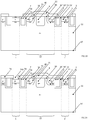
- FIG 5 shows a first embodiment of an inventive power semiconductor device 1 in form of an insulated gate bipolar transistor (IGBT) with a four-layer structure (pnpn).
- the inventive IGBT comprises at least two first cells 1,1', each of which having following layers from a metal emitter electrode 9 on an emitter side 90 and a collector electrode 95 on a collector side 97 opposite to the emitter side 90:
- the metal emitter electrode 9 and the collector electrode 95 are metal electrodes, which may be made of one metal or of a metal alloy or a stack of metals such as aluminium, titanium, chromium, silver, nickel, gold not excluding other electrically conductive metals.
- the inventive device avoids the presence of a polysilicon plate at the emitter electrode 9, i.e. the emitter electrode 9 is a pure metal emitter electrode.
- the inventive IGBT comprises at least one second cell 15 (acting as a dummy cell), which is arranged between two neighboured first cells 1,1' and which has following layers on the emitter side 90:
- An insulator layer stack 75 is arranged on top of the second cell 15 on the emitter side 90 to insulate the second cell 15 and the neighboured trench gate electrodes 7, 7' from the metal emitter electrode 9.
- the insulator layer stack 75 consists of a first insulating layer 73 and a second insulating layer 74, wherein the insulator stack 75 has a thickness on top of the well 8 of a first layer thickness plus the second insulating layer thickness and a thickness on top of the gate layer 70, 70' of the second insulating layer thickness, wherein each thickness of the first and second insulating layer is at least 700 nm (i.e. in total the insulator stack 75 has a thickness on top of the well 8 of at least 1400 nm).
- a capacitance of the layer stack 75 is less than 2.5 nF/cm 2 (which corresponds to an insulating layer stack thickness of 1400 nm).
- the insulating layer stack 75 has a thickness of at least 1400 nm on top of the well and a thickness of at least 700 nm on top of the gate electrodes 7, 7' and on top of the further base layer 30, 30' (at least in a region of the further base layer 30, 30' attached to the gate electrodes 7, 7').
- the insulating layer stack thickness is higher on top of the well 8 than on top of the gate electrodes 7, 7' and further base layer 30, 30'.
- the drift layer 5 extends to the second insulating layer 74 in an area between the well 8 and the further enhancement layers 40, 40'.
- the drift layer 5 has a doping concentration between 1 * 10 12 to 1 * 10 14 cm -3 .
- FIG 6 another inventive IGBT similar to the one shown in FIG 5 is disclosed, which comprises an additional feature of the further enhancement layers 40, 40' adjoining the well layer 8.
- This allows to have a very compact cell structure, i.e. minimizing the space (i.e. width of the second cell 15, which is the extension of the second cell 15 between two first cells 1,1') between the active first cells 1, 1'.
- the enhancement layer 4 and the further enhancement layers 40, 40' have a maximum doping concentration between 5 * 10 15 to 5 * 10 16 cm -3 .
- the enhancement layer 4 and the further enhancement layers 40, 40' may have the same maximum doping concentration.
- the base layer layer 4 and further base layers 40, 40' may extend to the same depth.
- further p doped base layers 30, 30' are arranged in the second cell 15 and adjoin the neighboured trench gate electrodes 7, 7', wherein the further enhancement layers 40, 40' separate the further base layers 30, 30' from the drift layer 5.
- the further base layers 30, 30' may have the same thickness and doping concentration as the base layer 4 and the base layer 4 and further base layers 30, 30' may be manufactured simultaneously.
- the further base layers 30, 30' are drawn in the figures by a dashed line indicating that these layers are optional layers.
- the well 8 has a higher maximum doping concentration than the base layer 3 (and the further base layers 30, 30', if such layers are present).
- the well 8 may have a maximum doping concentration, which is at least a factor of 10 higher than the maximum doping concentration of the base layer 3.
- the well 8 may have a maximum doping concentration of at least 1 * 10 18 cm -3 .
- n doped, further source layers 20, 20' are arranged in the second cell 15 between each further base layer 40, 40' and the second insulating layer 74, which further source layers 20, 20' adjoin the neighboured trench gate electrode 7, 7'.
- the further source layers 20, 20' extend to the emitter sided surface of the device like the source layer 2.
- the source layer 2 and further source layers 20, 20' may be produced simultaneously.
- the further source layers 20, 20' are drawn in the figures by a dashed line indicating that these layers are optional layers.
- each first cell 1,1' has a first cell width 10, which shall be the distance between the two trench gate electrodes 7, 7' of each first cell 1,1' and having a contact to the emitter electrode 9 in between the two trench gate electrodes 7, 7'.
- the first cell width 10 may be smaller than or equal to the gate layer thickness 76 to achieve proper blocking capability. Such a small cell width ensures low losses and a compact design of the device.
- each second cell 15 the well 8 has a well separation distance 82 from the neighboured trench gate electrodes 7, 7', which well separation distance 82 is smaller than or equal to the first cell width 10 (of the neighboured first cells 1, 1').
- An n doped buffer layer 50 with a doping concentration, which is higher than the doping concentration of the drift layer 5 may be arranged between the drift layer 5 and the collector layer 6, so that the n impurity concentration rises from the emitter sided part of the drift layer 5 towards the collector layer 6.
- the buffer layer 50 is drawn in the figures by a dashed line indicating that this layer is an optional layer.
- the inventive emitter sided design can also be applied to a reverse conducting IGBT, in which in the same plane as the collector layer 6 (i.e. on the collector side 97 and lateral to the collector layer 6), an n doped short layer may be arranged.
- the short layer is thus arranged alternating to the collector layer 6.
- the short layer has a higher doping concentration than the drift layer 5.
- the collector layer 6 may comprise p doped regions and the short layer may comprise n doped regions, which regions alternative with each other
- the inventive semiconductor device is suitable for full or part stripes but can also be implemented in cellular designs of the active cells 1, 1'.
- the inventive semiconductor device can comprise a gate electrode design with a different numbers of first cells 1,1' than second cells 15. For example, there may be less second cells 15 than first cells 1, 1' so that the density of active cells 100 versus total area is increased.
- more than one p well 8 is arranged between the active trenches 7, 7' (I,e, between two neighboured active first cells 1, 1'). Between two wells 8, the structure with the further base layer 30, 30' surrounded by the further enhancement layer 40, 40' (or solely the further enhancement layer 40) may be repeated.
- “Lateral” shall mean in this description that two layers/regions are arranged in a same plane, which plane lies parallel to the emitter side. Within that plane the layers are arranged lateral (neighboured, side to side) or adjacent to each other, whereas the layers may have a distance from each other, i.e. another layer may be arranged between the two layers, but they may also be directly adjacent to each other, i.e. in touch to each other. "Lateral sides” of a layer shall be the sides of an object perpendicular to the emitter side 90.
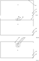
- a well mask 84 is formed having at least one well mask opening 86 on the emitter side 90 ( FIG 10 ).
- the well mask 84 may be formed by applying a continuous layer on the emitter side and then removing material from the well mask 84 to form a well mask opening 86 (or well mask openings), which uncover the wafer in the well mask opening 86.
- the well mask may be made of photoresist.
- the at least one well mask opening 86 is arranged in a central area of a second cell 15 in the finalized IGBT. The p dopant is applied into the wafer on the emitter side 90 at the at least one well mask opening 86.
- the well dopant 85 is then diffused in a heating step, thereby forming the well 8.
- the well mask 84 may be removed before the heating step ( FIG 11 ).
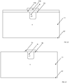
- a first insulating layer 73 is applied having a thickness of at least 700 nm on top of the well 8, which first insulating layer 73 extends over lateral edges of the well 8 ( FIG 13 ).
- the first insulating layer 73 may have a thickness of up to 1200 nm.
- the lower thickness limit is given by the goal to achieve a good insulation between the well 8 and the metal emitter electrode 9 and the upper thickness limit is given by limits in the manufacturing method, i.e. in a single thermal oxidation step the oxide layer can be grown up to about 1200 nm.
- the first insulating layer 73 may be applied by a thermal oxidation step, which oxidation may simultaneously be used for diffusing the p well dopant.
- Such an oxide layer 730 is also called a field oxide layer.
- a thermal oxide layer is formed as a continuous oxide layer over the whole emitter sided surface of the wafer ( FIG 11 ).
- an insulating layer mask 732 has to be applied to remove the oxide layer 730 in areas lateral to the well 8 ( FIG 12 ).
- the well 8 is projected by the remaining field oxide layer (first insulating layer 73) to ensure a good separation of the p well 8 and the further base layer 3 / trench gate electrode 7, 7' in the finalized semiconductor device ( FIG 13 ). Projected shall mean that the first insulating layer 73 is wider than each lateral side/overlaps the well 8 by an overlap distance which is exemplarily at least 3 ⁇ m.
- a trench mask 71 (also called hard mask) is applied having a plurality of trench mask openings 710 on the emitter side 90 laterally to the well 8 and to the first insulating layer 73 ( FIG 14 ).
- a plurality of trench recesses 79, 79' are formed by removing wafer material below the at least two trench mask openings 710. Below refers here to a direction perpendicular to the emitter side 90, i.e. in projection to the trench mask opening 710.
- the trench recesses 79, 79' are etched into the wafer in/below the trench mask openings 710 ( FIG 15 ).
- a gate insulating layer 72, 72' is formed in each trench recess 79, 79', which covers the trench recess walls (lateral trench recess walls and trench recess bottom) ( FIG 16 ). Then a gate layer 70, 70' is formed by filling each trench recess 79, 79' with an electrically conductive material ( FIG 17 ).
- This material may be a polysilicon.
- the polysilicon may be applied as a continuous layer, which is then selectively removed from the wafer surface leaving the polysilicon in the trench recesses 79, 79'.
- the gate layers 70, 70' form together with the surrounding gate insulating layers 72, 72' trench gate electrodes 7, 7'.
- the first insulating layer 73 together with the trench gate electrodes 7, 7' are now used as an enhancement layer mask with the first insulating layer islands 73 acting as absorbing regions. Also in the area of the trench gate electrode 7 (with gate layer 70, 70' and gate insulating layer 72, 72') dopants are absorbed and therefore, no doped layer is formed in the trench gate electrode 7, 7' in the following dopant applying steps.
- n dopant is applied, exemplarily implanted on the emitter side 90.
- "On” in this context shall refer to the dopant being applied onto (in case of dopant deposition) or into (in case of dopant implantation) the emitter sided part of the wafer.
- n dopant is applied as enhancement layer dopant, exemplarily by deposition or implantation, on the emitter side 90 using the first insulating layer 73 and the trench gate electrodes 7, 7' as an enhancement layer mask.
- the enhancement layer dopant is diffused ( FIG 18 ).
- an enhancement layer 4 is formed between two neighboured trench gate electrodes 7, 7' (between which no well is arranged) and a further enhancement layer 40, 40' is arranged between the well 8 and a neighboured gate layer 70, 70'.
- the further enhancement layers 40, 40' may touch the well 8 or they may be separated from the well 8 by the drift layer 5 (part of the wafer 11 with not amended doping concentration).
- a p dopant is applied as base layer dopant, exemplarily by deposition or implantation, on the emitter side 90 using the first insulating layer 73 and the trench gate electrodes 7, 7' as a base layer mask, i.e. the same mask is used for forming the enhancement layers 4, 40, 40' and the base layers 3, 30, 30'.
- the base layer dopant is diffused. Thereby, a base layer 3 is formed between two neighboured trench gate electrodes 7, 7', i.e. in the first cell 1 (between which no well is arranged) and a further base layer 30, 30' is arranged between the well 8 and a neighboured gate layer 70, 70', i.e. in the second cell 15.
- the enhancement layer dopant is further diffused into the wafer than the base layer dopant so that the resulting enhancement layer 4 in the finalized IGBT surrounds the base layer 3 such that the base layer 3 is separated from the drift layer 2 (i.e. the part of the wafer having non amended doping concentration) and the resulting further enhancement layer 40, 40' in the finalized IGBT surrounds the further base layer 30, 30' such that the further base layer 30, 30' is separated from the drift layer 2.
- an n dopant is applied as source layer dopant, exemplarily by deposition or implantation, on the emitter side 90 using the first insulating layer 73 and the trench gate electrodes 7, 7' as a source layer mask (i.e. no further mask is applied) ( FIG 24 ).
- the source layer dopant is diffused.
- a source layer 2 is formed in the first cell 1 between two neighboured trench gate electrodes 7, 7' (between which no well is arranged) and further source layers 20, 20' are formed in the second cell 15 between the trench gate electrodes 7, 7' and the well 8.
- the base layer dopant is further diffused into the wafer than the source layer dopant so that the resulting base layer 3 in the finalized IGBT surrounds the source layer 2 such that the source layer 2 is separated from the enhancement layer 4.
- the further source layer 20, 20' is separated from the well 8 by the further base layer 30, 30' and the further enhancement layer 40, 40'.
- a source layer mask 22 exemplarily a photoresist mask, may be applied in the second cell 15, which covers the whole second cell, i.e. the well 8 and the region between the well 8 and the neighboured trench gate electrodes 7, 7' (i.e. the further base layer 40' and the further enhancement layer 40' and if the drift layer extends to the wafer surface between the well 8 and the further enhancement layer also the drift layer, i.e. the source layer mask 22 covers the layers in the second cell 15) so that no further source layer is formed in the second cell 15 ( FIG 20 ).
- the source layer dopant is applied only in the first cell 1 to form a source layer 2.
- a second insulating layer 74 having a thickness of at least 700 nm is applied, which covers the first insulating layer 73 and extends to and projects the neighboured trench gate electrodes 7, 7', thus the second insulating layer 74 covers the whole second cell 15 and extends further within the first cell 1 so that the second insulating layer 74 projects the trench gate electrodes 7, 7' and is terminated in a region above the source layer 2, but does not completely cover the source layer 2.
- the lower thickness limit is given by the goal to achieve a good insulation between the polysilicon gate electrode and the metal emitter electrode 9 and the upper thickness limit is given by limits in the manufacturing method.
- the second insulating layer 74 has a second insulating layer opening 740 on top of the source layer 2.
- the second insulating layer opening 740 is spaced apart from the neighboured trench gate electrodes 7, 7' so that the source layer 2 is covered by the second insulating layer 74 in a region attached to the neighboured trench gate electrode 7, 7' and the source layer 2 remains at a lateral side of the trench gate electrodes 7, 7' facing away from the well 8.
- the second insulating layer 74 is an inter level dielectric (ILD) layer, which may be formed as a low temperature oxide layer such as a PSG (phosphosilicate glass), BPSG (borophosphosilicate glass) or TEOS (tetra ethyl ortho silicate) layer.
- ILD inter level dielectric
- Such insulating layers can be formed on the wafer by a low temperature process (temperatures between 400 °C and 500 °C) so that the doped layers formed before are not negatively influenced by the temperature when forming the second insulating layer 74.
- the first insulating layer 73 and the second insulating layer 74 form an insulating layer stack 75, which has a thickness on top of the well 8 (thickness of first and second insulating layer), which is higher than its thickness above the trench gate electrodes 7, 7' (thickness of second insulating layer).
- Such an insulating layer stack 75 with different thicknesses enables the device to be manufactured with self-aligned masks. Furthermore, due to the stack being produced by two insulating layers on top of each other it is possible to achieve a higher total thickness on top of the well, by which the capacitance can be reduced to less than 2.5 nF/cm 2 (i.e. with a thickness of at least 1400 nm above the well 8, wherein a thickness of 1400 nm corresponds to a capacitance of 2.5 nF/cm 2 ).
- the opening 740 in the second insulating layer 74 may be formed by applying a mask on top of the second insulating layer with an opening on top of the source layer and spaced apart from the edges of the trench gate electrodes 7, 7'.
- wafer material is etched away down to a depth in the base layer 3, so that below the opening 740 the n doping of the source layer is removed completely, so that the source layer 2 only remains between the lateral sides of the trench gate electrodes 7, 7' and the openings 740 of the second insulating layer 74.
- a metal emitter electrode 9 is formed by applying an electrically conductive material on the emitter side 90 on the second insulating layer 74 and in the second insulating layer opening 740 so that the metal emitter electrode 9 contacts the base layer 3 (in a direction parallel to the emitter side 90, the emitter side 90 being a plane through the top surface of the doped semiconductor layers, which is in this case the top surface of the source layer 2) and the source layer 2 (in a direction perpendicular to the emitter side 90).
- the interface between the metal emitter electrode 9 and the base layer 3 is arranged recessed to the emitter side 90.
- the insulating layer stack 75 is arranged completely below the metal emitter electrode 9 (and all electrically directly connected electrically conductive elements such as the polysilicon plate in prior art devices).
- the full insulating layer stack thickness serves to separate the metal emitter electrode 9 (i.e. all electrically conductive elements put on emitter potential) from the doped layers in the second cell 15.
- the conductivity types are switched, i.e. all layers of the first conductivity type are p type (e.g. the drift layer 5, source layer 2 and enhancement layer 4) and all layers of the second conductivity type are n type (e.g. base layer 3, well 8).
Landscapes
- Thin Film Transistor (AREA)
- Electrodes Of Semiconductors (AREA)
- Thyristors (AREA)
- Metal-Oxide And Bipolar Metal-Oxide Semiconductor Integrated Circuits (AREA)
Abstract
Description
- The invention relates to the field of power semiconductor devices. It relates to an Insulated Gate Bipolar according to the preamble of
claim 1. - Prior art IGBTs having trench MOS cells designs as shown in
FIG 1 have atrench gate electrode 7 with agate layer 70, which is electrically insulated from a p dopedbase layer 3, an n+ dopedsource layer 2 and an n- dopeddrift layer 5 by agate insulating layer 72. Thetrench gate electrode 7 is arranged in the same plane and lateral to thebase layer 3 and extends deeper into thedrift layer 5 than thebase layer 3. - With such trench gate electrode designs, the on-state losses are lower than for planar gate designs, because the trench design offers a vertical MOS channel, which provides enhanced injection of electrons in the vertical direction and suffers from no drawbacks from charge spreading (so called JFET effect) near the cell. Therefore the trench cells show much improved carrier enhancement for lower losses. Due to the vertical channel design, the trench offers also less hole drain effect (PNP effect) due to the improved electron spreading out of the MOS channel than for planar gate designs. At the bottom of the trench there is an accumulation layer, which offers strong charge enhancement for the PIN diode part. Hence wide and/or deep trenches show optimum performance. The trench design offers large cell packing density for reduced channel resistance. The trench design, however, suffers from lower blocking capability near the bottom corners of the trenches due to high peak electric fields. The trench design has a large MOS accumulation region below the trench gate and associated capacitance with difficulty to apply field oxide type layers in the trench for Miller capacitance reduction. Therefore, the prior art device as shown in
FIG 1 results in bad controllability and high switching losses. Furthermore, the high cell densities in trench designs will result in high short circuit currents. - In order to reduce above mentioned effects, the
trench gate electrodes 7 have been made wide and deep, whereas the cells have to be made narrow, so that losses are reduced and short circuit current can be kept low. However, such trenches are difficult to process and will still suffer from bad controllability. - In a further prior art concept shown in
FIG 2 , IGBTs having a pitched-trench gate electrode design has been applied, in which a MOS area is inserted between the cells. The twotrench gate electrodes 7, 7' are connected by alayer 700 made of the same material as thetrench gate electrodes 7, 7', thereby forming an area below, in which a part of thebase layer 3 is arranged, but no source layer or contact of the base layer to the emitter electrode is available in this MOS area. However, such devices result in bad blocking properties and high switching losses due to slow field spreading from the pitched area during switching. - In another approach shown in
FIG 3 ,dummy trench cells 110 have been introduced into another prior art IGBT, in whichactive cells 100, 100' anddummy cells 110 are arranged in an alternating manner. Thebase layer 3 andsource layer 2 do not have a contact to theemitter electrode 9 in thedummy cell 110, However, similar problems to those mentioned for the pitched-trench design apply. - In
US 9105680 B2 FIG 4 ) another prior art IGBT havingtrench gate electrodes 7, 7' is described. Between twoactive trenches 7, 7' a dummy cell 110' is arranged with afurther source layer 20 connected to eachtrench gate electrode 7, 7' and afurther base layer 30 and afurther enhancement layer 40 separating thefurther base layer 40 from thedrift layer 5. In the central part of thedummy cell 110, adeep p well 8 is arranged, which is separated from thefurther base layer 3 by thefurther enhancement layer 40, whichfurther enhancement layer 40 extends to the emitter sided surface of the device. On top of thep well 8, a thin, only 50 to 150 nm thickinsulating film 77 is arranged. Theinsulating film 77 is covered by a groundedpoly silicon plate 78, which is directly connected to theemitter electrode 9 at a recess of the top insulating layer. Due to the thininsulating film 77 the p well capacity is connected to theemitter electrode 9 via the groundedpoly silicon plate 78, the switching capability can be improved. However, in the prior art device known fromUS 9105680 B2 - From
WO 2013/004829 A1 andEP 2 523 217 A1 - Although in
EP 2 523 217 A1 - Moreover in
EP 2 523 217 A1 - It is an object of the invention to provide a power semiconductor device with improved controllability. The problem is solved by the semiconductor device with the characteristics of
claim 1. - The inventive device integrates both active trench and well layers separated from the metal emitter electrode in a dummy cell as a single structure in order to achieve improved controllability performance while maintaining the advantages of reduced on-state and switching losses and improved blocking of the P-well trench IGBT cell. In the inventive design the dummy well layer is only capacitive coupled to the emitter potential and the coupling is weakened by the introduction of a thick insulating layer stack with low capacitance in the dummy region. In addition the presence of the further enhancement layer, having a much larger doping concentration than the drift region, for separating the well from the trench gate electrode in the dummy region, further reduces the amount of holes which can accumulate during the turn-on switching in the dummy cell. Such positive charge can directly connects the gate trench to the P-well and effectively contributes to the Miller capacitance increase.
- By the inventive structure the Miller capacitance contribution of the dummy regions is minimized to improve controllability during turn-on switching.
- Thus, in the inventive device the inversion charge is minimized by reducing the oxide capacitance (due to an increase of the insulating layer stack thickness on top of the well) and by increasing the doping of an n doped layer between the well and the gate electrodes, i.e. by the introduction of a further enhancement layer having a higher doping than the drift layer. These layers can be manufactured using the same or self-aligned masks, in which the first insulating layer serves as mask, in which a dopant is absorbed, whereas in the openings of such insulating layers the dopants can enter into or onto the wafer.
- This structure exploits all the positive effects of the deep well between two active cells for an optimum trade-off among controllability, low switching losses and blocking capability. The enhancement layer itself also has the advantage that the on-state losses are reduced. The inventive IGBT has good electrical properties for both the static and dynamic characteristics.
-
FIG 7 shows turn-on behavior for an inventive device compared to a prior art device as known formFIG 4 . For the voltage, the voltage decreases with a shallower slope for the inventive device. Concerning the collector current Ice, the inventive device shows less overcurrent combined with lower turn-on speed, which leads to a better turn-on controllability.FIG 8 shows the different extent of hole accumulation in the dummy region compared for the inventive and prior art device during the turn on switching, after the gate voltage has risen over the Vth value and the IGBT starts to conduct. On the left handed side of the figure, the charge rises from the surface of the gate insulating layer, on the right handed side of the figure, the charge saturates within the well. The inventive device proves to have a tremendous reduction of hole current density (charge) in the dummy cell area. - The proposed structure and its manufacturing process are advantageous in providing full flexibility in designing the dielectric thickness stack (insulating layer stack) to decouple the emitter metal.
- The inventive design is suitable for full or part stripes but can also be implemented in cellular designs.
- Further advantages according to the present invention will be apparent from the dependent claims.
- The subject matter of the invention will be explained in more detail in the following text with reference to the attached drawings, in which:
- FIG 1
- shows an IGBT with a trench gate electrode according to the prior art;
- FIG 2
- shows another IGBT with a pitched trench gate electrode according to the prior art;
- FIG 3
- shows another IGBT with a dummy cell according to the prior art;
- FIG 4
- shows another IGBT with a dummy cell according to the prior art;
- FIG 5
- shows a first exemplary embodiment of an IGBT according to the invention;
- FIG 6
- show another exemplary embodiment of an IGBT according to the invention;
- FIG 7
- shows voltage and current for an inventive device and the prior art device as known from
FIG 4 ; - FIG 8
- shows hole current density at the maximum Ice current slope dlce/dt during the turn-on switching in a region just below the second insulating layer in the second cell area as indicated in
FIG 5 by the dashed oval line; and - FIG 9 to 23
- shows steps of a methods of manufacturing an inventive IGBT;
- FIG 24
- shows an alternative step in an inventive method of manufacturing an inventive IGBT.
- The reference symbols used in the figures and their meaning are summarized in the list of reference symbols. Generally, alike or alike-functioning parts are given the same reference symbols. The described embodiments are meant as examples and shall not confine the invention.
-
FIG 5 shows a first embodiment of an inventivepower semiconductor device 1 in form of an insulated gate bipolar transistor (IGBT) with a four-layer structure (pnpn). The inventive IGBT comprises at least twofirst cells 1,1', each of which having following layers from ametal emitter electrode 9 on anemitter side 90 and acollector electrode 95 on acollector side 97 opposite to the emitter side 90: - an n doped source layer 2 (n being in this example a first conductivity type). The
first source layer 2 has a higher doping concentration than adrift layer 5. - a p doped base layer 3 (p being in this example a second conductivity type, which is different from the first conductivity type), wherein the
source layer 2 and thebase layer 3 contact themetal emitter electrode 9. Thesource layer 2 is arranged on thebase layer 3, which shall mean that thesource layer 2 is arranged at the surface of the device at theemitter side 90. Thesource layer 2 may be embedded in thebase layer 3 towards the bottom side and lateral sides such that both layers have a common surface on theemitter side 90 or thesource layer 2 may be arranged on thebase layer 3, it may be arranged completely on top of thebase layer 3 such that the bottom side of thesource layer 2 touches the top side of thebase layer 3 towards theemitter side 90. - an n doped
enhancement layer 4 having higher doping concentration than thedrift layer 5, wherein thebase layer 3 separates thesource layer 2 from theenhancement layer 4, - an n- doped
drift layer 5, wherein theenhancement layer 4 separates thebase layer 3 from thedrift layer 5. Exemplarily, thedrift layer 5 has a constant, uniform low doping concentration. - a p doped
collector layer 6, which is arranged between thedrift layer 5 and thecollector electrode 95 and which electrically contacts thecollector electrode 95, - two
trench gate electrodes 7, 7', each of which comprises an electricallyconductive gate layer 70, 70', which is arranged lateral to thebase layer 3, extends deeper into thedrift layer 5 than thebase layer 3 and has agate layer thickness 76, and agate insulating layer 72, 72', which separates thegate layer 70, 70' from any doped layer (i.e. thesource layer 2, thebase layer 3, theenhancement layer 4 and the drift layer 5). A MOS channel is formable between thesource layer 2, thebase layer 3, theenhancement layer 4 and thedrift layer 5. Thetrench gate electrodes 7, 7' may have any design well-known to the experts like cellular design, full or part stripes. - The
metal emitter electrode 9 and thecollector electrode 95 are metal electrodes, which may be made of one metal or of a metal alloy or a stack of metals such as aluminium, titanium, chromium, silver, nickel, gold not excluding other electrically conductive metals. The inventive device avoids the presence of a polysilicon plate at theemitter electrode 9, i.e. theemitter electrode 9 is a pure metal emitter electrode. - The inventive IGBT comprises at least one second cell 15 (acting as a dummy cell), which is arranged between two neighboured
first cells 1,1' and which has following layers on the emitter side 90: - a p+ doped well 8, which is arranged between two
trench gate electrodes 7, 7' of the neighbouredfirst cells 1, 1', which well 8 has awell thickness 80, which extends at least to thegate layer thickness 76, i.e. thewell 8 extends in depth direction, which shall lie perpendicular to theemitter side 90, at least to such depth, to which the deepest gate layers 70, 70' extend. Exemplarily, thewell 8 extends to a greater depth than the gate layers 70, 70'. - n doped further enhancement layers 40, 40', which have a higher doping concentration than the
drift layer 5 and which are arranged between thewell 8 and each of the two neighbouredtrench gate electrodes 7, 7' (of the neighbouredfirst cells 1, 1') such that the further enhancement layers 40, 40' extend to theemitter side 90. Exemplarily, the further enhancement layers 40, 40' are shallower than thewell 8. The further enhancement layers 40, 40' prevent that the holes accumulate in the dummy cell. The further enhancement layers 40, 40' extends from the neighbouredtrench gate electrodes 7, 7' (i.e. from their side walls) to the firstmain side 90 between thewell 8 and saidtrench gate electrode 7, 7'. - An
insulator layer stack 75 is arranged on top of thesecond cell 15 on theemitter side 90 to insulate thesecond cell 15 and the neighbouredtrench gate electrodes 7, 7' from themetal emitter electrode 9. Theinsulator layer stack 75 consists of a first insulatinglayer 73 and a second insulatinglayer 74, wherein theinsulator stack 75 has a thickness on top of thewell 8 of a first layer thickness plus the second insulating layer thickness and a thickness on top of thegate layer 70, 70' of the second insulating layer thickness, wherein each thickness of the first and second insulating layer is at least 700 nm (i.e. in total theinsulator stack 75 has a thickness on top of thewell 8 of at least 1400 nm). By such a thick insulating layer stack, a capacitance of thelayer stack 75 is less than 2.5 nF/cm2 (which corresponds to an insulating layer stack thickness of 1400 nm). Such a low capacitance of the insulatinglayer stack 75 ensures a good electrical insulation towards themetal emitter electrode 9 to prevent a capacitive coupling to themetal emitter electrode 9. The insulatinglayer stack 75 has a thickness of at least 1400 nm on top of the well and a thickness of at least 700 nm on top of thegate electrodes 7, 7' and on top of thefurther base layer 30, 30' (at least in a region of thefurther base layer 30, 30' attached to thegate electrodes 7, 7'). Thus, the insulating layer stack thickness is higher on top of thewell 8 than on top of thegate electrodes 7, 7' andfurther base layer 30, 30'. - In the inventive IGBT shown in
FIG 5 thedrift layer 5 extends to the second insulatinglayer 74 in an area between thewell 8 and the further enhancement layers 40, 40'. In another exemplary embodiment, thedrift layer 5 has a doping concentration between 1 * 1012 to 1 * 1014 cm-3. - In the
FIG 6 another inventive IGBT similar to the one shown inFIG 5 is disclosed, which comprises an additional feature of the further enhancement layers 40, 40' adjoining thewell layer 8. This allows to have a very compact cell structure, i.e. minimizing the space (i.e. width of thesecond cell 15, which is the extension of thesecond cell 15 between twofirst cells 1,1') between the activefirst cells 1, 1'. - In another exemplary embodiment, the
enhancement layer 4 and the further enhancement layers 40, 40' have a maximum doping concentration between 5 * 1015 to 5 * 1016 cm-3. Theenhancement layer 4 and the further enhancement layers 40, 40' may have the same maximum doping concentration. Thebase layer layer 4 and further base layers 40, 40' may extend to the same depth. - In another inventive embodiment, further p doped base layers 30, 30' are arranged in the
second cell 15 and adjoin the neighbouredtrench gate electrodes 7, 7', wherein the further enhancement layers 40, 40' separate the further base layers 30, 30' from thedrift layer 5. The further base layers 30, 30' may have the same thickness and doping concentration as thebase layer 4 and thebase layer 4 and further base layers 30, 30' may be manufactured simultaneously. The further base layers 30, 30' are drawn in the figures by a dashed line indicating that these layers are optional layers. - The
well 8 has a higher maximum doping concentration than the base layer 3 (and the further base layers 30, 30', if such layers are present). Thewell 8 may have a maximum doping concentration, which is at least a factor of 10 higher than the maximum doping concentration of thebase layer 3. In an exemplary embodiment, thewell 8 may have a maximum doping concentration of at least 1 * 1018 cm-3. - In another exemplary embodiment, n doped, further source layers 20, 20' are arranged in the
second cell 15 between eachfurther base layer 40, 40' and the second insulatinglayer 74, which further source layers 20, 20' adjoin the neighbouredtrench gate electrode 7, 7'. The further source layers 20, 20' extend to the emitter sided surface of the device like thesource layer 2. Thesource layer 2 and further source layers 20, 20' may be produced simultaneously. The further source layers 20, 20' are drawn in the figures by a dashed line indicating that these layers are optional layers. - In another exemplary embodiment, each
first cell 1,1' has afirst cell width 10, which shall be the distance between the twotrench gate electrodes 7, 7' of eachfirst cell 1,1' and having a contact to theemitter electrode 9 in between the twotrench gate electrodes 7, 7'. Thefirst cell width 10 may be smaller than or equal to thegate layer thickness 76 to achieve proper blocking capability. Such a small cell width ensures low losses and a compact design of the device. - In another exemplary embodiment, in each
second cell 15 thewell 8 has awell separation distance 82 from the neighbouredtrench gate electrodes 7, 7', which wellseparation distance 82 is smaller than or equal to the first cell width 10 (of the neighbouredfirst cells 1, 1'). This also results in a compact design of the device and provides proper blocking capability. An n dopedbuffer layer 50 with a doping concentration, which is higher than the doping concentration of thedrift layer 5 may be arranged between thedrift layer 5 and thecollector layer 6, so that the n impurity concentration rises from the emitter sided part of thedrift layer 5 towards thecollector layer 6. Thebuffer layer 50 is drawn in the figures by a dashed line indicating that this layer is an optional layer. - The inventive emitter sided design can also be applied to a reverse conducting IGBT, in which in the same plane as the collector layer 6 (i.e. on the
collector side 97 and lateral to the collector layer 6), an n doped short layer may be arranged. The short layer is thus arranged alternating to thecollector layer 6. The short layer has a higher doping concentration than thedrift layer 5. Thecollector layer 6 may comprise p doped regions and the short layer may comprise n doped regions, which regions alternative with each other - The inventive semiconductor device is suitable for full or part stripes but can also be implemented in cellular designs of the
active cells 1, 1'. - Exemplarily, the inventive semiconductor device can comprise a gate electrode design with a different numbers of
first cells 1,1' thansecond cells 15. For example, there may be lesssecond cells 15 thanfirst cells 1, 1' so that the density ofactive cells 100 versus total area is increased. In another alternative, more than onep well 8 is arranged between theactive trenches 7, 7' (I,e, between two neighboured activefirst cells 1, 1'). Between twowells 8, the structure with thefurther base layer 30, 30' surrounded by thefurther enhancement layer 40, 40' (or solely the further enhancement layer 40) may be repeated. - "Lateral" shall mean in this description that two layers/regions are arranged in a same plane, which plane lies parallel to the emitter side. Within that plane the layers are arranged lateral (neighboured, side to side) or adjacent to each other, whereas the layers may have a distance from each other, i.e. another layer may be arranged between the two layers, but they may also be directly adjacent to each other, i.e. in touch to each other. "Lateral sides" of a layer shall be the sides of an object perpendicular to the
emitter side 90. - For manufacturing an inventive insulated gated bipolar transistor the following manufacturing steps are performed:
- (a) providing a lowly n- doped
wafer 11 having anemitter side 90 and acollector side 97 opposite to the emitter side 90 (FIG 9 ), - (b) forming a
well mask 84 having at least onewell mask opening 86 on theemitter side 90,
applying a p dopant as welldopant 85 on theemitter side 90 through the at least one well mask opening 86 (FIG 10 ), - (c) removing the
well mask 84, - (d) after step (b) and before a step (e) forming a well 8 by diffusing the well dopant (
FIG 1 ), - (e) applying a first insulating
layer 73 having a thickness of at least 700 nm on top of thewell 8, which projects, i.e. extends over lateral edges of the well 8 (FIG 13 ), - (f) applying a
trench mask 71 having a plurality oftrench mask openings 710, 710' on theemitter side 90 in a region lateral to and being spaced apart from the well 8 (FIG 14 ),
forming a plurality of trench recesses 79, 79' by removing wafer material below the plurality oftrench mask openings 710, 710' (FIG 15 ), forming agate insulating layer 72, 72' in eachtrench recess 79, 79' covering thetrench recess walls 79, 79' (FIG 16 ), forming agate layer 70, 70' in eachtrench recess 79, 79' by filling eachtrench recess 79, 79' with an electrically conductive material (FIG 17 ), thereby forming a plurality oftrench gate electrodes 7, 7' comprising the gate layers 70, 70' and thegate insulating layers 72, 72', - (g) forming an
enhancement layer 4 between twotrench gate electrodes 70, 70' (having no well inbetween) and afurther enhancement layer 40, 40' between thewell 8 and a neighbouredtrench gate electrode 7, 7' by applying an enhancement layer dopant (n dopant) on theemitter side 90 using the first insulatinglayer 73 and thetrench gate electrodes 7, 7' as an enhancement layer mask and diffusing the enhancement layer dopant (FIG 18 ), - (h) forming a
base layer 3 between between twotrench gate electrodes 7, 7' (having no well inbetween) and afurther base layer 30, 30' between thewell 8 and a neighbouredtrench gate electrode 7, 7' by applying a p dopant as base layer dopant on theemitter side 90 using the first insulating layer (73, 73') and the plurality of trench gate electrodes (7, 7') as a base layer mask and diffusing the base layer dopant to a lower depth than the enhancement layer dopant has been diffused so that thebase layer 3 and thefurther base layer 30, 30' are separated from thedrift layer 5 by theenhancement layer 4 and thefurther enhancement layer 40, 40' respectively (FIG 19 ), - (i) forming a
source layer 2 by applying an n dopant as source layer dopant on theemitter side 90 using the first insulating layer 73 (and thetrench gate electrodes 7, 7') as a source layer mask and diffusing the source layer dopant (FIG 20 orFIG 24 ), - (j) applying a second insulating
layer 74 having a thickness of at least 700 nm, which covers the first insulatinglayer 73 and extends to and projects the neighbouredtrench gate electrodes 7, 7', wherein the second insulatinglayer 74 has a second insulating layer opening 740 on top of thesource layer 2, which second insulatinglayer opening 740 is spaced apart from the edges of the neighbouredtrench gate electrodes 7, 7' so that thesource layer 2 remains at a lateral side of thetrench gate electrodes 7, 7' facing away from thewell 8, wherein the first insulatinglayer 73 and the second insulatinglayer 74 form an insulatinglayer stack 75, which has a thickness on top of thewell 8 of a first insulating layer thickness and a second insulating layer thickness and a thickness on top of thegate layer 70, 70' of the second insulating layer thickness (i.e. without the first insulating thickness) (FIG 21 ), - (k) removing wafer material (i.e. from the source layer) at least to a depth of the
base layer 3 using the second insulatinglayer 74 with the second insulatinglayer opening 740 as an emitter electrode mask (FIG 21 ) so that thesource layer 2 remains at the lateral sides of thetrench gate electrodes 7, 7' and thesource layer 2 attaches thetrench gate electrodes 7, 7',
forming ametal emitter electrode 9 by applying an electrically conductive material on theemitter side 90 in the second insulatinglayer opening 740 so that themetal emitter electrode 9 contacts thebase layer 3 and the source layer 2 (FIG 22 ). - In step (b) a
well mask 84 is formed having at least onewell mask opening 86 on the emitter side 90 (FIG 10 ). Thewell mask 84 may be formed by applying a continuous layer on the emitter side and then removing material from thewell mask 84 to form a well mask opening 86 (or well mask openings), which uncover the wafer in thewell mask opening 86. The well mask may be made of photoresist. The at least onewell mask opening 86 is arranged in a central area of asecond cell 15 in the finalized IGBT. The p dopant is applied into the wafer on theemitter side 90 at the at least onewell mask opening 86. - The
well dopant 85 is then diffused in a heating step, thereby forming thewell 8. Thewell mask 84 may be removed before the heating step (FIG 11 ). - Afterwards, a first insulating
layer 73 is applied having a thickness of at least 700 nm on top of thewell 8, which first insulatinglayer 73 extends over lateral edges of the well 8 (FIG 13 ). The first insulatinglayer 73 may have a thickness of up to 1200 nm. The lower thickness limit is given by the goal to achieve a good insulation between thewell 8 and themetal emitter electrode 9 and the upper thickness limit is given by limits in the manufacturing method, i.e. in a single thermal oxidation step the oxide layer can be grown up to about 1200 nm. The first insulatinglayer 73 may be applied by a thermal oxidation step, which oxidation may simultaneously be used for diffusing the p well dopant. Such anoxide layer 730 is also called a field oxide layer. A thermal oxide layer is formed as a continuous oxide layer over the whole emitter sided surface of the wafer (FIG 11 ). For afield oxide layer 730, an insulatinglayer mask 732 has to be applied to remove theoxide layer 730 in areas lateral to the well 8 (FIG 12 ). Thewell 8 is projected by the remaining field oxide layer (first insulating layer 73) to ensure a good separation of the p well 8 and thefurther base layer 3 /trench gate electrode 7, 7' in the finalized semiconductor device (FIG 13 ). Projected shall mean that the first insulatinglayer 73 is wider than each lateral side/overlaps thewell 8 by an overlap distance which is exemplarily at least 3 µm. - Now, a trench mask 71 (also called hard mask) is applied having a plurality of
trench mask openings 710 on theemitter side 90 laterally to thewell 8 and to the first insulating layer 73 (FIG 14 ). A plurality of trench recesses 79, 79' are formed by removing wafer material below the at least twotrench mask openings 710. Below refers here to a direction perpendicular to theemitter side 90, i.e. in projection to thetrench mask opening 710. Exemplarily, the trench recesses 79, 79' are etched into the wafer in/below the trench mask openings 710 (FIG 15 ). Agate insulating layer 72, 72' is formed in eachtrench recess 79, 79', which covers the trench recess walls (lateral trench recess walls and trench recess bottom) (FIG 16 ). Then agate layer 70, 70' is formed by filling eachtrench recess 79, 79' with an electrically conductive material (FIG 17 ). This material may be a polysilicon. The polysilicon may be applied as a continuous layer, which is then selectively removed from the wafer surface leaving the polysilicon in the trench recesses 79, 79'. Optionally, there may also polysilicon remain at an edge of a first cells 1 (active cells) for a contact of the gate layers 70, 70' to a gate runner. The gate layers 70, 70' form together with the surroundinggate insulating layers 72, 72'trench gate electrodes 7, 7'. - The first insulating
layer 73 together with thetrench gate electrodes 7, 7' are now used as an enhancement layer mask with the first insulatinglayer islands 73 acting as absorbing regions. Also in the area of the trench gate electrode 7 (withgate layer 70, 70' andgate insulating layer 72, 72') dopants are absorbed and therefore, no doped layer is formed in thetrench gate electrode 7, 7' in the following dopant applying steps. - An n dopant is applied, exemplarily implanted on the
emitter side 90. "On" in this context shall refer to the dopant being applied onto (in case of dopant deposition) or into (in case of dopant implantation) the emitter sided part of the wafer. - An n dopant is applied as enhancement layer dopant, exemplarily by deposition or implantation, on the
emitter side 90 using the first insulatinglayer 73 and thetrench gate electrodes 7, 7' as an enhancement layer mask. Afterwards, the enhancement layer dopant is diffused (FIG 18 ). Thereby, anenhancement layer 4 is formed between two neighbouredtrench gate electrodes 7, 7' (between which no well is arranged) and afurther enhancement layer 40, 40' is arranged between thewell 8 and aneighboured gate layer 70, 70'. Depending on the width, by which the first insulating layer projects thewell 8 and by the diffusion conditions, the further enhancement layers 40, 40' may touch thewell 8 or they may be separated from the well 8 by the drift layer 5 (part of thewafer 11 with not amended doping concentration). - A p dopant is applied as base layer dopant, exemplarily by deposition or implantation, on the
emitter side 90 using the first insulatinglayer 73 and thetrench gate electrodes 7, 7' as a base layer mask, i.e. the same mask is used for forming the enhancement layers 4, 40, 40' and the base layers 3, 30, 30'. Afterwards, the base layer dopant is diffused. Thereby, abase layer 3 is formed between two neighbouredtrench gate electrodes 7, 7', i.e. in the first cell 1 (between which no well is arranged) and afurther base layer 30, 30' is arranged between thewell 8 and aneighboured gate layer 70, 70', i.e. in thesecond cell 15. The enhancement layer dopant is further diffused into the wafer than the base layer dopant so that the resultingenhancement layer 4 in the finalized IGBT surrounds thebase layer 3 such that thebase layer 3 is separated from the drift layer 2 (i.e. the part of the wafer having non amended doping concentration) and the resultingfurther enhancement layer 40, 40' in the finalized IGBT surrounds thefurther base layer 30, 30' such that thefurther base layer 30, 30' is separated from thedrift layer 2. - Afterwards, an n dopant is applied as source layer dopant, exemplarily by deposition or implantation, on the
emitter side 90 using the first insulatinglayer 73 and thetrench gate electrodes 7, 7' as a source layer mask (i.e. no further mask is applied) (FIG 24 ). Afterwards, the source layer dopant is diffused. Thereby, asource layer 2 is formed in thefirst cell 1 between two neighbouredtrench gate electrodes 7, 7' (between which no well is arranged) and further source layers 20, 20' are formed in thesecond cell 15 between thetrench gate electrodes 7, 7' and thewell 8. The base layer dopant is further diffused into the wafer than the source layer dopant so that the resultingbase layer 3 in the finalized IGBT surrounds thesource layer 2 such that thesource layer 2 is separated from theenhancement layer 4. In thesecond cell 15, thefurther source layer 20, 20' is separated from the well 8 by thefurther base layer 30, 30' and thefurther enhancement layer 40, 40'. - Before applying the source dopant, a
source layer mask 22, exemplarily a photoresist mask, may be applied in thesecond cell 15, which covers the whole second cell, i.e. thewell 8 and the region between thewell 8 and the neighbouredtrench gate electrodes 7, 7' (i.e. the further base layer 40' and the further enhancement layer 40' and if the drift layer extends to the wafer surface between thewell 8 and the further enhancement layer also the drift layer, i.e. thesource layer mask 22 covers the layers in the second cell 15) so that no further source layer is formed in the second cell 15 (FIG 20 ). In this case, the source layer dopant is applied only in thefirst cell 1 to form asource layer 2. - Now, a second insulating
layer 74 having a thickness of at least 700 nm is applied, which covers the first insulatinglayer 73 and extends to and projects the neighbouredtrench gate electrodes 7, 7', thus the second insulatinglayer 74 covers the wholesecond cell 15 and extends further within thefirst cell 1 so that the second insulatinglayer 74 projects thetrench gate electrodes 7, 7' and is terminated in a region above thesource layer 2, but does not completely cover thesource layer 2. The lower thickness limit is given by the goal to achieve a good insulation between the polysilicon gate electrode and themetal emitter electrode 9 and the upper thickness limit is given by limits in the manufacturing method. The second insulatinglayer 74 has a second insulating layer opening 740 on top of thesource layer 2. The secondinsulating layer opening 740 is spaced apart from the neighbouredtrench gate electrodes 7, 7' so that thesource layer 2 is covered by the second insulatinglayer 74 in a region attached to the neighbouredtrench gate electrode 7, 7' and thesource layer 2 remains at a lateral side of thetrench gate electrodes 7, 7' facing away from thewell 8. Exemplarily, the second insulatinglayer 74 is an inter level dielectric (ILD) layer, which may be formed as a low temperature oxide layer such as a PSG (phosphosilicate glass), BPSG (borophosphosilicate glass) or TEOS (tetra ethyl ortho silicate) layer. Such insulating layers can be formed on the wafer by a low temperature process (temperatures between 400 °C and 500 °C) so that the doped layers formed before are not negatively influenced by the temperature when forming the second insulatinglayer 74. - The first insulating
layer 73 and the second insulatinglayer 74 form an insulatinglayer stack 75, which has a thickness on top of the well 8 (thickness of first and second insulating layer), which is higher than its thickness above thetrench gate electrodes 7, 7' (thickness of second insulating layer). Such an insulatinglayer stack 75 with different thicknesses enables the device to be manufactured with self-aligned masks. Furthermore, due to the stack being produced by two insulating layers on top of each other it is possible to achieve a higher total thickness on top of the well, by which the capacitance can be reduced to less than 2.5 nF/cm2 (i.e. with a thickness of at least 1400 nm above thewell 8, wherein a thickness of 1400 nm corresponds to a capacitance of 2.5 nF/cm2). - The
opening 740 in the second insulatinglayer 74 may be formed by applying a mask on top of the second insulating layer with an opening on top of the source layer and spaced apart from the edges of thetrench gate electrodes 7, 7'. - Then wafer material is etched away down to a depth in the
base layer 3, so that below theopening 740 the n doping of the source layer is removed completely, so that thesource layer 2 only remains between the lateral sides of thetrench gate electrodes 7, 7' and theopenings 740 of the second insulatinglayer 74. Now ametal emitter electrode 9 is formed by applying an electrically conductive material on theemitter side 90 on the second insulatinglayer 74 and in the second insulatinglayer opening 740 so that themetal emitter electrode 9 contacts the base layer 3 (in a direction parallel to theemitter side 90, theemitter side 90 being a plane through the top surface of the doped semiconductor layers, which is in this case the top surface of the source layer 2) and the source layer 2 (in a direction perpendicular to the emitter side 90). Thus, the interface between themetal emitter electrode 9 and thebase layer 3 is arranged recessed to theemitter side 90. - There is no insulating layer arranged on the wafer, which is sandwiched between two parts of the metal emitter electrode (which could lead to voltage drops in the metal emitter electrode). The insulating
layer stack 75 is arranged completely below the metal emitter electrode 9 (and all electrically directly connected electrically conductive elements such as the polysilicon plate in prior art devices). The full insulating layer stack thickness serves to separate the metal emitter electrode 9 (i.e. all electrically conductive elements put on emitter potential) from the doped layers in thesecond cell 15. - In another embodiment, the conductivity types are switched, i.e. all layers of the first conductivity type are p type (e.g. the
drift layer 5,source layer 2 and enhancement layer 4) and all layers of the second conductivity type are n type (e.g. base layer 3, well 8). - It should be noted that the term "comprising" does not exclude other elements or steps and that the indefinite article "a" or "an" does not exclude the plural. Also elements described in association with different embodiments may be combined. It should also be noted that reference signs in the claims shall not be construed as limiting the scope of the claims.
-
- 1, 1'
- first cell
- 10
- first cell width
- 11
- wafer
- 15
- second cell
- 100
- active cell
- 110, 110'
- dummy cell
- 2
- source layer
- 20, 20'
- further source layer
- 22
- source layer mask
- 3
- base layer
- 30, 30'
- further base layer
- 4
- enhancement layer
- 40, 40'
- further enhancement layer
- 5
- drift layer
- 50
- buffer layer
- 6
- collector layer
- 7, 7'
- trench gate electrode
- 70, 70'
- gate layer
- 700
- layer
- 71
- trench mask
- 710
- trench mask opening
- 72, 72'
- gate insulating layer
- 73
- first insulating layer
- 730
- oxide layer
- 732
- insulating layer mask
- 74
- second insulating layer
- 740
- second insulating layer opening
- 75
- insulating layer stack
- 76
- gate layer thickness
- 77
- insulating film
- 78
- poly silicon plate
- 79
- trench recess
- 8
- well
- 80
- well layer thickness
- 82
- well separation distance
- 84
- well mask
- 86
- well mask opening
- 9
- metal emitter electrode
- 90
- emitter side
- 95
- collector electrode
- 97
- collector side
Claims (13)
- An insulated gated bipolar transistor comprising at least two first cells (1, 1'), each of which having following layers from a metal emitter electrode (9) on an emitter side (90) and a collector electrode (95) on a collector side (97) opposite to the emitter side (90):- a source layer (2) of a first conductivity type,- a base layer (3) of a second conductivity type, which is different from the first conductivity type, wherein the source layer (2) and the base layer (3) contact the metal emitter electrode (9),- an enhancement layer (4) of the first conductivity type having higher doping concentration than the drift layer (5), wherein the base layer (3) separates the source layer (2) from the enhancement layer (4),- a drift layer (5) of the first conductivity type, wherein the enhancement layer (4) separates the base layer (3) from the drift layer (5),- a collector layer (6) of the second conductivity type, which is arranged between the drift layer (5) and the collector electrode (95) and which electrically contacts the collector electrode (95),- two trench gate electrodes (7, 7'), each of which comprises an electrically conductive gate layer (70, 70'), which is arranged lateral to the base layer (3), extends deeper into the drift layer (5) than the base layer (3) and has a gate layer thickness (76), and a gate insulating layer (72, 72'), which separates the gate layer (70, 70') from any doped layer,
wherein a channel is formable between the source layer (2), the base layer (3), the enhancement layer (4) and the drift layer (5),- the insulated gated bipolar transistor comprising at least one second cell (15) which is arranged between two neighboured first cells (1, 1') and which has following layer on the emitter side (90):
a well (8) of the second conductivity type, which is arranged between two trench gate electrodes (7, 7') of the neighboured first cells (1, 1'), which well (8) extends at least to the gate layer thickness (76), characterized in, that- further enhancement layers (40, 40') of the first conductivity type having higher doping concentration than the drift layer (5) are arranged between the well (8) and the neighboured trench gate electrodes (7, 7') such that the further enhancement layers (40, 40') extend to the emitter side (90),- an insulator layer stack (75) is arranged on top of the second cell (15) on the emitter side (90) to insulate the second cell (15) and the neighboured trench gate electrodes (7, 7') from the metal emitter electrode (9), which consists of a first insulating layer (73) and a second insulating layer (74), wherein the insulator stack (75) has a thickness on top of the well (8) of a first layer thickness plus the second insulating layer thickness and a thickness on top of the gate layer (70, 70') of the second insulating layer thickness, wherein each thickness of the first insulating layer (73) and the second insulating layer (74) is at least 700 nm. - The insulated gated bipolar transistor according to claim 1, characterized in, that the further enhancement layers (40, 40') adjoin the well (8) so that the drift layer (5) is separated from the second insulating layer (74) in the second cell (15) by the further enhancement layer (40, 40').
- The insulated gated bipolar transistor according to claim 1, characterized in, that the drift layer (5) extends to the second insulating layer (74) in an area between the well (8) and the further enhancement layers (40, 40').
- The insulated gated bipolar transistor according to any of the claims 1 to 3, characterized in, that further base layers (30, 30') of the second conductivity type are arranged in the second cell (15) and adjoin the neighboured trench gate electrodes (7, 7'), wherein the further enhancement layers (40, 40') separate the further base layers (30, 30') from the drift layer (5).
- The insulated gated bipolar transistor according to claim 4, characterized in, that further source layers (20, 20') of the first conductivity type are arranged in the second cell (15) between the further base layer (40, 40') and the second insulating layer (74), which further source layers (20, 20') adjoin the neighboured trench gate electrodes (7, 7').
- The insulated gated bipolar transistor according to any of the claims 1 to 5, characterized in, that each first cell (1, 1') has a first cell width (10) between the two trench gate electrodes (7, 7') of the first cell (1, 1'), wherein the first cell width (10) is smaller than or equal to the gate layer thickness (76).
- The insulated gated bipolar transistor according to any of the claims 1 to 6, characterized in, that in each second cell (15) the well (8) has a well separation distance (82) from the neighboured trench gate electrodes (7, 7'), which well separation distance (82) is smaller than or equal to the first cell width (10).
- The insulated gated bipolar transistor according to any of the claims 1 to 7, characterized in, that a buffer layer (50) of the first conductivity type having a higher doping concentration than the drift layer (5) is arranged between the drift layer (5) and the collector layer (6).
- The insulated gated bipolar transistor according to any of the claims 1 to 8, characterized in, that the insulated gated bipolar transistor further comprises a short layer of the first conductivity type, which is arranged on the collector side (97) laterally to the collector layer (6), which short layer has a higher doping concentration than the drift layer (5).
- The insulated gated bipolar transistor according to any of the claims 1 to 9, characterized in, that the enhancement layer (4) and the further enhancement layers (40, 40') have a maximum doping concentration between 5 * 1015 to 5 * 1016 cm-3.
- The insulated gated bipolar transistor according to any of the claims 1 to 10, characterized in, that the well (8) has a maximum doping concentration of at least 1 * 1018 cm-3.
- The insulated gated bipolar transistor according to any of the claims 1 to 11, characterized in, that the well (8) has a maximum doping concentration, which is at least a factor of 10 higher than the maximum doping concentration of the base layer (3).
- A method of manufacturing an insulated gated bipolar transistor according to any of the claims 1 to 12 having the following manufacturing steps:(a) providing a wafer (11) of a first conductivity type having an emitter side (90) and a collector side (97) opposite to the emitter side (90),(b) forming a well mask (84) having at least one well mask opening (86) on the emitter side (90),
applying a well dopant (85) of a second conductivity type which is different from the first conductivity type through the at least one well mask opening (86),(c) removing the well mask (84),(d) after step (b) and before a step (e) forming a well (8) by diffusing the well dopant (85),(e) applying a first insulating layer (73) having a thickness of at least 700 nm on top of the well (8), which extends over lateral edges of the well (8),(f) applying a trench mask (71) having a plurality of trench mask openings (710) on the emitter side (90),
forming a trench recess (79) by removing wafer material in each trench mask opening (710),
forming a gate insulating layer (72, 72') in each trench recess (79) covering the trench recess walls (790),
forming a gate layer (70, 70') in each trench recess (79) by filling each trench recess (79) with an electrically conductive material, thereby forming a plurality of trench gate electrodes (7, 7') comprising the gate layers (70, 70') and the gate insulating layers (72, 72'),(g) forming an enhancement layer (4) between two trench gate electrodes (7, 7') and a further enhancement layer (40, 40') between the well (8) and a neighboured trench gate electrode (7, 7') by applying an enhancement layer dopant of the first conductivity type on the emitter side (90) using the first insulating layer (73, 73') and the plurality of trench gate electrodes (7, 7') as an enhancement layer mask and diffusing the enhancement layer dopant,(h) forming a base layer (3) between two trench gate electrodes (7, 7') and a further base layer (30, 30') between the well (8) and a neighboured trench gate electrode (7, 7') by applying a base layer dopant of the second conductivity type on the emitter side (90) and diffusing the base layer dopant using the first insulating layer (73, 73') and the plurality of trench gate electrodes (7, 7') as a base layer mask,(i) forming a source layer (2) by applying a source layer dopant of the first conductivity type on the emitter side (90) and diffusing the source layer dopant using at least the first insulating layer (73, 73') and the plurality of trench gate electrodes (7, 7') as a source layer mask,(j) applying a second insulating layer (74) having a thickness of at least 700 nm, which covers the first insulating layer (73) and extends to and projects the neighboured trench gate electrodes (70, 70') and having at least one second insulating layer opening (740) on top of the source layer (2), which at least one second insulating layer opening (740) is spaced apart from the edge of the gate insulating layer (72, 72'), wherein the first insulating layer (73) and the second insulating layer (74) form an insulating layer stack (75), which has a thickness on top of the well (8) of a first and second insulating layer thickness and a thickness on top of the gate layer (70, 70') of the second insulating layer thickness,(k) removing wafer material at least to a depth of the base layer (3) using the second insulating layer (74) as a emitter electrode mask so that the source layer (2) remains at a lateral side of the trench gate electrode (7, 7') facing away from the well (8),
forming a metal emitter electrode (9) by applying an electrically conductive material at the emitter side (90) in the second insulating layer opening (740) so that the metal emitter electrode (9) contacts the base layer (3) and the source layer (2).
Priority Applications (4)
| Application Number | Priority Date | Filing Date | Title |
|---|---|---|---|
| EP17195630.3A EP3471147B1 (en) | 2017-10-10 | 2017-10-10 | Insulated gate bipolar transistor |
| JP2018189734A JP7272775B2 (en) | 2017-10-10 | 2018-10-05 | insulated gate bipolar transistor |
| US16/156,457 US10629714B2 (en) | 2017-10-10 | 2018-10-10 | Insulated gate bipolar transistor |
| CN201811178890.XA CN109659351B (en) | 2017-10-10 | 2018-10-10 | Insulated Gate Bipolar Transistor |
Applications Claiming Priority (1)
| Application Number | Priority Date | Filing Date | Title |
|---|---|---|---|
| EP17195630.3A EP3471147B1 (en) | 2017-10-10 | 2017-10-10 | Insulated gate bipolar transistor |
Publications (2)
| Publication Number | Publication Date |
|---|---|
| EP3471147A1 true EP3471147A1 (en) | 2019-04-17 |
| EP3471147B1 EP3471147B1 (en) | 2020-08-05 |
Family
ID=60051433
Family Applications (1)
| Application Number | Title | Priority Date | Filing Date |
|---|---|---|---|
| EP17195630.3A Active EP3471147B1 (en) | 2017-10-10 | 2017-10-10 | Insulated gate bipolar transistor |
Country Status (4)
| Country | Link |
|---|---|
| US (1) | US10629714B2 (en) |
| EP (1) | EP3471147B1 (en) |
| JP (1) | JP7272775B2 (en) |
| CN (1) | CN109659351B (en) |
Cited By (1)
| Publication number | Priority date | Publication date | Assignee | Title |
|---|---|---|---|---|
| WO2021089808A1 (en) | 2019-11-08 | 2021-05-14 | Abb Power Grids Switzerland Ag | Insulated gate bipolar transistor |
Families Citing this family (10)
| Publication number | Priority date | Publication date | Assignee | Title |
|---|---|---|---|---|
| JP7184090B2 (en) * | 2018-10-10 | 2022-12-06 | サンケン電気株式会社 | Semiconductor device and its manufacturing method |
| CN110504259B (en) * | 2019-08-29 | 2021-07-02 | 电子科技大学 | A lateral IGBT with overcurrent protection capability |
| CN110690278B (en) * | 2019-10-22 | 2023-02-03 | 上海睿驱微电子科技有限公司 | A kind of insulated gate bipolar transistor and its preparation method |
| CN111244181B (en) * | 2020-01-19 | 2022-05-17 | 深圳市昭矽微电子科技有限公司 | Metal oxide semiconductor field effect transistor and manufacturing method thereof |
| CN114256342A (en) * | 2020-09-24 | 2022-03-29 | 比亚迪半导体股份有限公司 | Semiconductor cell structure, IGBT cell structure, semiconductor structure and preparation method thereof |
| KR102909029B1 (en) * | 2021-08-30 | 2026-01-08 | 현대자동차주식회사 | Power semiconductor device and method of fabricating the same |
| CN114300543B (en) * | 2022-03-10 | 2022-06-07 | 安建科技(深圳)有限公司 | Electron extraction type freewheeling diode device and preparation method thereof |
| KR102407121B1 (en) * | 2022-03-30 | 2022-06-10 | (주) 트리노테크놀로지 | Power semiconductor device with reduced loss and manufacturing method the same |
| CN116504822B (en) * | 2023-05-29 | 2024-02-09 | 上海林众电子科技有限公司 | Reverse-conduction IGBT based on trench gate |
| KR20260040931A (en) * | 2024-09-19 | 2026-03-26 | 에피씰 테크놀러지스 인코퍼레이티드 | Semiconductor devices and methods of manufacturing semiconductor device |
Citations (6)
| Publication number | Priority date | Publication date | Assignee | Title |
|---|---|---|---|---|
| WO2012113818A2 (en) * | 2011-02-23 | 2012-08-30 | Abb Technology Ag | Power semiconductor device and method for manufacturing such a power semiconductor device |
| EP2523217A1 (en) | 2010-01-04 | 2012-11-14 | Hitachi, Ltd. | Semiconductor device and electric power conversion device using same |
| WO2013004829A1 (en) | 2011-07-07 | 2013-01-10 | Abb Technology Ag | Insulated gate bipolar transistor |
| JP2013030539A (en) * | 2011-07-27 | 2013-02-07 | Hitachi Ltd | Power semiconductor device, method of manufacturing power semiconductor device, and power conversion device |
| US20150060937A1 (en) * | 2013-08-28 | 2015-03-05 | Rohm Co., Ltd. | Semiconductor device |
| US20160211354A1 (en) * | 2015-01-19 | 2016-07-21 | Fuji Electric Co., Ltd. | Semiconductor device |
Family Cites Families (4)
| Publication number | Priority date | Publication date | Assignee | Title |
|---|---|---|---|---|
| JP3927111B2 (en) * | 2002-10-31 | 2007-06-06 | 株式会社東芝 | Power semiconductor device |
| CN103748685B (en) * | 2011-07-14 | 2016-08-17 | Abb技术有限公司 | Igbt |
| JPWO2016113865A1 (en) * | 2015-01-14 | 2017-07-13 | 三菱電機株式会社 | Semiconductor device and manufacturing method thereof |
| JP6729999B2 (en) * | 2015-02-16 | 2020-07-29 | 富士電機株式会社 | Semiconductor device |
-
2017
- 2017-10-10 EP EP17195630.3A patent/EP3471147B1/en active Active
-
2018
- 2018-10-05 JP JP2018189734A patent/JP7272775B2/en active Active
- 2018-10-10 CN CN201811178890.XA patent/CN109659351B/en active Active
- 2018-10-10 US US16/156,457 patent/US10629714B2/en active Active
Patent Citations (7)
| Publication number | Priority date | Publication date | Assignee | Title |
|---|---|---|---|---|
| EP2523217A1 (en) | 2010-01-04 | 2012-11-14 | Hitachi, Ltd. | Semiconductor device and electric power conversion device using same |
| WO2012113818A2 (en) * | 2011-02-23 | 2012-08-30 | Abb Technology Ag | Power semiconductor device and method for manufacturing such a power semiconductor device |
| WO2013004829A1 (en) | 2011-07-07 | 2013-01-10 | Abb Technology Ag | Insulated gate bipolar transistor |
| US9105680B2 (en) | 2011-07-07 | 2015-08-11 | Abb Technology Ag | Insulated gate bipolar transistor |
| JP2013030539A (en) * | 2011-07-27 | 2013-02-07 | Hitachi Ltd | Power semiconductor device, method of manufacturing power semiconductor device, and power conversion device |
| US20150060937A1 (en) * | 2013-08-28 | 2015-03-05 | Rohm Co., Ltd. | Semiconductor device |
| US20160211354A1 (en) * | 2015-01-19 | 2016-07-21 | Fuji Electric Co., Ltd. | Semiconductor device |
Cited By (2)
| Publication number | Priority date | Publication date | Assignee | Title |
|---|---|---|---|---|
| WO2021089808A1 (en) | 2019-11-08 | 2021-05-14 | Abb Power Grids Switzerland Ag | Insulated gate bipolar transistor |
| US12432950B2 (en) | 2019-11-08 | 2025-09-30 | Hitachi Energy Ltd | Insulated gate bipolar transistor including trench Schottky electrode |
Also Published As
| Publication number | Publication date |
|---|---|
| EP3471147B1 (en) | 2020-08-05 |
| US20190109218A1 (en) | 2019-04-11 |
| JP7272775B2 (en) | 2023-05-12 |
| US10629714B2 (en) | 2020-04-21 |
| CN109659351B (en) | 2023-05-09 |
| JP2019071415A (en) | 2019-05-09 |
| CN109659351A (en) | 2019-04-19 |
Similar Documents
| Publication | Publication Date | Title |
|---|---|---|
| US10629714B2 (en) | Insulated gate bipolar transistor | |
| US9105680B2 (en) | Insulated gate bipolar transistor | |
| EP2732471B1 (en) | Insulated gate bipolar transistor and method of production thereof | |
| US6218217B1 (en) | Semiconductor device having high breakdown voltage and method of manufacturing the same | |
| US8294235B2 (en) | Edge termination with improved breakdown voltage | |
| EP1054451B1 (en) | MOS-gated power device and process for forming the same | |
| JP4625179B2 (en) | Method of manufacturing power semiconductor device having merged split well region and device manufactured by the method | |
| WO2001008226A2 (en) | Cellular trench-gate field-effect transistors | |
| WO2002037569A2 (en) | Trench gate mos semiconductor device | |
| CN101308871A (en) | Insulated gate semiconductor device and manufacturing method thereof | |
| CN103875076A (en) | Insulated gate semiconductor device and method for manufacturing same | |
| US20220320322A1 (en) | Igbt with a variation of trench oxide thickness regions | |
| US7999343B2 (en) | Semiconductor component with a space-saving edge termination, and method for production of such component | |
| CN118398618B (en) | Shielded gate power device with low leakage and fast recovery capability | |
| AU2006200447B2 (en) | Semiconductor device and method of forming a semiconductor device | |
| WO2004112149A1 (en) | Trench-gate semiconductor devices |
Legal Events
| Date | Code | Title | Description |
|---|---|---|---|
| PUAI | Public reference made under article 153(3) epc to a published international application that has entered the european phase |
Free format text: ORIGINAL CODE: 0009012 |
|
| STAA | Information on the status of an ep patent application or granted ep patent |
Free format text: STATUS: THE APPLICATION HAS BEEN PUBLISHED |
|
| AK | Designated contracting states |
Kind code of ref document: A1 Designated state(s): AL AT BE BG CH CY CZ DE DK EE ES FI FR GB GR HR HU IE IS IT LI LT LU LV MC MK MT NL NO PL PT RO RS SE SI SK SM TR |
|
| AX | Request for extension of the european patent |
Extension state: BA ME |
|
| STAA | Information on the status of an ep patent application or granted ep patent |
Free format text: STATUS: REQUEST FOR EXAMINATION WAS MADE |
|
| 17P | Request for examination filed |
Effective date: 20190828 |
|
| RBV | Designated contracting states (corrected) |
Designated state(s): AL AT BE BG CH CY CZ DE DK EE ES FI FR GB GR HR HU IE IS IT LI LT LU LV MC MK MT NL NO PL PT RO RS SE SI SK SM TR |
|
| GRAP | Despatch of communication of intention to grant a patent |
Free format text: ORIGINAL CODE: EPIDOSNIGR1 |
|
| STAA | Information on the status of an ep patent application or granted ep patent |
Free format text: STATUS: GRANT OF PATENT IS INTENDED |
|
| INTG | Intention to grant announced |
Effective date: 20200102 |
|
| RAP1 | Party data changed (applicant data changed or rights of an application transferred) |
Owner name: ABB POWER GRIDS SWITZERLAND AG |
|
| RIN1 | Information on inventor provided before grant (corrected) |
Inventor name: ANDENNA, MAXI Inventor name: RAHIMO, MUNAF Inventor name: CORVASCE, CHIARA Inventor name: KOPTA, ARNOST |
|
| GRAS | Grant fee paid |
Free format text: ORIGINAL CODE: EPIDOSNIGR3 |
|
| GRAF | Information related to payment of grant fee modified |
Free format text: ORIGINAL CODE: EPIDOSCIGR3 |
|
| GRAL | Information related to payment of fee for publishing/printing deleted |
Free format text: ORIGINAL CODE: EPIDOSDIGR3 |
|
| GRAS | Grant fee paid |
Free format text: ORIGINAL CODE: EPIDOSNIGR3 |
|
| GRAA | (expected) grant |
Free format text: ORIGINAL CODE: 0009210 |
|
| STAA | Information on the status of an ep patent application or granted ep patent |
Free format text: STATUS: THE PATENT HAS BEEN GRANTED |
|
| AK | Designated contracting states |
Kind code of ref document: B1 Designated state(s): AL AT BE BG CH CY CZ DE DK EE ES FI FR GB GR HR HU IE IS IT LI LT LU LV MC MK MT NL NO PL PT RO RS SE SI SK SM TR |
|
| REG | Reference to a national code |
Ref country code: GB Ref legal event code: FG4D |
|
| REG | Reference to a national code |
Ref country code: CH Ref legal event code: EP |
|
| REG | Reference to a national code |
Ref country code: AT Ref legal event code: REF Ref document number: 1299940 Country of ref document: AT Kind code of ref document: T Effective date: 20200815 |
|
| REG | Reference to a national code |
Ref country code: DE Ref legal event code: R096 Ref document number: 602017020929 Country of ref document: DE |
|
| REG | Reference to a national code |
Ref country code: IE Ref legal event code: FG4D |
|
| REG | Reference to a national code |
Ref country code: LT Ref legal event code: MG4D |
|
| REG | Reference to a national code |
Ref country code: NL Ref legal event code: MP Effective date: 20200805 |
|
| REG | Reference to a national code |
Ref country code: AT Ref legal event code: MK05 Ref document number: 1299940 Country of ref document: AT Kind code of ref document: T Effective date: 20200805 |
|
| PG25 | Lapsed in a contracting state [announced via postgrant information from national office to epo] |
Ref country code: PT Free format text: LAPSE BECAUSE OF FAILURE TO SUBMIT A TRANSLATION OF THE DESCRIPTION OR TO PAY THE FEE WITHIN THE PRESCRIBED TIME-LIMIT Effective date: 20201207 Ref country code: ES Free format text: LAPSE BECAUSE OF FAILURE TO SUBMIT A TRANSLATION OF THE DESCRIPTION OR TO PAY THE FEE WITHIN THE PRESCRIBED TIME-LIMIT Effective date: 20200805 Ref country code: GR Free format text: LAPSE BECAUSE OF FAILURE TO SUBMIT A TRANSLATION OF THE DESCRIPTION OR TO PAY THE FEE WITHIN THE PRESCRIBED TIME-LIMIT Effective date: 20201106 Ref country code: BG Free format text: LAPSE BECAUSE OF FAILURE TO SUBMIT A TRANSLATION OF THE DESCRIPTION OR TO PAY THE FEE WITHIN THE PRESCRIBED TIME-LIMIT Effective date: 20201105 Ref country code: NO Free format text: LAPSE BECAUSE OF FAILURE TO SUBMIT A TRANSLATION OF THE DESCRIPTION OR TO PAY THE FEE WITHIN THE PRESCRIBED TIME-LIMIT Effective date: 20201105 Ref country code: AT Free format text: LAPSE BECAUSE OF FAILURE TO SUBMIT A TRANSLATION OF THE DESCRIPTION OR TO PAY THE FEE WITHIN THE PRESCRIBED TIME-LIMIT Effective date: 20200805 Ref country code: LT Free format text: LAPSE BECAUSE OF FAILURE TO SUBMIT A TRANSLATION OF THE DESCRIPTION OR TO PAY THE FEE WITHIN THE PRESCRIBED TIME-LIMIT Effective date: 20200805 Ref country code: HR Free format text: LAPSE BECAUSE OF FAILURE TO SUBMIT A TRANSLATION OF THE DESCRIPTION OR TO PAY THE FEE WITHIN THE PRESCRIBED TIME-LIMIT Effective date: 20200805 Ref country code: FI Free format text: LAPSE BECAUSE OF FAILURE TO SUBMIT A TRANSLATION OF THE DESCRIPTION OR TO PAY THE FEE WITHIN THE PRESCRIBED TIME-LIMIT Effective date: 20200805 Ref country code: SE Free format text: LAPSE BECAUSE OF FAILURE TO SUBMIT A TRANSLATION OF THE DESCRIPTION OR TO PAY THE FEE WITHIN THE PRESCRIBED TIME-LIMIT Effective date: 20200805 |
|
| PG25 | Lapsed in a contracting state [announced via postgrant information from national office to epo] |
Ref country code: LV Free format text: LAPSE BECAUSE OF FAILURE TO SUBMIT A TRANSLATION OF THE DESCRIPTION OR TO PAY THE FEE WITHIN THE PRESCRIBED TIME-LIMIT Effective date: 20200805 Ref country code: RS Free format text: LAPSE BECAUSE OF FAILURE TO SUBMIT A TRANSLATION OF THE DESCRIPTION OR TO PAY THE FEE WITHIN THE PRESCRIBED TIME-LIMIT Effective date: 20200805 Ref country code: PL Free format text: LAPSE BECAUSE OF FAILURE TO SUBMIT A TRANSLATION OF THE DESCRIPTION OR TO PAY THE FEE WITHIN THE PRESCRIBED TIME-LIMIT Effective date: 20200805 Ref country code: NL Free format text: LAPSE BECAUSE OF FAILURE TO SUBMIT A TRANSLATION OF THE DESCRIPTION OR TO PAY THE FEE WITHIN THE PRESCRIBED TIME-LIMIT Effective date: 20200805 Ref country code: IS Free format text: LAPSE BECAUSE OF FAILURE TO SUBMIT A TRANSLATION OF THE DESCRIPTION OR TO PAY THE FEE WITHIN THE PRESCRIBED TIME-LIMIT Effective date: 20201205 |
|
| PG25 | Lapsed in a contracting state [announced via postgrant information from national office to epo] |
Ref country code: EE Free format text: LAPSE BECAUSE OF FAILURE TO SUBMIT A TRANSLATION OF THE DESCRIPTION OR TO PAY THE FEE WITHIN THE PRESCRIBED TIME-LIMIT Effective date: 20200805 Ref country code: SM Free format text: LAPSE BECAUSE OF FAILURE TO SUBMIT A TRANSLATION OF THE DESCRIPTION OR TO PAY THE FEE WITHIN THE PRESCRIBED TIME-LIMIT Effective date: 20200805 Ref country code: RO Free format text: LAPSE BECAUSE OF FAILURE TO SUBMIT A TRANSLATION OF THE DESCRIPTION OR TO PAY THE FEE WITHIN THE PRESCRIBED TIME-LIMIT Effective date: 20200805 Ref country code: DK Free format text: LAPSE BECAUSE OF FAILURE TO SUBMIT A TRANSLATION OF THE DESCRIPTION OR TO PAY THE FEE WITHIN THE PRESCRIBED TIME-LIMIT Effective date: 20200805 Ref country code: CZ Free format text: LAPSE BECAUSE OF FAILURE TO SUBMIT A TRANSLATION OF THE DESCRIPTION OR TO PAY THE FEE WITHIN THE PRESCRIBED TIME-LIMIT Effective date: 20200805 |
|
| REG | Reference to a national code |
Ref country code: DE Ref legal event code: R097 Ref document number: 602017020929 Country of ref document: DE |
|
| PG25 | Lapsed in a contracting state [announced via postgrant information from national office to epo] |
Ref country code: AL Free format text: LAPSE BECAUSE OF FAILURE TO SUBMIT A TRANSLATION OF THE DESCRIPTION OR TO PAY THE FEE WITHIN THE PRESCRIBED TIME-LIMIT Effective date: 20200805 |
|
| REG | Reference to a national code |
Ref country code: CH Ref legal event code: PL |
|
| PLBE | No opposition filed within time limit |
Free format text: ORIGINAL CODE: 0009261 |
|
| STAA | Information on the status of an ep patent application or granted ep patent |
Free format text: STATUS: NO OPPOSITION FILED WITHIN TIME LIMIT |
|
| PG25 | Lapsed in a contracting state [announced via postgrant information from national office to epo] |
Ref country code: SK Free format text: LAPSE BECAUSE OF FAILURE TO SUBMIT A TRANSLATION OF THE DESCRIPTION OR TO PAY THE FEE WITHIN THE PRESCRIBED TIME-LIMIT Effective date: 20200805 Ref country code: MC Free format text: LAPSE BECAUSE OF FAILURE TO SUBMIT A TRANSLATION OF THE DESCRIPTION OR TO PAY THE FEE WITHIN THE PRESCRIBED TIME-LIMIT Effective date: 20200805 Ref country code: LU Free format text: LAPSE BECAUSE OF NON-PAYMENT OF DUE FEES Effective date: 20201010 |
|
| 26N | No opposition filed |
Effective date: 20210507 |
|
| REG | Reference to a national code |
Ref country code: BE Ref legal event code: MM Effective date: 20201031 |
|
| PG25 | Lapsed in a contracting state [announced via postgrant information from national office to epo] |
Ref country code: IT Free format text: LAPSE BECAUSE OF FAILURE TO SUBMIT A TRANSLATION OF THE DESCRIPTION OR TO PAY THE FEE WITHIN THE PRESCRIBED TIME-LIMIT Effective date: 20200805 Ref country code: FR Free format text: LAPSE BECAUSE OF NON-PAYMENT OF DUE FEES Effective date: 20201031 |
|
| PG25 | Lapsed in a contracting state [announced via postgrant information from national office to epo] |
Ref country code: SI Free format text: LAPSE BECAUSE OF FAILURE TO SUBMIT A TRANSLATION OF THE DESCRIPTION OR TO PAY THE FEE WITHIN THE PRESCRIBED TIME-LIMIT Effective date: 20200805 Ref country code: LI Free format text: LAPSE BECAUSE OF NON-PAYMENT OF DUE FEES Effective date: 20201031 Ref country code: BE Free format text: LAPSE BECAUSE OF NON-PAYMENT OF DUE FEES Effective date: 20201031 Ref country code: CH Free format text: LAPSE BECAUSE OF NON-PAYMENT OF DUE FEES Effective date: 20201031 |
|
| PG25 | Lapsed in a contracting state [announced via postgrant information from national office to epo] |
Ref country code: IE Free format text: LAPSE BECAUSE OF NON-PAYMENT OF DUE FEES Effective date: 20201010 |
|
| PG25 | Lapsed in a contracting state [announced via postgrant information from national office to epo] |
Ref country code: TR Free format text: LAPSE BECAUSE OF FAILURE TO SUBMIT A TRANSLATION OF THE DESCRIPTION OR TO PAY THE FEE WITHIN THE PRESCRIBED TIME-LIMIT Effective date: 20200805 Ref country code: MT Free format text: LAPSE BECAUSE OF FAILURE TO SUBMIT A TRANSLATION OF THE DESCRIPTION OR TO PAY THE FEE WITHIN THE PRESCRIBED TIME-LIMIT Effective date: 20200805 Ref country code: CY Free format text: LAPSE BECAUSE OF FAILURE TO SUBMIT A TRANSLATION OF THE DESCRIPTION OR TO PAY THE FEE WITHIN THE PRESCRIBED TIME-LIMIT Effective date: 20200805 |
|
| REG | Reference to a national code |
Ref country code: DE Ref legal event code: R081 Ref document number: 602017020929 Country of ref document: DE Owner name: HITACHI ENERGY SWITZERLAND AG, CH Free format text: FORMER OWNER: ABB POWER GRIDS SWITZERLAND AG, BADEN, CH Ref country code: DE Ref legal event code: R081 Ref document number: 602017020929 Country of ref document: DE Owner name: HITACHI ENERGY LTD, CH Free format text: FORMER OWNER: ABB POWER GRIDS SWITZERLAND AG, BADEN, CH |
|
| PG25 | Lapsed in a contracting state [announced via postgrant information from national office to epo] |
Ref country code: MK Free format text: LAPSE BECAUSE OF FAILURE TO SUBMIT A TRANSLATION OF THE DESCRIPTION OR TO PAY THE FEE WITHIN THE PRESCRIBED TIME-LIMIT Effective date: 20200805 |
|
| P01 | Opt-out of the competence of the unified patent court (upc) registered |
Effective date: 20230527 |
|
| REG | Reference to a national code |
Ref country code: DE Ref legal event code: R082 Ref document number: 602017020929 Country of ref document: DE Representative=s name: DENNEMEYER & ASSOCIATES RECHTSANWALTSGESELLSCH, DE Ref country code: DE Ref legal event code: R082 Ref document number: 602017020929 Country of ref document: DE Representative=s name: DENNEMEYER & ASSOCIATES S.A., DE Ref country code: DE Ref legal event code: R081 Ref document number: 602017020929 Country of ref document: DE Owner name: HITACHI ENERGY LTD, CH Free format text: FORMER OWNER: HITACHI ENERGY SWITZERLAND AG, BADEN, CH |
|
| REG | Reference to a national code |
Ref country code: GB Ref legal event code: 732E Free format text: REGISTERED BETWEEN 20240718 AND 20240724 |
|
| REG | Reference to a national code |
Ref country code: DE Ref legal event code: R079 Ref document number: 602017020929 Country of ref document: DE Free format text: PREVIOUS MAIN CLASS: H01L0029400000 Ipc: H10D0064000000 |
|
| REG | Reference to a national code |
Ref country code: DE Ref legal event code: R082 Ref document number: 602017020929 Country of ref document: DE Representative=s name: DENNEMEYER & ASSOCIATES RECHTSANWALTSGESELLSCH, DE |
|
| PGFP | Annual fee paid to national office [announced via postgrant information from national office to epo] |
Ref country code: DE Payment date: 20251021 Year of fee payment: 9 |
|
| PGFP | Annual fee paid to national office [announced via postgrant information from national office to epo] |
Ref country code: GB Payment date: 20251022 Year of fee payment: 9 |