EP3470374A1 - Chalcogenide compound, production method thereof and thermoelectric element comprising same - Google Patents
Chalcogenide compound, production method thereof and thermoelectric element comprising same Download PDFInfo
- Publication number
- EP3470374A1 EP3470374A1 EP17865873.8A EP17865873A EP3470374A1 EP 3470374 A1 EP3470374 A1 EP 3470374A1 EP 17865873 A EP17865873 A EP 17865873A EP 3470374 A1 EP3470374 A1 EP 3470374A1
- Authority
- EP
- European Patent Office
- Prior art keywords
- chalcogen
- containing compound
- compound according
- alkali metal
- preparing
- Prior art date
- Legal status (The legal status is an assumption and is not a legal conclusion. Google has not performed a legal analysis and makes no representation as to the accuracy of the status listed.)
- Granted
Links
Images




Classifications
-
- C—CHEMISTRY; METALLURGY
- C01—INORGANIC CHEMISTRY
- C01G—COMPOUNDS CONTAINING METALS NOT COVERED BY SUBCLASSES C01D OR C01F
- C01G29/00—Compounds of bismuth
- C01G29/006—Compounds containing bismuth, with or without oxygen or hydrogen, and containing two or more other elements
-
- C—CHEMISTRY; METALLURGY
- C01—INORGANIC CHEMISTRY
- C01B—NON-METALLIC ELEMENTS; COMPOUNDS THEREOF; METALLOIDS OR COMPOUNDS THEREOF NOT COVERED BY SUBCLASS C01C
- C01B19/00—Selenium; Tellurium; Compounds thereof
- C01B19/002—Compounds containing, besides selenium or tellurium, more than one other element, with -O- and -OH not being considered as anions
-
- C—CHEMISTRY; METALLURGY
- C01—INORGANIC CHEMISTRY
- C01B—NON-METALLIC ELEMENTS; COMPOUNDS THEREOF; METALLOIDS OR COMPOUNDS THEREOF NOT COVERED BY SUBCLASS C01C
- C01B19/00—Selenium; Tellurium; Compounds thereof
- C01B19/02—Elemental selenium or tellurium
-
- H—ELECTRICITY
- H10—SEMICONDUCTOR DEVICES; ELECTRIC SOLID-STATE DEVICES NOT OTHERWISE PROVIDED FOR
- H10N—ELECTRIC SOLID-STATE DEVICES NOT OTHERWISE PROVIDED FOR
- H10N10/00—Thermoelectric devices comprising a junction of dissimilar materials, i.e. devices exhibiting Seebeck or Peltier effects
- H10N10/01—Manufacture or treatment
-
- H—ELECTRICITY
- H10—SEMICONDUCTOR DEVICES; ELECTRIC SOLID-STATE DEVICES NOT OTHERWISE PROVIDED FOR
- H10N—ELECTRIC SOLID-STATE DEVICES NOT OTHERWISE PROVIDED FOR
- H10N10/00—Thermoelectric devices comprising a junction of dissimilar materials, i.e. devices exhibiting Seebeck or Peltier effects
- H10N10/80—Constructional details
- H10N10/85—Thermoelectric active materials
- H10N10/851—Thermoelectric active materials comprising inorganic compositions
- H10N10/852—Thermoelectric active materials comprising inorganic compositions comprising tellurium, selenium or sulfur
-
- H—ELECTRICITY
- H10—SEMICONDUCTOR DEVICES; ELECTRIC SOLID-STATE DEVICES NOT OTHERWISE PROVIDED FOR
- H10N—ELECTRIC SOLID-STATE DEVICES NOT OTHERWISE PROVIDED FOR
- H10N10/00—Thermoelectric devices comprising a junction of dissimilar materials, i.e. devices exhibiting Seebeck or Peltier effects
- H10N10/80—Constructional details
- H10N10/85—Thermoelectric active materials
- H10N10/851—Thermoelectric active materials comprising inorganic compositions
- H10N10/853—Thermoelectric active materials comprising inorganic compositions comprising arsenic, antimony or bismuth
-
- C—CHEMISTRY; METALLURGY
- C01—INORGANIC CHEMISTRY
- C01P—INDEXING SCHEME RELATING TO STRUCTURAL AND PHYSICAL ASPECTS OF SOLID INORGANIC COMPOUNDS
- C01P2002/00—Crystal-structural characteristics
- C01P2002/70—Crystal-structural characteristics defined by measured X-ray, neutron or electron diffraction data
- C01P2002/72—Crystal-structural characteristics defined by measured X-ray, neutron or electron diffraction data by d-values or two theta-values, e.g. as X-ray diagram
-
- C—CHEMISTRY; METALLURGY
- C01—INORGANIC CHEMISTRY
- C01P—INDEXING SCHEME RELATING TO STRUCTURAL AND PHYSICAL ASPECTS OF SOLID INORGANIC COMPOUNDS
- C01P2002/00—Crystal-structural characteristics
- C01P2002/70—Crystal-structural characteristics defined by measured X-ray, neutron or electron diffraction data
- C01P2002/76—Crystal-structural characteristics defined by measured X-ray, neutron or electron diffraction data by a space-group or by other symmetry indications
-
- C—CHEMISTRY; METALLURGY
- C01—INORGANIC CHEMISTRY
- C01P—INDEXING SCHEME RELATING TO STRUCTURAL AND PHYSICAL ASPECTS OF SOLID INORGANIC COMPOUNDS
- C01P2002/00—Crystal-structural characteristics
- C01P2002/70—Crystal-structural characteristics defined by measured X-ray, neutron or electron diffraction data
- C01P2002/77—Crystal-structural characteristics defined by measured X-ray, neutron or electron diffraction data by unit-cell parameters, atom positions or structure diagrams
-
- C—CHEMISTRY; METALLURGY
- C01—INORGANIC CHEMISTRY
- C01P—INDEXING SCHEME RELATING TO STRUCTURAL AND PHYSICAL ASPECTS OF SOLID INORGANIC COMPOUNDS
- C01P2004/00—Particle morphology
- C01P2004/30—Particle morphology extending in three dimensions
- C01P2004/38—Particle morphology extending in three dimensions cube-like
-
- C—CHEMISTRY; METALLURGY
- C01—INORGANIC CHEMISTRY
- C01P—INDEXING SCHEME RELATING TO STRUCTURAL AND PHYSICAL ASPECTS OF SOLID INORGANIC COMPOUNDS
- C01P2006/00—Physical properties of inorganic compounds
- C01P2006/32—Thermal properties
-
- C—CHEMISTRY; METALLURGY
- C01—INORGANIC CHEMISTRY
- C01P—INDEXING SCHEME RELATING TO STRUCTURAL AND PHYSICAL ASPECTS OF SOLID INORGANIC COMPOUNDS
- C01P2006/00—Physical properties of inorganic compounds
- C01P2006/40—Electric properties
Definitions
- the present invention relates to a novel chalcogen-containing compound that exhibits low thermal conductivity and excellent thermoelectric properties, and exhibits excellent phase stability even at relatively low temperature, a method for preparing the same, and a thermoelectric element including the same.
- thermoelectric conversion materials using waste heat Due to recent environmental problems caused by resource depletion and combustion, studies on thermoelectric conversion materials using waste heat are progressing as one of alternative energy sources.
- thermoelectric conversion material depends on a thermoelectric figure of merit (ZT).
- ZT is determined according to the Seebeck coefficient, electrical conductivity, thermal conductivity, etc., and more specifically, it is proportional to the square of the Seebeck coefficient and electrical conductivity, and is inversely proportional to thermal conductivity.
- ZT is determined according to the Seebeck coefficient, electrical conductivity, thermal conductivity, etc., and more specifically, it is proportional to the square of the Seebeck coefficient and electrical conductivity, and is inversely proportional to thermal conductivity.
- thermoelectric conversion materials with a crystal lattice structure related to or similar to sodium chloride (NaCI), in which a part of the lattice site is vacant such as PbTe, Bi 2 Te 3 , SnSe, etc., for example, are known to exhibit an excellent thermoelectric conversion property. That is, it is considered that materials having such a crystal lattice structure exhibit excellent electrical conductivity due to the crystal lattice structure similar to sodium chloride, and exhibit low thermal conductivity because a part of the lattice site becomes vacant.
- thermoelectric conversion materials having the above-described crystal lattice structure are known to have an excellent thermoelectric conversion property, and thus are being applied.
- thermoelectric conversion material that has face-centered cubic lattice structure identical to sodium chloride as shown in FIG. 1 , in which a part of the lattice site is vacant.
- Sn 4 Bi 2 Se 7 one of Si-Bi-Se-based chalcogen compounds, is known to have an identical face-centered cubic lattice structure to that of sodium chloride, and includes a lattice site of which a part is vacant.
- FIG. 2 shows a phase stability diagram of representative Sn-Bi-Se-based chalcogen compounds, wherein Sn 4 Bi 2 Se 7 is known to have the face-centered cubic lattice structure at a temperature of about 580 to 720 °C (a part indicated by a circle in FIG. 2 ).
- chalcogen compounds maintain stability only at a temperature range of about 580 to 720 °C, and at lower temperature, particularly at the driving temperature of a thermoelectric element, they cannot exhibit phase stability because they are decomposed to other phases.
- thermoelectric conversion material exhibits low thermal conductivity and an excellent thermoelectric property because it has a face-centered cubic lattice structure including a lattice site of which a part is vacant, it exhibits inferior phase stability at a low temperature of about 580 °C or less, corresponding to the general driving temperature of thermoelectric elements, and thus application as a thermoelectric conversion material is very limited.
- the present invention provides a novel chalcogen-containing compound that exhibits low thermal conductivity and excellent thermoelectric properties, and exhibits excellent phase stability even at relatively low temperature, and a method for preparing the same.
- thermoelectric element including the chalcogen-containing compound.
- the present invention provides a chalcogen-containing compound represented by the following Chemical Formula 1: [Chemical Formula 1] M x Sn y Bi z Se 7
- the present invention also provides a method for preparing the chalcogen-containing compound, comprising the steps of:
- the present invention also provides a thermoelectric element comprising the chalcogen-containing compound as a thermoelectric conversion material.
- thermoelectric element including the same according to specific embodiments of the invention.
- a chalcogen-containing compound represented by the following Chemical Formula 1 is provided. [Chemical Formula 1] M x Sn y Bi z Se 7
- the chalcogen-containing compound of the one embodiment is a compound represented by Chemical Formula 1 in which an alkali metal is added to a chalcogen compound such Sn 4 Bi 2 Se 7 , and it has the same crystal lattice structure as Sn 4 Bi 2 Se 7 , that is, a crystal structure of a face-centered cubic lattice structure that is identical to that of sodium chloride.
- a part of a vacancy excluding the sites filled with Se, Sn and Bi is filled with the alkali metal atom, in the face-centered cubic lattice structure.
- a vacancy remaining after filled with the alkali metal atom may be maintained as it is, and the value of 7-(x+y+z) may be defined as the mole ratio of the vacancy.
- the compound of the one embodiment can exhibit excellent electrical conductivity due to the crystal lattice structure of a face-centered cubic lattice structure and the addition of an alkali metal. This results from the crystal lattice structure, and simultaneously, is because the alkali metal becomes in the form of ions, thus donating additional electrons.
- the compound of the one embodiment has the above-described specific crystal structure, but the alkali metal does not completely fill the vacant lattice site, and a part thereof remains, and thus, the compound has low thermal conductivity.
- the compound of the one embodiment exhibits excellent thermoelectric conversion property resulting from high electric conductivity and low thermal conductivity.
- the chalcogen-containing compound of the one embodiment since the chalcogen-containing compound of the one embodiment has an alkali metal added in the crystal lattice structure, it exhibits excellent phase stability even at a low temperature (for example, a temperature of about 580 °C or more) corresponding to the driving temperature of a thermoelectric element. Such excellent phase stability can be confirmed by the maintenance of an identical XRD pattern and an identical crystal structure without decomposition of the compound, even when the chalcogen-containing compound of the one embodiment is finally prepared and left in the form of a sintered body, as shown in Fig. 2 .
- the chalcogen-containing compound of one embodiment overcomes the problems of previously known Sn 4 Bi 2 Se 7 , etc. in terms of inferior phase stability, and exhibits excellent phase stability even at the general driving temperature of a thermoelectric element, and simultaneously, exhibits excellent electrical conductivity, low thermal conductivity and excellent thermoelectric conversion property due to the unique crystal lattice structure.
- the chalcogen-containing compound of one embodiment can be very preferably used as a thermoelectric conversion material in various fields and applications.
- the Se fills the anion sites of the face-centered cubic lattice structure
- the Sn and Bi fill the cation sites of the face-centered cubic lattice structure
- the alkali metal(M) fills a part of a vacancy of the cation sites remaining after filled with Sn and Bi.
- the alkali metal, and Sn and Bi that fill each cation site become cations, and can donate electrons, thus contributing to the excellent electrical conductivity of the compound of one embodiment.
- the addition of the alkali metal may contribute to excellent phase stability, and the alkali metal cannot completely fill the vacant lattice site and a vacancy remains, the chalcogen-containing compound of one embodiment may exhibit low thermal conductivity.
- alkali metal one or more alkali metals selected from the group consisting of Na, and K may be used, but considering high electrical conductivity and excellent phase stability of the compound of one embodiment, Na may be appropriately used.
- x, y and z denote mole ratios of M, Sn, and Bi respectively, wherein x is greater than 0 and equal to or less than 2 (or greater than 0 and less than 2), y is greater than 0 and equal to or less than 4, z is greater than 0 and equal to or less than 2, y+z is greater than 0 and equal to or less than 6, and x+y+z is greater than 0 and equal to or less than 7. More specifically, x may be 0.05 to 0.8, or 0.1 to 0.5, or 0.2 to 0.4, y may be 3.5 to 4, or 3.7 to 4, or 3.9 to 4, z may be 1.5 to 2, or 1.7 to 2, or 1.9 to 2. And, y+z may be 5 to 6, or 5.4 to 6, or 5.8 to 6, and x+y+z may be 5 to 6.8, or 6.1 to 6.8, or 6.2 to 6.8.
- the value of 7-(x+y+z) may be defined as the mole ratio of a vacancy remaining after filled with the above explained atoms, and it may be greater than 0, or greater than 0 and equal to or less than 0.2.
- the compound of one embodiment can maintain the unique crystal lattice structure, and yet, exhibit excellent phase stability due to the addition of an alkali metal, and exhibit low thermal conductivity because the alkali metal does not excessively fills the vacant lattice sites. Also, since the mole ratios of the alkali metal, Bi, etc. that donate electrons are optimized, the compound of one embodiment can exhibit more excellent electrical conductivity.
- the chalcogen-containing compound of the above-explained one embodiment has low thermal conductivity, high electrical conductivity, and the resulting excellent thermoelectric conversion property, and high phase stability, it can be preferably used as a thermoelectric conversion material in various thermoelectric cooling systems, thermoelectric generation systems, etc.
- a method for preparing the above-explained chalcogen-containing compound includes the steps of: progressing a solid phase reaction of a mixture comprising raw materials comprising Sn, Bi and Se, and raw material comprising alkali metal(M); grinding the product of the solid phase reaction; and sintering the ground product.
- each powder of Sn, Bi and Se may be used, and as the raw material comprising alkali metal, although specifically limited, M 2 Se(M is an alkali metal) powder may be used.
- each raw material may be mixed at a ratio corresponding to the mole ratio(x, y, z 7) of the Chemical Formula 1.
- each raw material of M 2 Se, Sn, Bi and Se may be mixed at a mole ratio of x/2 : y: z : 7-x, considering that Se is also included in the raw material of M 2 Se.
- the formation of the mixture of raw materials may be performed by adding each raw material at predetermined rates, then grinding or milling, and selectively pelletizing.
- the formed mixture may be in the state of a powder, pellet, ingot, etc. according to the process.
- a solid phase state reaction step for such a mixture may be progressed.
- Such a solid phase reaction step may be conducted by various intermetallic reaction processes known before, and for example, it may be progressed at a temperature of 500 to 700°C for each powder raw material.
- Heat treatment for such a solid phase reaction may be progressed in a furnace such as an electric furnace, etc., and it may be progressed under vacuum or inert gas atmosphere.
- heat treatment and solid phase reaction may be progressed in a single step, they may be divided into two or more steps and progressed.
- the reaction product is ground.
- a grinding step may be performed using a previously known method and apparatus for preparing a thermoelectric conversion material, and through the grinding step, a powder product may be obtained.
- a step of cooling the product of the solid phase reaction step to form an ingot may be further performed.
- the cooling may be performed using various cooling media, and any cooling devices and methods previously used in the preparation process of a thermoelectric conversion material may be used without specific limitations.
- the ingot After forming an ingot through the cooling step, the ingot may be ground.
- the ground product may be sintered.
- a chalcogen-containing compound in the form of a sintered body may be prepared.
- Such a sintering step may be performed by spark plasma sintering, etc. that are well known to a person having ordinary knowledge, and for example, it may be performed at a temperature of 550 °C or more and a pressure of 10 MPa or more. According to a more specific embodiment, the sintering step may be performed at a temperature of 550 to 700 °C and a pressure of 10 to 100 MPa for 5 to 10 minutes.
- a cooling step may be further performed.
- thermoelectric element including the chalcogen-containing compound of the above embodiment as a thermoelectric conversion material.
- a thermoelectric element may include the chalcogen-containing compound of the above embodiment (thermoelectric conversion material) as a p-type or n-type thermoelectric conversion material, and for this, it may include a compound additionally doped with an additional p-type or n-type element as a thermoelectric conversion material.
- the kind of the p-type element or n-type element or doping method that can be used is not specifically limited, and elements and doping methods commonly used to apply a thermoelectric conversion material as a p-type or n-type before may be used.
- the thermoelectric element may include a thermoelectric element formed by processing and molding a p-type or n-type thermoelectric conversion material obtained in the form of a sintered body, and it may include an insulation substrate and electrode For the combination structure of the thermoelectric element, insulation substrate, and electrode, the structure of a common thermoelectric element may be applied.
- a sapphire substrate a silicon substrate, a Pyrex substrate, a quartz substrate, etc.
- any electrodes including metals or conductive metal compounds may be used.
- thermoelectric element includes the thermoelectric conversion material of one embodiment, it may exhibit an excellent thermoelectric conversion property, and may be preferably applied as a thermoelectric cooling system, thermoelectric generation system, etc. in various fields and uses.
- thermoelectric element exhibiting excellent properties
- Example 1 Preparation of a chalcogen-containing compound (Na 0.2 Sn 4 Bi 2 Se 7 )
- Each powder of high purity raw materials of Sn, Bi, Se and Na 2 Se was weighed in a glove box at a mole ratio of 4 : 2 : 6.9 (7-0.1) : 0.1, put in a carbon crucible, and then charged into a quartz tube. The inside of the quartz tube was evacuated and sealed. The raw materials were maintained at a constant temperature in an electric furnace at 620 °C for 24 hours.
- the quartz tube in which a reaction was performed was cooled with water to obtain an ingot, the ingot was finely ground to powder with a particle diameter of 75 ⁇ m or less, and sintered by spark plasma sintering (SPS) at a temperature of 620 °C and a pressure of 50 MPa for 10 minutes, thus preparing a chalcogen-containing compound of Na 0.2 Sn 4 Bi 2 Se 7 .
- SPS spark plasma sintering
- Example 2 Preparation of a chalcogen-containing compound (Na 0.4 Sn 4 Bi 2 Se 7 )
- a chalcogen-containing compound of Na 0.4 Sn 4 Bi 2 Se 7 was prepared by the same method as Example 1, except that each powder of high purity raw materials of Sn, Bi, Se and Na 2 Se was mixed in a glove box at a mole ratio of 4 : 2 : 6.8 (7-0.2) : 0.2.
- Example 2 Preparation of a chalcogen-containing compound (Na 0.75 Sn 4 Bi 1.7 Se 7 )
- a chalcogen-containing compound of Na 0.75 Sn 4 Bi 1 . 7 Se 7 was prepared by the same method as Example 1, except that each powder of high purity raw materials of Sn, Bi, Se and Na 2 Se was mixed in a glove box at a mole ratio of 4 : 1.7 : 6.625 (7-0.375) : 0.375.
- a chalcogen-containing compound of Sn 4 Bi 2 Se 7 was prepared by the same method as Example 1, except that each powder of high purity raw materials of Sn, Bi and Se was mixed in a glove box at a mole ratio of 4 : 2 : 7.
- Example 1 shows that a lattice parameter increases as the content of alkali metal increases, but Example 3 with relatively small Bi rate exhibits deceased lattice parameter compared to Example 2, and thus, it is confirmed that the alkali metal fills a vacancy of the crystal lattice structure, but since the atomic radius of the alkali metal(Na) is smaller than that of Bi, Example 3 exhibits decreased lattice parameter.
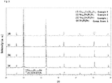
- the compound of Comparative Example 1 exhibits inferior phase stability when left at a relatively low temperature, and thus, the decomposition of the chalocogen-containing compound of Sn 4 Bi 2 Se 7 is generated, thus forming many secondary phases(Bi 3 Se 4 , Bi 8 Se 9 , Sn 3 Bi 9 Se 13 ) (The peaks resulting from the many secondary phases are confirmed in XRD pattern).
- the compounds of Examples 1 to 3 maintain face-centered cubic lattice structures without generation of secondary phases, and exhibit excellent phase stability.
- the compounds of Examples 1 to 3 exhibit excellent phase stability even at a relatively low temperature.
- Examples 1 to 3 generally exhibit excellent electrical conductivities, and particularly, it was confirmed that electrical conductivities is in the order of Example 2 > Example 1 > Example 3. It is expected that Example 2 with higher alkali metal content has excellent electric conductivity because the alkali metal is cationized and can donate electrons, and that Example 3 exhibits relatively low electric conductivity because the content of Bi that is cationized into Bi 3+ and can donate more electrons is low,
- Seebeck coefficients (S) were measured according to temperature change and are shown in FIG. 5b .
- the Seebeck coefficient was measured at a temperature range of 100 to 300 °C by differential voltage/temperature technique, using measuring equipment of LSR-3 from Linseis Inc.
- Examples 1 to 3 exhibit a positive or negative Seebeck coefficient that can be applied as thermoelectric conversion material.
- Example 1 if the content of Bi decreases and the content of an alkali metal increases, the alkali metal donates less electrons compared to the Bi decrease, thus exhibiting P-type material property like Example 1.
- Examples 1 to 3 generally exhibit excellent output factors, and among them, the specimen of Example 1 exhibits most excellent output factor. Particularly, the output factor measured at 100°C was about 3.62 ⁇ W/cmK 2 .
- thermal conductivities and lattice thermal conductivities were measured according to temperature change and are shown in FIG. 5d and FIG. 5e , respectively.
- Examples 1 to 3 generally exhibit low thermal conductivities and lattice thermal conductivities. Particularly, despite k E contributing to high electric conductivity, the specimen of Example 1 exhibits the lowest thermal conductivity because the lattice thermal conductivity is relatively the lowest as shown in Fig. 5e . The lattice thermal conductivity decreases as the concentration of the vacancy in the lattice increases, as shown in Table 2. Particularly, at 200°C, the specimen of Example 1 exhibited very low lattice thermal conductivity (0.51 W/mK).
- thermoelectric figures of merit were calculated according to temperature change and are shown in FIG. 5f .
Landscapes
- Chemical & Material Sciences (AREA)
- Organic Chemistry (AREA)
- Inorganic Chemistry (AREA)
- Engineering & Computer Science (AREA)
- Manufacturing & Machinery (AREA)
- Inorganic Compounds Of Heavy Metals (AREA)
- Powder Metallurgy (AREA)
Abstract
Description
- This application claims the benefit of Korean Patent Application No.
10-2016-0142891 filed on October 31, 2016 10-2017-0134204 filed on October 16, 2017 - The present invention relates to a novel chalcogen-containing compound that exhibits low thermal conductivity and excellent thermoelectric properties, and exhibits excellent phase stability even at relatively low temperature, a method for preparing the same, and a thermoelectric element including the same.
- Due to recent environmental problems caused by resource depletion and combustion, studies on thermoelectric conversion materials using waste heat are progressing as one of alternative energy sources.
- The energy conversion efficiency of such thermoelectric conversion material depends on a thermoelectric figure of merit (ZT). Here, ZT is determined according to the Seebeck coefficient, electrical conductivity, thermal conductivity, etc., and more specifically, it is proportional to the square of the Seebeck coefficient and electrical conductivity, and is inversely proportional to thermal conductivity. Thus, in order to increase the energy conversion efficiency of a thermoelectric element, the development of a thermoelectric conversion material having a high Seebeck coefficient or electrical conductivity or low thermal conductivity is required.
- Among the various thermoelectric conversion materials known before, thermoelectric conversion materials with a crystal lattice structure related to or similar to sodium chloride (NaCI), in which a part of the lattice site is vacant, such as PbTe, Bi2Te3, SnSe, etc., for example, are known to exhibit an excellent thermoelectric conversion property. That is, it is considered that materials having such a crystal lattice structure exhibit excellent electrical conductivity due to the crystal lattice structure similar to sodium chloride, and exhibit low thermal conductivity because a part of the lattice site becomes vacant. Thus, thermoelectric conversion materials having the above-described crystal lattice structure are known to have an excellent thermoelectric conversion property, and thus are being applied.
- Nevertheless, little is known about a thermoelectric conversion material that has face-centered cubic lattice structure identical to sodium chloride as shown in
FIG. 1 , in which a part of the lattice site is vacant. - However, Sn4Bi2Se7, one of Si-Bi-Se-based chalcogen compounds, is known to have an identical face-centered cubic lattice structure to that of sodium chloride, and includes a lattice site of which a part is vacant. For reference,
FIG. 2 shows a phase stability diagram of representative Sn-Bi-Se-based chalcogen compounds, wherein Sn4Bi2Se7 is known to have the face-centered cubic lattice structure at a temperature of about 580 to 720 °C (a part indicated by a circle inFIG. 2 ). - However, such chalcogen compounds maintain stability only at a temperature range of about 580 to 720 °C, and at lower temperature, particularly at the driving temperature of a thermoelectric element, they cannot exhibit phase stability because they are decomposed to other phases.
- Consequently, although it is expected that the above-described chalcogen compound exhibits low thermal conductivity and an excellent thermoelectric property because it has a face-centered cubic lattice structure including a lattice site of which a part is vacant, it exhibits inferior phase stability at a low temperature of about 580 °C or less, corresponding to the general driving temperature of thermoelectric elements, and thus application as a thermoelectric conversion material is very limited.
- The present invention provides a novel chalcogen-containing compound that exhibits low thermal conductivity and excellent thermoelectric properties, and exhibits excellent phase stability even at relatively low temperature, and a method for preparing the same.
- Further, the present invention provides a thermoelectric element including the chalcogen-containing compound.
- The present invention provides a chalcogen-containing compound represented by the following Chemical Formula 1:
[Chemical Formula 1] MxSnyBizSe7
- wherein, in Chemical Formula 1, M is an alkali metal,
- x, y and z are mole ratios of M, Sn, and Bi respectively, x is greater than 0 and equal to or less than 2, y is greater than 0 and equal to or less than 4, z is greater than 0 and equal to or less than 2, y+z is greater than 0 and equal to or less than 6, and x+y+z is greater than 0 and equal to or less than 7.
- The present invention also provides a method for preparing the chalcogen-containing compound, comprising the steps of:
- progressing a solid phase reaction of a mixture comprising raw materials comprising Sn, Bi and Se, and raw material comprising alkali metal(M);
- grinding the product of the solid phase reaction; and
- sintering the ground product.
- The present invention also provides a thermoelectric element comprising the chalcogen-containing compound as a thermoelectric conversion material.
- Hereinafter, a chalcogen-containing compound, a method for preparing the same, and a thermoelectric element including the same according to specific embodiments of the invention will be explained in detail.
- According to one embodiment of the present invention, a chalcogen-containing compound represented by the following Chemical Formula 1 is provided.
[Chemical Formula 1] MxSnyBizSe7
- wherein, in Chemical Formula 1, M is an alkali metal,
- x, y and z are mole ratios of M, Sn, and Bi respectively, x is greater than 0 and equal to or less than 2, y is greater than 0 and equal to or less than 4, z is greater than 0 and equal to or less than 2, y+z is greater than 0 and equal to or less than 6, and x+y+z is greater than 0 and equal to or less than 7.
- The chalcogen-containing compound of the one embodiment is a compound represented by Chemical Formula 1 in which an alkali metal is added to a chalcogen compound such Sn4Bi2Se7, and it has the same crystal lattice structure as Sn4Bi2Se7, that is, a crystal structure of a face-centered cubic lattice structure that is identical to that of sodium chloride.
- More specifically, in the compound of the one embodiment, it appears that a part of a vacancy excluding the sites filled with Se, Sn and Bi is filled with the alkali metal atom, in the face-centered cubic lattice structure. A vacancy remaining after filled with the alkali metal atom may be maintained as it is, and the value of 7-(x+y+z) may be defined as the mole ratio of the vacancy.
- As demonstrated in the examples described below, it was confirmed that the compound of the one embodiment can exhibit excellent electrical conductivity due to the crystal lattice structure of a face-centered cubic lattice structure and the addition of an alkali metal. This results from the crystal lattice structure, and simultaneously, is because the alkali metal becomes in the form of ions, thus donating additional electrons.
- Further, the compound of the one embodiment has the above-described specific crystal structure, but the alkali metal does not completely fill the vacant lattice site, and a part thereof remains, and thus, the compound has low thermal conductivity. Thus, the compound of the one embodiment exhibits excellent thermoelectric conversion property resulting from high electric conductivity and low thermal conductivity.
- Moreover, it was confirmed that since the chalcogen-containing compound of the one embodiment has an alkali metal added in the crystal lattice structure, it exhibits excellent phase stability even at a low temperature (for example, a temperature of about 580 °C or more) corresponding to the driving temperature of a thermoelectric element. Such excellent phase stability can be confirmed by the maintenance of an identical XRD pattern and an identical crystal structure without decomposition of the compound, even when the chalcogen-containing compound of the one embodiment is finally prepared and left in the form of a sintered body, as shown in
Fig. 2 . - Thus, the chalcogen-containing compound of one embodiment overcomes the problems of previously known Sn4Bi2Se7, etc. in terms of inferior phase stability, and exhibits excellent phase stability even at the general driving temperature of a thermoelectric element, and simultaneously, exhibits excellent electrical conductivity, low thermal conductivity and excellent thermoelectric conversion property due to the unique crystal lattice structure. Thus, the chalcogen-containing compound of one embodiment can be very preferably used as a thermoelectric conversion material in various fields and applications.
- Meanwhile, as explained above, in the face-centered cubic lattice structure of the chalcogen-containing compound of one embodiment, at least a part of the vacancy excluding the sites filled with Se, Sn, and Bi is filled with the alkali metal atom. More specifically, in such a face-centered cubic lattice structure, the Se fills the anion sites of the face-centered cubic lattice structure, the Sn and Bi fill the cation sites of the face-centered cubic lattice structure, and the alkali metal(M) fills a part of a vacancy of the cation sites remaining after filled with Sn and Bi.
- Herein, the alkali metal, and Sn and Bi that fill each cation site become cations, and can donate electrons, thus contributing to the excellent electrical conductivity of the compound of one embodiment. In addition, since the addition of the alkali metal may contribute to excellent phase stability, and the alkali metal cannot completely fill the vacant lattice site and a vacancy remains, the chalcogen-containing compound of one embodiment may exhibit low thermal conductivity.
- As the alkali metal, one or more alkali metals selected from the group consisting of Na, and K may be used, but considering high electrical conductivity and excellent phase stability of the compound of one embodiment, Na may be appropriately used.
- And, in the
Chemical Formula 1, x, y and z denote mole ratios of M, Sn, and Bi respectively, wherein x is greater than 0 and equal to or less than 2 (or greater than 0 and less than 2), y is greater than 0 and equal to or less than 4, z is greater than 0 and equal to or less than 2, y+z is greater than 0 and equal to or less than 6, and x+y+z is greater than 0 and equal to or less than 7. More specifically, x may be 0.05 to 0.8, or 0.1 to 0.5, or 0.2 to 0.4, y may be 3.5 to 4, or 3.7 to 4, or 3.9 to 4, z may be 1.5 to 2, or 1.7 to 2, or 1.9 to 2. And, y+z may be 5 to 6, or 5.4 to 6, or 5.8 to 6, and x+y+z may be 5 to 6.8, or 6.1 to 6.8, or 6.2 to 6.8. - As explained above, the value of 7-(x+y+z) may be defined as the mole ratio of a vacancy remaining after filled with the above explained atoms, and it may be greater than 0, or greater than 0 and equal to or less than 0.2.
- By fulfilling each mole ratio, the compound of one embodiment can maintain the unique crystal lattice structure, and yet, exhibit excellent phase stability due to the addition of an alkali metal, and exhibit low thermal conductivity because the alkali metal does not excessively fills the vacant lattice sites. Also, since the mole ratios of the alkali metal, Bi, etc. that donate electrons are optimized, the compound of one embodiment can exhibit more excellent electrical conductivity.
- Since the chalcogen-containing compound of the above-explained one embodiment has low thermal conductivity, high electrical conductivity, and the resulting excellent thermoelectric conversion property, and high phase stability, it can be preferably used as a thermoelectric conversion material in various thermoelectric cooling systems, thermoelectric generation systems, etc.
- Meanwhile, according to another embodiment of the present invention, a method for preparing the above-explained chalcogen-containing compound is provided. The preparation method includes the steps of: progressing a solid phase reaction of a mixture comprising raw materials comprising Sn, Bi and Se, and raw material comprising alkali metal(M); grinding the product of the solid phase reaction; and sintering the ground product.
- In the preparation method, as the raw material comprising Sn, Bi and Se, for example, each powder of Sn, Bi and Se may be used, and as the raw material comprising alkali metal, although specifically limited, M2Se(M is an alkali metal) powder may be used.
- And, each raw material may be mixed at a ratio corresponding to the mole ratio(x, y, z 7) of the
Chemical Formula 1. For example, in case each Sn, Bi and Se powder and M2Se powder are used as raw materials, each raw material of M2Se, Sn, Bi and Se may be mixed at a mole ratio of x/2 : y: z : 7-x, considering that Se is also included in the raw material of M2Se. - The formation of the mixture of raw materials may be performed by adding each raw material at predetermined rates, then grinding or milling, and selectively pelletizing. The formed mixture may be in the state of a powder, pellet, ingot, etc. according to the process.
- A solid phase state reaction step for such a mixture may be progressed. Such a solid phase reaction step may be conducted by various intermetallic reaction processes known before, and for example, it may be progressed at a temperature of 500 to 700°C for each powder raw material. Heat treatment for such a solid phase reaction may be progressed in a furnace such as an electric furnace, etc., and it may be progressed under vacuum or inert gas atmosphere.
- And, although the heat treatment and solid phase reaction may be progressed in a single step, they may be divided into two or more steps and progressed.
- After the solid phase reaction, the reaction product is ground. Such a grinding step may be performed using a previously known method and apparatus for preparing a thermoelectric conversion material, and through the grinding step, a powder product may be obtained.
- Meanwhile, between the solid phase reaction step and the grinding step, a step of cooling the product of the solid phase reaction step to form an ingot may be further performed. Here, the cooling may be performed using various cooling media, and any cooling devices and methods previously used in the preparation process of a thermoelectric conversion material may be used without specific limitations. After forming an ingot through the cooling step, the ingot may be ground.
- After the grinding step, the ground product may be sintered. By performing the sintering step, a chalcogen-containing compound in the form of a sintered body may be prepared.
- Such a sintering step may be performed by spark plasma sintering, etc. that are well known to a person having ordinary knowledge, and for example, it may be performed at a temperature of 550 °C or more and a pressure of 10 MPa or more. According to a more specific embodiment, the sintering step may be performed at a temperature of 550 to 700 °C and a pressure of 10 to 100 MPa for 5 to 10 minutes.
- After performing the sintering, a cooling step may be further performed.
- Since the above-explained steps may be performed by applying common preparation conditions, methods, and apparatuses for forming a metal compound such as a chalcogen compound or thermoelectric conversion material, and specific reaction conditions and methods are described in the examples below, additional explanations thereof are omitted.
- According to yet another embodiment of the present invention, a thermoelectric element including the chalcogen-containing compound of the above embodiment as a thermoelectric conversion material is provided. Such a thermoelectric element may include the chalcogen-containing compound of the above embodiment (thermoelectric conversion material) as a p-type or n-type thermoelectric conversion material, and for this, it may include a compound additionally doped with an additional p-type or n-type element as a thermoelectric conversion material. The kind of the p-type element or n-type element or doping method that can be used is not specifically limited, and elements and doping methods commonly used to apply a thermoelectric conversion material as a p-type or n-type before may be used.
- The thermoelectric element may include a thermoelectric element formed by processing and molding a p-type or n-type thermoelectric conversion material obtained in the form of a sintered body, and it may include an insulation substrate and electrode For the combination structure of the thermoelectric element, insulation substrate, and electrode, the structure of a common thermoelectric element may be applied.
- As the insulation substrate, a sapphire substrate, a silicon substrate, a Pyrex substrate, a quartz substrate, etc. may be used, and as the electrode, any electrodes including metals or conductive metal compounds may be used.
- Since the above-explained thermoelectric element includes the thermoelectric conversion material of one embodiment, it may exhibit an excellent thermoelectric conversion property, and may be preferably applied as a thermoelectric cooling system, thermoelectric generation system, etc. in various fields and uses.
- According to the present invention, a novel chalcogen-containing compound that exhibits low thermal conductivity and excellent thermoelectric properties, and exhibits excellent phase stability even at relatively low temperature, and a method for preparing the same can be provided. By applying such a chalcogen-containing compound, a thermoelectric element exhibiting excellent properties can be provided.
-
-
FIG. 1 is a schematic diagram showing the face-centered cubic lattice structure that is exhibited by sodium chloride, etc. -
FIG. 2 is a phase stability diagram of representative Sn-Bi-Se-based chalcogen compounds. -
FIG. 3 is a graph showing X-ray diffraction analysis results of a chalcogen compound powder immediately before passing through a sintering process in Examples 1 to 3 and Comparative Example 1. -
FIG. 4 is a graph showing X-ray diffraction analysis results of the sintered bodies finally prepared through a sintering process, after slow cooling and leaving at room temperature, in Examples 1 to 3 and Comparative Example 1. -
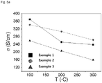
FIG. 5a is a graph showing results of measuring electrical conductivities of chalcogen compounds of Examples 1 to 3 according to temperature. -
FIG. 5b is a graph showing results of measuring Seebeck coefficients of the chalcogen compounds of Examples 1 to 3 according to temperature. -
FIG. 5c is a graph showing results of measuring output factors of the chalcogen compounds of Examples 1 to 3 according to temperature. -
FIG. 5d is a graph showing results of measuring thermal conductivities of the chalcogen compounds of Examples 1 to 3 according to temperature. -
FIG. 5e is a graph showing results of measuring lattice thermal conductivities of the chalcogen compounds of Examples 1 to 3 according to temperature. -
FIG. 5f is a graph showing results of measuring thermoelectric figures of merit of the chalcogen compounds of Examples 1 to 3 according to temperature. - The present invention will be explained in more detail in the following examples. However, these examples are presented only as illustrations of the present invention, and the scope of the present invention is not limited thereby.
- Each powder of high purity raw materials of Sn, Bi, Se and Na2Se was weighed in a glove box at a mole ratio of 4 : 2 : 6.9 (7-0.1) : 0.1, put in a carbon crucible, and then charged into a quartz tube. The inside of the quartz tube was evacuated and sealed. The raw materials were maintained at a constant temperature in an electric furnace at 620 °C for 24 hours.
- Thereafter, the quartz tube in which a reaction was performed was cooled with water to obtain an ingot, the ingot was finely ground to powder with a particle diameter of 75 µm or less, and sintered by spark plasma sintering (SPS) at a temperature of 620 °C and a pressure of 50 MPa for 10 minutes, thus preparing a chalcogen-containing compound of Na0.2Sn4Bi2Se7.
- A chalcogen-containing compound of Na0.4Sn4Bi2Se7 was prepared by the same method as Example 1, except that each powder of high purity raw materials of Sn, Bi, Se and Na2Se was mixed in a glove box at a mole ratio of 4 : 2 : 6.8 (7-0.2) : 0.2.
- A chalcogen-containing compound of Na0.75Sn4Bi1.7Se7 was prepared by the same method as Example 1, except that each powder of high purity raw materials of Sn, Bi, Se and Na2Se was mixed in a glove box at a mole ratio of 4 : 1.7 : 6.625 (7-0.375) : 0.375.
- A chalcogen-containing compound of Sn4Bi2Se7 was prepared by the same method as Example 1, except that each powder of high purity raw materials of Sn, Bi and Se was mixed in a glove box at a mole ratio of 4 : 2 : 7.
- For the powder chalcogen-containing compounds immediately before the sintering process in Examples 1 to 3 and Comparative Example 1, X-ray diffraction analysis was performed and the results are shown in
FIG. 3 . And, the sintered bodies finally prepared through the sintering processes in Examples 1 to 3 and Comparative Example 1 were slowly cooled from about 620 °C to 300 °C, and then cooled again to room temperature (25°C), and the sintered bodies were maintained under an air atmosphere for 15 days, and then each sintered body was subjected to X-ray diffraction analysis, and the results are shown inFIG. 4 . - And, using the TOPAS program, the lattice parameter of each powder chalcogen-containing compound of Examples 1 to 3 and Comparative Example 1 was calculated and is shown in the following Table 1.
[Table 1] Powder material Lattice parameter (Å) Example 1 5.9523 Example 2 5.9665 Example 3 5.9642 Comparative Example 5.9448 - In addition, for the powder chalcogen-containing compounds of Examples 1 to 3 and Comparative Example 1, the number of atoms for each component in the unit lattice is shown in the following Table 2.
[Table 2] Powder material Number of atoms for each component in unit lattice Sn Bi Se Vacancy Na Example1 2.2853 1.1426 4 0.458 0.114 Example12 2.2853 1.1426 4 0.344 0.228 Example13 2.2853 1 4 0.286 0.4287 Com parative Example1 2.2853 1.1426 4 0.572 0 - First, referring to
FIG. 3 , it was confirmed that all the powder chalcogen-containing compounds of Examples 1 to 3 have crystal lattice structures identical to the chalcogen-containing compound of Comparative Example 1 (i.e., Sn4Bi2Se7 which was previously known to have a face-centered cubic lattice structure at a high temperature), and thusm it was confirmed that all the compounds of Examples 1 to 3 have a crystal lattice structure of a face-centered cubic lattice structure. - And, referring to Table 1, in Examples 1 to 3, with the addition of alkali metal(Na), a lattice parameter increased compared to Comparative Example 1, and thus, it is inferred that the alkali metal fills a vacancy of the crystal lattice structure. Particularly, comparison of Examples 1 and 2 shows that a lattice parameter increases as the content of alkali metal increases, but Example 3 with relatively small Bi rate exhibits deceased lattice parameter compared to Example 2, and thus, it is confirmed that the alkali metal fills a vacancy of the crystal lattice structure, but since the atomic radius of the alkali metal(Na) is smaller than that of Bi, Example 3 exhibits decreased lattice parameter.
- And, referring to Table 2, it is expected that in Examples 1 to 3 including an alkali metal, the concentration of the vacancy of the lattice structure decreases compared to Comparative Example 1, and that in Examples 1 and 2, the concentration of electrons increases due to electron donation by the alkali metal. Meanwhile, it is expected that in the case of Example 3 with decreased Bi content, the concentration of electrons decreases (the concentration of holes increases) because Na+ donates two less electrons compared to Bi3+.
- Referring to
FIG. 4 , it is confirmed that the compound of Comparative Example 1 exhibits inferior phase stability when left at a relatively low temperature, and thus, the decomposition of the chalocogen-containing compound of Sn4Bi2Se7is generated, thus forming many secondary phases(Bi3Se4, Bi8Se9, Sn3Bi9Se13) (The peaks resulting from the many secondary phases are confirmed in XRD pattern). To the contrary, it is confirmed that the compounds of Examples 1 to 3 maintain face-centered cubic lattice structures without generation of secondary phases, and exhibit excellent phase stability. Thus, it is confirmed that the compounds of Examples 1 to 3 exhibit excellent phase stability even at a relatively low temperature.
- For the chalcogen-containing compound specimens prepared in Examples 1 to 3, electrical conductivities were measured according to temperature change and are shown in
FIG. 5a . The electrical conductivity was measured at a temperature range of 100 to 300 °C through a four-probe direct current method, using a resistivity meter of LSR-3 from Linseis Inc. - Referring to
FIG. 5a , it was confirmed that Examples 1 to 3 generally exhibit excellent electrical conductivities, and particularly, it was confirmed that electrical conductivities is in the order of Example 2 > Example 1 > Example 3. It is expected that Example 2 with higher alkali metal content has excellent electric conductivity because the alkali metal is cationized and can donate electrons, and that Example 3 exhibits relatively low electric conductivity because the content of Bi that is cationized into Bi3+ and can donate more electrons is low, - For the chalcogen-containing compound specimens prepared in Examples 1 to 3, Seebeck coefficients (S) were measured according to temperature change and are shown in
FIG. 5b . The Seebeck coefficient was measured at a temperature range of 100 to 300 °C by differential voltage/temperature technique, using measuring equipment of LSR-3 from Linseis Inc. - As shown in
Fig. 5b , it is confirmed that Examples 1 to 3 exhibit a positive or negative Seebeck coefficient that can be applied as thermoelectric conversion material. - However, comparing Examples 1 and 2, it is confirmed that as the content of an alkali metal increases from 0.2 to 0.4, the Seebeck coefficient changes from a positive(+) to a negative(-) value. It means that the main charge carrier of material is changed from holes to electrons due to the additional electron donation by the alkali metal, and indicates property change from P-type to N-type semiconductor material. It means that the main charge carrier in Example 1 is hole despite the additional electron donation by the alkali metal. As in Example 3, if the content of Bi decreases and the content of an alkali metal increases, the alkali metal donates less electrons compared to the Bi decrease, thus exhibiting P-type material property like Example 1.
- For the chalcogen-containing compound specimens prepared in Examples 1 to 3, output factors were calculated according to temperature change and are shown in
FIG. 5c . - The output factor is defined as power factor (PF) = σS2, and it was calculated using the values of σ (electrical conductivity) and S (Seebeck coefficient) shown in
FIGS. 5a and5b . - As shown in
FIG. 5c , it was confirmed that Examples 1 to 3 generally exhibit excellent output factors, and among them, the specimen of Example 1 exhibits most excellent output factor. Particularly, the output factor measured at 100°C was about 3.62 µ W/cmK2. - For the chalcogen-containing compound specimens prepared in Examples 1 to 3, thermal conductivities and lattice thermal conductivities were measured according to temperature change and are shown in
FIG. 5d andFIG. 5e , respectively. For the measurement of thermal conductivity, first, thermal diffusivity (D) and heat capacity (Cp) were measured by a laser flash method, using thermal conductivity measuring equipment of LFA457 from Netzsch Company. The measured values were applied in the equation "thermal conductivity (k) = DρCp (ρ is the density of a sample measured by Archimedes' principle)". - Further, total thermal conductivity (k= kL + kE) is divided into lattice thermal conductivity (kL) and thermal conductivity (kE) calculated according to Wiedemann-Franz law (kE = LσT), wherein, as the Lorentz number (L), a value calculated from the Seebeck coefficient according to temperature was used.
- Referring to
FIGS. 5d and5e , Examples 1 to 3 generally exhibit low thermal conductivities and lattice thermal conductivities. Particularly, despite kE contributing to high electric conductivity, the specimen of Example 1 exhibits the lowest thermal conductivity because the lattice thermal conductivity is relatively the lowest as shown inFig. 5e . The lattice thermal conductivity decreases as the concentration of the vacancy in the lattice increases, as shown in Table 2. Particularly, at 200°C, the specimen of Example 1 exhibited very low lattice thermal conductivity (0.51 W/mK). - For the chalcogen-containing compound specimens prepared in Examples 1 to 3, the thermoelectric figures of merit were calculated according to temperature change and are shown in
FIG. 5f . The thermoelectric figure of merit is defined as ZT=S2σT/k, and it was calculated using the S (Seebeck coefficient), σ (electrical conductivity), T (absolute temperature), and k (thermal conductivity) values obtained in experimental examples. - Referring to
FIG. 5f , it was confirmed that Examples 1 to 3 exhibit excellent thermoelectric figures of merit that can be applied as a thermoelectric conversion material. Specifically, as the temperature rises, the ZT value increased until 200°C, and thereafter, tended to decrease. The specimen of Example 1 exhibited most excellent thermoelectric figure of merit(ZT=0.24) at 200 °C.
Claims (13)
- A chalcogen-containing compound represented by the following Chemical Formula 1:
[Chemical Formula 1] MxSnyBizSe7
wherein, in Chemical Formula 1, M is an alkali metal,x, y and z are mole ratios of M, Sn, and Bi respectively, x is greater than 0 and equal to or less than 2, y is greater than 0 and equal to or less than 4, z is greater than 0 and equal to or less than 2, y+z is greater than 0 and equal to or less than 6, and x+y+z is greater than 0 and equal to or less than 7. - The chalcogen-containing compound according to claim 1, wherein M is one or more alkali metals selected from the group consisting of Na, and K.
- The chalcogen-containing compound according to claim 1, wherein the compound has a crystal structure of a face-centered cubic lattice structure.
- The chalcogen-containing compound according to claim 3, wherein M fills a part of a vacancy excluding the sites filled with Se, Sn and Bi in the face-centered cubic lattice structure.
- The chalcogen-containing compound according to claim 3, wherein
the Se fills the anion sites of the face-centered cubic lattice structure, the Sn and Bi fill the cation sites of the face-centered cubic lattice structure, and
the M fills a part of a vacancy of the remaining cation site, excluding the sites filled with Sn and Bi. - The chalcogen-containing compound according to claim 1, wherein the compound is used as thermoelectric conversion material.
- A method for preparing the chalcogen-containing compound of claim 1, comprising the steps of:progressing a solid phase reaction of a mixture comprising raw materials comprising Sn, Bi and Se, and raw material comprising alkali metal(M);grinding the product of the solid phase reaction; andsintering the ground product.
- The method for preparing a chalcogen-containing compound according to claim 7, wherein the raw material comprising alkali metal comprises M2Se(M is alkali metal) powder.
- The method for preparing a chalcogen-containing compound according to claim 7, wherein the solid phase reaction is performed at a temperature of 500 to 700°C, for each powder raw material.
- The method for preparing a chalcogen-containing compound according to claim 7, further comprising a step of cooling the product of the solid phase reaction to form an ingot, between the solid phase reaction step and the grinding step.
- The method for preparing a chalcogen-containing compound according to claim 7, wherein the sintering step is performed by a spark plasma sintering method.
- The method for preparing a chalcogen-containing compound according to claim 7, wherein the sintering step is performed at a temperature of 550 °C or more and a pressure of 10MPa or more.
- A thermoelectric element comprising the chalcogen-containing compound according to any one of claims 1 to 5, as a thermoelectric conversion material.
Applications Claiming Priority (3)
| Application Number | Priority Date | Filing Date | Title |
|---|---|---|---|
| KR20160142891 | 2016-10-31 | ||
| KR1020170134204A KR102094451B1 (en) | 2016-10-31 | 2017-10-16 | Chalcogen-containing compound, its preparation method and thermoelectric element comprising the same |
| PCT/KR2017/011479 WO2018080085A1 (en) | 2016-10-31 | 2017-10-17 | Chalcogenide compound, production method thereof and thermoelectric element comprising same |
Publications (3)
| Publication Number | Publication Date |
|---|---|
| EP3470374A1 true EP3470374A1 (en) | 2019-04-17 |
| EP3470374A4 EP3470374A4 (en) | 2019-06-19 |
| EP3470374B1 EP3470374B1 (en) | 2020-04-01 |
Family
ID=62184351
Family Applications (1)
| Application Number | Title | Priority Date | Filing Date |
|---|---|---|---|
| EP17865873.8A Active EP3470374B1 (en) | 2016-10-31 | 2017-10-17 | Chalcogenide compound, production method thereof and thermoelectric element comprising same |
Country Status (5)
| Country | Link |
|---|---|
| US (1) | US11276809B2 (en) |
| EP (1) | EP3470374B1 (en) |
| JP (1) | JP6833249B2 (en) |
| KR (1) | KR102094451B1 (en) |
| CN (1) | CN109476502B (en) |
Families Citing this family (4)
| Publication number | Priority date | Publication date | Assignee | Title |
|---|---|---|---|---|
| KR102121434B1 (en) * | 2017-05-15 | 2020-06-10 | 주식회사 엘지화학 | Chalcogen-containing compound, its preparation method and thermoelectric element comprising the same |
| KR102123041B1 (en) | 2017-06-07 | 2020-06-15 | 주식회사 엘지화학 | Chalcogen-containing compound, its preparation method and thermoelectric element comprising the same |
| KR102121436B1 (en) | 2017-06-27 | 2020-06-10 | 주식회사 엘지화학 | Chalcogen-containing compound, its preparation method and thermoelectric element comprising the same |
| US11358864B2 (en) | 2017-06-30 | 2022-06-14 | Lg Chem, Ltd. | Chalcogen-containing compound, its preparation method and thermoelectric element comprising the same |
Family Cites Families (10)
| Publication number | Priority date | Publication date | Assignee | Title |
|---|---|---|---|---|
| US6013204A (en) | 1997-03-28 | 2000-01-11 | Board Of Trustees Operating Michigan State University | Alkali metal chalcogenides of bismuth alone or with antimony |
| US6312617B1 (en) * | 1998-10-13 | 2001-11-06 | Board Of Trustees Operating Michigan State University | Conductive isostructural compounds |
| KR101688529B1 (en) * | 2009-01-06 | 2016-12-22 | 삼성전자주식회사 | Thermoelectric materials, and thermoelectric module and thermoelectric apparatus comprising same |
| KR101172802B1 (en) | 2009-12-31 | 2012-08-09 | 한국전기연구원 | fabrication method for Te-based thermoelectric materials containing twins formed by addition of dopant and thermoelectric materials thereby |
| KR101680763B1 (en) | 2010-03-31 | 2016-11-29 | 삼성전자주식회사 | Thermoelectric materials, and thermoelectric module and thermoelectric device comprising same |
| US8685779B1 (en) * | 2012-11-10 | 2014-04-01 | Sharp Laboratories Of America, Inc. | Group VA-doped solution-processed metal chalcogenides |
| KR102122553B1 (en) * | 2013-03-25 | 2020-06-12 | 에스케이이노베이션 주식회사 | Natural superlattice structured thermoelectric materials |
| JP6164627B2 (en) | 2013-10-04 | 2017-07-19 | エルジー・ケム・リミテッド | New compound semiconductors and their utilization |
| CN104261357B (en) | 2014-09-23 | 2016-06-15 | 清华大学 | A kind of Bi2O2Se base thermoelectricity material and preparation method thereof |
| KR101679960B1 (en) | 2015-04-07 | 2016-11-28 | 공주대학교 산학협력단 | Fabrication method for Bi2Te3 thermoelectric materials |
-
2017
- 2017-10-16 KR KR1020170134204A patent/KR102094451B1/en active Active
- 2017-10-17 EP EP17865873.8A patent/EP3470374B1/en active Active
- 2017-10-17 JP JP2019524009A patent/JP6833249B2/en active Active
- 2017-10-17 CN CN201780043189.4A patent/CN109476502B/en active Active
- 2017-10-17 US US16/312,842 patent/US11276809B2/en active Active
Also Published As
| Publication number | Publication date |
|---|---|
| EP3470374B1 (en) | 2020-04-01 |
| KR102094451B1 (en) | 2020-03-27 |
| CN109476502A (en) | 2019-03-15 |
| JP2019528235A (en) | 2019-10-10 |
| EP3470374A4 (en) | 2019-06-19 |
| KR20180048313A (en) | 2018-05-10 |
| US11276809B2 (en) | 2022-03-15 |
| US20190288172A1 (en) | 2019-09-19 |
| JP6833249B2 (en) | 2021-02-24 |
| CN109476502B (en) | 2021-05-18 |
Similar Documents
| Publication | Publication Date | Title |
|---|---|---|
| EP3470374B1 (en) | Chalcogenide compound, production method thereof and thermoelectric element comprising same | |
| US11309476B2 (en) | Chalcogen-containing compound, its preparation method and thermoelectric element comprising the same | |
| CN110088924B (en) | Chalcogen-containing compound, method for producing the same, and thermoelectric element comprising the same | |
| CN110268107B (en) | Chalcogen-containing compound, method for producing the same, and thermoelectric element comprising the same | |
| US11245062B2 (en) | Chalcogen-containing compound, its preparation method and thermoelectric element comprising the same | |
| WO2018080085A1 (en) | Chalcogenide compound, production method thereof and thermoelectric element comprising same | |
| JP6821235B2 (en) | Chalcogen compounds, their production methods, and thermoelectric devices containing them | |
| JP6755566B2 (en) | Chalcogen compounds, their production methods, and thermoelectric devices containing them |
Legal Events
| Date | Code | Title | Description |
|---|---|---|---|
| STAA | Information on the status of an ep patent application or granted ep patent |
Free format text: STATUS: THE INTERNATIONAL PUBLICATION HAS BEEN MADE |
|
| PUAI | Public reference made under article 153(3) epc to a published international application that has entered the european phase |
Free format text: ORIGINAL CODE: 0009012 |
|
| STAA | Information on the status of an ep patent application or granted ep patent |
Free format text: STATUS: REQUEST FOR EXAMINATION WAS MADE |
|
| 17P | Request for examination filed |
Effective date: 20190109 |
|
| AK | Designated contracting states |
Kind code of ref document: A1 Designated state(s): AL AT BE BG CH CY CZ DE DK EE ES FI FR GB GR HR HU IE IS IT LI LT LU LV MC MK MT NL NO PL PT RO RS SE SI SK SM TR |
|
| AX | Request for extension of the european patent |
Extension state: BA ME |
|
| REG | Reference to a national code |
Ref country code: DE Ref legal event code: R079 Ref document number: 602017014155 Country of ref document: DE Free format text: PREVIOUS MAIN CLASS: C01G0029000000 Ipc: H01L0035160000 |
|
| A4 | Supplementary search report drawn up and despatched |
Effective date: 20190520 |
|
| RIC1 | Information provided on ipc code assigned before grant |
Ipc: H01L 35/16 20060101AFI20190514BHEP Ipc: C01B 19/00 20060101ALI20190514BHEP Ipc: C01G 29/00 20060101ALI20190514BHEP |
|
| GRAP | Despatch of communication of intention to grant a patent |
Free format text: ORIGINAL CODE: EPIDOSNIGR1 |
|
| STAA | Information on the status of an ep patent application or granted ep patent |
Free format text: STATUS: GRANT OF PATENT IS INTENDED |
|
| DAV | Request for validation of the european patent (deleted) | ||
| DAX | Request for extension of the european patent (deleted) | ||
| INTG | Intention to grant announced |
Effective date: 20191115 |
|
| GRAS | Grant fee paid |
Free format text: ORIGINAL CODE: EPIDOSNIGR3 |
|
| GRAA | (expected) grant |
Free format text: ORIGINAL CODE: 0009210 |
|
| STAA | Information on the status of an ep patent application or granted ep patent |
Free format text: STATUS: THE PATENT HAS BEEN GRANTED |
|
| AK | Designated contracting states |
Kind code of ref document: B1 Designated state(s): AL AT BE BG CH CY CZ DE DK EE ES FI FR GB GR HR HU IE IS IT LI LT LU LV MC MK MT NL NO PL PT RO RS SE SI SK SM TR |
|
| REG | Reference to a national code |
Ref country code: GB Ref legal event code: FG4D |
|
| REG | Reference to a national code |
Ref country code: CH Ref legal event code: EP Ref country code: AT Ref legal event code: REF Ref document number: 1252509 Country of ref document: AT Kind code of ref document: T Effective date: 20200415 |
|
| REG | Reference to a national code |
Ref country code: DE Ref legal event code: R096 Ref document number: 602017014155 Country of ref document: DE |
|
| REG | Reference to a national code |
Ref country code: IE Ref legal event code: FG4D |
|
| PG25 | Lapsed in a contracting state [announced via postgrant information from national office to epo] |
Ref country code: BG Free format text: LAPSE BECAUSE OF FAILURE TO SUBMIT A TRANSLATION OF THE DESCRIPTION OR TO PAY THE FEE WITHIN THE PRESCRIBED TIME-LIMIT Effective date: 20200701 |
|
| REG | Reference to a national code |
Ref country code: NL Ref legal event code: MP Effective date: 20200401 |
|
| REG | Reference to a national code |
Ref country code: LT Ref legal event code: MG4D |
|
| PG25 | Lapsed in a contracting state [announced via postgrant information from national office to epo] |
Ref country code: GR Free format text: LAPSE BECAUSE OF FAILURE TO SUBMIT A TRANSLATION OF THE DESCRIPTION OR TO PAY THE FEE WITHIN THE PRESCRIBED TIME-LIMIT Effective date: 20200702 Ref country code: FI Free format text: LAPSE BECAUSE OF FAILURE TO SUBMIT A TRANSLATION OF THE DESCRIPTION OR TO PAY THE FEE WITHIN THE PRESCRIBED TIME-LIMIT Effective date: 20200401 Ref country code: PT Free format text: LAPSE BECAUSE OF FAILURE TO SUBMIT A TRANSLATION OF THE DESCRIPTION OR TO PAY THE FEE WITHIN THE PRESCRIBED TIME-LIMIT Effective date: 20200817 Ref country code: LT Free format text: LAPSE BECAUSE OF FAILURE TO SUBMIT A TRANSLATION OF THE DESCRIPTION OR TO PAY THE FEE WITHIN THE PRESCRIBED TIME-LIMIT Effective date: 20200401 Ref country code: IS Free format text: LAPSE BECAUSE OF FAILURE TO SUBMIT A TRANSLATION OF THE DESCRIPTION OR TO PAY THE FEE WITHIN THE PRESCRIBED TIME-LIMIT Effective date: 20200801 Ref country code: SE Free format text: LAPSE BECAUSE OF FAILURE TO SUBMIT A TRANSLATION OF THE DESCRIPTION OR TO PAY THE FEE WITHIN THE PRESCRIBED TIME-LIMIT Effective date: 20200401 Ref country code: NO Free format text: LAPSE BECAUSE OF FAILURE TO SUBMIT A TRANSLATION OF THE DESCRIPTION OR TO PAY THE FEE WITHIN THE PRESCRIBED TIME-LIMIT Effective date: 20200701 Ref country code: NL Free format text: LAPSE BECAUSE OF FAILURE TO SUBMIT A TRANSLATION OF THE DESCRIPTION OR TO PAY THE FEE WITHIN THE PRESCRIBED TIME-LIMIT Effective date: 20200401 Ref country code: CZ Free format text: LAPSE BECAUSE OF FAILURE TO SUBMIT A TRANSLATION OF THE DESCRIPTION OR TO PAY THE FEE WITHIN THE PRESCRIBED TIME-LIMIT Effective date: 20200401 |
|
| REG | Reference to a national code |
Ref country code: AT Ref legal event code: MK05 Ref document number: 1252509 Country of ref document: AT Kind code of ref document: T Effective date: 20200401 |
|
| PG25 | Lapsed in a contracting state [announced via postgrant information from national office to epo] |
Ref country code: HR Free format text: LAPSE BECAUSE OF FAILURE TO SUBMIT A TRANSLATION OF THE DESCRIPTION OR TO PAY THE FEE WITHIN THE PRESCRIBED TIME-LIMIT Effective date: 20200401 Ref country code: RS Free format text: LAPSE BECAUSE OF FAILURE TO SUBMIT A TRANSLATION OF THE DESCRIPTION OR TO PAY THE FEE WITHIN THE PRESCRIBED TIME-LIMIT Effective date: 20200401 Ref country code: LV Free format text: LAPSE BECAUSE OF FAILURE TO SUBMIT A TRANSLATION OF THE DESCRIPTION OR TO PAY THE FEE WITHIN THE PRESCRIBED TIME-LIMIT Effective date: 20200401 |
|
| PG25 | Lapsed in a contracting state [announced via postgrant information from national office to epo] |
Ref country code: AL Free format text: LAPSE BECAUSE OF FAILURE TO SUBMIT A TRANSLATION OF THE DESCRIPTION OR TO PAY THE FEE WITHIN THE PRESCRIBED TIME-LIMIT Effective date: 20200401 |
|
| REG | Reference to a national code |
Ref country code: DE Ref legal event code: R097 Ref document number: 602017014155 Country of ref document: DE |
|
| PG25 | Lapsed in a contracting state [announced via postgrant information from national office to epo] |
Ref country code: ES Free format text: LAPSE BECAUSE OF FAILURE TO SUBMIT A TRANSLATION OF THE DESCRIPTION OR TO PAY THE FEE WITHIN THE PRESCRIBED TIME-LIMIT Effective date: 20200401 Ref country code: DK Free format text: LAPSE BECAUSE OF FAILURE TO SUBMIT A TRANSLATION OF THE DESCRIPTION OR TO PAY THE FEE WITHIN THE PRESCRIBED TIME-LIMIT Effective date: 20200401 Ref country code: EE Free format text: LAPSE BECAUSE OF FAILURE TO SUBMIT A TRANSLATION OF THE DESCRIPTION OR TO PAY THE FEE WITHIN THE PRESCRIBED TIME-LIMIT Effective date: 20200401 Ref country code: SM Free format text: LAPSE BECAUSE OF FAILURE TO SUBMIT A TRANSLATION OF THE DESCRIPTION OR TO PAY THE FEE WITHIN THE PRESCRIBED TIME-LIMIT Effective date: 20200401 Ref country code: IT Free format text: LAPSE BECAUSE OF FAILURE TO SUBMIT A TRANSLATION OF THE DESCRIPTION OR TO PAY THE FEE WITHIN THE PRESCRIBED TIME-LIMIT Effective date: 20200401 Ref country code: AT Free format text: LAPSE BECAUSE OF FAILURE TO SUBMIT A TRANSLATION OF THE DESCRIPTION OR TO PAY THE FEE WITHIN THE PRESCRIBED TIME-LIMIT Effective date: 20200401 Ref country code: RO Free format text: LAPSE BECAUSE OF FAILURE TO SUBMIT A TRANSLATION OF THE DESCRIPTION OR TO PAY THE FEE WITHIN THE PRESCRIBED TIME-LIMIT Effective date: 20200401 |
|
| PLBE | No opposition filed within time limit |
Free format text: ORIGINAL CODE: 0009261 |
|
| STAA | Information on the status of an ep patent application or granted ep patent |
Free format text: STATUS: NO OPPOSITION FILED WITHIN TIME LIMIT |
|
| PG25 | Lapsed in a contracting state [announced via postgrant information from national office to epo] |
Ref country code: PL Free format text: LAPSE BECAUSE OF FAILURE TO SUBMIT A TRANSLATION OF THE DESCRIPTION OR TO PAY THE FEE WITHIN THE PRESCRIBED TIME-LIMIT Effective date: 20200401 Ref country code: SK Free format text: LAPSE BECAUSE OF FAILURE TO SUBMIT A TRANSLATION OF THE DESCRIPTION OR TO PAY THE FEE WITHIN THE PRESCRIBED TIME-LIMIT Effective date: 20200401 |
|
| 26N | No opposition filed |
Effective date: 20210112 |
|
| PG25 | Lapsed in a contracting state [announced via postgrant information from national office to epo] |
Ref country code: SI Free format text: LAPSE BECAUSE OF FAILURE TO SUBMIT A TRANSLATION OF THE DESCRIPTION OR TO PAY THE FEE WITHIN THE PRESCRIBED TIME-LIMIT Effective date: 20200401 |
|
| REG | Reference to a national code |
Ref country code: CH Ref legal event code: PL |
|
| PG25 | Lapsed in a contracting state [announced via postgrant information from national office to epo] |
Ref country code: LU Free format text: LAPSE BECAUSE OF NON-PAYMENT OF DUE FEES Effective date: 20201017 Ref country code: MC Free format text: LAPSE BECAUSE OF FAILURE TO SUBMIT A TRANSLATION OF THE DESCRIPTION OR TO PAY THE FEE WITHIN THE PRESCRIBED TIME-LIMIT Effective date: 20200401 |
|
| REG | Reference to a national code |
Ref country code: BE Ref legal event code: MM Effective date: 20201031 |
|
| PG25 | Lapsed in a contracting state [announced via postgrant information from national office to epo] |
Ref country code: LI Free format text: LAPSE BECAUSE OF NON-PAYMENT OF DUE FEES Effective date: 20201031 Ref country code: CH Free format text: LAPSE BECAUSE OF NON-PAYMENT OF DUE FEES Effective date: 20201031 Ref country code: BE Free format text: LAPSE BECAUSE OF NON-PAYMENT OF DUE FEES Effective date: 20201031 |
|
| PG25 | Lapsed in a contracting state [announced via postgrant information from national office to epo] |
Ref country code: IE Free format text: LAPSE BECAUSE OF NON-PAYMENT OF DUE FEES Effective date: 20201017 |
|
| PG25 | Lapsed in a contracting state [announced via postgrant information from national office to epo] |
Ref country code: TR Free format text: LAPSE BECAUSE OF FAILURE TO SUBMIT A TRANSLATION OF THE DESCRIPTION OR TO PAY THE FEE WITHIN THE PRESCRIBED TIME-LIMIT Effective date: 20200401 Ref country code: MT Free format text: LAPSE BECAUSE OF FAILURE TO SUBMIT A TRANSLATION OF THE DESCRIPTION OR TO PAY THE FEE WITHIN THE PRESCRIBED TIME-LIMIT Effective date: 20200401 Ref country code: CY Free format text: LAPSE BECAUSE OF FAILURE TO SUBMIT A TRANSLATION OF THE DESCRIPTION OR TO PAY THE FEE WITHIN THE PRESCRIBED TIME-LIMIT Effective date: 20200401 |
|
| PG25 | Lapsed in a contracting state [announced via postgrant information from national office to epo] |
Ref country code: MK Free format text: LAPSE BECAUSE OF FAILURE TO SUBMIT A TRANSLATION OF THE DESCRIPTION OR TO PAY THE FEE WITHIN THE PRESCRIBED TIME-LIMIT Effective date: 20200401 |
|
| REG | Reference to a national code |
Ref country code: DE Ref legal event code: R079 Ref document number: 602017014155 Country of ref document: DE Free format text: PREVIOUS MAIN CLASS: H01L0035160000 Ipc: H10N0010852000 |
|
| PGFP | Annual fee paid to national office [announced via postgrant information from national office to epo] |
Ref country code: GB Payment date: 20250922 Year of fee payment: 9 |
|
| PGFP | Annual fee paid to national office [announced via postgrant information from national office to epo] |
Ref country code: FR Payment date: 20250925 Year of fee payment: 9 |
|
| PGFP | Annual fee paid to national office [announced via postgrant information from national office to epo] |
Ref country code: DE Payment date: 20250922 Year of fee payment: 9 |