EP3469605B1 - Überspannungsschutzanordnung mit mehreren, auf einer ersten seite einer n-eckigen trägerplatte angeordneten, scheibenförmigen varistoren - Google Patents
Überspannungsschutzanordnung mit mehreren, auf einer ersten seite einer n-eckigen trägerplatte angeordneten, scheibenförmigen varistoren Download PDFInfo
- Publication number
- EP3469605B1 EP3469605B1 EP17726589.9A EP17726589A EP3469605B1 EP 3469605 B1 EP3469605 B1 EP 3469605B1 EP 17726589 A EP17726589 A EP 17726589A EP 3469605 B1 EP3469605 B1 EP 3469605B1
- Authority
- EP
- European Patent Office
- Prior art keywords
- overvoltage protection
- varistors
- thermal
- supporting plate
- protection arrangement
- Prior art date
- Legal status (The legal status is an assumption and is not a legal conclusion. Google has not performed a legal analysis and makes no representation as to the accuracy of the status listed.)
- Not-in-force
Links
Images






Classifications
-
- H—ELECTRICITY
- H01—ELECTRIC ELEMENTS
- H01H—ELECTRIC SWITCHES; RELAYS; SELECTORS; EMERGENCY PROTECTIVE DEVICES
- H01H37/00—Thermally-actuated switches
- H01H37/74—Switches in which only the opening movement or only the closing movement of a contact is effected by heating or cooling
- H01H37/76—Contact member actuated by melting of fusible material, actuated due to burning of combustible material or due to explosion of explosive material
- H01H37/761—Contact member actuated by melting of fusible material, actuated due to burning of combustible material or due to explosion of explosive material with a fusible element forming part of the switched circuit
-
- H—ELECTRICITY
- H01—ELECTRIC ELEMENTS
- H01C—RESISTORS
- H01C7/00—Non-adjustable resistors formed as one or more layers or coatings; Non-adjustable resistors made from powdered conducting material or powdered semi-conducting material with or without insulating material
- H01C7/10—Non-adjustable resistors formed as one or more layers or coatings; Non-adjustable resistors made from powdered conducting material or powdered semi-conducting material with or without insulating material voltage responsive, i.e. varistors
- H01C7/12—Overvoltage protection resistors; Arresters
-
- H—ELECTRICITY
- H01—ELECTRIC ELEMENTS
- H01C—RESISTORS
- H01C7/00—Non-adjustable resistors formed as one or more layers or coatings; Non-adjustable resistors made from powdered conducting material or powdered semi-conducting material with or without insulating material
- H01C7/10—Non-adjustable resistors formed as one or more layers or coatings; Non-adjustable resistors made from powdered conducting material or powdered semi-conducting material with or without insulating material voltage responsive, i.e. varistors
- H01C7/12—Overvoltage protection resistors; Arresters
- H01C7/126—Means for protecting against excessive pressure or for disconnecting in case of failure
-
- H—ELECTRICITY
- H01—ELECTRIC ELEMENTS
- H01H—ELECTRIC SWITCHES; RELAYS; SELECTORS; EMERGENCY PROTECTIVE DEVICES
- H01H71/00—Details of the protective switches or relays covered by groups H01H73/00 - H01H83/00
- H01H71/02—Housings; Casings; Bases; Mountings
-
- H—ELECTRICITY
- H01—ELECTRIC ELEMENTS
- H01H—ELECTRIC SWITCHES; RELAYS; SELECTORS; EMERGENCY PROTECTIVE DEVICES
- H01H71/00—Details of the protective switches or relays covered by groups H01H73/00 - H01H83/00
- H01H71/08—Terminals; Connections
-
- H—ELECTRICITY
- H05—ELECTRIC TECHNIQUES NOT OTHERWISE PROVIDED FOR
- H05K—PRINTED CIRCUITS; CASINGS OR CONSTRUCTIONAL DETAILS OF ELECTRIC APPARATUS; MANUFACTURE OF ASSEMBLAGES OF ELECTRICAL COMPONENTS
- H05K1/00—Printed circuits
- H05K1/18—Printed circuits structurally associated with non-printed electric components
- H05K1/181—Printed circuits structurally associated with non-printed electric components associated with surface mounted components
-
- H—ELECTRICITY
- H01—ELECTRIC ELEMENTS
- H01H—ELECTRIC SWITCHES; RELAYS; SELECTORS; EMERGENCY PROTECTIVE DEVICES
- H01H37/00—Thermally-actuated switches
- H01H37/74—Switches in which only the opening movement or only the closing movement of a contact is effected by heating or cooling
- H01H37/76—Contact member actuated by melting of fusible material, actuated due to burning of combustible material or due to explosion of explosive material
- H01H37/761—Contact member actuated by melting of fusible material, actuated due to burning of combustible material or due to explosion of explosive material with a fusible element forming part of the switched circuit
- H01H2037/762—Contact member actuated by melting of fusible material, actuated due to burning of combustible material or due to explosion of explosive material with a fusible element forming part of the switched circuit using a spring for opening the circuit when the fusible element melts
-
- H—ELECTRICITY
- H01—ELECTRIC ELEMENTS
- H01H—ELECTRIC SWITCHES; RELAYS; SELECTORS; EMERGENCY PROTECTIVE DEVICES
- H01H37/00—Thermally-actuated switches
- H01H37/02—Details
- H01H37/08—Indicators; Distinguishing marks
-
- H—ELECTRICITY
- H01—ELECTRIC ELEMENTS
- H01T—SPARK GAPS; OVERVOLTAGE ARRESTERS USING SPARK GAPS; SPARKING PLUGS; CORONA DEVICES; GENERATING IONS TO BE INTRODUCED INTO NON-ENCLOSED GASES
- H01T1/00—Details of spark gaps
- H01T1/14—Means structurally associated with spark gap for protecting it against overload or for disconnecting it in case of failure
-
- H—ELECTRICITY
- H01—ELECTRIC ELEMENTS
- H01T—SPARK GAPS; OVERVOLTAGE ARRESTERS USING SPARK GAPS; SPARKING PLUGS; CORONA DEVICES; GENERATING IONS TO BE INTRODUCED INTO NON-ENCLOSED GASES
- H01T4/00—Overvoltage arresters using spark gaps
- H01T4/06—Mounting arrangements for a plurality of overvoltage arresters
-
- H—ELECTRICITY
- H05—ELECTRIC TECHNIQUES NOT OTHERWISE PROVIDED FOR
- H05K—PRINTED CIRCUITS; CASINGS OR CONSTRUCTIONAL DETAILS OF ELECTRIC APPARATUS; MANUFACTURE OF ASSEMBLAGES OF ELECTRICAL COMPONENTS
- H05K2201/00—Indexing scheme relating to printed circuits covered by H05K1/00
- H05K2201/10—Details of components or other objects attached to or integrated in a printed circuit board
- H05K2201/10007—Types of components
- H05K2201/10022—Non-printed resistor
-
- H—ELECTRICITY
- H05—ELECTRIC TECHNIQUES NOT OTHERWISE PROVIDED FOR
- H05K—PRINTED CIRCUITS; CASINGS OR CONSTRUCTIONAL DETAILS OF ELECTRIC APPARATUS; MANUFACTURE OF ASSEMBLAGES OF ELECTRICAL COMPONENTS
- H05K2201/00—Indexing scheme relating to printed circuits covered by H05K1/00
- H05K2201/10—Details of components or other objects attached to or integrated in a printed circuit board
- H05K2201/10007—Types of components
- H05K2201/10053—Switch
-
- H—ELECTRICITY
- H05—ELECTRIC TECHNIQUES NOT OTHERWISE PROVIDED FOR
- H05K—PRINTED CIRCUITS; CASINGS OR CONSTRUCTIONAL DETAILS OF ELECTRIC APPARATUS; MANUFACTURE OF ASSEMBLAGES OF ELECTRICAL COMPONENTS
- H05K2201/00—Indexing scheme relating to printed circuits covered by H05K1/00
- H05K2201/10—Details of components or other objects attached to or integrated in a printed circuit board
- H05K2201/10007—Types of components
- H05K2201/10181—Fuse
Definitions
- the invention relates to an overvoltage protection arrangement with a plurality of disk-shaped varistors arranged on a first side of an n-shaped carrier plate, at least one gas arrester and at least one thermal fuse or thermal isolating device which is in close thermal contact with at least one of the varistors, the aforementioned components of an outer housing and furthermore, on the second side of the carrier plate, means are provided for electrical connection for soldering on a circuit board, according to the preamble of claim 1.
- an overvoltage protection arrangement located in a housing is previously known, the arrangement comprising three disk-shaped varistors arranged spatially in series.
- a thermal fuse which is in close thermal contact with the respective varistor, is located between at least two of the disk-shaped varistors arranged spatially in series.
- the spatial series connection also includes a gas discharge arrester.
- the thermal fuse within the sandwich construction of the varistors, only the neighboring varistor can be monitored with regard to its thermal behavior. It is not possible to check the condition of the gas trap used. Furthermore, the sandwich arrangement of the varistors leads to problems in achieving or ensuring the necessary electrical separation distances.
- the thermal energy of the thermally monitored varistors according to the described prior art can only be transported to the thermal fuses inadequately and not quickly enough.
- disk-shaped varistors are arranged within a housing enclosing a cavity and are electrically contacted.
- This known housing is designed as a polygonal body, in particular a multi-sided prism, cube, cuboid or tetrahedron and has an opening for introducing the disk-shaped varistors, which are each mechanically connected to a section or part of the inner side wall of the housing and come into contact there. Electrical contact for the desired parallel connection of the varistors used can be made via the housing. In addition, large-area connections and the related contact of the varistors with the housing side wall create a good thermal transition for the purpose of dissipating heat loss.
- soldering point and the connection forming a connection are located on the surface of the insulating compound facing away from the varistor.
- a resilient contact tongue of the thus formed thermal disconnection device is designed as a spiral spring, the outer end of this spiral being connected to the associated connection via the solder point and the inner end of this spiral being connected to the associated mating connection.
- the document CN 104 008 936 A describes an overvoltage protection arrangement with a plurality of varistors, with a gas discharge tube and with thermal isolating devices that have an insulating slide.
- overvoltage protection devices must be designed to be as small as possible in terms of their installation space and should be suitable for direct circuit board assembly. Furthermore, there is a need to maintain the necessary electrical separation distances despite the small dimensions and a very high packing density.
- thermal disconnection devices for the protection of overvoltage elements in the event of their overload must be designed to be sufficiently sensitive, although any influence from surrounding heat sources of other electronic assemblies or electronic components should be excluded as far as possible.
- the object of the invention to provide a further developed overvoltage protection arrangement with a plurality of disk-shaped varistors arranged on a first side of an n-shaped carrier plate and at least one gas discharge tube and thermal separation devices, which can be implemented in a simple manner with few components, reduced installation space and cost-effectively can be produced.
- the arrangement to be created should be designed as a compact assembly in such a way that it can be used for direct mounting on a circuit board. Furthermore, it should be possible to use simple means to identify whether the arrangement is functional or whether damage has already occurred due to thermal overload.
- the solution according to the invention is based on an overvoltage protection arrangement which is known per se and which has a plurality of disk-shaped varistors arranged on a first side of an n-cornered carrier plate.
- the overvoltage protection arrangement also has at least one gas discharge tube and thermal isolating devices.
- the thermal separation devices are in close thermal contact with the varistors in a known manner.
- the aforementioned components are surrounded by an outer housing which can be designed as a cap.
- the varistors form a tightly packed, parallel arrangement, hereinafter referred to as a package arrangement.
- This package arrangement is limited on two opposite sides by one insulating partition that can be placed on the carrier plate or connected to it.
- Each partition wall has at least one opening for a varistor connection, which is connected to a respective thermal disconnection device, which in turn comprises a spring-loaded disconnection lever. So it takes the outside of the partition on the actual thermal separation device.
- the respective disconnect lever is connected at its first end to the respective varistor connection by a solder. With its second end, the separating lever merges into one of the electrical connections, which in this respect penetrates the carrier plate.
- the thermal separation devices also each have an insulating slide, the free end of which acts on the separation lever, the slide being guided in formations of the respective side wall.
- This guide is designed as a longitudinal guide, so that the slide can be shifted in the direction of the separating lever.
- the change in position of the slide e.g. can be designed as a colored plastic component can be seen by means of a viewing opening in the outer housing, so that the state of the overvoltage protection arrangement located in the outer housing can be inferred.
- the package arrangement consists of three varistors that lie against one another with their long sides.
- the slide has two pins for the leading reception of one spring element each, the pins running parallel.
- the pins each hold a helical spring, so that the necessary pretensioning of the slide is given in the direction of the disconnecting lever.
- the gas discharge tube has a separate thermal and spring-force-supported disconnection device.
- the outer housing can be connected to the carrier plate in a preferred manner with the aid of a snap-in locking arrangement.
- the separating device for the gas discharge tube has torsion springs which act on a separating mechanism.
- the slide engages with its free end in the immediate vicinity of the solder connection point between the disconnection lever and the varistor connection.
- thermo separation device explained above is designed twice and symmetrically, that is to say that it is virtually on both outer sides of the partition walls explained corresponding disconnection devices can be implemented for the L / N and N / L branches.
- web surfaces extend from the first side of the carrier plate into sections of the enclosed space in order to ensure sufficient electrical separation distances.
- the outer housing can have the shape of an n-cornered cube or parallelepiped.
- the inner wall of the outer housing has a coating that reflects thermal radiation or has properties that reflect thermal radiation. This ensures that the thermal separation device primarily reacts or responds to heat sources located in the housing and not to external heat sources.
- the overvoltage protection arrangement explained is used in particular as a compact, encapsulated circuit board-mountable unit, the size of the encapsulation being essentially determined and predetermined by the dimensions of the varistors used, which form the package.
- the Fig. 1 shows a basic circuit diagram of the first embodiment of the invention with three varistors and a gas discharge tube, with a thermal disconnection device for the varistors in the L / N path and in the N / L path and a thermal disconnection device for the gas discharge tube in the PE direction.
- the energetic effect of the varistors from the separating side on the corresponding separating devices in the branch L / N or N / L is shown with the symbolic dashed arrow representations and symbolized in an analogous manner with reference to the gas discharge tube in the direction of PE.
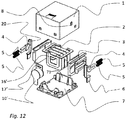
- the overvoltage protection arrangement according to the Fig. 2 and 3 and 11 and 12 are initially based on a carrier plate 7.
- This carrier plate 7 consists of a plastic injection-molded material. Slit-shaped openings 72, which are used to lead through connections 6 and 61, are made in the carrier plate 7.
- the corresponding lead-through connections 6 and 61 can be used for direct contacting and soldering on a circuit board (not shown).
- the overvoltage protection arrangement according to the Fig. 2 ; 3 and 11 ; 12 also comprises a formation of several disk-shaped varistors 2; 21; 22. These varistors form a parallel package arrangement.
- This parallel package arrangement is on two opposite sides of one insulating partition 3, which can be placed on the carrier plate 7; 31 limited.
- Each partition 3; 31 has at least one opening for a varistor connection 62, which is connected to a thermal separation device.
- thermal disconnection devices have a spring-loaded disconnection lever 80.
- the respective separating lever 80 is connected at its first end to the respective varistor connection 62 by solder 18 in the L / N path or N / L path 20.
- the respective separating lever 80 merges into one of the electrical connections 6 (L / N path), which penetrates the carrier plate 7.
- the thermal separation device also comprises an insulating slide 4, the free end of which acts on the separation lever 80, the slide 4 being guided in recesses 81 of the respective partition 3.
- a change in position of the slide 4 can be seen by means of a viewing opening in the form of a window 8 in the outer housing 1.
- the slide 4 furthermore comprises two pins for the guiding reception of one helical spring 5 in each case.
- the arrangement On its partition-free side, the arrangement has a gas discharge tube 10, which is electrically connected to the varistor package arrangement according to FIG Fig. 1 or. Fig. 10 is interconnected according to the second embodiment.
- the gas discharge tube 10 has a separate thermal and spring-force-supported disconnection device.
- the separating device for the gas discharge tube 10 has two torsion springs 9.
- the slide 4 engages in the immediate vicinity of the solder connection point between the separating lever 80 and the varistor connection 62.
- the Fig. 2 and 3 also show cutouts 13 in the outer housing 1. The cutouts serve to accommodate latching hooks 14 to form a snap-in connection.
- the reference number 10 symbolizes the low-temperature solder connection of the disconnection device for the gas discharge arrester and reference number 18 symbolizes the corresponding low-temperature solder connection for the disconnection device of the varistors.
- the torsion springs 9 according to Fig. 3 are preloaded and guided by the stub axles 11 and 12.
- Reference number 16 denotes the separation point electrode on the varistor side and reference number 17 denotes the separation point electrode on the gas discharge conductor side.
- the representation according to Fig. 11 and 12 comprises a comparable embodiment as based on Fig. 2 and 3 explained, with the difference that the gas discharge tube 10 according to Fig. 11 and 12 does not have a separate thermal disconnection device with a corresponding contact bracket and torsion spring 9.
- Fig. 4 and 6th is the thermal disconnection device for the varistors in the closed state and in the Fig. 5 and 7th shown in the open, ie separated state.
- FIG. 8 shows the state of the non-separated thermal cut-off device for the gas discharge arrester 10 and the Fig. 9 the state 15 'separated in this regard.
- the Fig. 10 shows the circuit diagram of the internal wiring according to the second embodiment, which is not part of the invention, wherein in this embodiment the gas discharge tube in the PE direction does not have a separate disconnection device. Rather, normal soldering 210 takes place here at the corresponding contact point.
- the structure of the remaining assemblies, in particular the thermal separation devices for the varistors 2 corresponds to that according to the first embodiment.
- connection part 17 'of the gas diverter 10' The soldered connection of the gas diverter 10 'according to the second embodiment to the electrode 16' of the corresponding varistor 2 is supported by a slot-shaped recess in the connection part 17 'of the gas diverter 10'.
- the inner wall of the outer housing 1 can also have a coating that reflects heat radiation and otherwise be designed to be thermally and electrically insulating.
Landscapes
- Engineering & Computer Science (AREA)
- Microelectronics & Electronic Packaging (AREA)
- Physics & Mathematics (AREA)
- Electromagnetism (AREA)
- Chemical & Material Sciences (AREA)
- Combustion & Propulsion (AREA)
- Thermistors And Varistors (AREA)
- Fuses (AREA)
- Emergency Protection Circuit Devices (AREA)
Description
- Die Erfindung betrifft eine Überspannungsschutzanordnung mit mehreren, auf einer ersten Seite einer n-eckigen Trägerplatte angeordneten, scheibenförmigen Varistoren, mindestens einem Gasableiter sowie mindestens einer Thermosicherung oder thermischen Abtrenneinrichtung, welche mit mindestens einem der Varistoren in engem thermischen Kontakt steht, wobei die vorgenannten Bauteile von einem Außengehäuse umgeben und weiterhin auf der zweiten Seite der Trägerplatte Mittel zum elektrischen Anschluss zum Verlöten auf einer Leiterplatte vorgesehen sind, gemäß Oberbegriff des Anspruchs 1.
- Aus der
CN000204668940U - Zwischen mindestens zwei der räumlich in Reihe angeordneten scheibenförmigen Varistoren ist eine Thermosicherung befindlich, welche in einem engen thermischen Kontakt zum jeweiligen Varistor steht.
- Die räumliche Reihenschaltung umfasst darüber hinaus einen Gasentladungsableiter.
- Bedingt durch die Anordnung der Thermosicherung innerhalb der Sandwich-Konstruktion der Varistoren kann nur der jeweils benachbarte Varistor hinsichtlich seines thermischen Verhaltens überwacht werden. Eine Überprüfung des Zustands des eingesetzten Gasableiters ist nicht möglich. Weiterhin führt die SandwichAnordnung der Varistoren zu Problemen beim Erreichen oder Sicherstellen notwendiger elektrischer Trennungsabstände.
- Ganz grundsätzlich kann die Wärmeenergie der thermisch zu überwachenden Varistoren gemäß dem geschilderten Stand der Technik nur unzureichend und nicht schnell genug zu den thermischen Sicherungen transportiert werden.
- Aus der
DE 10 2013 005 327 A1 ist eine Überspannungsschutzanordnung mit mehreren scheibenförmigen Varistoren vorbekannt. - Diese scheibenförmigen Varistoren sind innerhalb eines, einen Hohlraum einschließenden Gehäuses angeordnet und elektrisch kontaktiert.
- Dieses vorbekannte Gehäuse ist als Vieleckkörper, insbesondere mehrseitiges Prisma, Würfel, Quader oder Tetraeder ausgebildet und weist eine Öffnung zum Einbringen der scheibenförmigen Varistoren auf, welche jeweils mit einem Abschnitt oder einem Teil der Gehäuseinnenseitenwandung mechanisch in Verbindung stehen und dort in Anlage kommen. Über das Gehäuse kann eine elektrische Kontaktierung zur gewünschten Parallelschaltung der eingesetzten Varistoren vorgenommen werden. Darüber hinaus schaffen großflächige Verbindungen und das diesbezügliche Inkontaktkommen der Varistoren mit der Gehäuseseitenwand einen guten thermischen Übergang zum Zweck des Ableitens von Verlustwärme.
- Zum Stand der Technik sei noch auf die
DE 37 34 214 C2 verwiesen. Dieses Dokument zeigt eine Anordnung mit einem Varistor, wobei zur Abschaltung des Varistors von einer Spannungsquelle bei dessen Überhitzung die auf beiden Stirnseiten des Varistors vorgesehenen Kontaktflächen mit Zu- und Ableitungen der Spannungsquelle verbunden sind und wobei in einer dieser Leitungen in Varistornähe eine Lotstelle vorgesehen ist. Der Varistor selbst befindet sich in einem napfförmigen Gehäuse, wobei die erste seiner Kontaktflächen an der Innenseite der Gehäusebodenfläche anliegt und das Gehäuse einen Anschluss bildet bzw. aufweist. Die zweite Seite der Kontaktfläche des Varistors ist mit einer Isoliermasse abgedeckt, wobei eine elektrisch und thermisch leitende Verbindung durch die Isoliermasse hindurch zur Lotstelle besteht. Die Lotstelle und die einen Anschluss bildende Verbindung befinden sich an der dem Varistor abgewandten Oberfläche der Isoliermasse. Eine federnde Kontaktzunge der derart gebildeten thermischen Abtrennvorrichtung ist als Spiralfeder ausgebildet, wobei das äußere Ende dieser Spirale über die Lotstelle mit dem zugehörigen Anschluss und das innere Ende dieser Spirale mit dem zugehörigen Gegenanschluss verbunden ist. - Das Dokument
CN 104 008 936 A beschreibt eine Überspannungsschutzanordnung mit mehreren Varistoren, mit einem Gasableiter und mit thermischen Abtrenneinrichtungen, die einen isolierenden Schieber aufweisen. - Im Rahmen einer zunehmenden Integration von Baugruppen und Bauteilen auf Leiterplattenebene entstehen Probleme bei der Anordnung und Einbindung von Überspannungsschutzgeräten in derartige elektronische Einrichtungen. Die Überspannungsschutzgeräte müssen insofern von ihrem Bauraum möglichst klein ausgeführt werden und sollen zur unmittelbaren Leiterplattenmontage geeignet sein. Weiterhin besteht die Notwendigkeit, trotz geringer Abmessungen und einer recht hohen Packungsdichte die notwendigen elektrischen Trennungsabstände einzuhalten. Letztendlich sind bisher bekannte thermische Abtrennvorrichtungen für den Schutz von Überspannungselementen bei deren Überlastung ausreichend sensibel zu gestalten, wobei jedoch eine Beeinflussung durch umgebende Wärmequellen anderer elektronischer Baugruppen oder elektronischer Bauelemente möglichst ausgeschlossen werden soll.
- Aus dem Vorgenannten ist es daher Aufgabe der Erfindung, eine weiterentwickelte Überspannungsschutzanordnung mit mehreren, auf einer ersten Seite einer n-eckigen Trägerplatte angeordneten, scheibenförmigen Varistoren sowie mindestens einem Gasableiter sowie thermischen Abtrenneinrichtungen anzugeben, welche in einfacher Weise mit wenigen Bauteilen, reduziertem Bauraum und kostengünstig herstellbar ist. Die zu schaffende Anordnung soll als kompakte Baugruppe so ausgeführt werden, dass sie zur unmittelbaren Montage auf einer Leiterplatte einsetzbar ist. Weiterhin soll die Möglichkeit bestehen, mit einfachen Mitteln erkennen zu lassen, ob die Anordnung funktionsfähig oder ob bereits eine Schädigung durch thermische Überlastung aufgetreten ist.
- Die Lösung der Aufgabe der Erfindung erfolgt gemäß der Merkmalskombination nach Anspruch 1, wobei die Unteransprüche mindestens zweckmäßige Ausgestaltungen und Weiterbildungen umfassen.
- Die erfindungsgemäße Lösung geht von einer an sich bekannten Überspannungsschutzanordnung aus, welche mehrere, auf einer ersten Seite einer n-eckigen Trägerplatte angeordneten, scheibenförmigen Varistoren aufweist. Die Überspannungsschutzanordnung besitzt darüber hinaus noch mindestens einen Gasableiter sowie thermischen Abtrenneinrichtungen. Die thermischen Abtrenneinrichtungen stehen in bekannter Weise mit den Varistoren in engem thermischen Kontakt.
- Die vorgenannten Bauteile sind von einem Außengehäuse, das als Kappe ausgebildet sein kann, umgeben. Auf der zweiten Seite der Trägerplatte sind Mittel zum elektrischen Anschluss, z.B. ausgebildet als Kontaktstifte, vorhanden, die dem unmittelbaren Verlöten auf einer Leiterplatte dienen.
- Erfindungsgemäß bilden die Varistoren eine dicht gepackte, parallele Anordnung, nachstehend als Paketanordnung bezeichnet. Diese Paketanordnung ist auf zwei gegenüberliegenden Seiten von je einer, auf der Trägerplatte aufsetzbaren oder mit dieser verbundenen, isolierenden Trennwand begrenzt.
- Die Innenseite der Trennwand steht also mit der Paketanordnung in Verbindung. Jede Trennwand weist mindestens einen Durchbruch für einen Varistoranschluss auf, welcher mit je einer thermischen Abtrenneinrichtung in Verbindung steht, die wiederum einen federbelasteten Abtrennhebel umfasst. Es nimmt also die Außenseite der Trennwand die eigentliche thermische Abtrenneinrichtung auf. Der jeweilige Abtrennhebel ist an seinem ersten Ende mit dem jeweiligen Varistoranschluss durch ein Lot verbunden. Mit seinem zweiten Ende geht der Abtrennhebel in einen der elektrischen Anschlüsse über, welcher diesbezüglich die Trägerplatte durchdringt.
- Die thermischen Abtrenneinrichtungen besitzen darüber hinaus je einen isolierenden Schieber, dessen freies Ende auf den Abtrennhebel einwirkt, wobei der Schieber in Ausformungen der jeweiligen Seitenwand geführt ist. Diese Führung ist als Längsführung ausgebildet, so dass eine Verschiebebewegung des Schiebers in Richtung Abtrennhebel erfolgen kann.
- Die Lageveränderung des Schiebers, der z.B. als ein farblich gestaltetes Kunststoffbauteil ausgeführt sein kann, ist mittels einer Sichtöffnung im Außengehäuse erkennbar, so dass auf den Zustand der im Außengehäuse befindlichen Überspannungsschutzanordnung geschlossen werden kann.
- Bei einer bevorzugten Ausführungsform der Erfindung besteht die Paketanordnung aus drei, mit ihren Längsseiten aneinander anliegenden Varistoren.
- Erfindungsgemäß weist der Schieber zwei Zapfen zur führenden Aufnahme von jeweils einem Federelement auf, wobei die Zapfen parallel verlaufen. Die Zapfen nehmen jeweils eine Schraubenfeder auf, so dass die notwendige Vorspannung des Schiebers in Richtung Abtrennhebel gegeben ist.
- An einer trennwandfreien Seite der Anordnung befindet sich ein Gasableiter, welcher elektrisch mit der Varistor-Paketanordnung verschalten ist.
- Erfindungsgemäß verfügt der Gasableiter über eine separate thermische und federkraftunterstützte Abtrenneinrichtung.
- Der Außengehäuse ist in bevorzugter Weise mit Hilfe einer Snap-in-Rastanordnung mit der Trägerplatte verbindbar.
- Die Abtrenneinrichtung für den Gasableiter weist auf einen Abtrennmechanismus einwirkende Torsionsfedern auf. Der Schieber greift mit seinem freien Ende in unmittelbarer Nähe der Lotverbindungsstelle zwischen Abtrennhebel und Varistoranschluss an.
- Ein besonderer Aspekt der Erfindung besteht darin, dass die vorstehend erläuterte thermische Abtrenneinrichtung doppelt und symmetrisch ausgebildet ist, das heißt, dass quasi auf beiden Außenseiten der erläuterten Trennwände entsprechende Abtrenneinrichtungen je für den L/N- und N/L-Zweig realisiert werden.
- In weiterer Ausgestaltung der Erfindung erstrecken sich von der ersten Seite der Trägerplatte in Abschnitte des umschlossenen Raumes hinein Stegflächen zum Gewährleisten ausreichender elektrischer Trennungsabstände.
- Das Außengehäuse kann die Form eines n-eckigen Würfels oder Quaders aufweisen.
- In einer Ausgestaltung besitzt die Innwandung des Außengehäuses eine Wärmestrahlung-reflektierende Beschichtung oder weist Wärmestrahlung-reflektierende Eigenschaften auf. Damit ist sichergestellt, dass die thermische Abtrenneinrichtung primär auf im Gehäuse befindliche Wärmequellen und nicht auf externe Wärmequellen reagiert bzw. anspricht.
- Die erläuterte Überspannungsschutzanordnung findet insbesondere Verwendung als kompakte, gekapselte Leiterplatten-montierbare Baueinheit, wobei die Größe der Kapselung im Wesentlichen von den Abmessungen der eingesetzten Varistoren, die das Paket bilden, bestimmt und vorgegeben ist.
- Die Erfindung soll nachstehend anhand von Ausführungsbeispielen sowie unter Zuhilfenahme von Figuren näher erläutert werden.
- Hierbei zeigen:
- Fig. 1
- ein Prinzipschaltbild der Überspannungsschutzanordnung mit drei Varistoren und einem Gasableiter und den jeweiligen Pfaden;
- Fig. 2
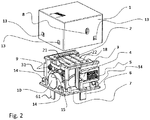
- eine perspektivische Darstellung der ersten Ausführungsform der Erfindung mit abgenommenem Außengehäuse;
- Fig. 3
- eine perspektivische Explosionsdarstellung einer ersten Ausführungsform der Erfindung mit paralleler Paketanordnung von Varistoren sowie einem Gasableiter, welcher wie die Varistoren über eine separate thermische Abtrenneinrichtung verfügt;
- Fig,. 4
- eine perspektivische Darstellung der ersten Ausführungsform mit Niedrigtemperatur-Lotverbindung der Abtrennvorrichtung im L/N-Pfad im geschlossenen Zustand;
- Fig. 5
- eine Darstellung gemäß derjenigen nach
Fig. 4 , jedoch im abgetrennten Zustand 19 des L/N-Pfades; - Fig. 6
- eine perspektivische Darstellung der ersten Ausführungsform der Erfindung mit Niedrigtemperatur-Trennstrecke im N/L-Pfad im nicht abgetrennten Zustand 18';
- Fig. 7
- eine Darstellung ähnlich derjenigen nach
Fig. 6 , jedoch im abgetrennten Zustand 19' des Pfades N/L; - Fig. 8
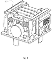
- eine perspektivische Darstellung der ersten Ausführungsform der Erfindung mit thermischer Abtrennvorrichtung für den Gasableiter im geschlossenen Zustand;
- Fig. 9
- eine Darstellung ähnlich derjenigen nach
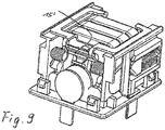
Fig. 8 , jedoch im abgetrennten Zustand 15' (Pfeildarstellung); - Fig. 10
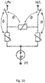
- ein Prinzipschaltbild einer Ausführungsform der Überspannungsschutzanordnung mit thermischer Abtrenneinrichtung nur für die Varistoren, d.h. ohne thermische Abtrennung des Gasableiters und die Beschaltung in den Pfaden L/N, N/L und PE;
- Fig. 11
- eine perspektivische Darstellung der zweiten Ausführungsform, die einen Gasableiter ohne separate thermische Abtrennvorrichtung zeigt und die kein Teil der Erfindung ist.
- Fig. 12
- eine perspektivische Explosionsdarstellung der Ausführungsform mit einem Gasableiter ohne separate thermische Abtrenneinrichtung;
- Fig. 13
- eine Darstellung gemäß zweiter Ausführungsform mit geschlossener thermischer Abtrennvorrichtung 230 im L/N-Pfad;
- Fig. 14
- eine Darstellung ähnlich derjenigen nach
Fig. 13 , jedoch im abgetrennten Zustand 240 (Pfeildarstellung) des L/N-Pfades; - Fig. 15
- eine perspektivische Darstellung der Abtrennvorrichtung gemäß der zweiten Ausführungsform mit geschlossener Abtrennvorrichtung 230' im N/L-Pfad und
- Fig. 16
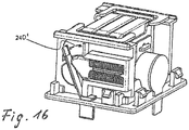
- eine Darstellung ähnlich derjenigen nach
Fig. 15 , jedoch im abgetrennten Zustand 240' des N/L-Pfades. - Die
Fig. 1 zeigt ein Prinzipschaltbild der ersten Ausführungsform der Erfindung mit drei Varistoren und einem Gasableiter, wobei im L/N-Pfad sowie im N/L-Pfad jeweils eine thermische Abtrennvorrichtung für die Varistoren und in Richtung PE eine thermische Abtrennvorrichtung für den Gasableiter vorhanden ist. Die ab trennseitig energetische Einwirkung der Varistoren auf die entsprechenden Abtrennvorrichtungen im Zweig L/N bzw. N/L ist mit den symbolischen gestrichelten Pfeildarstellungen gezeigt und in analoger Weise bezogen auf den Gasableiter in Richtung PE symbolisiert. - Die Überspannungsschutzanordnung nach den
Fig. 2 und3 sowie 11 uns 12 geht zunächst von einer Trägerplatte 7 aus. - Diese Trägerplatte 7 besteht aus einem Kunststoff-Spritzgussmaterial. In der Trägerplatte 7 sind schlitzförmige Öffnungen 72 eingebracht, die der Durchführung von Anschlüssen 6 und 61 dienen.
- Die entsprechenden durchgeführten Anschlüsse 6 und 61 können zur unmittelbaren Kontaktierung und dem Verlöten auf einer Leiterplatte (nicht gezeigt) genutzt werden.
- Die Überspannungsschutzanordnung nach den
Fig. 2 ;3 und11 ;12 umfasst darüber hinaus eine Ausbildung mehrerer scheibenförmiger Varistoren 2; 21; 22. Diese Varistoren bilden eine parallele Paketanordnung. - Diese parallele Paketanordnung ist auf zwei gegenüberliegenden Seiten von je einer, auf der Trägerplatte 7 aufsetzbaren isolierenden Trennwand 3; 31 begrenzt.
- Jede Trennwand 3; 31 besitzt mindestens einen Durchbruch für einen Varistoranschluss 62, welcher mit je einer thermischen Abtrenneinrichtung in Verbindung steht.
- Diese thermischen Abtrenneinrichtungen verfügen über einen federbelasteten Abtrennhebel 80.
- Der jeweilige Abtrennhebel 80 ist an seinem ersten Ende mit dem jeweiligen Varistoranschluss 62 durch Lot 18 im L/N-Pfad bzw. N/L-Pfad 20 verbunden.
- An seinem zweiten Ende geht der jeweilige Abtrennhebel 80 in einen der elektrischen Anschlüsse 6 (L/N-Pfad) über, welcher die Trägerplatte 7 durchdringt.
- Die thermische Abtrenneinrichtung umfasst darüber hinaus einen isolierenden Schieber 4, dessen freies Ende auf den Abtrennhebel 80 einwirkt, wobei der Schieber 4 in Ausformungen 81 der jeweiligen Trennwand 3 geführt ist.
- Eine Lageveränderung des Schiebers 4 ist mittels einer Sichtöffnung in Form eines Fensters 8 im Außengehäuse 1 erkennbar.
- Der Schieber 4 umfasst weiterhin zwei Zapfen zur führenden Aufnahme von jeweils einer Schraubenfeder 5.
- An ihrer trennwandfreien Seite weist die Anordnung einen Gasableiter 10 auf, welcher elektrisch mit der Varistor-Paketanordnung gemäß
Fig. 1 bzw.Fig. 10 nach der zweiten Ausführungsform verschalten ist. - Der Gasableiter 10 verfügt über eine separate thermische und federkraftunterstützte Abtrenneinrichtung.
- Diesbezüglich weist die Abtrenneinrichtung für den Gasableiter 10 zwei Torsionsfedern 9 auf.
- Wie aus den
Fig. 2 und3 ersichtlich, greift der Schieber 4 in unmittelbarer Nähe der Lotverbindungsstelle zwischen Abtrennhebel 80 und Varistoranschluss 62 an. DieFig. 2 und3 zeigen noch Aussparungen 13 im Außengehäuse 1. Die Aussparungen dienen der Aufnahme von Rasthaken 14 zur Bildung einer Snap-in-Verbindung. Mit dem Bezugszeichen 10 ist die Niedrigtemperatur-Lotverbindung der Abtrennvorrichtung für den Gasentladungsableiter und mit dem Bezugszeichen 18 die entsprechende Niedrigtemperatur-Lotverbindung für die Abtrennvorrichtung der Varistoren symbolisiert. Die Torsionsfedern 9 gemäßFig. 3 werden von den Achsstummeln 11 und 12 vorgespannt und geführt. Mit dem Bezugszeichen 16 wird die Trennstellenelektrode varistorseitig und mit dem Bezugszeichen 17 die Trennstellenelektrode gasentladungsableiterseitig bezeichnet. - Die Darstellung gemäß
Fig. 11 und12 umfasst eine vergleichbare Ausführungsform wie anhand derFig. 2 und3 erläutert, mit dem Unterschied, dass der Gasableiter 10 gemäßFig. 11 und12 über keine separate thermische Abtrenneinrichtung mit entsprechendem Kontaktbügel und Torsionsfeder 9 verfügt. - In den
Fig. 4 und6 ist die thermische Abtrenneinrichtung für die Varistoren im geschlossenen Zustand und in denFig. 5 und7 im geöffneten, d.h. abgetrennten Zustand dargestellt. - Die
Fig. 8 zeigt den Zustand der nicht abgetrennten thermischen Abtrennvorrichtung für den Gasentladungsableiter 10 und dieFig. 9 den diesbezüglich abgetrennten Zustand 15'. - Die
Fig. 10 zeigt das Schaltbild der inneren Verdrahtung gemäß der zweiten Ausführungsform, die kein Teil der Erfindung ist, wobei bei dieser Ausführungsform der in PE-Richtung liegende Gasableiter keine separate Abtrennvorrichtung besitzt. Vielmehr findet hier ein normales Verlöten 210 an der entsprechenden Kontaktstelle statt. Der Aufbau der übrigen Baugruppen, insbesondere der thermischen Abtrennvorrichtungen für die Varistoren 2 entspricht derjenigen gemäß der ersten Ausführungsform. - Der nicht abgetrennte Zustand 230 und 230' ist in den
Fig. 13 und15 und der abgetrennte Zustand 240 und 240' in denFig. 14 und16 dargestellt. - Die Lotverbindung des Gasableiters 10' gemäß zweiter Ausführungsform mit der Elektrode 16' des entsprechenden Varistors 2 wird unterstützt durch eine schlitzförmige Ausnehmung im Anschlussteil 17' des Gasableiters 10'.
- Die Innenwandung des Außengehäuses 1 kann noch eine Wärmestrahlungsreflektierende Beschichtung aufweisen und ansonsten thermisch und elektrisch isolierend ausgebildet sein.
Claims (7)
- Überspannungsschutzanordnung mit mehreren, auf einer ersten Seite einer n-eckigen Trägerplatte (7) angeordneten, scheibenförmigen Varistoren (2; 21; 22), mindestens einem Gasableiter (10) sowie thermischen Abtrenneinrichtungen, welche mit den Varistoren in engem thermischen Kontakt stehen, wobei die vorgenannten Bauteile von einem Außengehäuse (1) umgeben und weiterhin auf der zweiten Seite der Trägerplatte (7) Mittel zum elektrischen Anschluss zum Verlöten auf einer Leiterplatte vorgesehen sind, wobei die Varistoren (2; 21; 22) eine parallele Paketanordnung bilden, welche auf zwei gegenüberliegenden Seiten von je einer, auf der Trägerplatte (7) aufsetzbaren, isolierenden Trennwand (3; 31) begrenzt ist,
jede Trennwand (3: 31) mindestens einen Durchbruch für einen Varistoranschluss (62) aufweist, welcher mit je einer thermischen Abtrenneinrichtung in Verbindung steht, die wiederum einen federbelasteten Abtrennhebel (80) umfasst, wobei der jeweilige Abtrennhebel (80) an seinem ersten Ende mit dem jeweiligen Varistoranschluss (62) durch ein Lot verbunden ist und mit seinem zweiten Ende in einen der elektrischen Anschlüsse (6) übergeht und diesbezüglich die Trägerplatte (7) durchdringt, weiterhin
die thermischen Abtrenneinrichtungen je einen isolierenden Schieber (4) besitzen, dessen freies Ende auf den jeweiligen Abtrennhebel (80) einwirkt,
dadurch gekennzeichnet, dass
die Schieber (4) in Ausformungen (81) der jeweiligen Trennwand (3; 31) geführt sind und eine Lageveränderung des Schiebers (4) mittels einer Sichtöffnung (8) im Außengehäuse (1) erkennbar ist, die Schieber (4) zwei Zapfen zur führenden Aufnahme von jeweils einem Federelement (5) besitzen, wobei die Zapfen parallel verlaufen und an einer trennwandfreien Seite der Gasableiter (10) befindlich ist, welcher elektrisch mit der Varistor-Paketanordnung verschalten ist und welcher über eine separate thermische und federkraftunterstützte Abtrenneinrichtung mit auf Achsstummeln (11; 12) vorgespannten und geführten Torsionsfedern (9) verfügt. - Überspannungsschutzanordnung nach Anspruch 1,
dadurch gekennzeichnet, dass
die Paketanordnung aus drei, mit ihren Längsseiten aneinander liegenden Varistoren (2; 21;22) gebildet ist. - Überspannungsschutzanordnung nach einem der vorangegangenen Ansprüche,
dadurch gekennzeichnet, dass
das Außengehäuse (1) mittels Snap-in-Rastanordnung (13; 14) mit der Trägerplatte (7) verbindbar ist. - Überspannungsschutzanordnung nach einem der vorangegangenen Ansprüche,
dadurch gekennzeichnet, dass
der Schieber (4) in unmittelbarer Nähe der Lotverbindungsstelle zwischen Abtrennhebel (80) und Varistoranschluss (62) angreift. - Überspannungsschutzanordnung nach einem der vorangegangenen Ansprüche,
dadurch gekennzeichnet, dass
sich von der ersten Seite der Trägerplatte (7) in Abschnitte des umschlossenen Raumes hinein Stegflächen (71) zum Gewährleisten ausreichender elektrischer Trennungsabstände erstrecken. - Überspannungsschutzanordnung nach einem der vorangegangenen Ansprüche,
dadurch gekennzeichnet, dass
die Innenwandung des Außengehäuses (1) eine Wärmestrahlung-reflektierende Beschichtung oder Wärmestrahlung-reflektierende Eigenschaften besitzt. - Überspannungsschutzanordnung nach einem der vorangegangenen Ansprüche, gekennzeichnet durch deren Einsatz als kompakte, gekapselte Leiterplatten-montierbare Einheit, wobei die Größe der Kapselung im Wesentlichen von den Abmessungen der eingesetzten Varistoren bestimmt und vorgegeben ist.
Priority Applications (1)
| Application Number | Priority Date | Filing Date | Title |
|---|---|---|---|
| SI201730489T SI3469605T1 (sl) | 2016-06-10 | 2017-05-22 | Razmestitev prenapetostne zaščite z več ploščatimi varistorji, razmeščenimi na prvi stranici N-oglate nosilne plošče |
Applications Claiming Priority (3)
| Application Number | Priority Date | Filing Date | Title |
|---|---|---|---|
| DE102016007131 | 2016-06-10 | ||
| DE102016015593.0A DE102016015593B4 (de) | 2016-06-10 | 2016-12-29 | Überspannungsschutzanordnung mit mehreren, auf einer ersten Seite einer n-eckigen Trägerplatte angeordeten, scheibenförmigen Varistoren |
| PCT/EP2017/062247 WO2017211578A1 (de) | 2016-06-10 | 2017-05-22 | Überspannungsschutzanordnung mit mehreren, auf einer ersten seite einer n-eckigen trägerplatte angeordneten, scheibenförmigen varistoren |
Publications (2)
| Publication Number | Publication Date |
|---|---|
| EP3469605A1 EP3469605A1 (de) | 2019-04-17 |
| EP3469605B1 true EP3469605B1 (de) | 2020-10-14 |
Family
ID=60419653
Family Applications (1)
| Application Number | Title | Priority Date | Filing Date |
|---|---|---|---|
| EP17726589.9A Not-in-force EP3469605B1 (de) | 2016-06-10 | 2017-05-22 | Überspannungsschutzanordnung mit mehreren, auf einer ersten seite einer n-eckigen trägerplatte angeordneten, scheibenförmigen varistoren |
Country Status (6)
| Country | Link |
|---|---|
| US (1) | US10629399B2 (de) |
| EP (1) | EP3469605B1 (de) |
| CN (1) | CN109313969B (de) |
| DE (1) | DE102016015593B4 (de) |
| SI (1) | SI3469605T1 (de) |
| WO (1) | WO2017211578A1 (de) |
Families Citing this family (10)
| Publication number | Priority date | Publication date | Assignee | Title |
|---|---|---|---|---|
| FR3057403B1 (fr) * | 2016-10-10 | 2019-10-18 | Citel | Composant integrant une varistance thermoprotegee et un eclateur en serie |
| CN110350501B (zh) * | 2018-04-04 | 2022-04-05 | 爱普科斯电子元器件(珠海保税区)有限公司 | 三相电涌保护装置 |
| DE102018125520A1 (de) * | 2018-10-15 | 2020-04-16 | Dehn Se + Co Kg | Überspannungsschutzgerät mit mehreren Überspannungsableitern und diesen jeweils zugeordneter, insbesondere thermischer, Abtrennvorrichtung |
| FR3094148B1 (fr) * | 2019-03-20 | 2021-04-16 | Citel | Dispositif de protection contre les surtensions |
| CN211209291U (zh) * | 2019-12-26 | 2020-08-07 | 厦门赛尔特电子有限公司 | 一种模组化浪涌保护器 |
| CN112822894B (zh) * | 2021-02-08 | 2025-05-13 | 吴蕴岭 | 电涌保护模块及电涌保护器 |
| CN216145603U (zh) * | 2021-08-31 | 2022-03-29 | 厦门赛尔特电子有限公司 | 一种热保护型的瞬态电压抑制器 |
| CN216719925U (zh) * | 2021-12-14 | 2022-06-10 | 厦门赛尔特电子有限公司 | 一种热保护瞬态电压抑制器 |
| US12506334B2 (en) | 2022-01-24 | 2025-12-23 | Raycap IP Development Ltd | Surge protective device modules and assemblies |
| CN118197870B (zh) * | 2024-04-16 | 2025-06-20 | 加西亚电子电器股份有限公司 | 一种智能物联网断路器 |
Family Cites Families (21)
| Publication number | Priority date | Publication date | Assignee | Title |
|---|---|---|---|---|
| GB2178913A (en) * | 1985-07-23 | 1987-02-18 | Sydney Stanley Bosley | Electrical fuse |
| DE3734214A1 (de) | 1987-10-09 | 1989-04-20 | Dehn & Soehne | Anordnung zur abschaltung eines varistors |
| JP2512887B2 (ja) * | 1991-09-17 | 1996-07-03 | 三菱マテリアル株式会社 | サ―ジ吸収器 |
| US5311393A (en) * | 1992-04-08 | 1994-05-10 | Atlantic Sientific Corporation | Transient voltage surge suppressor with I2 R/I2 T overcurrent protection switch |
| US20020011915A1 (en) * | 1997-04-11 | 2002-01-31 | Masahiko Niino | Thermal Protector |
| US6249415B1 (en) * | 1999-05-10 | 2001-06-19 | Avaya Technology Corp. | Surge protector and method for preventing damage from line surges |
| DE102007042991B4 (de) * | 2007-06-11 | 2009-09-17 | Dehn + Söhne Gmbh + Co. Kg | Überspannungsschutzgerät mit im thermischen Überlastfall aktivierter mechanischer Abtrennvorrichtung |
| US7974063B2 (en) * | 2007-11-16 | 2011-07-05 | Corning Cable Systems, Llc | Hybrid surge protector for a network interface device |
| DE102008026555B4 (de) | 2008-06-03 | 2016-08-04 | DEHN + SÖHNE GmbH + Co. KG. | Überspannungsschutzgerät mit thermischer Abtrennvorrichtung |
| DE102008047396B3 (de) * | 2008-08-22 | 2010-03-11 | Dehn + Söhne Gmbh + Co. Kg | Überspannungsschutzgerät mit thermischer Abtrennvorrichtung |
| CZ2009164A3 (cs) * | 2009-03-16 | 2010-09-29 | Cernicka@Jozef | Zarízení pro prepetovou ochranu |
| DE102009035060A1 (de) * | 2009-07-28 | 2011-02-03 | Phoenix Contact Gmbh & Co. Kg | Überspannungschutzelement |
| DE102009036125A1 (de) * | 2009-08-05 | 2011-02-10 | Phoenix Contact Gmbh & Co. Kg | Überspannungsschutzelement |
| SI23749A (sl) | 2011-05-11 | 2012-11-30 | ISKRA@ZAŠČITE@d@o@o | Redudančni prenapetostni odklopnik z rotacijskimdiskom in z dodanim elektronskim sklopom za zagotavljanje podaljšanja življenjske dobe prenapetostnega gradnika |
| WO2014063362A1 (en) * | 2012-10-26 | 2014-05-01 | Littelfuse, Inc. | Surge protection device |
| DE102013005327A1 (de) | 2012-11-29 | 2014-06-05 | Dehn + Söhne Gmbh + Co. Kg | Überspannungsschutzanordnung mit scheibenförmigem Varistor |
| DE102013006052B4 (de) * | 2013-02-08 | 2016-08-04 | DEHN + SÖHNE GmbH + Co. KG. | Überspannungsschutzgerät |
| CN104008936B (zh) | 2014-06-13 | 2016-04-06 | 四川中光防雷科技股份有限公司 | 脱离与遮弧装置及全模保护电涌保护器 |
| DE102015000329B3 (de) | 2015-01-09 | 2016-05-19 | DEHN + SÖHNE GmbH + Co. KG. | Überspannungsschutzgerät mit im thermischen Überlastfall aktivierter mechanischer Abtrennvorrichtung |
| WO2016161546A1 (en) * | 2015-04-07 | 2016-10-13 | Dongguan Littelfuse Electronics, Co., Ltd | Surge protection device |
| CN204668940U (zh) * | 2015-05-19 | 2015-09-23 | 菲尼克斯亚太电气(南京)有限公司 | 电路板用小型防浪涌保护器 |
-
2016
- 2016-12-29 DE DE102016015593.0A patent/DE102016015593B4/de not_active Expired - Fee Related
-
2017
- 2017-05-22 CN CN201780035783.9A patent/CN109313969B/zh not_active Expired - Fee Related
- 2017-05-22 WO PCT/EP2017/062247 patent/WO2017211578A1/de not_active Ceased
- 2017-05-22 US US16/306,299 patent/US10629399B2/en not_active Expired - Fee Related
- 2017-05-22 SI SI201730489T patent/SI3469605T1/sl unknown
- 2017-05-22 EP EP17726589.9A patent/EP3469605B1/de not_active Not-in-force
Non-Patent Citations (1)
| Title |
|---|
| None * |
Also Published As
| Publication number | Publication date |
|---|---|
| US20190295792A1 (en) | 2019-09-26 |
| DE102016015593A1 (de) | 2017-12-14 |
| SI3469605T1 (sl) | 2020-12-31 |
| CN109313969B (zh) | 2020-09-22 |
| CN109313969A (zh) | 2019-02-05 |
| DE102016015593B4 (de) | 2021-07-08 |
| EP3469605A1 (de) | 2019-04-17 |
| US10629399B2 (en) | 2020-04-21 |
| WO2017211578A1 (de) | 2017-12-14 |
Similar Documents
| Publication | Publication Date | Title |
|---|---|---|
| DE102016015593B4 (de) | Überspannungsschutzanordnung mit mehreren, auf einer ersten Seite einer n-eckigen Trägerplatte angeordeten, scheibenförmigen Varistoren | |
| DE10001667C1 (de) | Mehrpoliger Überspannungsableiter zum Einsatz in Niederspannungs-Stromversorgungssystemen | |
| DE69117543T2 (de) | Verbinder mit auswechselbaren kontakten | |
| DE102011100437B4 (de) | Anordnung zur Ausbildung einer thermischen Trennstelle | |
| DE102006034164B4 (de) | Mehrpoliger Blitzstrom- und/oder Überspannungsableiter in Reihenklemmausführung | |
| DE102013108383A1 (de) | Steckverbindermodul | |
| WO2012110135A1 (de) | Überspannungsschutzeinrichtung, umfassend mindestens einen überspannungsableiter | |
| DE202014002496U1 (de) | Überspannungsschutzeinrichtung, umfassend mindestens einen Überspannungsableiter und eine dem Überspannungsableiter parallel geschaltete, thermisch auslösbare, federvorgespannte Kurzschliessschalteinrichtung | |
| EP2608323B1 (de) | Gehäusedurchführungsverbinder | |
| DE102010044612A1 (de) | Elektrisch leitende Kontaktanordnung | |
| DE102013019390B4 (de) | Überspannungsschutzeinrichtung, aufweisend mindestens einen Überspannungsableiter und eine, mit dem Überspannungsableiter in Reihe geschaltete, thermisch auslösbare Schalteinrichtung | |
| DE29519313U1 (de) | Überspannungsableiter | |
| EP3510676B1 (de) | Überspannungsschutzmodul für einen modularen steckverbinder | |
| WO1997041581A1 (de) | Pyrotechnisches sicherungselement für stromkreise | |
| EP3286803B1 (de) | Reihenklemme mit externem elektrischem bauelement | |
| EP2038972A1 (de) | Gerät zum schutz gegen überspannungen für elektrische anlagen | |
| DE202012000571U1 (de) | Elektrisches Sicherungselement | |
| EP0399205B1 (de) | Stellungsgeber für eine schlagwettergeschützte, elektrische Steckverbindung | |
| DE202016001937U1 (de) | Überspannungsschutzanordnung mit mehreren, auf einer ersten Seite einer n-eckigen Trägerplatte angeordneten, scheibenförmigen Varistoren | |
| DE102017113852B4 (de) | Überspannungsschutzelement | |
| DE10125941B4 (de) | Kompaktanordnung für mehrpolige stoßstromfeste Überspannungsableiter | |
| WO2011151262A1 (de) | Gehäuseanordnung für mehrpolige überspannungsschutzgeräte | |
| EP3475959B1 (de) | Überspannungsschutzanordnung mit mindestens einem, auf einer ersten seite einer n-eckigen trägerplatte angeordneten, scheibenförmigen varistor | |
| DE202014101167U1 (de) | Vorrichtung zur Ableitung von Überspannungen | |
| DE102012202240A1 (de) | Klemmkörper für eine Anschlussklemme |
Legal Events
| Date | Code | Title | Description |
|---|---|---|---|
| STAA | Information on the status of an ep patent application or granted ep patent |
Free format text: STATUS: UNKNOWN |
|
| STAA | Information on the status of an ep patent application or granted ep patent |
Free format text: STATUS: THE INTERNATIONAL PUBLICATION HAS BEEN MADE |
|
| PUAI | Public reference made under article 153(3) epc to a published international application that has entered the european phase |
Free format text: ORIGINAL CODE: 0009012 |
|
| STAA | Information on the status of an ep patent application or granted ep patent |
Free format text: STATUS: REQUEST FOR EXAMINATION WAS MADE |
|
| 17P | Request for examination filed |
Effective date: 20181126 |
|
| AK | Designated contracting states |
Kind code of ref document: A1 Designated state(s): AL AT BE BG CH CY CZ DE DK EE ES FI FR GB GR HR HU IE IS IT LI LT LU LV MC MK MT NL NO PL PT RO RS SE SI SK SM TR |
|
| AX | Request for extension of the european patent |
Extension state: BA ME |
|
| RAP1 | Party data changed (applicant data changed or rights of an application transferred) |
Owner name: DEHN SE + CO KG |
|
| DAV | Request for validation of the european patent (deleted) | ||
| DAX | Request for extension of the european patent (deleted) | ||
| GRAP | Despatch of communication of intention to grant a patent |
Free format text: ORIGINAL CODE: EPIDOSNIGR1 |
|
| STAA | Information on the status of an ep patent application or granted ep patent |
Free format text: STATUS: GRANT OF PATENT IS INTENDED |
|
| INTG | Intention to grant announced |
Effective date: 20200507 |
|
| GRAS | Grant fee paid |
Free format text: ORIGINAL CODE: EPIDOSNIGR3 |
|
| GRAA | (expected) grant |
Free format text: ORIGINAL CODE: 0009210 |
|
| STAA | Information on the status of an ep patent application or granted ep patent |
Free format text: STATUS: THE PATENT HAS BEEN GRANTED |
|
| AK | Designated contracting states |
Kind code of ref document: B1 Designated state(s): AL AT BE BG CH CY CZ DE DK EE ES FI FR GB GR HR HU IE IS IT LI LT LU LV MC MK MT NL NO PL PT RO RS SE SI SK SM TR |
|
| REG | Reference to a national code |
Ref country code: GB Ref legal event code: FG4D Free format text: NOT ENGLISH |
|
| REG | Reference to a national code |
Ref country code: AT Ref legal event code: REF Ref document number: 1324381 Country of ref document: AT Kind code of ref document: T Effective date: 20201015 Ref country code: CH Ref legal event code: EP |
|
| REG | Reference to a national code |
Ref country code: DE Ref legal event code: R096 Ref document number: 502017007755 Country of ref document: DE |
|
| REG | Reference to a national code |
Ref country code: IE Ref legal event code: FG4D Free format text: LANGUAGE OF EP DOCUMENT: GERMAN |
|
| REG | Reference to a national code |
Ref country code: NL Ref legal event code: MP Effective date: 20201014 |
|
| PG25 | Lapsed in a contracting state [announced via postgrant information from national office to epo] |
Ref country code: GR Free format text: LAPSE BECAUSE OF FAILURE TO SUBMIT A TRANSLATION OF THE DESCRIPTION OR TO PAY THE FEE WITHIN THE PRESCRIBED TIME-LIMIT Effective date: 20210115 Ref country code: FI Free format text: LAPSE BECAUSE OF FAILURE TO SUBMIT A TRANSLATION OF THE DESCRIPTION OR TO PAY THE FEE WITHIN THE PRESCRIBED TIME-LIMIT Effective date: 20201014 Ref country code: NO Free format text: LAPSE BECAUSE OF FAILURE TO SUBMIT A TRANSLATION OF THE DESCRIPTION OR TO PAY THE FEE WITHIN THE PRESCRIBED TIME-LIMIT Effective date: 20210114 Ref country code: PT Free format text: LAPSE BECAUSE OF FAILURE TO SUBMIT A TRANSLATION OF THE DESCRIPTION OR TO PAY THE FEE WITHIN THE PRESCRIBED TIME-LIMIT Effective date: 20210215 Ref country code: RS Free format text: LAPSE BECAUSE OF FAILURE TO SUBMIT A TRANSLATION OF THE DESCRIPTION OR TO PAY THE FEE WITHIN THE PRESCRIBED TIME-LIMIT Effective date: 20201014 |
|
| REG | Reference to a national code |
Ref country code: LT Ref legal event code: MG4D |
|
| PG25 | Lapsed in a contracting state [announced via postgrant information from national office to epo] |
Ref country code: SE Free format text: LAPSE BECAUSE OF FAILURE TO SUBMIT A TRANSLATION OF THE DESCRIPTION OR TO PAY THE FEE WITHIN THE PRESCRIBED TIME-LIMIT Effective date: 20201014 Ref country code: BG Free format text: LAPSE BECAUSE OF FAILURE TO SUBMIT A TRANSLATION OF THE DESCRIPTION OR TO PAY THE FEE WITHIN THE PRESCRIBED TIME-LIMIT Effective date: 20210114 Ref country code: LV Free format text: LAPSE BECAUSE OF FAILURE TO SUBMIT A TRANSLATION OF THE DESCRIPTION OR TO PAY THE FEE WITHIN THE PRESCRIBED TIME-LIMIT Effective date: 20201014 Ref country code: PL Free format text: LAPSE BECAUSE OF FAILURE TO SUBMIT A TRANSLATION OF THE DESCRIPTION OR TO PAY THE FEE WITHIN THE PRESCRIBED TIME-LIMIT Effective date: 20201014 Ref country code: IS Free format text: LAPSE BECAUSE OF FAILURE TO SUBMIT A TRANSLATION OF THE DESCRIPTION OR TO PAY THE FEE WITHIN THE PRESCRIBED TIME-LIMIT Effective date: 20210214 Ref country code: ES Free format text: LAPSE BECAUSE OF FAILURE TO SUBMIT A TRANSLATION OF THE DESCRIPTION OR TO PAY THE FEE WITHIN THE PRESCRIBED TIME-LIMIT Effective date: 20201014 |
|
| PG25 | Lapsed in a contracting state [announced via postgrant information from national office to epo] |
Ref country code: NL Free format text: LAPSE BECAUSE OF FAILURE TO SUBMIT A TRANSLATION OF THE DESCRIPTION OR TO PAY THE FEE WITHIN THE PRESCRIBED TIME-LIMIT Effective date: 20201014 Ref country code: HR Free format text: LAPSE BECAUSE OF FAILURE TO SUBMIT A TRANSLATION OF THE DESCRIPTION OR TO PAY THE FEE WITHIN THE PRESCRIBED TIME-LIMIT Effective date: 20201014 |
|
| REG | Reference to a national code |
Ref country code: DE Ref legal event code: R097 Ref document number: 502017007755 Country of ref document: DE |
|
| PG25 | Lapsed in a contracting state [announced via postgrant information from national office to epo] |
Ref country code: SM Free format text: LAPSE BECAUSE OF FAILURE TO SUBMIT A TRANSLATION OF THE DESCRIPTION OR TO PAY THE FEE WITHIN THE PRESCRIBED TIME-LIMIT Effective date: 20201014 Ref country code: SK Free format text: LAPSE BECAUSE OF FAILURE TO SUBMIT A TRANSLATION OF THE DESCRIPTION OR TO PAY THE FEE WITHIN THE PRESCRIBED TIME-LIMIT Effective date: 20201014 Ref country code: RO Free format text: LAPSE BECAUSE OF FAILURE TO SUBMIT A TRANSLATION OF THE DESCRIPTION OR TO PAY THE FEE WITHIN THE PRESCRIBED TIME-LIMIT Effective date: 20201014 Ref country code: LT Free format text: LAPSE BECAUSE OF FAILURE TO SUBMIT A TRANSLATION OF THE DESCRIPTION OR TO PAY THE FEE WITHIN THE PRESCRIBED TIME-LIMIT Effective date: 20201014 Ref country code: EE Free format text: LAPSE BECAUSE OF FAILURE TO SUBMIT A TRANSLATION OF THE DESCRIPTION OR TO PAY THE FEE WITHIN THE PRESCRIBED TIME-LIMIT Effective date: 20201014 |
|
| PGFP | Annual fee paid to national office [announced via postgrant information from national office to epo] |
Ref country code: DE Payment date: 20210525 Year of fee payment: 5 Ref country code: IT Payment date: 20210531 Year of fee payment: 5 Ref country code: CZ Payment date: 20210511 Year of fee payment: 5 Ref country code: FR Payment date: 20210521 Year of fee payment: 5 |
|
| PLBE | No opposition filed within time limit |
Free format text: ORIGINAL CODE: 0009261 |
|
| STAA | Information on the status of an ep patent application or granted ep patent |
Free format text: STATUS: NO OPPOSITION FILED WITHIN TIME LIMIT |
|
| PG25 | Lapsed in a contracting state [announced via postgrant information from national office to epo] |
Ref country code: DK Free format text: LAPSE BECAUSE OF FAILURE TO SUBMIT A TRANSLATION OF THE DESCRIPTION OR TO PAY THE FEE WITHIN THE PRESCRIBED TIME-LIMIT Effective date: 20201014 |
|
| PGFP | Annual fee paid to national office [announced via postgrant information from national office to epo] |
Ref country code: SI Payment date: 20210512 Year of fee payment: 5 |
|
| 26N | No opposition filed |
Effective date: 20210715 |
|
| PG25 | Lapsed in a contracting state [announced via postgrant information from national office to epo] |
Ref country code: AL Free format text: LAPSE BECAUSE OF FAILURE TO SUBMIT A TRANSLATION OF THE DESCRIPTION OR TO PAY THE FEE WITHIN THE PRESCRIBED TIME-LIMIT Effective date: 20201014 |
|
| REG | Reference to a national code |
Ref country code: CH Ref legal event code: PL |
|
| GBPC | Gb: european patent ceased through non-payment of renewal fee |
Effective date: 20210522 |
|
| PG25 | Lapsed in a contracting state [announced via postgrant information from national office to epo] |
Ref country code: LU Free format text: LAPSE BECAUSE OF NON-PAYMENT OF DUE FEES Effective date: 20210522 Ref country code: LI Free format text: LAPSE BECAUSE OF NON-PAYMENT OF DUE FEES Effective date: 20210531 Ref country code: MC Free format text: LAPSE BECAUSE OF FAILURE TO SUBMIT A TRANSLATION OF THE DESCRIPTION OR TO PAY THE FEE WITHIN THE PRESCRIBED TIME-LIMIT Effective date: 20201014 Ref country code: CH Free format text: LAPSE BECAUSE OF NON-PAYMENT OF DUE FEES Effective date: 20210531 |
|
| REG | Reference to a national code |
Ref country code: BE Ref legal event code: MM Effective date: 20210531 |
|
| PG25 | Lapsed in a contracting state [announced via postgrant information from national office to epo] |
Ref country code: IE Free format text: LAPSE BECAUSE OF NON-PAYMENT OF DUE FEES Effective date: 20210522 Ref country code: GB Free format text: LAPSE BECAUSE OF NON-PAYMENT OF DUE FEES Effective date: 20210522 |
|
| PG25 | Lapsed in a contracting state [announced via postgrant information from national office to epo] |
Ref country code: BE Free format text: LAPSE BECAUSE OF NON-PAYMENT OF DUE FEES Effective date: 20210531 |
|
| REG | Reference to a national code |
Ref country code: DE Ref legal event code: R119 Ref document number: 502017007755 Country of ref document: DE |
|
| PG25 | Lapsed in a contracting state [announced via postgrant information from national office to epo] |
Ref country code: CZ Free format text: LAPSE BECAUSE OF NON-PAYMENT OF DUE FEES Effective date: 20220522 |
|
| PG25 | Lapsed in a contracting state [announced via postgrant information from national office to epo] |
Ref country code: SI Free format text: LAPSE BECAUSE OF NON-PAYMENT OF DUE FEES Effective date: 20220523 |
|
| PG25 | Lapsed in a contracting state [announced via postgrant information from national office to epo] |
Ref country code: FR Free format text: LAPSE BECAUSE OF NON-PAYMENT OF DUE FEES Effective date: 20220531 |
|
| PG25 | Lapsed in a contracting state [announced via postgrant information from national office to epo] |
Ref country code: DE Free format text: LAPSE BECAUSE OF NON-PAYMENT OF DUE FEES Effective date: 20221201 |
|
| PG25 | Lapsed in a contracting state [announced via postgrant information from national office to epo] |
Ref country code: CY Free format text: LAPSE BECAUSE OF FAILURE TO SUBMIT A TRANSLATION OF THE DESCRIPTION OR TO PAY THE FEE WITHIN THE PRESCRIBED TIME-LIMIT Effective date: 20201014 |
|
| REG | Reference to a national code |
Ref country code: AT Ref legal event code: MM01 Ref document number: 1324381 Country of ref document: AT Kind code of ref document: T Effective date: 20220522 |
|
| PG25 | Lapsed in a contracting state [announced via postgrant information from national office to epo] |
Ref country code: IT Free format text: LAPSE BECAUSE OF NON-PAYMENT OF DUE FEES Effective date: 20220522 Ref country code: HU Free format text: LAPSE BECAUSE OF FAILURE TO SUBMIT A TRANSLATION OF THE DESCRIPTION OR TO PAY THE FEE WITHIN THE PRESCRIBED TIME-LIMIT; INVALID AB INITIO Effective date: 20170522 Ref country code: AT Free format text: LAPSE BECAUSE OF NON-PAYMENT OF DUE FEES Effective date: 20220522 |
|
| PG25 | Lapsed in a contracting state [announced via postgrant information from national office to epo] |
Ref country code: MK Free format text: LAPSE BECAUSE OF FAILURE TO SUBMIT A TRANSLATION OF THE DESCRIPTION OR TO PAY THE FEE WITHIN THE PRESCRIBED TIME-LIMIT Effective date: 20201014 |
|
| PG25 | Lapsed in a contracting state [announced via postgrant information from national office to epo] |
Ref country code: TR Free format text: LAPSE BECAUSE OF FAILURE TO SUBMIT A TRANSLATION OF THE DESCRIPTION OR TO PAY THE FEE WITHIN THE PRESCRIBED TIME-LIMIT Effective date: 20201014 |
|
| PG25 | Lapsed in a contracting state [announced via postgrant information from national office to epo] |
Ref country code: MT Free format text: LAPSE BECAUSE OF FAILURE TO SUBMIT A TRANSLATION OF THE DESCRIPTION OR TO PAY THE FEE WITHIN THE PRESCRIBED TIME-LIMIT Effective date: 20201014 |