EP3468042A1 - Conversion module and conversion circuit - Google Patents
Conversion module and conversion circuit Download PDFInfo
- Publication number
- EP3468042A1 EP3468042A1 EP17908100.5A EP17908100A EP3468042A1 EP 3468042 A1 EP3468042 A1 EP 3468042A1 EP 17908100 A EP17908100 A EP 17908100A EP 3468042 A1 EP3468042 A1 EP 3468042A1
- Authority
- EP
- European Patent Office
- Prior art keywords
- digital signal
- rate
- sigma
- converter
- bus
- Prior art date
- Legal status (The legal status is an assumption and is not a legal conclusion. Google has not performed a legal analysis and makes no representation as to the accuracy of the status listed.)
- Withdrawn
Links
Images

Classifications
-
- H—ELECTRICITY
- H03—ELECTRONIC CIRCUITRY
- H03M—CODING; DECODING; CODE CONVERSION IN GENERAL
- H03M1/00—Analogue/digital conversion; Digital/analogue conversion
- H03M1/06—Continuously compensating for, or preventing, undesired influence of physical parameters
- H03M1/08—Continuously compensating for, or preventing, undesired influence of physical parameters of noise
-
- H—ELECTRICITY
- H03—ELECTRONIC CIRCUITRY
- H03M—CODING; DECODING; CODE CONVERSION IN GENERAL
- H03M3/00—Conversion of analogue values to or from differential modulation
- H03M3/30—Delta-sigma modulation
- H03M3/39—Structural details of delta-sigma modulators, e.g. incremental delta-sigma modulators
- H03M3/412—Structural details of delta-sigma modulators, e.g. incremental delta-sigma modulators characterised by the number of quantisers and their type and resolution
- H03M3/422—Structural details of delta-sigma modulators, e.g. incremental delta-sigma modulators characterised by the number of quantisers and their type and resolution having one quantiser only
- H03M3/424—Structural details of delta-sigma modulators, e.g. incremental delta-sigma modulators characterised by the number of quantisers and their type and resolution having one quantiser only the quantiser being a multiple bit one
-
- H—ELECTRICITY
- H03—ELECTRONIC CIRCUITRY
- H03M—CODING; DECODING; CODE CONVERSION IN GENERAL
- H03M3/00—Conversion of analogue values to or from differential modulation
- H03M3/30—Delta-sigma modulation
- H03M3/39—Structural details of delta-sigma modulators, e.g. incremental delta-sigma modulators
- H03M3/436—Structural details of delta-sigma modulators, e.g. incremental delta-sigma modulators characterised by the order of the loop filter, e.g. error feedback type
- H03M3/438—Structural details of delta-sigma modulators, e.g. incremental delta-sigma modulators characterised by the order of the loop filter, e.g. error feedback type the modulator having a higher order loop filter in the feedforward path
- H03M3/45—Structural details of delta-sigma modulators, e.g. incremental delta-sigma modulators characterised by the order of the loop filter, e.g. error feedback type the modulator having a higher order loop filter in the feedforward path with distributed feedforward inputs, i.e. with forward paths from the modulator input to more than one filter stage
-
- H—ELECTRICITY
- H03—ELECTRONIC CIRCUITRY
- H03M—CODING; DECODING; CODE CONVERSION IN GENERAL
- H03M3/00—Conversion of analogue values to or from differential modulation
- H03M3/30—Delta-sigma modulation
- H03M3/39—Structural details of delta-sigma modulators, e.g. incremental delta-sigma modulators
- H03M3/436—Structural details of delta-sigma modulators, e.g. incremental delta-sigma modulators characterised by the order of the loop filter, e.g. error feedback type
- H03M3/438—Structural details of delta-sigma modulators, e.g. incremental delta-sigma modulators characterised by the order of the loop filter, e.g. error feedback type the modulator having a higher order loop filter in the feedforward path
- H03M3/452—Structural details of delta-sigma modulators, e.g. incremental delta-sigma modulators characterised by the order of the loop filter, e.g. error feedback type the modulator having a higher order loop filter in the feedforward path with weighted feedforward summation, i.e. with feedforward paths from more than one filter stage to the quantiser input
-
- H—ELECTRICITY
- H03—ELECTRONIC CIRCUITRY
- H03M—CODING; DECODING; CODE CONVERSION IN GENERAL
- H03M3/00—Conversion of analogue values to or from differential modulation
- H03M3/30—Delta-sigma modulation
- H03M3/39—Structural details of delta-sigma modulators, e.g. incremental delta-sigma modulators
- H03M3/436—Structural details of delta-sigma modulators, e.g. incremental delta-sigma modulators characterised by the order of the loop filter, e.g. error feedback type
- H03M3/438—Structural details of delta-sigma modulators, e.g. incremental delta-sigma modulators characterised by the order of the loop filter, e.g. error feedback type the modulator having a higher order loop filter in the feedforward path
- H03M3/454—Structural details of delta-sigma modulators, e.g. incremental delta-sigma modulators characterised by the order of the loop filter, e.g. error feedback type the modulator having a higher order loop filter in the feedforward path with distributed feedback, i.e. with feedback paths from the quantiser output to more than one filter stage
-
- H—ELECTRICITY
- H03—ELECTRONIC CIRCUITRY
- H03M—CODING; DECODING; CODE CONVERSION IN GENERAL
- H03M3/00—Conversion of analogue values to or from differential modulation
- H03M3/30—Delta-sigma modulation
- H03M3/39—Structural details of delta-sigma modulators, e.g. incremental delta-sigma modulators
- H03M3/436—Structural details of delta-sigma modulators, e.g. incremental delta-sigma modulators characterised by the order of the loop filter, e.g. error feedback type
- H03M3/456—Structural details of delta-sigma modulators, e.g. incremental delta-sigma modulators characterised by the order of the loop filter, e.g. error feedback type the modulator having a first order loop filter in the feedforward path
-
- H—ELECTRICITY
- H03—ELECTRONIC CIRCUITRY
- H03M—CODING; DECODING; CODE CONVERSION IN GENERAL
- H03M3/00—Conversion of analogue values to or from differential modulation
- H03M3/30—Delta-sigma modulation
- H03M3/458—Analogue/digital converters using delta-sigma modulation as an intermediate step
- H03M3/46—Analogue/digital converters using delta-sigma modulation as an intermediate step using a combination of at least one delta-sigma modulator in series with at least one analogue/digital converter of a different type
-
- H—ELECTRICITY
- H03—ELECTRONIC CIRCUITRY
- H03M—CODING; DECODING; CODE CONVERSION IN GENERAL
- H03M3/00—Conversion of analogue values to or from differential modulation
- H03M3/30—Delta-sigma modulation
- H03M3/458—Analogue/digital converters using delta-sigma modulation as an intermediate step
- H03M3/462—Details relating to the decimation process
-
- H—ELECTRICITY
- H03—ELECTRONIC CIRCUITRY
- H03M—CODING; DECODING; CODE CONVERSION IN GENERAL
- H03M7/00—Conversion of a code where information is represented by a given sequence or number of digits to a code where the same, similar or subset of information is represented by a different sequence or number of digits
- H03M7/30—Compression; Expansion; Suppression of unnecessary data, e.g. redundancy reduction
- H03M7/3002—Conversion to or from differential modulation
- H03M7/3004—Digital delta-sigma modulation
- H03M7/3015—Structural details of digital delta-sigma modulators
- H03M7/302—Structural details of digital delta-sigma modulators characterised by the number of quantisers and their type and resolution
- H03M7/3024—Structural details of digital delta-sigma modulators characterised by the number of quantisers and their type and resolution having one quantiser only
- H03M7/3026—Structural details of digital delta-sigma modulators characterised by the number of quantisers and their type and resolution having one quantiser only the quantiser being a multiple bit one
Definitions
- the present disclosure relates to converting modules and converting circuits, and in particular, to converting modules and converting circuits capable of converting a bit width.
- An integrated circuit of an electronic product may be divided into an analog circuit and a digital circuit.
- the analog circuit may be manufactured using mature processes with lower cost or unit price.
- the digital circuit may be manufactured using more advanced processes, or using processes with smaller minimum line spacings or minimum line widths.
- the analog circuit and the digital circuit of the electronic product can be implemented on two or more than two different dies, or bare dies, respectively. The different dies are coupled or electrically connected to each other through the bus.
- an output signal of some circuit modules of the die including the analog circuit may have a signal specification different from that of a signal which can be carried by the bus.
- an analog die it is necessary to modify the signal specification of the output signal of such circuit modules of the analog die so as to meet the signal specification for the bus, causing trouble and inconvenience in designing circuits.
- the circuit modules besides, cannot be effectively utilized. In view of the foregoing, there is a need for improvement in the related art.
- a main object of some embodiments of the present disclosure is to provide converting modules and converting circuits capable of converting a bit width, so as to overcome the drawbacks of the prior art.
- the present disclosure provides a converting module.
- the first die is formed in a first die.
- the first die is coupled to a bus.
- the bus has a bus bit width.
- the converting module comprises an analog-to-digital converter, configured to generate a first digital signal, wherein the first digital signal has a first bit width different from the bus bit width; and a sigma-delta modulator, coupled to the analog-to-digital converter, the sigma-delta modulator configured to generate a second digital signal according to the first digital signal, wherein the second digital signal has a bit width equal to the bus bit width, the sigma-delta modulator comprises a filter and a quantizer, and a number of bits outputted by the quantizer is equal to the bus bit width.
- the first die is coupled to a second die through the bus.
- a sampling rate of the analog-to-digital converter is equal to a Nyquist rate
- a noise transfer function of the filter is expressed as z 2 + g ⁇ 2 z + 1 z 2 + g ⁇ 2 + a 1 + a 2 z + 1 ⁇ a 2
- a signal transfer function of the filter is expressed as b 3 z 2 + gb 3 ⁇ 2 b 3 + b 2 + b 1 z + b 3 ⁇ b 2 z 2 + g ⁇ 2 + a 1 + a 2 z + 1 ⁇ a 2
- a 1 , a 2 , b 1 , b 2 , b 3 and g are filter coefficients of the filter.
- a sampling rate of the analog-to-digital converter is greater than a Nyquist rate
- a noise transfer function of the filter is expressed as z 2 ⁇ 1 z 2 + a 2 z + a 1 ⁇ a 2
- a signal transfer function of the filter is expressed as b 3 z 2 + b 2 z ⁇ b 3 ⁇ b 2 + b 1 z 2 + a 2 z + a 1 ⁇ a 2
- a 1 , a 2 , b 1 , b 2 and b 3 are filter coefficients of the filter.
- the converting module further comprises a rate converter, wherein the rate converter is coupled to the sigma-delta modulator.
- the rate converter is coupled between the analog-to-digital converter and the sigma-delta modulator; the rate converter receives the first digital signal having a first bit rate, and converts the first digital signal into a third digital signal having a second bit rate; and the sigma-delta modulator receives the third digital signal and generates the second digital signal having the second bit rate.
- the sigma-delta modulator receives the first digital signal and generates the second digital signal; the rate converter is coupled between the sigma-delta modulator and the bus; the rate converter receives the second digital signal, and converts the second digital signal having a first bit rate into a fourth digital signal having a second bit.
- the rate converter is an up-sampler.
- the rate converter is a down-sampler.
- the present disclosure further provides a converting circuit.
- the converting circuit comprises a bus, having a bus bit width; a first die, fabricated by a first process, wherein the first die comprises: an analog-to-digital converter, configured to generate a first digital signal, wherein the first digital signal has a first bit width different from the bus bit width; and a sigma-delta modulator, coupled to the analog-to-digital converter, the sigma-delta modulator configured to generate a second digital signal according to the first digital signal, wherein the second digital signal has a bit width equal to the bus bit width, the sigma-delta modulator comprises a filter and a quantizer, and a number of bits outputted by the quantizer is equal to the bus bit width; and a second die, fabricated by a second process, wherein the second die is coupled to the first die through the bus.
- the present disclosure uses the sigma-delta modulator to convert the bit width, uses the rate converter to convert the bit rate, and properly designs the filter within the sigma-delta modulator to suppress the noise effectively.
- the present disclosure can effectively reduce the noise energy within the signal band, maintain a better signal-to-noise ratio, and solve the issue of inconsistent signal specifications in the prior art.
- Coupled refers to any direct or indirect means for electrical connection
- electrically connected refers to a direct electric connection
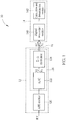
- FIG. 1 is a schematic view of a converting circuit 10 according to embodiments of the present disclosure.
- the converting circuit 10 comprises an analog circuit and a digital circuit, wherein the efficiency of the analog circuit of the converting circuit 10 is associated with the physical area of the actual circuit, and hence the analog circuit of the converting circuit 10 may be manufactured using mature processes with lower cost/unit price; whereas the digital circuit of the converting circuit 10 may be manufactured using more advanced processes or processes with smaller minimum line spacings (or minimum line widths).
- the analog circuit and the digital circuit of the electronic device 10 can be implemented on two or more than two different dies, respectively.
- the converting circuit 10 may comprise a first die 12, a second die 14 and a bus 16, wherein the first die 12 and the second die 14 are coupled (or electrically connected) to each other via the bus 16.
- the first die 12 may be manufactured using a 0.18- ⁇ m process
- the second die 14 may be manufactured using a 55-nm process.
- the first die 12 comprises primarily the analog circuit of the converting circuit 10, wherein the analog circuit comprises an analog front end (AFE) module 120 and a converting module 126.
- the converting module 126 comprises an analog-to-digital converter (ADC) 122 and a sigma-delta ( ⁇ - ⁇ ) modulator 124.
- the second die 14 comprises primarily the digital circuit of the converting circuit 10.
- the second die 14 may comprise a digital processing module140, and a calculation and determination module 142.
- the digital processing module 140 may comprise digital circuits, such as a digital filter, a digital amplifier, a digital mixer and a digital integrator, and the calculation and determination module 142 may, based on an output of the digital processing module140, perform calculation or determination operations associated with the operation of the converting circuit 10. For example, when the converting circuit 10 is applied to a touch panel, the calculation and determination module 142 can be used to determine a touch event associated with the touch panel.
- the AFE module 120 receives a signal RX, and the converting circuit 10 determines the touch event associated with the touch panel according to the signal RX, wherein the signal RX described herein is a sense signal detected by sense electrodes of the touch panel.
- a first digital signal S1 outputted by the ADC 122 may have a specification different from that of a digital signal carried by the bus 16.
- Embodiments of the present disclosure can use the sigma-delta modulator 124 in the converting module 126 to convert the specification of the first digital signal S1 into a specification applicable to the bus 16.
- the first digital signal S1 outputted by the ADC 122 may have a bit width N 1
- the bus 16 may have a bus bit width N BUS .
- bit width N 1 is greater than the bus bit width N BUS
- the sigma-delta modulator 124 may output a second digital signal S2 having the bus bit width N BUS according to the first digital signal S1 having the bit width N 1 , so as to prevent the loss of signal fidelity.
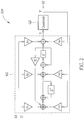
- FIG. 2 is a schematic view of a sigma-delta modulator 224 according to embodiments of the present disclosure.
- the sigma-delta modulator 224 may be used to implement the sigma-delta modulator 124 in the converting module 126, wherein a sampling rate of the ADC 122 in the converting module 126 corresponds to a Nyquist rate of the signal RX.
- the sigma-delta modulator 224 comprises a filter H2 and a quantizer Q2.
- the quantizer Q2 is an N 2 -bit quantizer, and the number of bits outputted by the quantizer Q2, or a bit number N 2 , is equal to the bus bit width N BUS (i.e.
- the filter H2 is a second-order filter.
- V ( z )and Y ( z ) represent, respectively, the z-domain signal representations corresponding to a signal outputted by the filter H2 and a signal outputted by the quantizer Q2.
- E ( z ) represents the z-domain representation of quantization noise introduced by the quantizer Q2.
- U(z) represents the z-domain representation of an input signal of the filter H2.
- the coefficient a 3 may be 0, or the system does not include the coefficient a 3 .
- the coefficients a 1 , a 2 , a 3 , b 1 , b 2 , b 3 and g may be properly designed, so that the noise frequency spectrum of the quantization noise, which is obtained by performing noise shaping on the quantization noise, falls outside the signal band rather than decreases the signal-to-noise ratio within the signal band to a relatively low level.
- the converting module 126 may use the sigma-delta modulator 224 to convert the first digital signal S1 having the bit width N 1 into a second digital signal S2 having the bit width N 2 , so as to prevent the loss of signal fidelity.
- the proposed converting module may also alter the bit rate of the first digital signal outputted by the analog-to-digital converter.
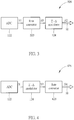
- FIG. 3 and FIG. 4 are schematic views of the converting module 326 and the converting module 426, respectively, according to embodiments of the present disclosure.
- the converting module 326 and the converting module 426 are similar to the converting module 126, and hence, the same components/elements are designated with the same reference numerals.
- the converting module 326 further comprises a rate converter 323, and the converting module 426 further comprises a rate converter 423.
- Each of the rate converters 323 and 423 is a bit rate converter, which may comprise an up-sampler or a down-sampler. Further description is provided later.
- the rate converter 323 is coupled (or electrically connected) between the ADC 122 and the sigma-delta modulator 124.
- the rate converter 323 is configured to convert the first digital signal S1 having the bit width N 1 and a bit rate r 1 into a third digital signal S3 having the bit width N 1 and a bit rate r 2 .
- the sigma-delta modulator 124 converts the third digital signal S3 having the bit width N 1 and bit rate r 2 into the second digital signal S2 having the bit width N 2 and bit rate r 2 , and outputs the second digital signal S2 to the bus 16.
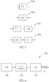
- the rate converter 423 is coupled (or electrically connected) between the sigma-delta modulator 124 and the bus 16.
- the sigma-delta modulator 124 is configured to convert the first digital signal S1 having the bit width N 1 and the bit rate r 1 into a second digital signal S2 having the bit width N 2 and the bit rate r 1 .
- the rate converter 423 converts the second digital signal S2 having the bit width N 2 and bit rate r 1 into a fourth digital signal S4 having the bit width N 2 and bit rate r 2 , and outputs the fourth digital signal S4 to the bus 16.
- each of the rate converters 523a, 523b, 523c and 523d may be used to implement the rate converter 323 and 423.
- each of the rate converters 323 and 423 may comprise a down-sampler (e.g.
- FIG. 6 is a schematic view of a converting module 626 according to embodiments of the present disclosure.
- the converting module 626 comprises an ADC 622, a sigma-delta modulator 624, and a rate converter 623.
- the ADC 622 is a sigma-delta ( ⁇ - ⁇ ) ADC; that is, the ADC 622 is an oversampling ADC.
- the sampling rate of the ADC 622 is greater than N times the Nyquist rate corresponding to the signal RX.
- N can be greater than 5.
- N can be greater than 10.
- the bit width N 2 of the signal outputted by the sigma-delta modulator may be greater or smaller than the bit width N1 of the signal outputted by the bit width N 1 depending on the signal specification of the bus.
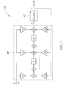
- FIG. 7 is a schematic view of a sigma-delta modulator 724 according to embodiments of the present disclosure.
- the sigma-delta modulator 724 may be used to implement the sigma-delta modulator 624 of the converting module 626, wherein the sigma-delta modulator 624 is coupled to an oversampling ADC 622 having a sampling rate greater than N times the Nyquist rate.
- the sigma-delta modulator 724 comprises a filter H7 and the N 2 -bit quantizer Q2.
- the filter H7 is a second-order filter.
- the filter H7 may effectively prevent the quantization noise of the quantizer Q2 from entering into the signal band, or prevent the quantization noise, which has been processed using the down-sampling operation, from entering the signal band.
- the filter coefficients a 1 and a 2 may be designed in such a way that a pole of the noise transfer function of the filter H7 is located in a band other than the signal band. Accordingly, the quantization noise of the quantizer Q2 can be located at the band other than the signal band.
- the filter coefficients b 1 , b 2 and b 3 may be designed in such a way that a zero of the signal transfer function of the filter H7 is located at a high frequency outside the signal band. In this way, it is feasible to prevent the quantization noise, which is introduced by the oversampling ADC 622 and undergoes the down-sampling operation, from entering the signal band.
- FIG. 8 is a schematic view of the noise frequency spectrum outputted by the converting module according to embodiments of the present disclosure.
- the curve e1 represents the noise frequency spectrum outputted by a sigma-delta ADC having a sampling rate equal to a frequency Fs/2.
- the curve e2 represents the noise frequency spectrum outputted by the converting module 626, wherein a sampling rate of the sigma-delta ADC 622 is equal to a frequency Fs, and the down-sampling rate M of the rate converter 623 is 2.
- a sampling rate of an output signal of the converting module 626 is also the frequency Fs/2.
- the noise frequency spectrum corresponding to the sigma-delta ADC having the sampling rate Fs/2 is wider.
- the noise energy entering into the signal band can be effectively reduced, thereby maintaining a better signal-to-noise ratio.
- the present disclosure uses the sigma-delta modulator to convert the bit width, and uses the rate converter to convert the bit rate, thereby solving the issue of inconsistent signal specifications in the prior art. Also, by properly designing the filter within the sigma-delta modulator to effectively suppress the noise, the present disclosure can effectively reduce the noise energy entering into the signal band, and maintain a better signal-to-noise ratio.
Landscapes
- Engineering & Computer Science (AREA)
- Theoretical Computer Science (AREA)
- Compression, Expansion, Code Conversion, And Decoders (AREA)
Abstract
Description
- The present disclosure relates to converting modules and converting circuits, and in particular, to converting modules and converting circuits capable of converting a bit width.
- An integrated circuit of an electronic product may be divided into an analog circuit and a digital circuit. As the efficiency of the analog circuit is associated with the physical area of the actual circuit, the analog circuit may be manufactured using mature processes with lower cost or unit price. On the other hand, the digital circuit may be manufactured using more advanced processes, or using processes with smaller minimum line spacings or minimum line widths. In other words, the analog circuit and the digital circuit of the electronic product can be implemented on two or more than two different dies, or bare dies, respectively. The different dies are coupled or electrically connected to each other through the bus.
- However, an output signal of some circuit modules of the die including the analog circuit, referred to as an analog die for short, may have a signal specification different from that of a signal which can be carried by the bus. In the existing art, it is necessary to modify the signal specification of the output signal of such circuit modules of the analog die so as to meet the signal specification for the bus, causing trouble and inconvenience in designing circuits. The circuit modules, besides, cannot be effectively utilized. In view of the foregoing, there is a need for improvement in the related art.
- Therefore, a main object of some embodiments of the present disclosure is to provide converting modules and converting circuits capable of converting a bit width, so as to overcome the drawbacks of the prior art.
- In order to resolve the above issues, the present disclosure provides a converting module. The first die is formed in a first die. The first die is coupled to a bus. The bus has a bus bit width. The converting module comprises an analog-to-digital converter, configured to generate a first digital signal, wherein the first digital signal has a first bit width different from the bus bit width; and a sigma-delta modulator, coupled to the analog-to-digital converter, the sigma-delta modulator configured to generate a second digital signal according to the first digital signal, wherein the second digital signal has a bit width equal to the bus bit width, the sigma-delta modulator comprises a filter and a quantizer, and a number of bits outputted by the quantizer is equal to the bus bit width.
- Preferably, the first die is coupled to a second die through the bus.
- Preferably, a sampling rate of the analog-to-digital converter is equal to a Nyquist rate, a noise transfer function of the filter is expressed as


- Preferably, a sampling rate of the analog-to-digital converter is greater than a Nyquist rate, a noise transfer function of the filter is expressed as


- Preferably, the converting module further comprises a rate converter, wherein the rate converter is coupled to the sigma-delta modulator.
- Preferably, the rate converter is coupled between the analog-to-digital converter and the sigma-delta modulator; the rate converter receives the first digital signal having a first bit rate, and converts the first digital signal into a third digital signal having a second bit rate; and the sigma-delta modulator receives the third digital signal and generates the second digital signal having the second bit rate.
- Preferably, the sigma-delta modulator receives the first digital signal and generates the second digital signal; the rate converter is coupled between the sigma-delta modulator and the bus; the rate converter receives the second digital signal, and converts the second digital signal having a first bit rate into a fourth digital signal having a second bit.
- Preferably, the rate converter is an up-sampler.
- Preferably, the rate converter is a down-sampler.
- The present disclosure further provides a converting circuit. The converting circuit comprises a bus, having a bus bit width; a first die, fabricated by a first process, wherein the first die comprises: an analog-to-digital converter, configured to generate a first digital signal, wherein the first digital signal has a first bit width different from the bus bit width; and a sigma-delta modulator, coupled to the analog-to-digital converter, the sigma-delta modulator configured to generate a second digital signal according to the first digital signal, wherein the second digital signal has a bit width equal to the bus bit width, the sigma-delta modulator comprises a filter and a quantizer, and a number of bits outputted by the quantizer is equal to the bus bit width; and a second die, fabricated by a second process, wherein the second die is coupled to the first die through the bus.
- The present disclosure uses the sigma-delta modulator to convert the bit width, uses the rate converter to convert the bit rate, and properly designs the filter within the sigma-delta modulator to suppress the noise effectively. As a result, the present disclosure can effectively reduce the noise energy within the signal band, maintain a better signal-to-noise ratio, and solve the issue of inconsistent signal specifications in the prior art.
-
-
FIG. 1 is a schematic view of a converting circuit according to one embodiment of the present disclosure. -
FIG. 2 is a schematic view of a sigma-delta modulator according to one embodiment of the present disclosure. -
FIG. 3 is a schematic view of a converting module according to one embodiment of the present disclosure. -
FIG. 4 is a schematic view of a converting module according to another embodiment of the present disclosure. -
FIG. 5 is a schematic view of a plurality of rate converters according to one embodiment of the present disclosure. -
FIG. 6 is a schematic view of a converting module according to yet another embodiment of the present disclosure. -
FIG. 7 is a schematic view of a sigma-delta modulator according to another embodiment of the present disclosure. -
FIG. 8 is a schematic view of the noise frequency spectrum outputted by the converting module according to embodiments of the present disclosure. - The detailed description provided below in connection with the appended drawings is intended as a description of the present examples so that so that those skilled in the art may better understand the purposes, technical solutions, and advantages of the present application. It should be noted that the embodiments of the present application are provided for illustrative purposes, and are not limiting.
- In the present disclosure and the claims, the term "coupled" refers to any direct or indirect means for electrical connection, whereas the term "electrically connected" refers to a direct electric connection.
- Reference is made to
FIG. 1 , which is a schematic view of a convertingcircuit 10 according to embodiments of the present disclosure. Theconverting circuit 10 comprises an analog circuit and a digital circuit, wherein the efficiency of the analog circuit of theconverting circuit 10 is associated with the physical area of the actual circuit, and hence the analog circuit of theconverting circuit 10 may be manufactured using mature processes with lower cost/unit price; whereas the digital circuit of theconverting circuit 10 may be manufactured using more advanced processes or processes with smaller minimum line spacings (or minimum line widths). In other words, the analog circuit and the digital circuit of theelectronic device 10 can be implemented on two or more than two different dies, respectively. - Specifically, the
converting circuit 10 may comprise afirst die 12, asecond die 14 and abus 16, wherein thefirst die 12 and thesecond die 14 are coupled (or electrically connected) to each other via thebus 16. In one embodiment, thefirst die 12 may be manufactured using a 0.18-µm process, whereas the second die 14 may be manufactured using a 55-nm process. Thefirst die 12 comprises primarily the analog circuit of theconverting circuit 10, wherein the analog circuit comprises an analog front end (AFE)module 120 and aconverting module 126. Theconverting module 126 comprises an analog-to-digital converter (ADC) 122 and a sigma-delta (Σ-Δ)modulator 124. Thesecond die 14 comprises primarily the digital circuit of theconverting circuit 10. In one embodiment, the second die 14 may comprise a digital processing module140, and a calculation anddetermination module 142. In one embodiment, thedigital processing module 140 may comprise digital circuits, such as a digital filter, a digital amplifier, a digital mixer and a digital integrator, and the calculation anddetermination module 142 may, based on an output of the digital processing module140, perform calculation or determination operations associated with the operation of theconverting circuit 10. For example, when theconverting circuit 10 is applied to a touch panel, the calculation anddetermination module 142 can be used to determine a touch event associated with the touch panel. In other words, theAFE module 120 receives a signal RX, and theconverting circuit 10 determines the touch event associated with the touch panel according to the signal RX, wherein the signal RX described herein is a sense signal detected by sense electrodes of the touch panel. - It should be noted that a first digital signal S1 outputted by the ADC 122 may have a specification different from that of a digital signal carried by the
bus 16. Embodiments of the present disclosure can use the sigma-delta modulator 124 in theconverting module 126 to convert the specification of the first digital signal S1 into a specification applicable to thebus 16. Specifically, the first digital signal S1 outputted by theADC 122 may have a bit width N1, whereas thebus 16 may have a bus bit width NBUS. In a case where the bit width N1 is greater than the bus bit width NBUS, if the first digital signal S1 having the bit width N1 is directly sent to thebus 16 having the bus bit width NBUS, loss of signal fidelity would occur because N1>NBUS. With the use of the sigma-delta modulator 124, the bit width N1 of the first digital signal S1 can be converted into a bit width N2 that is equal to the bus bit width NBUS (i.e. N2=NBUS). In other words, the sigma-delta modulator 124 may output a second digital signal S2 having the bus bit width NBUS according to the first digital signal S1 having the bit width N1, so as to prevent the loss of signal fidelity. - For example, reference is now made to
FIG. 2 , which is a schematic view of a sigma-delta modulator 224 according to embodiments of the present disclosure. The sigma-delta modulator 224 may be used to implement the sigma-delta modulator 124 in theconverting module 126, wherein a sampling rate of theADC 122 in theconverting module 126 corresponds to a Nyquist rate of the signal RX. The sigma-delta modulator 224 comprises a filter H2 and a quantizer Q2. The quantizer Q2 is an N2-bit quantizer, and the number of bits outputted by the quantizer Q2, or a bit number N2, is equal to the bus bit width NBUS (i.e. N2=NBUS). In the embodiment illustrated inFIG. 2 , the filter H2 is a second-order filter. Specifically, in one embodiment, the filter H2 may have a noise transfer function (NTF):

FIG. 2 , the coefficient a 3 may be 0, or the system does not include the coefficient a3. Furthermore, the coefficients a 1, a 2, a 3, b 1, b 2, b 3 and g may be properly designed, so that the noise frequency spectrum of the quantization noise, which is obtained by performing noise shaping on the quantization noise, falls outside the signal band rather than decreases the signal-to-noise ratio within the signal band to a relatively low level. - In view of the foregoing, when the bit width N1 of the first digital signal S1 outputted by the
ADC 122 is greater than the bus bit width NBUS, the convertingmodule 126 may use the sigma-delta modulator 224 to convert the first digital signal S1 having the bit width N1 into a second digital signal S2 having the bit width N2, so as to prevent the loss of signal fidelity. - Furthermore, in addition to changing the bit width of the first digital signal outputted by the analog-to-digital converter, the proposed converting module may also alter the bit rate of the first digital signal outputted by the analog-to-digital converter. Reference is made to
FIG. 3 and FIG. 4 , which are schematic views of the convertingmodule 326 and the convertingmodule 426, respectively, according to embodiments of the present disclosure. The convertingmodule 326 and the convertingmodule 426 are similar to the convertingmodule 126, and hence, the same components/elements are designated with the same reference numerals. Unlike the convertingmodule 126, the convertingmodule 326 further comprises arate converter 323, and the convertingmodule 426 further comprises arate converter 423. Each of therate converters - In the converting
module 326 illustrated inFIG. 3 , therate converter 323 is coupled (or electrically connected) between theADC 122 and the sigma-delta modulator 124. Therate converter 323 is configured to convert the first digital signal S1 having the bit width N1 and a bit rate r1 into a third digital signal S3 having the bit width N1 and a bit rate r2. Next, the sigma-delta modulator 124 converts the third digital signal S3 having the bit width N1 and bit rate r2 into the second digital signal S2 having the bit width N2 and bit rate r2, and outputs the second digital signal S2 to thebus 16. - In the converting
module 426 illustrated inFIG. 4 , therate converter 423 is coupled (or electrically connected) between the sigma-delta modulator 124 and thebus 16. The sigma-delta modulator 124 is configured to convert the first digital signal S1 having the bit width N1 and the bit rate r1 into a second digital signal S2 having the bit width N2 and the bit rate r1. Next, therate converter 423 converts the second digital signal S2 having the bit width N2 and bit rate r1 into a fourth digital signal S4 having the bit width N2 and bit rate r2, and outputs the fourth digital signal S4 to thebus 16. - Furthermore, reference is made to
FIG. 5 , which is a schematic view of therate converters rate converters rate converter rate converters rate converter 523a), thereby outputting digital signals having the bit rate r2 that is L times the bit rate r1 (i.e. r2=L×r1). In one embodiment, each of therate converters rate converter 523b), thereby outputting digital signals having the bit rate r2 that is (1/M) times the bit rate r1 (i.e. r2=r1/M). In one embodiment, therate converter e.g. rate converters - Furthermore, reference is made to
FIG. 6 , which is a schematic view of a convertingmodule 626 according to embodiments of the present disclosure. The convertingmodule 626 comprises anADC 622, a sigma-delta modulator 624, and arate converter 623. In the convertingmodule 626 illustrated inFIG. 6 , therate converter 623 is a down-sampler, wherein the down-sampling rate M of therate converter 623 may be 2 (M=2). Furthermore, theADC 622 is a sigma-delta (Σ-Δ) ADC; that is, theADC 622 is an oversampling ADC. In other words, the sampling rate of theADC 622 is greater than N times the Nyquist rate corresponding to the signal RX. N can be greater than 5. Preferably, N can be greater than 10. In this case, the bit width N2 of the signal outputted by the sigma-delta modulator may be greater or smaller than the bit width N1 of the signal outputted by the bit width N1 depending on the signal specification of the bus. When theADC 622 is the oversampling ADC, therate converter 623 is coupled to the output terminal of the sigma-delta modulator 624. In this way, it is feasible to avoid the aliasing effect associated with the noise frequency spectrum due to the down-sampling operation, and therefore, the decrease in the signal-to-noise ratio of the signal band due to the aliasing effect may be prevented. - Moreover, reference is made to
FIG. 7 , which is a schematic view of a sigma-delta modulator 724 according to embodiments of the present disclosure. The sigma-delta modulator 724 may be used to implement the sigma-delta modulator 624 of the convertingmodule 626, wherein the sigma-delta modulator 624 is coupled to anoversampling ADC 622 having a sampling rate greater than N times the Nyquist rate. The sigma-delta modulator 724 comprises a filter H7 and the N2-bit quantizer Q2. In the embodiment illustrated inFIG. 7 , the filter H7 is a second-order filter. Specifically, in one embodiment, the filter H7 may have a noise transfer function expressed as

FIG. 7 , the coefficient a 3 may be 0. - In view of the noise transfer function of the filter H7, the filter H7 has zeros at z=+1 and z= - 1; that is, the zeros of the filter H7, relative to the sampling rate, are located at a low frequency and a high frequency. In this way, the filter H7 may effectively prevent the quantization noise of the quantizer Q2 from entering into the signal band, or prevent the quantization noise, which has been processed using the down-sampling operation, from entering the signal band. In addition, the filter coefficients a 1 and a 2 may be designed in such a way that a pole of the noise transfer function of the filter H7 is located in a band other than the signal band. Accordingly, the quantization noise of the quantizer Q2 can be located at the band other than the signal band. Furthermore, the filter coefficients b 1, b 2 and b 3 may be designed in such a way that a zero of the signal transfer function of the filter H7 is located at a high frequency outside the signal band. In this way, it is feasible to prevent the quantization noise, which is introduced by the
oversampling ADC 622 and undergoes the down-sampling operation, from entering the signal band. - Specifically, reference is directed to
FIG. 8 , which is a schematic view of the noise frequency spectrum outputted by the converting module according to embodiments of the present disclosure. InFIG. 8 , the curve e1 represents the noise frequency spectrum outputted by a sigma-delta ADC having a sampling rate equal to a frequency Fs/2. In comparison, the curve e2 represents the noise frequency spectrum outputted by the convertingmodule 626, wherein a sampling rate of the sigma-delta ADC 622 is equal to a frequency Fs, and the down-sampling rate M of therate converter 623 is 2. In other words, a sampling rate of an output signal of the convertingmodule 626 is also the frequency Fs/2. As can be observed from the curve e1 and the curve e2, within the band lower than the frequency Fs/2, the noise frequency spectrum corresponding to the sigma-delta ADC having the sampling rate Fs/2 is wider. In other words, with the use of the sigma-delta modulator 624 of the convertingmodule 626 and therate converter 623 coupled to the output terminal of the sigma-delta modulator 624, the noise energy entering into the signal band can be effectively reduced, thereby maintaining a better signal-to-noise ratio. - In view of the foregoing, the present disclosure uses the sigma-delta modulator to convert the bit width, and uses the rate converter to convert the bit rate, thereby solving the issue of inconsistent signal specifications in the prior art. Also, by properly designing the filter within the sigma-delta modulator to effectively suppress the noise, the present disclosure can effectively reduce the noise energy entering into the signal band, and maintain a better signal-to-noise ratio.
- The detailed description sets forth only some of the embodiments of the present disclosure, and should not be construed to limit the scope of the present invention. Any modification, equivalent substitution and improvement within the spirits and principles of the present invention fall within the protection scope of the present disclosure.
Claims (18)
- A converting module, formed in a first die, the first die being coupled to a bus, the bus having a bus bit width, the converting module comprising:an analog-to-digital converter, configured to generate a first digital signal, wherein the first digital signal has a first bit width different from the bus bit width; anda sigma-delta modulator, coupled to the analog-to-digital converter, the sigma-delta modulator configured to generate a second digital signal according to the first digital signal, wherein the second digital signal has a bit width equal to the bus bit width, the sigma-delta modulator comprises a filter and a quantizer, and a number of bits outputted by the quantizer is equal to the bus bit width.
- The converting module of claim 1, wherein the first die is coupled to a second die through the bus.
- The converting module of claim 1, wherein a sampling rate of the analog-to-digital converter is equal to a Nyquist rate, a noise transfer function of the filter is expressed as


- The converting module of claim 1,wherein a sampling rate of the analog-to-digital converter is greater than a Nyquist rate, a noise transfer function of the filter is expressed as


- The converting module of claim 1, further comprising a rate converter, wherein the rate converter is coupled to the sigma-delta modulator.
- The converting module of claim 5, wherein the rate converter is coupled between the analog-to-digital converter and the sigma-delta modulator; the rate converter receives the first digital signal, and the first digital signal has a first bit rate; the rate converter converts the first digital signal into a third digital signal having a second bit rate, and the sigma-delta modulator receives the third digital signal and generates the second digital signal; the second digital signal has the second bit rate different from the first second bit rate.
- The converting module of claim 5, wherein the sigma-delta modulator receives the first digital signal and generates the second digital signal; the rate converter is coupled between the sigma-delta modulator and the bus; the rate converter receives the second digital signal, and converts the second digital signal into a fourth digital signal; the second digital signal has a first bit rate, and the fourth digital signal has a second bit different from the first bit rate.
- The converting module of claim 5, wherein the rate converter is an up-sampler.
- The converting module of claim 5, wherein the rate converter is a down-sampler.
- A converting circuit, comprising:a bus, having a bus bit width;a first die, fabricated by a first process, wherein the first die comprises:an analog-to-digital converter, configured to generate a first digital signal, wherein the first digital signal has a first bit width different from the bus bit width; anda sigma-delta modulator, coupled to the analog-to-digital converter, the sigma-delta modulator configured to generate a second digital signal according to the first digital signal, wherein the second digital signal has a bit width equal to the bus bit width, the sigma-delta modulator comprises a filter and a quantizer, and a number of bits outputted by the quantizer is equal to the bus bit width; anda second die, fabricated by a second process, wherein the second die is coupled to the first die through the bus.
- The converting circuit of claim 10, wherein the first die further comprises an analog front-end module, configured to generate an analog signal and send the analog signal to the analog-to-digital converter.
- The converting circuit of claim 10, wherein the analog-to-digital converter has a sampling rate equal to a Nyquist rate, a noise transfer function of the filter is expressed as


- The converting circuit of claim 10, wherein the analog-to-digital converter has a sampling rate that is greater than a Nyquist rate, a noise transfer function of the filter is expressed as


- The converting circuit of claim 10, wherein the first die further comprises a rate converter, and the rate converter is coupled to the sigma-delta modulator.
- The converting circuit of claim 14, wherein the rate converter is coupled between the analog-to-digital converter and the sigma-delta modulator; the rate converter receives the first digital signal, and the first digital signal has a first bit rate; the rate converter converts the first digital signal into a third digital signal having a second bit rate, and the sigma-delta modulator receives the third digital signal and generates the second digital signal having the second bit rate.
- The converting circuit of claim 14, wherein the sigma-delta modulator receives the first digital signal and generates the second digital signal; the rate converter is coupled between the sigma-delta modulator and the bus; the rate converter receives the second digital signal, and converts the second digital signal having a first bit rate into a fourth digital signal having a second bit.
- The converting circuit of claim 14, wherein the rate converter is an up-sampler.
- The converting circuit of claim 14, wherein the rate converter is a down-sampler.
Applications Claiming Priority (1)
| Application Number | Priority Date | Filing Date | Title |
|---|---|---|---|
| PCT/CN2017/096472 WO2019028681A1 (en) | 2017-08-08 | 2017-08-08 | Conversion module and conversion circuit |
Publications (2)
| Publication Number | Publication Date |
|---|---|
| EP3468042A1 true EP3468042A1 (en) | 2019-04-10 |
| EP3468042A4 EP3468042A4 (en) | 2019-07-24 |
Family
ID=65273117
Family Applications (1)
| Application Number | Title | Priority Date | Filing Date |
|---|---|---|---|
| EP17908100.5A Withdrawn EP3468042A4 (en) | 2017-08-08 | 2017-08-08 | CONVERSION MODULE AND CONVERSION CIRCUIT |
Country Status (4)
| Country | Link |
|---|---|
| US (1) | US10566986B2 (en) |
| EP (1) | EP3468042A4 (en) |
| CN (1) | CN109644004B (en) |
| WO (1) | WO2019028681A1 (en) |
Family Cites Families (21)
| Publication number | Priority date | Publication date | Assignee | Title |
|---|---|---|---|---|
| EP0759233A1 (en) * | 1994-05-11 | 1997-02-26 | Analog Devices, Inc. | Digital-to-digital conversion using nonuniform sample rates |
| US5731769A (en) * | 1995-12-04 | 1998-03-24 | Motorola, Inc. | Multi-rate digital filter apparatus and method for sigma-delta conversion processes |
| US7158566B2 (en) * | 2000-07-24 | 2007-01-02 | Eric Morgan Dowling | High-speed adaptive interconnect architecture with nonlinear error functions |
| US6839010B1 (en) * | 2002-12-27 | 2005-01-04 | Zilog, Inc. | Sigma-delta analog-to-digital converter with reduced quantization noise |
| US7197522B2 (en) * | 2003-03-28 | 2007-03-27 | Ess Technology, Inc. | Bi-quad digital filter configured with a bit binary rate multiplier |
| US6958717B1 (en) * | 2003-08-25 | 2005-10-25 | Analog Devices, Inc. | Method and apparatus for interconnecting analog and digital sections of A/D and D/A converters |
| GB2408858B (en) * | 2003-12-05 | 2006-11-29 | Wolfson Ltd | Word length reduction circuit |
| DE102005057768B4 (en) * | 2005-12-02 | 2012-01-12 | Xignal Technologies Ag | Time-continuous delta-sigma analog-to-digital converter |
| JP2009290455A (en) * | 2008-05-28 | 2009-12-10 | Toshiba Corp | Dem system, delta-sigma a/d converter, and receiver |
| US7978113B2 (en) * | 2009-09-10 | 2011-07-12 | National Semiconductor Corporation | Analog-to-digital converter having output data with reduced bit-width and related system and method |
| TWI398104B (en) * | 2009-12-30 | 2013-06-01 | Univ Nat Taiwan | Modulator with loop-delay compensation |
| US8665126B2 (en) * | 2010-12-08 | 2014-03-04 | National Semiconductor Corporation | ΣΔ difference-of-squares LOG-RMS to DC converter with forward and feedback paths signal squaring |
| TW201246804A (en) * | 2011-05-05 | 2012-11-16 | Univ Nat Taiwan | Delta-sigma ADC modulator with excess loop delay compensation |
| CN103701465B (en) * | 2013-12-02 | 2016-09-21 | 苏州上声电子有限公司 | A kind of digital loudspeaker system implementation method based on many bits △ Σ modulation and device |
| EP2904963B1 (en) * | 2014-02-06 | 2017-01-25 | IMEC vzw | System and method for acquisition of biopotential signals with motion artifact reduction in real time operation |
| US9401728B2 (en) * | 2014-12-16 | 2016-07-26 | Freescale Semiconductor, Inc. | Test signal generator for sigma-delta ADC |
| CN104581589B (en) * | 2014-12-31 | 2018-01-02 | 苏州上声电子有限公司 | Channel status choosing method and device based on tri-state coding |
| WO2016155825A1 (en) * | 2015-04-01 | 2016-10-06 | Epcos Ag | Sigma-delta modulator arrangement, method and control apparatus for calibrating a continuous-time sigma-delta modulator |
| US9742430B1 (en) * | 2016-08-19 | 2017-08-22 | Infineon Technologies Ag | System and method for analog to digital conversion |
| US10608852B2 (en) * | 2017-11-14 | 2020-03-31 | Cable Television Laboratories, Inc | Systems and methods for delta-sigma digitization |
| US10348326B2 (en) * | 2017-10-23 | 2019-07-09 | Infineon Technologies Ag | Digital silicon microphone with interpolation |
-
2017
- 2017-08-08 CN CN201780000892.7A patent/CN109644004B/en not_active Expired - Fee Related
- 2017-08-08 WO PCT/CN2017/096472 patent/WO2019028681A1/en not_active Ceased
- 2017-08-08 EP EP17908100.5A patent/EP3468042A4/en not_active Withdrawn
-
2018
- 2018-11-02 US US16/179,405 patent/US10566986B2/en not_active Expired - Fee Related
Also Published As
| Publication number | Publication date |
|---|---|
| CN109644004B (en) | 2023-05-26 |
| WO2019028681A1 (en) | 2019-02-14 |
| CN109644004A (en) | 2019-04-16 |
| US20190074843A1 (en) | 2019-03-07 |
| US10566986B2 (en) | 2020-02-18 |
| EP3468042A4 (en) | 2019-07-24 |
Similar Documents
| Publication | Publication Date | Title |
|---|---|---|
| CN107852164B (en) | Suppressing Signal Transfer Function Peaking in Feedforward ΔΣ Converters | |
| US9178529B2 (en) | Multi-stage noise shaping analog-to-digital converter | |
| EP2930850B1 (en) | Cancellation of feedback digital-to-analog converter errors in multi-stage delta-sigma analog-to-digital converters | |
| US10171102B1 (en) | Oversampled continuous-time pipeline ADC with voltage-mode summation | |
| EP2273682A1 (en) | Integrator, resonator, and oversampling a/d converter | |
| CN102420614A (en) | Sigma-Delta Modulator and Sigma-Delta Analog-to-Digital Converter Containing It | |
| US9054731B2 (en) | Integrator output swing reduction | |
| CN103825618A (en) | Delta-sigma modulator and delta-sigma modulation method | |
| US10181860B1 (en) | Reducing residue signals in analog-to-digital converters | |
| US20040130471A1 (en) | Delta-Sigma modulator for reducing quantization noise and oversampling ratio (OSR) | |
| CN101971502A (en) | Multi-bit sigma-delta modulator with reduced number of bits in the feedback path | |
| CN103944575A (en) | Oversampling 64-time sigma-delta modulation circuit with effective bit being 18 | |
| CN103457574A (en) | Low-consumption digital decimation filter bank with variable decimation multiples and digital decimation and filtering method | |
| CN111900992A (en) | Analog-digital converter based on incremental modulation | |
| CN103326728B (en) | A kind of noise suppressed strengthens sigma Delta modulator structure | |
| CN114900189A (en) | MASH delta-sigma modulator with low noise leakage | |
| WO2011031995A2 (en) | Analog-to-digital converter having output data with reduced bit-width and related system and method | |
| US8405535B1 (en) | Integrated circuit with configurable analog to digital converter | |
| KR102441025B1 (en) | Semiconductor device and operating method thereof | |
| US9391634B1 (en) | Systems and methods of low power decimation filter for sigma delta ADC | |
| US9985645B2 (en) | Techniques for improving mismatch shaping of dynamic element matching circuit within delta-sigma modulator | |
| US9954514B2 (en) | Output range for interpolation architectures employing a cascaded integrator-comb (CIC) filter with a multiplier | |
| KR102081913B1 (en) | Delta-sigma modulator and analog-to-digital converter including the same | |
| US10566986B2 (en) | Converting module and converting circuit | |
| CN108832931B (en) | Delta-Sigma Modulator Using Externally Dithered Signal |
Legal Events
| Date | Code | Title | Description |
|---|---|---|---|
| STAA | Information on the status of an ep patent application or granted ep patent |
Free format text: STATUS: UNKNOWN |
|
| STAA | Information on the status of an ep patent application or granted ep patent |
Free format text: STATUS: THE INTERNATIONAL PUBLICATION HAS BEEN MADE |
|
| PUAI | Public reference made under article 153(3) epc to a published international application that has entered the european phase |
Free format text: ORIGINAL CODE: 0009012 |
|
| STAA | Information on the status of an ep patent application or granted ep patent |
Free format text: STATUS: REQUEST FOR EXAMINATION WAS MADE |
|
| 17P | Request for examination filed |
Effective date: 20181107 |
|
| AK | Designated contracting states |
Kind code of ref document: A1 Designated state(s): AL AT BE BG CH CY CZ DE DK EE ES FI FR GB GR HR HU IE IS IT LI LT LU LV MC MK MT NL NO PL PT RO RS SE SI SK SM TR |
|
| AX | Request for extension of the european patent |
Extension state: BA ME |
|
| A4 | Supplementary search report drawn up and despatched |
Effective date: 20190625 |
|
| RIC1 | Information provided on ipc code assigned before grant |
Ipc: H03M 1/08 20060101AFI20190618BHEP Ipc: H03M 3/00 20060101ALI20190618BHEP |
|
| DAV | Request for validation of the european patent (deleted) | ||
| DAX | Request for extension of the european patent (deleted) | ||
| STAA | Information on the status of an ep patent application or granted ep patent |
Free format text: STATUS: EXAMINATION IS IN PROGRESS |
|
| 17Q | First examination report despatched |
Effective date: 20210910 |
|
| STAA | Information on the status of an ep patent application or granted ep patent |
Free format text: STATUS: THE APPLICATION IS DEEMED TO BE WITHDRAWN |
|
| 18D | Application deemed to be withdrawn |
Effective date: 20240301 |