EP3467889A1 - Thermoelectric conversion device and manufacturing method for same - Google Patents
Thermoelectric conversion device and manufacturing method for same Download PDFInfo
- Publication number
- EP3467889A1 EP3467889A1 EP17802861.9A EP17802861A EP3467889A1 EP 3467889 A1 EP3467889 A1 EP 3467889A1 EP 17802861 A EP17802861 A EP 17802861A EP 3467889 A1 EP3467889 A1 EP 3467889A1
- Authority
- EP
- European Patent Office
- Prior art keywords
- insulator
- via holes
- conductive paste
- mask
- holes
- Prior art date
- Legal status (The legal status is an assumption and is not a legal conclusion. Google has not performed a legal analysis and makes no representation as to the accuracy of the status listed.)
- Withdrawn
Links
Images





Classifications
-
- H—ELECTRICITY
- H10—SEMICONDUCTOR DEVICES; ELECTRIC SOLID-STATE DEVICES NOT OTHERWISE PROVIDED FOR
- H10N—ELECTRIC SOLID-STATE DEVICES NOT OTHERWISE PROVIDED FOR
- H10N10/00—Thermoelectric devices comprising a junction of dissimilar materials, i.e. devices exhibiting Seebeck or Peltier effects
- H10N10/01—Manufacture or treatment
-
- H—ELECTRICITY
- H10—SEMICONDUCTOR DEVICES; ELECTRIC SOLID-STATE DEVICES NOT OTHERWISE PROVIDED FOR
- H10N—ELECTRIC SOLID-STATE DEVICES NOT OTHERWISE PROVIDED FOR
- H10N10/00—Thermoelectric devices comprising a junction of dissimilar materials, i.e. devices exhibiting Seebeck or Peltier effects
- H10N10/10—Thermoelectric devices comprising a junction of dissimilar materials, i.e. devices exhibiting Seebeck or Peltier effects operating with only the Peltier or Seebeck effects
- H10N10/17—Thermoelectric devices comprising a junction of dissimilar materials, i.e. devices exhibiting Seebeck or Peltier effects operating with only the Peltier or Seebeck effects characterised by the structure or configuration of the cell or thermocouple forming the device
-
- H—ELECTRICITY
- H10—SEMICONDUCTOR DEVICES; ELECTRIC SOLID-STATE DEVICES NOT OTHERWISE PROVIDED FOR
- H10N—ELECTRIC SOLID-STATE DEVICES NOT OTHERWISE PROVIDED FOR
- H10N10/00—Thermoelectric devices comprising a junction of dissimilar materials, i.e. devices exhibiting Seebeck or Peltier effects
- H10N10/80—Constructional details
- H10N10/81—Structural details of the junction
-
- H—ELECTRICITY
- H10—SEMICONDUCTOR DEVICES; ELECTRIC SOLID-STATE DEVICES NOT OTHERWISE PROVIDED FOR
- H10W—GENERIC PACKAGES, INTERCONNECTIONS, CONNECTORS OR OTHER CONSTRUCTIONAL DETAILS OF DEVICES COVERED BY CLASS H10
- H10W20/00—Interconnections in chips, wafers or substrates
- H10W20/01—Manufacture or treatment
- H10W20/031—Manufacture or treatment of conductive parts of the interconnections
- H10W20/056—Manufacture or treatment of conductive parts of the interconnections by filling conductive material into holes, grooves or trenches
Definitions
- thermoelectric conversion device relates to a thermoelectric conversion device and a method of manufacturing the same.
- thermoelectric conversion device has a thin plate-like shape, and outputs a signal in accordance with the heat flux that flows between one surface and the other surface in the thickness direction.
- a method of manufacturing such a thermoelectric conversion device is described in PTL 1.
- thermoelectric conversion device described in PTL 1
- a plurality of via holes and a plurality of voids are provided in an insulating base material including a thermoplastic resin.
- the plurality of via holes are filled with conductive pastes containing alloy powder and an organic solvent.
- a front surface protection member having front surface wiring patterns in contact with ends of the plurality of conductive pastes is arranged on one surface of the insulating base material.
- a rear surface protection member having rear surface wiring patterns in contact with the other ends of the plurality of conductive pastes is arranged on the other surface of the insulating base material so that a stacked body is formed.
- an integrating step of heating the stacked body while pressing it in the stacking direction is performed using a vacuum pressing machine.
- the conductive pastes are solid-phase sintered through the integrating step, and a plurality of conductors are formed.
- the conductors, the front surface wiring patterns, and the rear surface wiring patterns are electrically connected to each other, and the insulating base material, the front surface protection member, and the rear surface protection member are bonded together under pressure.
- thermoplastic resin that constitutes the insulating base material flows into the voids when the above-mentioned integrating step is performed, which reduces the thickness of the insulating base material. Consequently, loads are efficiently applied from the pressing machine to the conductive pastes. Therefore, with this manufacturing method, the conductive pastes can be solid-phase sintered to form conductors, and the conductors, the front surface wiring patterns, and the rear surface wiring patterns can be electrically connected to each other.
- the insulating base material used for the manufacturing method described in PTL 1 includes a thermoplastic resin that can flow into the voids by being heated in the integrating step.
- a thermoplastic resin with a melting point lower than the temperature for heating in the integrating step is used as a resin for the insulating base material. Therefore, the thermoelectric conversion device manufactured with this manufacturing method is difficult to use at temperatures higher than the melting point of the thermoplastic resin.
- the insulating base material is formed of a thermoplastic resin with a high melting point that hardly flows or of a thermosetting resin, the thickness of the insulating base material is not reduced in the integrating step. Therefore, it is difficult to efficiently apply loads from the pressing machine to the conductive pastes with the conventional manufacturing method. Thus, the development of a new method of manufacturing a thermoelectric conversion device is required.
- a method of manufacturing a thermoelectric conversion device as an aspect of the technique of the present disclosure includes first, second, and third forming steps, first and second filling steps, an arranging step, first and second preparing steps, and a pressure bonding step.
- the first forming step (S10) includes preparing a first insulator (11) having a plate-like shape and forming first and second via holes (101, 102) in the first insulator.
- the second forming step (S20) includes preparing a second insulator (12) having a plate-like shape and forming third and fourth via holes (103, 104) in the second insulator.
- the first filling step (S30) includes filling the first via holes with a first conductive paste (131) containing alloy powder and a solvent such that the first conductive paste protrudes from the first via holes by an amount larger than the thickness of the second insulator.
- the second filling step (S40) includes filling the third via holes with a second conductive paste (141) containing alloy powder and a solvent different from those of the first conductive paste such that the second conductive paste protrudes from the third via holes by an amount larger than the thickness of the first insulator.
- the arranging step (S50) includes arranging the first insulator and the second insulator such that parts of the first conductive paste protruding from the first via holes of the first insulator face the fourth via holes of the second insulator and parts of the second conductive paste protruding from the third via holes of the second insulator face the second via holes of the first insulator.
- the first preparing step (S60) includes preparing a front surface protection member (110) having front surface wiring patterns (111) connectable to the ends of the first conductive paste of the first insulator that do not face the second insulator and connectable to the ends of the second conductive paste protruding from the third via holes of the second insulator.
- the second preparing step (S70) includes preparing a rear surface protection member (120) having rear surface wiring patterns (121) connectable to the other ends of the first conductive paste protruding from the first via holes of the first insulator and connectable to the other ends of the second conductive paste of the second insulator that do not face the first insulator.
- the third forming step (S80) includes inserting the parts of the first conductive paste protruding from the first via holes into the fourth via holes, and inserting the parts of the second conductive paste protruding from the third via holes into the second via holes.
- the third forming step further includes arranging the front surface protection member having the front surface wiring patterns on the first insulator such that the front surface protection member does not face the second insulator, and arranging the rear surface protection member having the rear surface wiring patterns on the second insulator such that the rear surface protection member does not face the first insulator, thereby forming a stacked body.
- the pressure bonding step (S90) includes forming first and second conductors by heating the stacked body while pressing the stacked body in the stacking direction and by solid-phase sintering of the first and the second conductive pastes.
- the pressure bonding step further includes electrically connecting the first conductor, the second conductor, the front surface wiring patterns, and the rear surface wiring patterns, and bonding the first insulator, the second insulator, the front surface protection member, and the rear surface protection member together under pressure.
- thermoelectric conversion device in the state where the first and second insulators and the like are stacked, the first conductive paste protrudes from the second insulator toward the rear surface protection member, and the second conductive paste protrudes from the first insulator toward the front surface protection member.
- the stacked body is heated while being pressed in the stacking direction, and loads are efficiently applied from the front and rear surface wiring patterns to the first and second conductive pastes. Therefore, the first and second conductive pastes are solid-phase sintered, and become the first and second conductors, respectively.
- each of the first and second insulators can be formed using a thermoplastic resin with a high melting point or a thermosetting resin. As a result, a thermoelectric conversion device with high heat resistance can be manufactured.
- thermoelectric conversion device as an aspect of the technique of the present disclosure includes a first insulator (11), a second insulator (12), a plurality of first conductors (130), a plurality of second conductors (140), front surface wiring patterns (111), rear surface wiring patterns (121), a front surface protection member (110), and a rear surface protection member (120).
- the first insulator has a plate-like shape and has first and second via holes (101, 102).
- the second insulator has a plate-like shape and has third via holes (103) whose internal width is smaller than that of the second via holes and fourth via holes (104) whose internal width is larger than that of the first via holes.
- the second insulator is stacked on the first insulator in its thickness direction.
- the plurality of first conductors are embedded in the first via holes of the first insulator and the fourth via holes of the second insulator and have a certain thermopower (first thermopower).
- the plurality of second conductors are embedded in the second via holes of the first insulator and the third via holes of the second insulator and have a thermopower (second thermopower) different from that of the first conductors.
- the front surface wiring patterns are connected, in the first insulator, to the ends of the first conductors that do not face the second insulator and to the ends of the second conductors.
- the rear surface wiring patterns are connected, in the second insulator, to the other ends of the first conductors that do not face the first insulator and to the other ends of the second conductors.
- the front surface protection member covers the surface of the first insulator that does not face the second insulator and the front surface wiring patterns.
- the rear surface protection member covers the surface of the second insulator that does not face the first insulator and the rear surface wiring patterns.
- thermoelectric conversion device can be manufactured using the above-mentioned manufacturing method. As a result, the thermoelectric conversion device with high heat resistance can be obtained.
- thermoelectric conversion device 10 integrally includes a first insulator 11, a second insulator 12, a front surface protection member 110, and a rear surface protection member 120.
- the thermoelectric conversion device 10 includes a plurality of interlayer connection members 130 and 140 embedded therein, and the plurality of interlayer connection members 130 and 140 are alternately connected in series by front surface wiring patterns 111 and rear surface wiring patterns 121.
- the interlayer connection members 130 and 140 in the present embodiment correspond to "conductors".
- the front surface protection member 110 is regarded as transparent or translucent, and the positions of the plurality of front surface wiring patterns 111 are indicated by solid lines.
- the interlayer connection members 130 and 140 are hatched with broken lines, and the outer peripheries thereof are indicated by broken lines.
- thermoelectric conversion device 10 First, a method of manufacturing the thermoelectric conversion device 10 will be described.
- the first insulator 11 includes a flexible resin film and has a plate-like shape.
- the first insulator 11 is configured as follows using the method of manufacturing the thermoelectric conversion device 10 described later.
- the first insulator 11 includes a thermoplastic resin with a melting point higher than the temperature for solid-phase sintering first and second conductive pastes 131 and 141 (refer to FIG. 15 , etc.) or a thermosetting resin.
- the resin contained in the first insulator 11 can be, for example, an aramid resin with an adhesive layer.
- the first insulator 11 has a plurality of first and second via holes 101 and 102 extending in the thickness direction.
- the first via holes 101 and the second via holes 102 are alternately provided in the surface direction of the first insulator 11.
- the second insulator 12 includes a flexible resin film and has a plate-like shape in the same manner as the first insulator 11.
- the second insulator 12 is stacked on the first insulator 11 in its thickness direction.
- the second insulator 12 includes a thermoplastic resin with a melting point higher than the temperature for solid-phase sintering of the first and second conductive pastes 131 and 141 (described later) or a thermosetting resin.
- the resin contained in the second insulator 12 can be, for example, an aramid resin with an adhesive layer.
- the second insulator 12 has a plurality of third and fourth via holes 103 and 104 extending in the thickness direction.
- the third via holes 103 and the fourth via holes 104 are alternately provided in the surface direction of the second insulator 12.
- the third via holes 103 of the second insulator 12 are provided at positions corresponding to the second via holes 102 of the first insulator 11.
- the fourth via holes 104 of the second insulator 12 are provided at positions corresponding to the first via holes 101 of the first insulator 11.
- the internal width of the fourth via holes 104 of the second insulator 12 is larger than the internal width of the first via holes 101 of the first insulator 11.
- the internal width of the second via holes 102 of the first insulator 11 is larger than the internal width of the third via holes 103 of the second insulator 12. Note that the internal width of the first via holes 101 of the first insulator 11 is substantially equal to the internal width of the third via holes 103 of the second insulator 12.
- the internal width of the second via holes 102 of the first insulator 11 is substantially equal to the internal width of the fourth via holes 104 of the second insulator 12.
- a plurality of first interlayer connection members 130 are embedded in the first via holes 101 of the first insulator 11 and the fourth via holes 104 of the second insulator 12.
- a plurality of second interlayer connection members 140 are embedded in the second via holes 102 of the first insulator 11 and the third via holes 103 of the second insulator 12.
- the first interlayer connection members 130 and the second interlayer connection members 140 include thermoelectric materials such as metals and semiconductors having different thermopowers so as to exhibit the Seebeck effect.
- the first interlayer connection members 130 each include a metallic compound that contains solid-phase sintered p-type Bi-Sb-Te alloy powder so as to maintain the original crystal structure of a plurality of metallic atoms.
- the second interlayer connection members 140 each include a metallic compound that contains solid-phase sintered n-type Bi-Te alloy powder so as to maintain the original crystal structure of a plurality of metallic atoms.
- the surface of the first insulator 11 that does not face the second insulator 12 is covered with the front surface protection member 110 provided with the front surface wiring patterns 111.
- the front surface protection member 110 covers the surface of the first insulator 11 that does not face the second insulator 12 and the front surface wiring patterns 111.
- the front surface protection member 110 includes a flexible resin film and has a plate-like shape in the same manner as the first insulator 11.
- the front surface protection member 110 includes a thermoplastic resin with a melting point higher than the temperature for solid-phase sintering of the first and second conductive pastes 131 and 141 (described later) or a thermosetting resin.
- the resin contained in the front surface protection member 110 can be, for example, an aramid resin with an adhesive layer.
- the front surface wiring patterns 111 are patterned using copper foil or the like, and provided on the surface of the front surface protection member 110.
- the plurality of front surface wiring patterns 111 are electrically connected, in the first insulator 11, to the ends of the first interlayer connection members 130 that do not face the second insulator 12 and to the ends of the second interlayer connection members 140 adjacent thereto.
- the surface of the second insulator 12 that does not face the first insulator 11 is covered with the rear surface protection member 120 provided with the rear surface wiring patterns 121.
- the rear surface protection member 120 covers the surface of the second insulator 12 that does not face the first insulator 11 and the rear surface wiring patterns 121.
- the rear surface protection member 120 includes a flexible resin film and has a plate-like shape in the same manner as the first insulator 11.
- the rear surface protection member 120 includes a thermoplastic resin with a melting point higher than the temperature for solid-phase sintering of the first and second conductive pastes 131 and 141 (described later) or a thermosetting resin.
- the resin contained in the rear surface protection member 120 can be, for example, an aramid resin with an adhesive layer.
- the rear surface wiring patterns 121 are patterned using copper foil or the like, and provided on the surface of the rear surface protection member 120.
- the plurality of rear surface wiring patterns 121 are electrically connected, in the second insulator 12, to the other ends of the first interlayer connection members 130 that do not face the first insulator 11 and to the other ends of the second interlayer connection members 140 adjacent thereto.
- the first and second interlayer connection members 130 and 140 adjacent to each other are connected by the front and rear surface wiring patterns 111 and 121 in an alternate folding manner. In this manner, the first and second interlayer connection members 130 and 140 are connected in series by the front and rear surface wiring patterns 111 and 121. Note that the ends of the front surface wiring patterns 111 or rear surface wiring patterns 121 that connect the first and second interlayer connection members 130 and 140 in series are directly exposed to outside air. Alternatively, the ends of the front surface wiring patterns 111 or rear surface wiring patterns 121 are exposed to outside air through metal members (not illustrated) or the like. The exposed parts serve as electrical connections between the thermoelectric conversion device 10 and an external detection device (not illustrated).
- thermoelectric conversion device 10 outputs the generated thermoelectric force as a sensor signal (e.g., voltage signal).
- thermoelectric conversion device 10 Next, a method of manufacturing the thermoelectric conversion device 10 will be described.
- the manufacturing method according to the present embodiment includes a first insulator preparing step (S10), a second insulator preparing step (S20), a first conductive paste filling step (S30), and a second conductive paste filling step (S40).
- the manufacturing method according to the present embodiment also includes an insulator arranging step (S50), a front surface protection member preparing step (S60), a rear surface protection member preparing step (S70), a stacked body forming step (S80), and an integrating step (S90).
- the first insulator preparing step (S10) the above-mentioned first insulator 11 is prepared. Then, drill working, laser working, or the like is performed on the prepared first insulator 11. Consequently, the first via holes 101 and the second via holes 102 are formed in the first insulator preparing step (S10).
- the first insulator preparing step (S10) in the present embodiment corresponds to a "first forming step".
- the second insulator preparing step (S20) the above-mentioned second insulator 12 is prepared. Then, drill working, laser working, or the like is performed on the prepared second insulator 12. Consequently, the third via holes 103 and the fourth via holes 104 are formed in the second insulator preparing step (S20).
- the second insulator preparing step (S20) in the present embodiment corresponds to a "second forming step".
- the internal width of the fourth via holes 104 of the second insulator 12 is larger than the internal width of the first via holes 101 of the first insulator 11.
- the internal width of the second via holes 102 of the first insulator 11 is larger than the internal width of the third via holes 103 of the second insulator 12.
- thermoelectric conversion device 10 Next, the first conductive paste filling step S30 of the method of manufacturing the thermoelectric conversion device 10 will be described.
- the first conductive paste filling step (S30) is the step of filling the first via holes 101 of the first insulator 11 with the first conductive paste 131.
- the first conductive paste filling step (S30) in the present embodiment corresponds to a "first filling step".
- the first conductive paste filling step (S30) includes a first mask providing step (S31), a first conductive paste supplying step (S32), a first conductive paste collecting step (S33), a first mask peeling step (S34), and the like.
- the conductive material filling device described in JP 2010-50356 A can be used as a device for performing the first conductive paste filling step (S30).
- the following members are arranged on an adsorbing metal plate 20 of a conductive material filling device (not illustrated) as illustrated in FIG. 6 .
- adsorbing paper 21, the first insulator 11, a first mask 22, and a first metal mask 23 are arranged on the adsorbing metal plate 20 in this order.
- a plurality of holes 24 are provided in the adsorbing metal plate 20.
- the space below the plurality of holes 24 is connected to a vacuum pump (not illustrated).
- the adsorbing metal plate 20 is heated by a heater (not illustrated).
- the adsorbing paper 21 arranged on the adsorbing metal plate 20 can be any material that absorbs solvents used for the conductive pastes 131 and 141 (described later).
- commonly available high-quality paper is used as the adsorbing paper 21.
- the first insulator 11 including the first and second via holes 101 and 102 is arranged on the adsorbing paper 21.
- the first mask 22 is arranged on the first insulator 11.
- the thickness of the first mask 22 is larger than the thickness of the second insulator 12.
- the first mask 22 has first mask holes 25 at positions corresponding to the first via holes 101.
- the capacity of the first mask holes 25 is larger than the capacity of the fourth via holes 104 of the second insulator 12.
- the material for the first mask 22 can be, for example, an aramid resin.
- the first metal mask 23 is arranged on the first mask 22.
- the first metal mask 23 may have any thickness as long as the first metal mask 23 is rigid enough to withstand the friction of a filling squeegee in the first conductive paste supplying step (S32) described later.
- the first metal mask 23 has first metal mask holes 26 at positions corresponding to the first mask holes 25. Consequently, in the first mask providing step (S31), the adsorbing paper 21, the first insulator 11, the first mask 22, and the first metal mask 23 are arranged on the adsorbing metal plate 20 in this order.
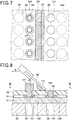
- a filling squeegee 27 is moved in the direction of arrow A on the first metal mask 23 as illustrated in FIGS. 6 and 7 .
- the first conductive paste 131 is discharged from the filling squeegee 27.
- a rear end 271 of the filling squeegee 27 relative to its moving direction is moved in contact with the upper surface of the first metal mask 23. Consequently, the first conductive paste 131 is rubbed into the first via holes 101 through the first metal mask holes 26 and the first mask holes 25 from above the first metal mask 23. Note that any excess first conductive paste 131 is rubbed off using the end 271 of the filling squeegee 27.
- the first conductive paste 131 can be made, for example, by adding Bi-Sb-Te alloy fine powder whose metallic atoms maintain a certain crystal structure to an organic solvent such as paraffin so that a paste is obtained.
- the first conductive paste supplying step (S32) the first insulator 11, the first mask 22, and the first metal mask 23 are heated by the above-mentioned heater to a temperature higher than the melting point of the organic solvent contained in the first conductive paste 131. Consequently, in the first conductive paste supplying step (S32), the first conductive paste 131 is supplied into the first metal mask holes 26, the first mask holes 25, and the first via holes 101 with its organic solvent melted.
- the first metal mask holes 26, the first mask holes 25, and the first via holes 101 are evacuated by the above-mentioned vacuum pump. Consequently, in the first conductive paste supplying step (S32), no voids are included in the first conductive paste 131 within the first metal mask holes 26, the first mask holes 25, and the first via holes 101.
- the first conductive paste supplying step (S32) most of the organic solvent contained in the first conductive paste 131 supply into the first metal mask holes 26, the first mask holes 25, and the first via holes 101 is adsorbed by the adsorbing paper 21. Therefore, in the first conductive paste supplying step (S32), the first conductive paste 131 is supplied into the first metal mask holes 26, the first mask holes 25, and the first via holes 101 from above the first metal mask 23, with its alloy fine powder densely packed.
- the first metal mask 23 is removed from the upper surface of the first mask 22 as illustrated in FIGS. 8 and 9 . Consequently, the first conductive paste 131 within the first metal mask holes 26 protrudes from the upper surface of the first mask 22.
- a metal squeegee 28 is moved in the direction of arrow B on the first mask 22. Then, the first conductive paste 131 protruding from the first mask 22 is scraped off.
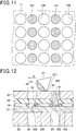
- the first mask 22 is removed from the first insulator 11 as illustrated in FIGS. 10 and 11 . Consequently, the first conductive paste 131 within the first via holes 101 of the first insulator 11 protrudes from the first via holes 101 by the thickness of the first mask 22.
- the thickness of the first mask 22 is larger than the thickness of the second insulator 12. Therefore, the first conductive paste 131 protrudes from the first via holes 101 by an amount larger than the thickness of the second insulator 12.
- the capacity of the first mask holes 25 of the first mask 22 is larger than the capacity of the fourth via holes 104 of the second insulator 12. Therefore, the volume of the parts of the first conductive paste 131 protruding from the first via holes 101 is larger than the capacity of the fourth via holes 104 of the second insulator 12.
- the second conductive paste filling step (S40) is the step of filling the second via holes 102 of the second insulator 12 with the second conductive paste 141.
- the second conductive paste filling step (S40) in the present embodiment corresponds to a "second filling step".
- the second conductive paste filling step (S40) includes a second mask providing step (S41), a second conductive paste supplying step (S42), a second conductive paste collecting step (S43), a second mask peeling step (S44), and the like.
- the following members are arranged on the adsorbing metal plate 20 of the conductive material filling device as illustrated in FIG. 12 .
- the adsorbing paper 21, the second insulator 12, a second mask 29, and a second metal mask 30 are arranged on the adsorbing metal plate 20 in this order.
- the thickness of the second mask 29 arranged on the second insulator 12 is larger than the thickness of the first insulator 11.
- the second mask 29 has second mask holes 31 at positions corresponding to the third via holes 103.
- the capacity of the second mask holes 31 is larger than the capacity of the second via holes 102 of the first insulator 11.
- the material for the second mask 29 can be, for example, an aramid resin.
- the second metal mask 30 arranged on the second mask 29 has second metal mask holes 32 at positions corresponding to the second mask holes 31.
- the second conductive paste supplying step (S42) the above-mentioned heater and vacuum pump are driven, and the filling squeegee 27 is moved in the direction of arrow C on the second metal mask 30 as illustrated in FIG. 12 . Then, the second conductive paste 141 is discharged from the filling squeegee 27.
- the second conductive paste 141 can be made, for example, by adding Bi-Te alloy fine powder whose metallic atoms maintain a certain crystal structure to an organic solvent such as paraffin so that a paste is obtained.
- the second conductive paste supplying step (S42) most of the organic solvent contained in the second conductive paste 141 supply into the second metal mask holes 32, the second mask holes 31, and the third via holes 103 is adsorbed by the adsorbing paper 21. Therefore, in the second conductive paste supplying step (S42), the second conductive paste 141 is supplied into the second metal mask holes 32, the second mask holes 31, and the third via holes 103 from above the second metal mask 30, with its alloy fine powder densely packed.
- the second metal mask 30 is removed from the upper surface of the second mask 29 as illustrated in FIG. 13 . Consequently, the second conductive paste 141 within the second metal mask holes 32 protrudes from the upper surface of the second mask 29.
- the metal squeegee 28 is moved in the direction of arrow D on the second mask 29. Then, the second conductive paste 141 protruding from the second mask 29 is scraped off.
- the second mask 29 is removed from the second insulator 12 as illustrated in FIG. 14 . Consequently, the second conductive paste 141 within the third via holes 103 of the second insulator 12 protrudes from the third via holes 103 by the thickness of the second mask 29.
- the thickness of the second mask 29 is larger than the thickness of the first insulator 11. Therefore, the second conductive paste 141 protrudes from the third via holes 103 by an amount larger than the thickness of the first insulator 11.
- the capacity of the second mask holes 31 of the second mask 29 is larger than the capacity of the second via holes 102 of the first insulator 11. Therefore, the volume of the parts of the second conductive paste 141 protruding from the third via holes 103 is larger than the capacity of the second via holes 102 of the first insulator 11.
- thermoelectric conversion device 10 Next, the insulator arranging step (S50) of the method of manufacturing the thermoelectric conversion device 10 will be described.
- the first insulator 11 is arranged such that the parts of the first conductive paste 131 protruding from the first via holes 101 face the fourth via holes 104 of the second insulator 12 as illustrated in FIG. 15 .
- the second insulator 12 is arranged such that the parts of the second conductive paste 141 protruding from the third via holes 103 face the second via holes 102 of the first insulator 11.
- the front surface protection member 110 having the front surface wiring patterns 111 is prepared as illustrated in FIG. 15 .
- the front surface wiring patterns 111 are arranged in the above-mentioned insulator arranging step (S50) in the following manner. Specifically, the front surface wiring patterns 111 are arranged at positions where they are connectable to the ends of the first conductive paste 131 of the first insulator 11 that do not face the second insulator 12 and connectable to the ends of the second conductive paste 141 protruding from the third via holes 103 of the second insulator 12.
- the method of manufacturing the front surface wiring patterns 111 and the front surface protection member 110 first includes forming copper foil or the like on at least the surface of the front surface protection member 110 that faces the first insulator 11. The method further includes patterning the copper foil appropriately. The front surface wiring patterns 111 are formed on the front surface protection member 110 with this method.
- the rear surface protection member 120 having the rear surface wiring patterns 121 is prepared.
- the rear surface wiring patterns 121 are arranged in the above-mentioned insulator arranging step (S50) in the following manner. Specifically, the rear surface wiring patterns 121 are arranged at positions where they are connectable to the other ends of the first conductive paste 131 protruding from the first via holes 101 of the first insulator 11 and connectable to the other ends of the second conductive paste 141 of the second insulator 12 that do not face the first insulator 11.
- the method of manufacturing the rear surface wiring patterns 121 and the rear surface protection member 120 first includes forming copper foil or the like on at least the surface of the rear surface protection member 120 that faces the second insulator 12. The method further includes patterning the copper foil appropriately.
- the rear surface wiring patterns 121 are formed on the rear surface protection member 120 with this method.
- the following members are arranged on a lower pressing plate 40 of a pressing machine as illustrated in FIG. 16 .
- a lower buffer 41, lower release paper 42, the rear surface protection member 120, the second insulator 12, the first insulator 11, the front surface protection member 110, upper release paper 43, and an upper buffer 44 are arranged on the lower pressing plate 40 in this order.
- the lower buffer 41 and the upper buffer 44 can be, for example, Teflon (registered trademark).
- the lower release paper 42 and the upper release paper 43 can be, for example, resin sheets formed of an aramid resin or the like.
- the parts of the first conductive paste 131 protruding from the first via holes 101 of the first insulator 11 are inserted into the fourth via holes 104.
- the parts of the second conductive paste 141 protruding from the third via holes 103 of the second insulator 12 are inserted into the second via holes 102.
- the front surface protection member 110 is arranged such that the front surface wiring patterns 111 face the surface of the first insulator 11 that does not face the second insulator 12.
- the rear surface protection member 120 is arranged such that the rear surface wiring patterns 121 face the surface of the second insulator 12 that does not face the first insulator 11. Consequently, a stacked body is formed.
- the integrating step (S90) the stacked body arranged between the lower pressing plate 40 and an upper pressing plate 47 of the pressing machine illustrated in FIG. 16 is heated while being pressed in the stacking direction in a vacuum.
- the integrating step (S90) includes a degassing step, a press molding step, a cooling step, and the like as illustrated in FIG. 17 .
- the pressure (press pressure) applied to the stacked body and the temperature for heating the stacked body in the integrating step (S90) are indicated by solid line P and broken line Q, respectively.
- the degassing step is performed during the period from time T0 to time T1 (for example, for 600 seconds).
- evacuation is performed with the vacuum pump, and the stacked body is heated at a temperature (for example, 180 °C) at which the first and second conductive pastes 131 and 141 do not become sintered.
- a pressure for example, 1.5 MPa at which the first and second conductive pastes 131 and 141 become deformed is applied to the stacked body.
- the fourth via holes 104 of the second insulator 12 are fully filled with the first conductive paste 131 as illustrated in FIG. 18 .
- the second via holes 102 of the first insulator 11 are fully filled with the second conductive paste 141.
- the residual solvent that remains unadsorbed by the adsorbing paper 21 in the above-mentioned conductive paste filling steps (S30 and S40) is evaporated. Then, the vapor of the solvent is released from the first conductive paste 131 and the second conductive paste 141 by applying a vacuum.
- the volume of the parts of the first conductive paste 131 protruding from the first via holes 101 of the first insulator 11 is larger than the capacity of the fourth via holes 104 of the second insulator 12. Therefore, parts of the first conductive paste 131 protrude from the surface of the second insulator 12 close to the rear surface protection member 120 in the direction away from the first insulator 11.
- the volume of the parts of the second conductive paste 141 protruding from the third via holes 103 of the second insulator 12 is larger than the capacity of the second via holes 102 of the first insulator 11. Therefore, parts of the second conductive paste 141 protrude from the surface of the first insulator 11 close to the front surface protection member 110 in the direction away from the second insulator 12.
- the front surface wiring patterns 111 and the second conductive paste 141 are brought into contact with each other, and gaps are provided between the front surface wiring patterns 111 and the first insulator 11.
- the rear surface wiring patterns 121 and the first conductive past 131 are brought into contact with each other, and gaps are provided between the rear surface wiring patterns 121 and the second insulator 12.
- the press molding step is performed during the period from time T1 to time T2 (for example, for 600 seconds).
- evacuation is performed with the vacuum pump, and the stacked body is heated and pressed at a certain temperature (for example, 320 °C) and a certain pressure (for example, 10 MPa).
- the temperature for this step is such that the first and second conductive pastes 131 and 141 become sintered.
- the pressure is such that the adhesive layers attached to the first insulator 11, the second insulator 12, the front surface protection member 110, and the rear surface protection member 120 bond with each other.
- a load is applied from the lower pressing plate 40 to the rear surface protection member 120 through the lower release paper 42 and the lower buffer 41.
- a load is also applied from the upper pressing plate 47 to the front surface protection member 110 through the upper release paper 43 and the upper buffer 44. Consequently, the front surface protection member 110 and the front surface wiring patterns 111 are deformed toward the first insulator 11 at positions where no first conductive paste 131 is provided.
- the rear surface protection member 120 and the rear surface wiring patterns 121 are deformed toward the second insulator 12 at positions where no second conductive paste 141 is provided. Therefore, in the lower and upper buffers 41 and 44, the amount of compression at positions where the first and second conductive pastes 131 and 141 are provided is larger than the amount of compression at positions where the first and second conductive pastes 131 and 141 are not provided.
- the integrating step (S90) loads are efficiently applied from the lower pressing plate 40 to the first and second conductive pastes 131 and 141 through the lower buffer 41, the lower release paper 42, the rear surface protection member 120, and the rear surface wiring patterns 121. Simultaneously, loads are efficiently applied from the upper pressing plate 47 to the first and second conductive pastes 131 and 141 through the upper buffer 44, the upper release paper 43, the front surface protection member 110, and the front surface wiring patterns 111. Therefore, the first and second conductive pastes 131 and 141 are solid-phase sintered, and become the first and second interlayer connection members 130 and 140, respectively.
- first and second interlayer connection members 130 and 140 are firmly connected to the front and rear surface wiring patterns 111 and 121.
- the adhesive layers attached to the first insulator 11, the second insulator 12, the front surface protection member 110, and the rear surface protection member 120 are bonded together under pressure.
- the cooling step is performed during the period from time T2 to time T3 (for example, for 600 seconds).
- the cooling step includes continuing pressing the stacked body at a certain pressure (for example, 10 MPa) while lowering the temperature. Consequently, each member that constitutes the thermoelectric conversion device 10 is cooled, and the thermoelectric conversion device 10 is molded. After that, the lower pressing plate 40 and the upper pressing plate 47 are separated from the thermoelectric conversion device 10, and the thermoelectric conversion device 10 is taken out from the pressing machine.
- thermoelectric conversion device 10 manufactured in this manner includes the first insulator 11, the second insulator 12, the front surface protection member 110, and the rear surface protection member 120, each containing a thermoplastic resin with a high melting point or a thermosetting resin.
- the thermoelectric conversion device 10 has a high heat resistance.
- the present embodiment achieves the following effects.
- thermoelectric conversion device 10 with high heat resistance can be manufactured.
- the technique of the present disclosure is not limited to the above embodiment.
- the technique of the present disclosure may be appropriately changed within the range described in the scope of claims.
- the technique of the present disclosure covers various modifications and equivalent variations.
- the above embodiments are not unrelated to one another but can be appropriately combined unless it is clearly impossible to combine them.
- Components that constitute each of the above embodiments are not necessarily essential unless it is specified that the components are essential and unless it is considered that the components are clearly essential in principle.
- the number, value, amount, range, etc. of components of the embodiments are not limited to a specific number or range unless otherwise specified and unless these are clearly limited to a specific number or range in principle.
- the material, shape, positional relation, etc. of components and the like are not limited to the described material, shape, positional relation, etc. unless otherwise specified and unless these are clearly limited to a specific material, shape, positional relation, etc. in principle.
- the thermoelectric conversion device includes the first insulator 11, the second insulator 12, the front surface protection member 110 having the front surface wiring patterns 111, and the rear surface protection member 120 having the rear surface wiring patterns 121.
- the present disclosure is not limited to this embodiment.
- insulating sheets may be additionally provided between the first insulator 11 and the second insulator 12, between the first insulator 11 and the front surface protection member 110, and between the second insulator 12 and the rear surface protection member 120.
- insulating sheets may be additionally provided on the surface of the front surface protection member 110 that does not face the first insulator 11 and on the surface of the rear surface protection member 120 that does not face the second insulator 12.
- a method of manufacturing a thermoelectric conversion device includes first, second, and third forming steps, first and second filling steps, an arranging step, first and second preparing steps, and a pressure bonding step.
- the first forming step includes forming first via holes and second via holes in a first insulator having a plate-like shape.
- the second forming step includes forming third via holes and fourth via holes in a second insulator having a plate-like shape.
- the first filling step includes filling the first via holes with a first conductive paste containing alloy powder and a solvent such that the first conductive paste protrudes from the first via holes by an amount larger than the thickness of the second insulator.
- the second filling step includes filling the third via holes with a second conductive paste containing alloy powder and a solvent different from those of the first conductive paste such that the second conductive paste protrudes from the third via holes by an amount larger than the thickness of the first insulator.
- the arranging step includes arranging the first insulator and the second insulator such that parts of the first conductive paste protruding from the first via holes of the first insulator face the fourth via holes of the second insulator and parts of the second conductive paste protruding from the third via holes of the second insulator face the second via holes of the first insulator.
- the first preparing step includes preparing a front surface protection member having front surface wiring patterns connectable to the ends of the first conductive paste of the first insulator that do not face the second insulator and connectable to the ends of the second conductive paste protruding from the third via holes of the second insulator.
- the second preparing step includes preparing a rear surface protection member having rear surface wiring patterns connectable to the other ends of the first conductive paste protruding from the first via holes of the first insulator and connectable to the other ends of the second conductive paste of the second insulator that do not face the first insulator.
- the third forming step includes inserting the parts of the first conductive paste protruding from the first via holes into the fourth via holes, and inserting the parts of the second conductive paste protruding from the third via holes into the second via holes.
- the third forming step further includes arranging the front surface protection member having the front surface wiring patterns on the first insulator such that the front surface protection member does not face the second insulator, and arranging the rear surface protection member having the rear surface wiring patterns on the second insulator such that the rear surface protection member does not face the first insulator, thereby forming a stacked body.
- the pressure bonding step includes forming first and second conductors by heating the stacked body while pressing the stacked body in the stacking direction and by solid-phase sintering of the first and the second conductive pastes.
- the pressure bonding step further includes electrically connecting the first conductor, the second conductor, the front surface wiring patterns, and the rear surface wiring patterns, and bonding the first insulator, the second insulator, the front surface protection member, and the rear surface protection member together under pressure.
- the internal width of the fourth via holes formed in the second insulator is larger than the internal width of the first via holes.
- the internal width of the second via holes formed in the first insulator is larger than the internal width of the third via holes.
- the parts of the first conductive paste protruding from the first via holes of the first insulator can be easily inserted into the fourth via holes.
- the parts of the second conductive paste protruding from the third via holes can be easily inserted into the second via holes.
- the step of filling the first via holes with the first conductive paste includes making the volume of the parts of the first conductive paste protruding from the first via holes of the first insulator larger than the capacity of the fourth via holes of the second insulator after the stacked body is heated while being pressed in the stacking direction.
- the step of filling the third via holes with the second conductive paste includes making the volume of the parts of the second conductive paste protruding from the third via holes of the second insulator larger than the capacity of the second via holes of the first insulator after the stacked body is heated while being pressed in the stacking direction.
- the fourth via holes are fully filled with the first conductive paste subjected to the loads from the front and rear surface wiring patterns, and the first conductive paste protrudes from the fourth via holes toward the rear surface wiring patterns.
- the second via holes are fully filled with the second conductive paste subjected to the loads from the front and rear surface wiring patterns, and the second conductive paste protrudes from the second via holes toward the front surface wiring patterns.
- the step of filling the first via holes with the first conductive paste includes a first mask providing step, a first conductive paste supplying step, a first conductive paste collecting step, a first mask peeling step, and the like.
- the first mask providing step includes covering the first insulator with a first mask having a thickness larger than the thickness of the second insulator and having first mask holes at positions corresponding to the first via holes.
- the first mask providing step further includes covering the surface of the first mask that does not face the first insulator with a first metal mask having first metal mask holes corresponding to the first mask holes of the first mask.
- the first conductive paste supplying step includes putting the first conductive paste into the first metal mask holes, the first mask holes, and the first via holes from above the first metal mask.
- the first conductive paste collecting step includes removing the first metal mask from the upper surface of the first mask.
- the first conductive paste collecting step further includes scraping off the first conductive paste protruding from the first mask.
- the first mask peeling step includes removing the first mask from the first insulator.
- the step of filling the third via holes with the second conductive paste includes a second mask providing step, a second conductive paste supplying step, a second conductive paste collecting step, and a second mask peeling step.
- the second mask providing step includes covering the second insulator with a second mask having a thickness larger than the thickness of the first insulator and having second mask holes at positions corresponding to the third via holes.
- the second mask providing step further includes covering the surface of the second mask that does not face the second insulator with a second metal mask having second metal mask holes corresponding to the second mask holes of the second mask.
- the second conductive paste supplying step includes putting the second conductive paste into the second metal mask holes, the second mask holes, and the third via holes from above the second metal mask.
- the second conductive paste collecting step includes removing the second metal mask from the upper surface of the second mask.
- the second conductive paste collecting step further includes scraping off the second conductive paste protruding from the second mask.
- the second mask peeling step includes removing the second mask from the second insulator.
- the first mask and the first metal mask are used when the first conductive paste is supplied into the first via holes of the first insulator with the method of manufacturing a thermoelectric conversion device. Consequently, the thickness of the first mask can be reduced. Therefore, the amount of protrusion of the first conductive paste from the first via holes of the first insulator can be reduced.
- the second mask and the second metal mask are used when the second conductive paste is supplied into the third via holes of the second insulator with the method of manufacturing a thermoelectric conversion device. Consequently, the thickness of the second mask can be reduced. Therefore, the amount of protrusion of the second conductive paste from the third via holes of the second insulator can be reduced.
- the thickness of the first and second insulators can be reduced with this manufacturing method, and a thin thermoelectric conversion device can be manufactured.
- the first and second insulators each include a resin (thermoplastic resin) with a melting point higher than the temperature for solid-phase sintering of the first and second conductive pastes.
- thermoelectric conversion device with high heat resistance can be manufactured.
- the first and second insulators each include a thermosetting resin.
- thermoelectric conversion device with high heat resistance can be manufactured.
- thermoelectric conversion device as an aspect of the technique of the present disclosure includes a first insulator, a second insulator, a plurality of first conductors, a plurality of second conductors, front surface wiring patterns, rear surface wiring patterns, a front surface protection member, and a rear surface protection member.
- the first insulator has a plate-like shape and has first and second via holes.
- the second insulator has a plate-like shape and has third via holes whose internal width is smaller than that of the second via holes and fourth via holes whose internal width is larger than that of the first via holes.
- the second insulator is stacked on the first insulator in its thickness direction.
- the plurality of first conductors are embedded in the first via holes of the first insulator and the fourth via holes of the second insulator and have a certain thermopower (first thermopower).
- the plurality of second conductors are embedded in the second via holes of the first insulator and the third via holes of the second insulator and have a thermopower (second thermopower) different from that of the first conductors.
- the front surface wiring patterns are connected to, in the first insulator, the ends of the first conductors that do not face the second insulator and the ends of the second conductors.
- the rear surface wiring patterns are connected to, in the second insulator, the other ends of the first conductors that do not face the first insulator and the other ends of the second conductors.
- the front surface protection member covers the surface of the first insulator that does not face the second insulator and the front surface wiring patterns.
- the rear surface protection member covers the surface of the second insulator that does not face the first insulator and the rear surface wiring patterns.
- thermoelectric conversion device including this configuration can be manufactured using the above-mentioned manufacturing method. Thus, the thermoelectric conversion device with high heat resistance can be obtained.
Landscapes
- Engineering & Computer Science (AREA)
- Manufacturing & Machinery (AREA)
- Powder Metallurgy (AREA)
Abstract
Description
- The present disclosure relates to a thermoelectric conversion device and a method of manufacturing the same.
- A conventionally-known thermoelectric conversion device has a thin plate-like shape, and outputs a signal in accordance with the heat flux that flows between one surface and the other surface in the thickness direction. A method of manufacturing such a thermoelectric conversion device is described in PTL 1.
- The method of manufacturing a thermoelectric conversion device described in PTL 1 is as follows. With this manufacturing method, first, a plurality of via holes and a plurality of voids are provided in an insulating base material including a thermoplastic resin. Then, the plurality of via holes are filled with conductive pastes containing alloy powder and an organic solvent. Next, a front surface protection member having front surface wiring patterns in contact with ends of the plurality of conductive pastes is arranged on one surface of the insulating base material. Then, a rear surface protection member having rear surface wiring patterns in contact with the other ends of the plurality of conductive pastes is arranged on the other surface of the insulating base material so that a stacked body is formed. Next, an integrating step of heating the stacked body while pressing it in the stacking direction is performed using a vacuum pressing machine. In this manner, with the method of manufacturing a thermoelectric conversion device described in PTL 1, the conductive pastes are solid-phase sintered through the integrating step, and a plurality of conductors are formed. Then, with this manufacturing method, the conductors, the front surface wiring patterns, and the rear surface wiring patterns are electrically connected to each other, and the insulating base material, the front surface protection member, and the rear surface protection member are bonded together under pressure.
- With this manufacturing method, the thermoplastic resin that constitutes the insulating base material flows into the voids when the above-mentioned integrating step is performed, which reduces the thickness of the insulating base material. Consequently, loads are efficiently applied from the pressing machine to the conductive pastes. Therefore, with this manufacturing method, the conductive pastes can be solid-phase sintered to form conductors, and the conductors, the front surface wiring patterns, and the rear surface wiring patterns can be electrically connected to each other.
- [PTL 1]:
JP 2014-7408 A - The insulating base material used for the manufacturing method described in PTL 1 includes a thermoplastic resin that can flow into the voids by being heated in the integrating step. In other words, a thermoplastic resin with a melting point lower than the temperature for heating in the integrating step is used as a resin for the insulating base material. Therefore, the thermoelectric conversion device manufactured with this manufacturing method is difficult to use at temperatures higher than the melting point of the thermoplastic resin. Thus, there is a need for a method of manufacturing a thermoelectric conversion device including an insulating base material formed of a thermoplastic resin with such a high melting point that the thermoelectric conversion device can be used at high temperatures. Alternatively, there is a need for a method of manufacturing a thermoelectric conversion device including an insulating base material formed of a thermosetting resin.
- However, if the insulating base material is formed of a thermoplastic resin with a high melting point that hardly flows or of a thermosetting resin, the thickness of the insulating base material is not reduced in the integrating step. Therefore, it is difficult to efficiently apply loads from the pressing machine to the conductive pastes with the conventional manufacturing method. Thus, the development of a new method of manufacturing a thermoelectric conversion device is required.
- An object of the present disclosure is to provide a method of manufacturing a thermoelectric conversion device with high heat resistance. Another object of the present disclosure is to provide a thermoelectric conversion device with high heat resistance.
- A method of manufacturing a thermoelectric conversion device as an aspect of the technique of the present disclosure includes first, second, and third forming steps, first and second filling steps, an arranging step, first and second preparing steps, and a pressure bonding step.
- The first forming step (S10) includes preparing a first insulator (11) having a plate-like shape and forming first and second via holes (101, 102) in the first insulator.
- The second forming step (S20) includes preparing a second insulator (12) having a plate-like shape and forming third and fourth via holes (103, 104) in the second insulator.
- The first filling step (S30) includes filling the first via holes with a first conductive paste (131) containing alloy powder and a solvent such that the first conductive paste protrudes from the first via holes by an amount larger than the thickness of the second insulator.
- The second filling step (S40) includes filling the third via holes with a second conductive paste (141) containing alloy powder and a solvent different from those of the first conductive paste such that the second conductive paste protrudes from the third via holes by an amount larger than the thickness of the first insulator.
- The arranging step (S50) includes arranging the first insulator and the second insulator such that parts of the first conductive paste protruding from the first via holes of the first insulator face the fourth via holes of the second insulator and parts of the second conductive paste protruding from the third via holes of the second insulator face the second via holes of the first insulator.
- The first preparing step (S60) includes preparing a front surface protection member (110) having front surface wiring patterns (111) connectable to the ends of the first conductive paste of the first insulator that do not face the second insulator and connectable to the ends of the second conductive paste protruding from the third via holes of the second insulator.
- The second preparing step (S70) includes preparing a rear surface protection member (120) having rear surface wiring patterns (121) connectable to the other ends of the first conductive paste protruding from the first via holes of the first insulator and connectable to the other ends of the second conductive paste of the second insulator that do not face the first insulator.
- The third forming step (S80) includes inserting the parts of the first conductive paste protruding from the first via holes into the fourth via holes, and inserting the parts of the second conductive paste protruding from the third via holes into the second via holes. The third forming step further includes arranging the front surface protection member having the front surface wiring patterns on the first insulator such that the front surface protection member does not face the second insulator, and arranging the rear surface protection member having the rear surface wiring patterns on the second insulator such that the rear surface protection member does not face the first insulator, thereby forming a stacked body.
- The pressure bonding step (S90) includes forming first and second conductors by heating the stacked body while pressing the stacked body in the stacking direction and by solid-phase sintering of the first and the second conductive pastes.
The pressure bonding step further includes electrically connecting the first conductor, the second conductor, the front surface wiring patterns, and the rear surface wiring patterns, and bonding the first insulator, the second insulator, the front surface protection member, and the rear surface protection member together under pressure. - Accordingly, with the method of manufacturing a thermoelectric conversion device according to the present disclosure, in the state where the first and second insulators and the like are stacked, the first conductive paste protrudes from the second insulator toward the rear surface protection member, and the second conductive paste protrudes from the first insulator toward the front surface protection member. In this state, the stacked body is heated while being pressed in the stacking direction, and loads are efficiently applied from the front and rear surface wiring patterns to the first and second conductive pastes. Therefore, the first and second conductive pastes are solid-phase sintered, and become the first and second conductors, respectively. Thus, with the method of manufacturing a thermoelectric conversion device according to the present disclosure, each of the first and second insulators can be formed using a thermoplastic resin with a high melting point or a thermosetting resin. As a result, a thermoelectric conversion device with high heat resistance can be manufactured.
- A thermoelectric conversion device as an aspect of the technique of the present disclosure includes a first insulator (11), a second insulator (12), a plurality of first conductors (130), a plurality of second conductors (140), front surface wiring patterns (111), rear surface wiring patterns (121), a front surface protection member (110), and a rear surface protection member (120).
- The first insulator has a plate-like shape and has first and second via holes (101, 102). The second insulator has a plate-like shape and has third via holes (103) whose internal width is smaller than that of the second via holes and fourth via holes (104) whose internal width is larger than that of the first via holes. The second insulator is stacked on the first insulator in its thickness direction. The plurality of first conductors are embedded in the first via holes of the first insulator and the fourth via holes of the second insulator and have a certain thermopower (first thermopower). The plurality of second conductors are embedded in the second via holes of the first insulator and the third via holes of the second insulator and have a thermopower (second thermopower) different from that of the first conductors. The front surface wiring patterns are connected, in the first insulator, to the ends of the first conductors that do not face the second insulator and to the ends of the second conductors. The rear surface wiring patterns are connected, in the second insulator, to the other ends of the first conductors that do not face the first insulator and to the other ends of the second conductors. The front surface protection member covers the surface of the first insulator that does not face the second insulator and the front surface wiring patterns. The rear surface protection member covers the surface of the second insulator that does not face the first insulator and the rear surface wiring patterns.
- Accordingly, a thermoelectric conversion device can be manufactured using the above-mentioned manufacturing method. As a result, the thermoelectric conversion device with high heat resistance can be obtained.
- Note that reference signs in parentheses for the above components indicate example correspondence relations with specific components described in the following embodiments.
-
-
FIG. 1 is a view illustrating a cross-sectional configuration of a thermoelectric conversion device according to the first embodiment. -
FIG. 2 is a plan view taken in direction II ofFIG. 1 . -
FIG. 3 is a flowchart illustrating a method of manufacturing a heat flow measurement device. -
FIG. 4 is a flowchart illustrating the method of manufacturing a heat flow measurement device. -
FIG. 5 is a flowchart illustrating the method of manufacturing a heat flow measurement device. -
FIG. 6 is a view for explaining the method of manufacturing a heat flow measurement device. -
FIG. 7 is a cross-sectional view taken along line VII-VII ofFIG. 6 . -
FIG. 8 is a view for explaining the method of manufacturing a heat flow measurement device. -
FIG. 9 is a cross-sectional view taken along line IX-IX ofFIG. 8 . -
FIG. 10 is a view for explaining the method of manufacturing a heat flow measurement device. -
FIG. 11 is a cross-sectional view taken along line XI-XI ofFIG. 10 . -
FIG. 12 is a view for explaining the method of manufacturing a heat flow measurement device. -
FIG. 13 is a view for explaining the method of manufacturing a heat flow measurement device. -
FIG. 14 is a view for explaining the method of manufacturing a heat flow measurement device. -
FIG. 15 is a view for explaining the method of manufacturing a heat flow measurement device. -
FIG. 16 is a view for explaining the method of manufacturing a heat flow measurement device. -
FIG. 17 is a graph illustrating press loads and temperatures for the method of manufacturing a heat flow measurement device. -
FIG. 18 is a view for explaining the method of manufacturing a heat flow measurement device. -
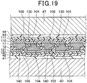
FIG. 19 is a view for explaining the method of manufacturing a heat flow measurement device. - Hereinafter, embodiments of the technique of the present disclosure will be described on the basis of the drawings. In the following embodiments, components that are identical or equivalent to each other are denoted by the same reference sign for the sake of explanation.
- The first embodiment of the present disclosure will be described with reference to the drawings. As illustrated in
FIGS. 1 and 2 , athermoelectric conversion device 10 according to the present embodiment integrally includes afirst insulator 11, asecond insulator 12, a frontsurface protection member 110, and a rearsurface protection member 120. Thethermoelectric conversion device 10 includes a plurality ofinterlayer connection members interlayer connection members surface wiring patterns 111 and rearsurface wiring patterns 121. Theinterlayer connection members - In
FIG. 2 , the frontsurface protection member 110 is regarded as transparent or translucent, and the positions of the plurality of frontsurface wiring patterns 111 are indicated by solid lines. InFIG. 2 , for the convenience of explanation, theinterlayer connection members - First, a method of manufacturing the
thermoelectric conversion device 10 will be described. - As illustrated in
FIGS. 1 and 2 , thefirst insulator 11 includes a flexible resin film and has a plate-like shape. Thefirst insulator 11 is configured as follows using the method of manufacturing thethermoelectric conversion device 10 described later. Specifically, thefirst insulator 11 includes a thermoplastic resin with a melting point higher than the temperature for solid-phase sintering first and secondconductive pastes 131 and 141 (refer toFIG. 15 , etc.) or a thermosetting resin. The resin contained in thefirst insulator 11 can be, for example, an aramid resin with an adhesive layer. - The
first insulator 11 has a plurality of first and second viaholes holes 101 and the second viaholes 102 are alternately provided in the surface direction of thefirst insulator 11. - The
second insulator 12 includes a flexible resin film and has a plate-like shape in the same manner as thefirst insulator 11. Thesecond insulator 12 is stacked on thefirst insulator 11 in its thickness direction. Thesecond insulator 12 includes a thermoplastic resin with a melting point higher than the temperature for solid-phase sintering of the first and secondconductive pastes 131 and 141 (described later) or a thermosetting resin. The resin contained in thesecond insulator 12 can be, for example, an aramid resin with an adhesive layer. - The
second insulator 12 has a plurality of third and fourth viaholes holes 103 and the fourth viaholes 104 are alternately provided in the surface direction of thesecond insulator 12. The third viaholes 103 of thesecond insulator 12 are provided at positions corresponding to the second viaholes 102 of thefirst insulator 11. The fourth viaholes 104 of thesecond insulator 12 are provided at positions corresponding to the first viaholes 101 of thefirst insulator 11. - The internal width of the fourth via
holes 104 of thesecond insulator 12 is larger than the internal width of the first viaholes 101 of thefirst insulator 11. The internal width of the second viaholes 102 of thefirst insulator 11 is larger than the internal width of the third viaholes 103 of thesecond insulator 12. Note that the internal width of the first viaholes 101 of thefirst insulator 11 is substantially equal to the internal width of the third viaholes 103 of thesecond insulator 12. The internal width of the second viaholes 102 of thefirst insulator 11 is substantially equal to the internal width of the fourth viaholes 104 of thesecond insulator 12. - A plurality of first
interlayer connection members 130 are embedded in the first viaholes 101 of thefirst insulator 11 and the fourth viaholes 104 of thesecond insulator 12. In addition, a plurality of secondinterlayer connection members 140 are embedded in the second viaholes 102 of thefirst insulator 11 and the third viaholes 103 of thesecond insulator 12. - The first
interlayer connection members 130 and the secondinterlayer connection members 140 include thermoelectric materials such as metals and semiconductors having different thermopowers so as to exhibit the Seebeck effect. For example, the firstinterlayer connection members 130 each include a metallic compound that contains solid-phase sintered p-type Bi-Sb-Te alloy powder so as to maintain the original crystal structure of a plurality of metallic atoms. For example, the secondinterlayer connection members 140 each include a metallic compound that contains solid-phase sintered n-type Bi-Te alloy powder so as to maintain the original crystal structure of a plurality of metallic atoms. - The surface of the
first insulator 11 that does not face thesecond insulator 12 is covered with the frontsurface protection member 110 provided with the frontsurface wiring patterns 111. In other words, the frontsurface protection member 110 covers the surface of thefirst insulator 11 that does not face thesecond insulator 12 and the frontsurface wiring patterns 111. The frontsurface protection member 110 includes a flexible resin film and has a plate-like shape in the same manner as thefirst insulator 11. The frontsurface protection member 110 includes a thermoplastic resin with a melting point higher than the temperature for solid-phase sintering of the first and secondconductive pastes 131 and 141 (described later) or a thermosetting resin. The resin contained in the frontsurface protection member 110 can be, for example, an aramid resin with an adhesive layer. - The front
surface wiring patterns 111 are patterned using copper foil or the like, and provided on the surface of the frontsurface protection member 110. The plurality of frontsurface wiring patterns 111 are electrically connected, in thefirst insulator 11, to the ends of the firstinterlayer connection members 130 that do not face thesecond insulator 12 and to the ends of the secondinterlayer connection members 140 adjacent thereto. - The surface of the
second insulator 12 that does not face thefirst insulator 11 is covered with the rearsurface protection member 120 provided with the rearsurface wiring patterns 121. In other words, the rearsurface protection member 120 covers the surface of thesecond insulator 12 that does not face thefirst insulator 11 and the rearsurface wiring patterns 121. The rearsurface protection member 120 includes a flexible resin film and has a plate-like shape in the same manner as thefirst insulator 11. The rearsurface protection member 120 includes a thermoplastic resin with a melting point higher than the temperature for solid-phase sintering of the first and secondconductive pastes 131 and 141 (described later) or a thermosetting resin. The resin contained in the rearsurface protection member 120 can be, for example, an aramid resin with an adhesive layer. - The rear
surface wiring patterns 121 are patterned using copper foil or the like, and provided on the surface of the rearsurface protection member 120. The plurality of rearsurface wiring patterns 121 are electrically connected, in thesecond insulator 12, to the other ends of the firstinterlayer connection members 130 that do not face thefirst insulator 11 and to the other ends of the secondinterlayer connection members 140 adjacent thereto. - The first and second
interlayer connection members surface wiring patterns interlayer connection members surface wiring patterns surface wiring patterns 111 or rearsurface wiring patterns 121 that connect the first and secondinterlayer connection members surface wiring patterns 111 or rearsurface wiring patterns 121 are exposed to outside air through metal members (not illustrated) or the like. The exposed parts serve as electrical connections between thethermoelectric conversion device 10 and an external detection device (not illustrated). - The heat flux that flows between one surface and the other surface of the
thermoelectric conversion device 10 in the thickness direction causes a difference in temperature between one end and the other end of each of the first and secondinterlayer connection members interlayer connection members thermoelectric conversion device 10 outputs the generated thermoelectric force as a sensor signal (e.g., voltage signal). - Next, a method of manufacturing the
thermoelectric conversion device 10 will be described. - As illustrated in
FIG. 3 , the manufacturing method according to the present embodiment includes a first insulator preparing step (S10), a second insulator preparing step (S20), a first conductive paste filling step (S30), and a second conductive paste filling step (S40). The manufacturing method according to the present embodiment also includes an insulator arranging step (S50), a front surface protection member preparing step (S60), a rear surface protection member preparing step (S70), a stacked body forming step (S80), and an integrating step (S90). - In the first insulator preparing step (S10), the above-mentioned
first insulator 11 is prepared. Then, drill working, laser working, or the like is performed on the preparedfirst insulator 11. Consequently, the first viaholes 101 and the second viaholes 102 are formed in the first insulator preparing step (S10). The first insulator preparing step (S10) in the present embodiment corresponds to a "first forming step". - In the second insulator preparing step (S20), the above-mentioned
second insulator 12 is prepared. Then, drill working, laser working, or the like is performed on the preparedsecond insulator 12. Consequently, the third viaholes 103 and the fourth viaholes 104 are formed in the second insulator preparing step (S20). The second insulator preparing step (S20) in the present embodiment corresponds to a "second forming step". - Note that, as described above, the internal width of the fourth via
holes 104 of thesecond insulator 12 is larger than the internal width of the first viaholes 101 of thefirst insulator 11. The internal width of the second viaholes 102 of thefirst insulator 11 is larger than the internal width of the third viaholes 103 of thesecond insulator 12. - Next, the first conductive paste filling step S30 of the method of manufacturing the
thermoelectric conversion device 10 will be described. - The first conductive paste filling step (S30) is the step of filling the first via
holes 101 of thefirst insulator 11 with the firstconductive paste 131. The first conductive paste filling step (S30) in the present embodiment corresponds to a "first filling step". As illustrated inFIG. 4 , the first conductive paste filling step (S30) includes a first mask providing step (S31), a first conductive paste supplying step (S32), a first conductive paste collecting step (S33), a first mask peeling step (S34), and the like. Note that, for example, the conductive material filling device described inJP 2010-50356 A - First, in the first mask providing step (S31), the following members are arranged on an adsorbing
metal plate 20 of a conductive material filling device (not illustrated) as illustrated inFIG. 6 . Specifically, in the first mask providing step (S31), adsorbingpaper 21, thefirst insulator 11, afirst mask 22, and afirst metal mask 23 are arranged on the adsorbingmetal plate 20 in this order. - A plurality of
holes 24 are provided in the adsorbingmetal plate 20. The space below the plurality ofholes 24 is connected to a vacuum pump (not illustrated). The adsorbingmetal plate 20 is heated by a heater (not illustrated). - The adsorbing
paper 21 arranged on the adsorbingmetal plate 20 can be any material that absorbs solvents used for theconductive pastes 131 and 141 (described later). For example, commonly available high-quality paper is used as the adsorbingpaper 21. Thefirst insulator 11 including the first and second viaholes paper 21. - The
first mask 22 is arranged on thefirst insulator 11. The thickness of thefirst mask 22 is larger than the thickness of thesecond insulator 12. Thefirst mask 22 has first mask holes 25 at positions corresponding to the first viaholes 101. The capacity of the first mask holes 25 is larger than the capacity of the fourth viaholes 104 of thesecond insulator 12. Note that the material for thefirst mask 22 can be, for example, an aramid resin. - The
first metal mask 23 is arranged on thefirst mask 22. Thefirst metal mask 23 may have any thickness as long as thefirst metal mask 23 is rigid enough to withstand the friction of a filling squeegee in the first conductive paste supplying step (S32) described later. Thefirst metal mask 23 has first metal mask holes 26 at positions corresponding to the first mask holes 25. Consequently, in the first mask providing step (S31), the adsorbingpaper 21, thefirst insulator 11, thefirst mask 22, and thefirst metal mask 23 are arranged on the adsorbingmetal plate 20 in this order. - Next, in the first conductive paste supplying step (S32), a filling
squeegee 27 is moved in the direction of arrow A on thefirst metal mask 23 as illustrated inFIGS. 6 and7 . Then, the firstconductive paste 131 is discharged from the fillingsqueegee 27. At this time, arear end 271 of the fillingsqueegee 27 relative to its moving direction is moved in contact with the upper surface of thefirst metal mask 23. Consequently, the firstconductive paste 131 is rubbed into the first viaholes 101 through the first metal mask holes 26 and the first mask holes 25 from above thefirst metal mask 23. Note that any excess firstconductive paste 131 is rubbed off using theend 271 of the fillingsqueegee 27. - The first
conductive paste 131 can be made, for example, by adding Bi-Sb-Te alloy fine powder whose metallic atoms maintain a certain crystal structure to an organic solvent such as paraffin so that a paste is obtained. - During the first conductive paste supplying step (S32), the
first insulator 11, thefirst mask 22, and thefirst metal mask 23 are heated by the above-mentioned heater to a temperature higher than the melting point of the organic solvent contained in the firstconductive paste 131. Consequently, in the first conductive paste supplying step (S32), the firstconductive paste 131 is supplied into the first metal mask holes 26, the first mask holes 25, and the first viaholes 101 with its organic solvent melted. - During the first conductive paste supplying step (S32), the first metal mask holes 26, the first mask holes 25, and the first via
holes 101 are evacuated by the above-mentioned vacuum pump. Consequently, in the first conductive paste supplying step (S32), no voids are included in the firstconductive paste 131 within the first metal mask holes 26, the first mask holes 25, and the first viaholes 101. - In the first conductive paste supplying step (S32), most of the organic solvent contained in the first
conductive paste 131 supply into the first metal mask holes 26, the first mask holes 25, and the first viaholes 101 is adsorbed by the adsorbingpaper 21. Therefore, in the first conductive paste supplying step (S32), the firstconductive paste 131 is supplied into the first metal mask holes 26, the first mask holes 25, and the first viaholes 101 from above thefirst metal mask 23, with its alloy fine powder densely packed. - Next, in the first conductive paste collecting step (S33), the
first metal mask 23 is removed from the upper surface of thefirst mask 22 as illustrated inFIGS. 8 and9 . Consequently, the firstconductive paste 131 within the first metal mask holes 26 protrudes from the upper surface of thefirst mask 22. Subsequently, in the first conductive paste collecting step (S33), ametal squeegee 28 is moved in the direction of arrow B on thefirst mask 22. Then, the firstconductive paste 131 protruding from thefirst mask 22 is scraped off. - Next, in the first mask peeling step (S34), the
first mask 22 is removed from thefirst insulator 11 as illustrated inFIGS. 10 and11 . Consequently, the firstconductive paste 131 within the first viaholes 101 of thefirst insulator 11 protrudes from the first viaholes 101 by the thickness of thefirst mask 22. As described above, the thickness of thefirst mask 22 is larger than the thickness of thesecond insulator 12. Therefore, the firstconductive paste 131 protrudes from the first viaholes 101 by an amount larger than the thickness of thesecond insulator 12. As described above, the capacity of the first mask holes 25 of thefirst mask 22 is larger than the capacity of the fourth viaholes 104 of thesecond insulator 12. Therefore, the volume of the parts of the firstconductive paste 131 protruding from the first viaholes 101 is larger than the capacity of the fourth viaholes 104 of thesecond insulator 12. - Next, the second conductive paste filling step (S40) of the method of manufacturing the
thermoelectric conversion device 10 will be described. The second conductive paste filling step (S40) is the step of filling the second viaholes 102 of thesecond insulator 12 with the secondconductive paste 141. The second conductive paste filling step (S40) in the present embodiment corresponds to a "second filling step". As illustrated inFIG. 5 , the second conductive paste filling step (S40) includes a second mask providing step (S41), a second conductive paste supplying step (S42), a second conductive paste collecting step (S43), a second mask peeling step (S44), and the like. - First, in the second mask providing step S41, the following members are arranged on the adsorbing
metal plate 20 of the conductive material filling device as illustrated inFIG. 12 . Specifically, in the second mask providing step (S41), the adsorbingpaper 21, thesecond insulator 12, asecond mask 29, and asecond metal mask 30 are arranged on the adsorbingmetal plate 20 in this order. The thickness of thesecond mask 29 arranged on thesecond insulator 12 is larger than the thickness of thefirst insulator 11. Thesecond mask 29 has second mask holes 31 at positions corresponding to the third viaholes 103. The capacity of the second mask holes 31 is larger than the capacity of the second viaholes 102 of thefirst insulator 11. Note that the material for thesecond mask 29 can be, for example, an aramid resin. - The
second metal mask 30 arranged on thesecond mask 29 has second metal mask holes 32 at positions corresponding to the second mask holes 31. - Next, in the second conductive paste supplying step (S42), the above-mentioned heater and vacuum pump are driven, and the filling
squeegee 27 is moved in the direction of arrow C on thesecond metal mask 30 as illustrated inFIG. 12 . Then, the secondconductive paste 141 is discharged from the fillingsqueegee 27. The secondconductive paste 141 can be made, for example, by adding Bi-Te alloy fine powder whose metallic atoms maintain a certain crystal structure to an organic solvent such as paraffin so that a paste is obtained. In the second conductive paste supplying step (S42), most of the organic solvent contained in the secondconductive paste 141 supply into the second metal mask holes 32, the second mask holes 31, and the third viaholes 103 is adsorbed by the adsorbingpaper 21. Therefore, in the second conductive paste supplying step (S42), the secondconductive paste 141 is supplied into the second metal mask holes 32, the second mask holes 31, and the third viaholes 103 from above thesecond metal mask 30, with its alloy fine powder densely packed. - Next, in the second conductive paste collecting step (S43), the
second metal mask 30 is removed from the upper surface of thesecond mask 29 as illustrated inFIG. 13 . Consequently, the secondconductive paste 141 within the second metal mask holes 32 protrudes from the upper surface of thesecond mask 29. Subsequently, in the second conductive paste collecting step (S43), themetal squeegee 28 is moved in the direction of arrow D on thesecond mask 29. Then, the secondconductive paste 141 protruding from thesecond mask 29 is scraped off. - Next, in the second mask peeling step (S44), the
second mask 29 is removed from thesecond insulator 12 as illustrated inFIG. 14 . Consequently, the secondconductive paste 141 within the third viaholes 103 of thesecond insulator 12 protrudes from the third viaholes 103 by the thickness of thesecond mask 29. As described above, the thickness of thesecond mask 29 is larger than the thickness of thefirst insulator 11. Therefore, the secondconductive paste 141 protrudes from the third viaholes 103 by an amount larger than the thickness of thefirst insulator 11. As described above, the capacity of the second mask holes 31 of thesecond mask 29 is larger than the capacity of the second viaholes 102 of thefirst insulator 11. Therefore, the volume of the parts of the secondconductive paste 141 protruding from the third viaholes 103 is larger than the capacity of the second viaholes 102 of thefirst insulator 11. - Next, the insulator arranging step (S50) of the method of manufacturing the
thermoelectric conversion device 10 will be described. - In the insulator arranging step (S50), the
first insulator 11 is arranged such that the parts of the firstconductive paste 131 protruding from the first viaholes 101 face the fourth viaholes 104 of thesecond insulator 12 as illustrated inFIG. 15 . Similarly, thesecond insulator 12 is arranged such that the parts of the secondconductive paste 141 protruding from the third viaholes 103 face the second viaholes 102 of thefirst insulator 11. - Next, the front surface protection member preparing step (S60) will be described.
- In the front surface protection member preparing step (S60), the front
surface protection member 110 having the frontsurface wiring patterns 111 is prepared as illustrated inFIG. 15 . The frontsurface wiring patterns 111 are arranged in the above-mentioned insulator arranging step (S50) in the following manner. Specifically, the frontsurface wiring patterns 111 are arranged at positions where they are connectable to the ends of the firstconductive paste 131 of thefirst insulator 11 that do not face thesecond insulator 12 and connectable to the ends of the secondconductive paste 141 protruding from the third viaholes 103 of thesecond insulator 12. The method of manufacturing the frontsurface wiring patterns 111 and the frontsurface protection member 110 first includes forming copper foil or the like on at least the surface of the frontsurface protection member 110 that faces thefirst insulator 11. The method further includes patterning the copper foil appropriately. The frontsurface wiring patterns 111 are formed on the frontsurface protection member 110 with this method. - Next, the rear surface protection member preparing step (S70) will be described.
- In the rear surface protection member preparing step (S70), the rear
surface protection member 120 having the rearsurface wiring patterns 121 is prepared. The rearsurface wiring patterns 121 are arranged in the above-mentioned insulator arranging step (S50) in the following manner. Specifically, the rearsurface wiring patterns 121 are arranged at positions where they are connectable to the other ends of the firstconductive paste 131 protruding from the first viaholes 101 of thefirst insulator 11 and connectable to the other ends of the secondconductive paste 141 of thesecond insulator 12 that do not face thefirst insulator 11. The method of manufacturing the rearsurface wiring patterns 121 and the rearsurface protection member 120 first includes forming copper foil or the like on at least the surface of the rearsurface protection member 120 that faces thesecond insulator 12. The method further includes patterning the copper foil appropriately. The rearsurface wiring patterns 121 are formed on the rearsurface protection member 120 with this method. - Next, the stacked body forming step (S80) will be described.
- In the stacked body forming step (S80), the following members are arranged on a lower pressing
plate 40 of a pressing machine as illustrated inFIG. 16 . Specifically, in the stacked body forming step (S80), alower buffer 41,lower release paper 42, the rearsurface protection member 120, thesecond insulator 12, thefirst insulator 11, the frontsurface protection member 110,upper release paper 43, and anupper buffer 44 are arranged on the lower pressingplate 40 in this order. - Note that the
lower buffer 41 and theupper buffer 44 can be, for example, Teflon (registered trademark). Thelower release paper 42 and theupper release paper 43 can be, for example, resin sheets formed of an aramid resin or the like. - The parts of the first
conductive paste 131 protruding from the first viaholes 101 of thefirst insulator 11 are inserted into the fourth via holes 104. The parts of the secondconductive paste 141 protruding from the third viaholes 103 of thesecond insulator 12 are inserted into the second via holes 102. The frontsurface protection member 110 is arranged such that the frontsurface wiring patterns 111 face the surface of thefirst insulator 11 that does not face thesecond insulator 12. The rearsurface protection member 120 is arranged such that the rearsurface wiring patterns 121 face the surface of thesecond insulator 12 that does not face thefirst insulator 11. Consequently, a stacked body is formed. - Next, the integrating step (S90) will be described.
- In the integrating step (S90), the stacked body arranged between the lower pressing
plate 40 and an upperpressing plate 47 of the pressing machine illustrated inFIG. 16 is heated while being pressed in the stacking direction in a vacuum. The integrating step (S90) includes a degassing step, a press molding step, a cooling step, and the like as illustrated inFIG. 17 . InFIG. 17 , the pressure (press pressure) applied to the stacked body and the temperature for heating the stacked body in the integrating step (S90) are indicated by solid line P and broken line Q, respectively. - As illustrated in
FIG. 17 , in the integrating step (S90), first, the degassing step is performed during the period from time T0 to time T1 (for example, for 600 seconds). In the degassing step, evacuation is performed with the vacuum pump, and the stacked body is heated at a temperature (for example, 180 °C) at which the first and secondconductive pastes conductive pastes - Consequently, the fourth via
holes 104 of thesecond insulator 12 are fully filled with the firstconductive paste 131 as illustrated inFIG. 18 . Similarly, the second viaholes 102 of thefirst insulator 11 are fully filled with the secondconductive paste 141. Meanwhile, the residual solvent that remains unadsorbed by the adsorbingpaper 21 in the above-mentioned conductive paste filling steps (S30 and S40) is evaporated. Then, the vapor of the solvent is released from the firstconductive paste 131 and the secondconductive paste 141 by applying a vacuum. - As described above, the volume of the parts of the first
conductive paste 131 protruding from the first viaholes 101 of thefirst insulator 11 is larger than the capacity of the fourth viaholes 104 of thesecond insulator 12. Therefore, parts of the firstconductive paste 131 protrude from the surface of thesecond insulator 12 close to the rearsurface protection member 120 in the direction away from thefirst insulator 11. Similarly, the volume of the parts of the secondconductive paste 141 protruding from the third viaholes 103 of thesecond insulator 12 is larger than the capacity of the second viaholes 102 of thefirst insulator 11. Therefore, parts of the secondconductive paste 141 protrude from the surface of thefirst insulator 11 close to the frontsurface protection member 110 in the direction away from thesecond insulator 12. Consequently, the frontsurface wiring patterns 111 and the secondconductive paste 141 are brought into contact with each other, and gaps are provided between the frontsurface wiring patterns 111 and thefirst insulator 11. Similarly, the rearsurface wiring patterns 121 and the first conductive past 131 are brought into contact with each other, and gaps are provided between the rearsurface wiring patterns 121 and thesecond insulator 12. - As illustrated in
FIG. 17 , in the integrating step (S90), the press molding step is performed during the period from time T1 to time T2 (for example, for 600 seconds). In the press molding step, evacuation is performed with the vacuum pump, and the stacked body is heated and pressed at a certain temperature (for example, 320 °C) and a certain pressure (for example, 10 MPa). The temperature for this step is such that the first and secondconductive pastes first insulator 11, thesecond insulator 12, the frontsurface protection member 110, and the rearsurface protection member 120 bond with each other. - As illustrated in
FIG. 19 , in the integrating step (S90), a load is applied from the lower pressingplate 40 to the rearsurface protection member 120 through thelower release paper 42 and thelower buffer 41. A load is also applied from the upper pressingplate 47 to the frontsurface protection member 110 through theupper release paper 43 and theupper buffer 44. Consequently, the frontsurface protection member 110 and the frontsurface wiring patterns 111 are deformed toward thefirst insulator 11 at positions where no firstconductive paste 131 is provided. Similarly, the rearsurface protection member 120 and the rearsurface wiring patterns 121 are deformed toward thesecond insulator 12 at positions where no secondconductive paste 141 is provided. Therefore, in the lower andupper buffers conductive pastes conductive pastes - As a result, in the integrating step (S90), loads are efficiently applied from the lower pressing
plate 40 to the first and secondconductive pastes lower buffer 41, thelower release paper 42, the rearsurface protection member 120, and the rearsurface wiring patterns 121. Simultaneously, loads are efficiently applied from the upper pressingplate 47 to the first and secondconductive pastes upper buffer 44, theupper release paper 43, the frontsurface protection member 110, and the frontsurface wiring patterns 111. Therefore, the first and secondconductive pastes interlayer connection members interlayer connection members surface wiring patterns first insulator 11, thesecond insulator 12, the frontsurface protection member 110, and the rearsurface protection member 120 are bonded together under pressure. - As illustrated in
FIG. 17 , in the integrating step (S90), the cooling step is performed during the period from time T2 to time T3 (for example, for 600 seconds). The cooling step includes continuing pressing the stacked body at a certain pressure (for example, 10 MPa) while lowering the temperature. Consequently, each member that constitutes thethermoelectric conversion device 10 is cooled, and thethermoelectric conversion device 10 is molded. After that, the lower pressingplate 40 and the upper pressingplate 47 are separated from thethermoelectric conversion device 10, and thethermoelectric conversion device 10 is taken out from the pressing machine. Thethermoelectric conversion device 10 manufactured in this manner includes thefirst insulator 11, thesecond insulator 12, the frontsurface protection member 110, and the rearsurface protection member 120, each containing a thermoplastic resin with a high melting point or a thermosetting resin. Thus, thethermoelectric conversion device 10 has a high heat resistance. - The present embodiment achieves the following effects.
- (1) With the method of manufacturing the
thermoelectric conversion device 10 according to the present embodiment, in the state where thefirst insulator 11, thesecond insulator 12, and the like are stacked, the firstconductive paste 131 protrudes from thesecond insulator 12 toward the rearsurface protection member 120. Similarly, the secondconductive paste 141 protrudes from thefirst insulator 11 toward the frontsurface protection member 110. In this state, the stacked body is heated while being pressed in the stacking direction, and loads are efficiently applied from the front and rearsurface wiring patterns conductive pastes conductive pastes interlayer connection members thermoelectric conversion device 10, each of the first andsecond insulators thermoelectric conversion device 10 with high heat resistance can be manufactured.
Thethermoelectric conversion device 10 manufactured with the manufacturing method according to the present embodiment further includes the following characteristics. - (2) The
thermoelectric conversion device 10 according to the present embodiment includes the first andsecond insulators conductive pastes second insulators second insulators thermoelectric conversion device 10 can be accurately set.
For example, suppose the thickness of thethermoelectric conversion device 10 is set to a large value so that the size of the first and secondinterlayer connection members thermoelectric conversion device 10 relative to heat flux can be increased.
Alternatively, for example, suppose the thickness of thethermoelectric conversion device 10 is set to a small value. In this case, the influence of airflow around a measurement target on the measurement of heat flow can be reduced. - (3) The
thermoelectric conversion device 10 according to the present embodiment includes the first andsecond insulators second insulators thermoelectric conversion device 10 can be formed in accordance with the shape of a measurement target by performing hot press working one or more times after manufacturing thethermoelectric conversion device 10. - (4) The
thermoelectric conversion device 10 according to the present embodiment includes the first andsecond insulators holes 101 to 104 are formed using drill working or the like, the first andsecond insulators thermoelectric conversion device 10 can be narrowed, and the number of first and secondinterlayer connection members thermoelectric conversion device 10 relative to heat flux can be increased. - (5) The
thermoelectric conversion device 10 according to the present embodiment includes thefirst insulator 11, thesecond insulator 12, the frontsurface protection member 110, and the rearsurface protection member 120, each containing the same type of resin (e.g., aramid resin or the like). Therefore, these resins are firmly bonded together in the integrating step (S90) of the method of manufacturing thethermoelectric conversion device 10.
Consequently, peeling of resins from thethermoelectric conversion device 10 due to bending or the like can be prevented. - (6) In the
thermoelectric conversion device 10 according to the present embodiment, the internal width of the fourth viaholes 104 of thesecond insulator 12 is larger than the internal width of the first viaholes 101 of thefirst insulator 11. Similarly, the internal width of the second viaholes 102 of thefirst insulator 11 is larger than the internal width of the third viaholes 103 of thesecond insulator 12.
Consequently, in the stacked body forming step (S80) of the method of manufacturing thethermoelectric conversion device 10, the parts of the firstconductive paste 131 protruding from the first viaholes 101 of thefirst insulator 11 can be easily inserted into the fourth via holes 104. Similarly, the parts of the secondconductive paste 141 protruding from the third viaholes 103 can be easily inserted into the second via holes 102.
As a result, this step can be performed in a short period of time. - (7) In the
thermoelectric conversion device 10 according to the present embodiment, the volume of the parts of the firstconductive paste 131 protruding from the first viaholes 101 of thefirst insulator 11 is larger than the capacity of the fourth viaholes 104 of thesecond insulator 12. Similarly, the volume of the parts of the secondconductive paste 141 protruding from the third viaholes 103 of thesecond insulator 12 is larger than the capacity of the second viaholes 102 of thefirst insulator 11.
Accordingly, in the integrating step (S90) of the method of manufacturing thethermoelectric conversion device 10, the fourth viaholes 104 are fully filled with the firstconductive paste 131 subjected to the loads from the front and rearsurface wiring patterns conductive paste 131 protrudes from the fourth viaholes 104 toward the rearsurface wiring patterns 121. Similarly, the second viaholes 102 are fully filled with the secondconductive paste 141 subjected to the loads from the front and rearsurface wiring patterns conductive paste 141 protrudes from the second viaholes 102 toward the frontsurface wiring patterns 111. Consequently, the first and secondconductive pastes surface wiring patterns interlayer connection members - (8) In the method of manufacturing the
thermoelectric conversion device 10 according to the present embodiment, the first conductive paste filling step (S30) includes the first mask providing step (S31), the first conductive paste supplying step (S32), the first conductive paste collecting step (S33), the first mask peeling step (S34), and the like. In the first mask providing step (S31), thefirst insulator 11 is covered with thefirst mask 22 having the first mask holes 25. Furthermore, the surface of thefirst mask 22 that does not face thefirst insulator 11 is covered with thefirst metal mask 23 having the first metal mask holes 26. In the first conductive paste supplying step (S32), the firstconductive paste 131 is supplied into the first metal mask holes 26, the first mask holes 25, and the first viaholes 101 from above thefirst metal mask 23. In the first conductive paste collecting step (S33), thefirst metal mask 23 is removed from the upper surface of thefirst mask 22. Then, the firstconductive paste 131 protruding from thefirst mask 22 is scraped off. In the first mask peeling step (S34), thefirst mask 22 is removed from thefirst insulator 11.
The second conductive paste filling step (S40) includes the second mask providing step (S41), the second conductive paste supplying step (S42), the second conductive paste collecting step (S43), the second mask peeling step (S44), and the like in the same manner as the first conductive paste filling step (S30).
Accordingly, thefirst mask 22 and thefirst metal mask 23 are used when the firstconductive paste 131 is supplied into the first viaholes 101 of thefirst insulator 11 with the method of manufacturing thethermoelectric conversion device 10. Consequently, the thickness of thefirst mask 22 can be reduced. Therefore, the amount of protrusion of the firstconductive paste 131 from the first viaholes 101 of thefirst insulator 11 can be reduced. Similarly, thesecond mask 29 and thesecond metal mask 30 are used when the secondconductive paste 141 is supplied into the third viaholes 103 of thesecond insulator 12 with the method of manufacturing thethermoelectric conversion device 10.
Consequently, the thickness of thesecond mask 29 can be reduced. Therefore, the amount of protrusion of the secondconductive paste 141 from the third viaholes 103 of thesecond insulator 12 can be reduced. Thus, the first andsecond insulators thermoelectric conversion device 10 can be reduced. - (9) With the method of manufacturing the
thermoelectric conversion device 10 according to the present embodiment, the first andsecond insulators conductive pastes - Consequently, the
thermoelectric conversion device 10 with high heat resistance can be manufactured. - The technique of the present disclosure is not limited to the above embodiment. The technique of the present disclosure may be appropriately changed within the range described in the scope of claims. The technique of the present disclosure covers various modifications and equivalent variations. The above embodiments are not unrelated to one another but can be appropriately combined unless it is clearly impossible to combine them. Components that constitute each of the above embodiments are not necessarily essential unless it is specified that the components are essential and unless it is considered that the components are clearly essential in principle. In the above embodiments, the number, value, amount, range, etc. of components of the embodiments are not limited to a specific number or range unless otherwise specified and unless these are clearly limited to a specific number or range in principle. In the above embodiments, the material, shape, positional relation, etc. of components and the like are not limited to the described material, shape, positional relation, etc. unless otherwise specified and unless these are clearly limited to a specific material, shape, positional relation, etc. in principle.
- For example, in the above embodiment, the thermoelectric conversion device includes the
first insulator 11, thesecond insulator 12, the frontsurface protection member 110 having the frontsurface wiring patterns 111, and the rearsurface protection member 120 having the rearsurface wiring patterns 121. However, the present disclosure is not limited to this embodiment. In another embodiment, insulating sheets may be additionally provided between thefirst insulator 11 and thesecond insulator 12, between thefirst insulator 11 and the frontsurface protection member 110, and between thesecond insulator 12 and the rearsurface protection member 120. - Alternatively, insulating sheets may be additionally provided on the surface of the front
surface protection member 110 that does not face thefirst insulator 11 and on the surface of the rearsurface protection member 120 that does not face thesecond insulator 12. - According to the first aspect disclosed in some or all of the above embodiments, a method of manufacturing a thermoelectric conversion device as an aspect of the technique of the present disclosure includes first, second, and third forming steps, first and second filling steps, an arranging step, first and second preparing steps, and a pressure bonding step.
- The first forming step includes forming first via holes and second via holes in a first insulator having a plate-like shape.
- The second forming step includes forming third via holes and fourth via holes in a second insulator having a plate-like shape.
- The first filling step includes filling the first via holes with a first conductive paste containing alloy powder and a solvent such that the first conductive paste protrudes from the first via holes by an amount larger than the thickness of the second insulator.
- The second filling step includes filling the third via holes with a second conductive paste containing alloy powder and a solvent different from those of the first conductive paste such that the second conductive paste protrudes from the third via holes by an amount larger than the thickness of the first insulator.
- The arranging step includes arranging the first insulator and the second insulator such that parts of the first conductive paste protruding from the first via holes of the first insulator face the fourth via holes of the second insulator and parts of the second conductive paste protruding from the third via holes of the second insulator face the second via holes of the first insulator.
- The first preparing step includes preparing a front surface protection member having front surface wiring patterns connectable to the ends of the first conductive paste of the first insulator that do not face the second insulator and connectable to the ends of the second conductive paste protruding from the third via holes of the second insulator.
- The second preparing step includes preparing a rear surface protection member having rear surface wiring patterns connectable to the other ends of the first conductive paste protruding from the first via holes of the first insulator and connectable to the other ends of the second conductive paste of the second insulator that do not face the first insulator.
- The third forming step includes inserting the parts of the first conductive paste protruding from the first via holes into the fourth via holes, and inserting the parts of the second conductive paste protruding from the third via holes into the second via holes. The third forming step further includes arranging the front surface protection member having the front surface wiring patterns on the first insulator such that the front surface protection member does not face the second insulator, and arranging the rear surface protection member having the rear surface wiring patterns on the second insulator such that the rear surface protection member does not face the first insulator, thereby forming a stacked body.
- The pressure bonding step includes forming first and second conductors by heating the stacked body while pressing the stacked body in the stacking direction and by solid-phase sintering of the first and the second conductive pastes. The pressure bonding step further includes electrically connecting the first conductor, the second conductor, the front surface wiring patterns, and the rear surface wiring patterns, and bonding the first insulator, the second insulator, the front surface protection member, and the rear surface protection member together under pressure.
- According to the second aspect, the internal width of the fourth via holes formed in the second insulator is larger than the internal width of the first via holes. Similarly, the internal width of the second via holes formed in the first insulator is larger than the internal width of the third via holes.
- Accordingly, when the first insulator and the second insulator are stacked, the parts of the first conductive paste protruding from the first via holes of the first insulator can be easily inserted into the fourth via holes. Similarly, the parts of the second conductive paste protruding from the third via holes can be easily inserted into the second via holes.
- According to the third aspect, the step of filling the first via holes with the first conductive paste (first filling step) includes making the volume of the parts of the first conductive paste protruding from the first via holes of the first insulator larger than the capacity of the fourth via holes of the second insulator after the stacked body is heated while being pressed in the stacking direction. Similarly, the step of filling the third via holes with the second conductive paste (second filling step) includes making the volume of the parts of the second conductive paste protruding from the third via holes of the second insulator larger than the capacity of the second via holes of the first insulator after the stacked body is heated while being pressed in the stacking direction.
- Accordingly, when the stacked body is heated while being pressed, the fourth via holes are fully filled with the first conductive paste subjected to the loads from the front and rear surface wiring patterns, and the first conductive paste protrudes from the fourth via holes toward the rear surface wiring patterns. Similarly, the second via holes are fully filled with the second conductive paste subjected to the loads from the front and rear surface wiring patterns, and the second conductive paste protrudes from the second via holes toward the front surface wiring patterns. Thus, the first and second conductive pastes are efficiently subjected to the loads from the front and rear surface wiring patterns and solid-phase sintered, and become the first and second conductors, respectively.
- According to the fourth aspect, the step of filling the first via holes with the first conductive paste (first filling step) includes a first mask providing step, a first conductive paste supplying step, a first conductive paste collecting step, a first mask peeling step, and the like. The first mask providing step includes covering the first insulator with a first mask having a thickness larger than the thickness of the second insulator and having first mask holes at positions corresponding to the first via holes. The first mask providing step further includes covering the surface of the first mask that does not face the first insulator with a first metal mask having first metal mask holes corresponding to the first mask holes of the first mask. The first conductive paste supplying step includes putting the first conductive paste into the first metal mask holes, the first mask holes, and the first via holes from above the first metal mask. The first conductive paste collecting step includes removing the first metal mask from the upper surface of the first mask. The first conductive paste collecting step further includes scraping off the first conductive paste protruding from the first mask. The first mask peeling step includes removing the first mask from the first insulator. The step of filling the third via holes with the second conductive paste (second filling step) includes a second mask providing step, a second conductive paste supplying step, a second conductive paste collecting step, and a second mask peeling step. The second mask providing step includes covering the second insulator with a second mask having a thickness larger than the thickness of the first insulator and having second mask holes at positions corresponding to the third via holes. The second mask providing step further includes covering the surface of the second mask that does not face the second insulator with a second metal mask having second metal mask holes corresponding to the second mask holes of the second mask. The second conductive paste supplying step includes putting the second conductive paste into the second metal mask holes, the second mask holes, and the third via holes from above the second metal mask. The second conductive paste collecting step includes removing the second metal mask from the upper surface of the second mask. The second conductive paste collecting step further includes scraping off the second conductive paste protruding from the second mask. The second mask peeling step includes removing the second mask from the second insulator.
- Accordingly, the first mask and the first metal mask are used when the first conductive paste is supplied into the first via holes of the first insulator with the method of manufacturing a thermoelectric conversion device. Consequently, the thickness of the first mask can be reduced. Therefore, the amount of protrusion of the first conductive paste from the first via holes of the first insulator can be reduced. Similarly, the second mask and the second metal mask are used when the second conductive paste is supplied into the third via holes of the second insulator with the method of manufacturing a thermoelectric conversion device. Consequently, the thickness of the second mask can be reduced. Therefore, the amount of protrusion of the second conductive paste from the third via holes of the second insulator can be reduced. Thus, the thickness of the first and second insulators can be reduced with this manufacturing method, and a thin thermoelectric conversion device can be manufactured.
- According to the fifth aspect, the first and second insulators each include a resin (thermoplastic resin) with a melting point higher than the temperature for solid-phase sintering of the first and second conductive pastes.
- Accordingly, a thermoelectric conversion device with high heat resistance can be manufactured.
- According to the sixth aspect, the first and second insulators each include a thermosetting resin.
- Accordingly, a thermoelectric conversion device with high heat resistance can be manufactured.
- According to the seventh aspect, a thermoelectric conversion device as an aspect of the technique of the present disclosure includes a first insulator, a second insulator, a plurality of first conductors, a plurality of second conductors, front surface wiring patterns, rear surface wiring patterns, a front surface protection member, and a rear surface protection member.
- The first insulator has a plate-like shape and has first and second via holes. The second insulator has a plate-like shape and has third via holes whose internal width is smaller than that of the second via holes and fourth via holes whose internal width is larger than that of the first via holes. The second insulator is stacked on the first insulator in its thickness direction. The plurality of first conductors are embedded in the first via holes of the first insulator and the fourth via holes of the second insulator and have a certain thermopower (first thermopower). The plurality of second conductors are embedded in the second via holes of the first insulator and the third via holes of the second insulator and have a thermopower (second thermopower) different from that of the first conductors.
The front surface wiring patterns are connected to, in the first insulator, the ends of the first conductors that do not face the second insulator and the ends of the second conductors. The rear surface wiring patterns are connected to, in the second insulator, the other ends of the first conductors that do not face the first insulator and the other ends of the second conductors.The front surface protection member covers the surface of the first insulator that does not face the second insulator and the front surface wiring patterns. The rear surface protection member covers the surface of the second insulator that does not face the first insulator and the rear surface wiring patterns. - A thermoelectric conversion device including this configuration can be manufactured using the above-mentioned manufacturing method. Thus, the thermoelectric conversion device with high heat resistance can be obtained.
-
- S10 ...
- First insulator preparing step (first forming step)
- S20 ...
- Second insulator preparing step (second forming step)
- S30 ...
- First conductive paste filling step (first filling step)
- S40 ...
- Second conductive paste filling step (second filling step)
- S50 ...
- Insulator arranging step (arranging step)
- S60 ...
- Front surface protection member preparing step (first preparing step)
- S70 ...
- Rear surface protection member preparing step (second preparing step)
- S80 ...
- Stacked body forming step (third forming step)
- S90 ...
- Integrating step
Claims (7)
- A method of manufacturing a thermoelectric conversion device comprising:a first forming step (S10) of preparing a first insulator (11) having a plate-like shape and forming first via holes (101) and second via holes (102) in the first insulator;a second forming step (S20) of preparing a second insulator (12) having a plate-like shape and forming third via holes (103) and fourth via holes (104) in the second insulator;a first filling step (S30) of filling the first via holes with a first conductive paste (131) containing alloy powder and a solvent such that the first conductive paste protrudes from the first via holes by an amount larger than a thickness of the second insulator;a second filling step (S40) of filling the third via holes with a second conductive paste (141) containing alloy powder and a solvent different from those of the first conductive paste such that the second conductive paste protrudes from the third via holes by an amount larger than a thickness of the first insulator;an arranging step (S50) of arranging the first insulator and the second insulator such that parts of the first conductive paste protruding from the first via holes of the first insulator face the fourth via holes of the second insulator and parts of the second conductive paste protruding from the third via holes of the second insulator face the second via holes of the first insulator;a first preparing step (S60) of preparing a front surface protection member (110) having front surface wiring patterns (111) connectable to ends of the first conductive paste of the first insulator that do not face the second insulator and connectable to ends of the second conductive paste protruding from the third via holes of the second insulator;a second preparing step (S70) of preparing a rear surface protection member (120) having rear surface wiring patterns (121) connectable to other ends of the first conductive paste protruding from the first via holes of the first insulator and connectable to other ends of the second conductive paste of the second insulator that do not face the first insulator;a third forming step (S80) of forming a stacked body by inserting the parts of the first conductive paste protruding from the first via holes into the fourth via holes, inserting the parts of the second conductive paste protruding from the third via holes into the second via holes, arranging the front surface protection member having the front surface wiring patterns on the first insulator such that the front surface protection member does not face the second insulator, and arranging the rear surface protection member having the rear surface wiring patterns on the second insulator such that the rear surface protection member does not face the first insulator; anda pressure bonding step (S90) of forming a first conductor and a second conductor by heating the stacked body while pressing the stacked body in a stacking direction and by solid-phase sintering of the first conductive paste and the second conductive paste, electrically connecting the first conductor, the second conductor, the front surface wiring patterns, and the rear surface wiring patterns, and bonding the first insulator, the second insulator, the front surface protection member, and the rear surface protection member together under pressure.
- The method of manufacturing a thermoelectric conversion device according to claim 1, wherein
an internal width of the fourth via holes formed in the second insulator is larger than an internal width of the first via holes, and
an internal width of the second via holes formed in the first insulator is larger than an internal width of the third via holes. - The method of manufacturing a thermoelectric conversion device according to claim 1 or 2, wherein
the first filling step includes making a volume of the parts of the first conductive paste protruding from the first via holes of the first insulator larger than a capacity of the fourth via holes after the stacked body is heated while being pressed in the stacking direction, and
the second filling step includes making a volume of the parts of the second conductive paste protruding from the third via holes of the second insulator larger than a capacity of the second via holes after the stacked body is heated while being pressed in the stacking direction. - The method of manufacturing a thermoelectric conversion device according to any one of claims 1 to 3, wherein
the first filling step includes:a first mask providing step (S31) of covering the first insulator with a first mask (22) having a thickness larger than a thickness of the second insulator and having first mask holes (25) at positions corresponding to the first via holes, and covering a surface of the first mask that does not face the first insulator with a first metal mask (23) having first metal mask holes (26) corresponding to the first mask holes of the first mask;a first conductive paste supplying step (S32) of putting the first conductive paste into the first metal mask holes, the first mask holes, and the first via holes from above the first metal mask;a first conductive paste collecting step (S33) of removing the first metal mask from the first mask and then scraping off the first conductive paste protruding from the first mask; anda first mask peeling step (S34) of removing the first mask from the first insulator, and the second filling step includes:a second mask providing step (S41) of covering the second insulator with a second mask (29) having a thickness larger than a thickness of the first insulator and having second mask holes (31) at positions corresponding to the third via holes, and covering a surface of the second mask that does not face the second insulator with a second metal mask (30) having second metal mask holes (32) corresponding to the second mask holes of the second mask;a second conductive paste supplying step (S42) of putting the second conductive paste into the second metal mask holes, the second mask holes, and the third via holes from above the second metal mask;a second conductive paste collecting step (S43) of removing the second metal mask from the second mask and then scraping off the second conductive paste protruding from the second mask; anda second mask peeling step (S44) of removing the second mask from the second insulator. - The method of manufacturing a thermoelectric conversion device according to any one of claims 1 to 4, wherein
the first insulator and the second insulator each include a resin with a melting point higher than a temperature for solid-phase sintering of the first conductive paste and the second conductive paste. - The method of manufacturing a thermoelectric conversion device according to any one of claims 1 to 4, wherein
the first insulator and the second insulator each include a thermosetting resin. - A thermoelectric conversion device comprising:a first insulator (11) having a plate-like shape and having first via holes (101) and second via holes (102);a second insulator (12) having a plate-like shape and having third via holes (103) whose internal width is smaller than that of the second via holes and fourth via holes (104) whose internal width is larger than that of the first via holes, the second insulator being stacked on the first insulator in its thickness direction;a plurality of first conductors (130) embedded in the first via holes of the first insulator and the fourth via holes of the second insulator and having a first thermopower;a plurality of second conductors (140) embedded in the second via holes of the first insulator and the third via holes of the second insulator and having a second thermopower different from that of the first conductors;front surface wiring patterns (111) connected, in the first insulator, to ends of the first conductors that do not face the second insulator and to ends of the second conductors;rear surface wiring patterns (121) connected, in the second insulator, to other ends of the first conductors that do not face the first insulator and to other ends of the second conductors;a front surface protection member (110) that covers a surface of the first insulator that does not face the second insulator and the front surface wiring patterns; anda rear surface protection member (120) that covers a surface of the second insulator that does not face the first insulator and the rear surface wiring patterns.
Applications Claiming Priority (2)
| Application Number | Priority Date | Filing Date | Title |
|---|---|---|---|
| JP2016106103A JP6447577B2 (en) | 2016-05-27 | 2016-05-27 | Thermoelectric conversion device and manufacturing method thereof |
| PCT/JP2017/019454 WO2017204275A1 (en) | 2016-05-27 | 2017-05-25 | Thermoelectric conversion device and manufacturing method for same |
Publications (2)
| Publication Number | Publication Date |
|---|---|
| EP3467889A1 true EP3467889A1 (en) | 2019-04-10 |
| EP3467889A4 EP3467889A4 (en) | 2019-05-01 |
Family
ID=60412298
Family Applications (1)
| Application Number | Title | Priority Date | Filing Date |
|---|---|---|---|
| EP17802861.9A Withdrawn EP3467889A4 (en) | 2016-05-27 | 2017-05-25 | THERMOELECTRIC CONVERSION DEVICE AND METHOD FOR MANUFACTURING THE SAME |
Country Status (7)
| Country | Link |
|---|---|
| US (1) | US10622535B2 (en) |
| EP (1) | EP3467889A4 (en) |
| JP (1) | JP6447577B2 (en) |
| KR (1) | KR20190002570A (en) |
| CN (1) | CN109196670B (en) |
| TW (1) | TWI642213B (en) |
| WO (1) | WO2017204275A1 (en) |
Families Citing this family (1)
| Publication number | Priority date | Publication date | Assignee | Title |
|---|---|---|---|---|
| WO2021200265A1 (en) * | 2020-03-30 | 2021-10-07 | リンテック株式会社 | Thermoelectric conversion module |
Family Cites Families (24)
| Publication number | Priority date | Publication date | Assignee | Title |
|---|---|---|---|---|
| JPH07162039A (en) * | 1993-12-10 | 1995-06-23 | Sharp Corp | Thermoelectric conversion device, heat exchange element, and device using them |
| JP3592395B2 (en) * | 1994-05-23 | 2004-11-24 | セイコーインスツル株式会社 | Thermoelectric conversion element and manufacturing method thereof |
| US6222243B1 (en) * | 1994-05-23 | 2001-04-24 | Seiko Instruments Inc. | Thermoelectric device |
| US5824561A (en) * | 1994-05-23 | 1998-10-20 | Seiko Instruments Inc. | Thermoelectric device and a method of manufacturing thereof |
| US6127619A (en) * | 1998-06-08 | 2000-10-03 | Ormet Corporation | Process for producing high performance thermoelectric modules |
| AU4551399A (en) * | 1998-06-08 | 1999-12-30 | Ormet Corporation | Process for production of high performance thermoelectric modules and low temperature sinterable thermoelectric compositions therefor |
| JP2001160632A (en) * | 1999-12-02 | 2001-06-12 | Yamaha Corp | Thermoelectric module |
| JP2003017723A (en) * | 2001-06-29 | 2003-01-17 | Shin Etsu Handotai Co Ltd | Method of manufacturing semiconductor thin film and method of manufacturing solar cell |
| JP3989486B2 (en) * | 2002-06-06 | 2007-10-10 | 古河電気工業株式会社 | Thermoelectric element module and manufacturing method thereof |
| JP4594601B2 (en) * | 2003-05-16 | 2010-12-08 | 日立電線株式会社 | Method for manufacturing crystalline silicon-based thin film solar cell and solar cell formed using the same |
| JP3828924B2 (en) * | 2004-01-19 | 2006-10-04 | 松下電器産業株式会社 | Thermoelectric conversion element, method for manufacturing the same, and thermoelectric conversion apparatus using the element |
| JP2005217353A (en) * | 2004-02-02 | 2005-08-11 | Yokohama Teikoki Kk | Thermoelectric semiconductor element, thermoelectric conversion module, and manufacturing method thereof |
| JP4901350B2 (en) * | 2005-08-02 | 2012-03-21 | 株式会社東芝 | Thermoelectric conversion device and manufacturing method thereof |
| CN100585896C (en) * | 2005-08-02 | 2010-01-27 | 株式会社东芝 | Thermoelectric device and method for manufacturing the same |
| JP2007095897A (en) * | 2005-09-28 | 2007-04-12 | Toshiba Corp | Semiconductor device and manufacturing method thereof |
| JP2010050356A (en) | 2008-08-22 | 2010-03-04 | Shin-Etsu Chemical Co Ltd | Process for manufacturing heterojunction solar cell and heterojunction solar cell |
| CN101807662B (en) * | 2009-02-18 | 2012-09-05 | 财团法人工业技术研究院 | Thermoelectric element and manufacturing method thereof, chip stacking structure and chip packaging structure |
| JP5664326B2 (en) * | 2011-02-22 | 2015-02-04 | 富士通株式会社 | Thermoelectric conversion module |
| JP5376087B1 (en) | 2012-05-30 | 2013-12-25 | 株式会社デンソー | Method for manufacturing thermoelectric conversion device |
| JP5939085B2 (en) * | 2012-08-23 | 2016-06-22 | 大日本印刷株式会社 | Temperature difference power generation unit |
| JP5831468B2 (en) * | 2013-01-24 | 2015-12-09 | 株式会社デンソー | Method for manufacturing thermoelectric conversion device |
| JP6032175B2 (en) * | 2013-10-25 | 2016-11-24 | 株式会社デンソー | Method for manufacturing thermoelectric conversion device |
| JP6183327B2 (en) * | 2014-09-30 | 2017-08-23 | 株式会社デンソー | Thermoelectric converter |
| JP2016072559A (en) * | 2014-10-01 | 2016-05-09 | トヨタ自動車株式会社 | Thermoelectric module with array of thermoelectric elements |
-
2016
- 2016-05-27 JP JP2016106103A patent/JP6447577B2/en not_active Expired - Fee Related
-
2017
- 2017-05-25 EP EP17802861.9A patent/EP3467889A4/en not_active Withdrawn
- 2017-05-25 US US16/304,707 patent/US10622535B2/en not_active Expired - Fee Related
- 2017-05-25 KR KR1020187034149A patent/KR20190002570A/en not_active Withdrawn
- 2017-05-25 WO PCT/JP2017/019454 patent/WO2017204275A1/en not_active Ceased
- 2017-05-25 CN CN201780032769.3A patent/CN109196670B/en active Active
- 2017-05-26 TW TW106117649A patent/TWI642213B/en not_active IP Right Cessation
Also Published As
| Publication number | Publication date |
|---|---|
| EP3467889A4 (en) | 2019-05-01 |
| TWI642213B (en) | 2018-11-21 |
| JP2017212389A (en) | 2017-11-30 |
| CN109196670A (en) | 2019-01-11 |
| WO2017204275A1 (en) | 2017-11-30 |
| TW201810739A (en) | 2018-03-16 |
| KR20190002570A (en) | 2019-01-08 |
| US20190252594A1 (en) | 2019-08-15 |
| CN109196670B (en) | 2022-11-22 |
| US10622535B2 (en) | 2020-04-14 |
| JP6447577B2 (en) | 2019-01-09 |
Similar Documents
| Publication | Publication Date | Title |
|---|---|---|
| JP5987444B2 (en) | Thermoelectric conversion device and manufacturing method thereof | |
| US6127619A (en) | Process for producing high performance thermoelectric modules | |
| US20080292874A1 (en) | Sintered power semiconductor substrate and method of producing the substrate | |
| US20190250049A1 (en) | Heat flux sensor module and method of manufacturing same | |
| JP4228677B2 (en) | Circuit board | |
| JP2014197660A5 (en) | ||
| CN101436556A (en) | Method for manufacturing semiconductor assembly | |
| CN105531818B (en) | The manufacturing method and semiconductor device of semiconductor device | |
| JPWO2017208950A1 (en) | Thermoelectric conversion substrate, thermoelectric conversion module, and method of manufacturing thermoelectric conversion substrate | |
| JP6721329B2 (en) | Power semiconductor device and manufacturing method thereof | |
| CN203216632U (en) | Electronic component | |
| JP5664475B2 (en) | Semiconductor device | |
| CN103517584A (en) | Manufacturing method of multilayer circuit board | |
| US20070226995A1 (en) | System and method for adhering large semiconductor applications to pcb | |
| US10622535B2 (en) | Thermoelectric conversion device and method of manufacturing the same | |
| CN102124560B (en) | Method for manufacturing electronic components | |
| CN105659398B (en) | The manufacturing method of thermoelectric conversion device | |
| JP2014063981A (en) | Wiring board and manufacturing method of the same | |
| JP6471241B2 (en) | Thermoelectric module | |
| US9768036B2 (en) | Power semiconductor substrates with metal contact layer and method of manufacture thereof | |
| JP6500841B2 (en) | Heat flow measuring device | |
| CN107667419B (en) | Method for manufacturing a circuit carrier | |
| WO2021220540A1 (en) | Temperature sensor array and mounting structure therefor | |
| CN107078204A (en) | The manufacture method of thermoelectric conversion device | |
| JP2006073943A (en) | Thermoelectric converter |
Legal Events
| Date | Code | Title | Description |
|---|---|---|---|
| STAA | Information on the status of an ep patent application or granted ep patent |
Free format text: STATUS: THE INTERNATIONAL PUBLICATION HAS BEEN MADE |
|
| PUAI | Public reference made under article 153(3) epc to a published international application that has entered the european phase |
Free format text: ORIGINAL CODE: 0009012 |
|
| STAA | Information on the status of an ep patent application or granted ep patent |
Free format text: STATUS: REQUEST FOR EXAMINATION WAS MADE |
|
| 17P | Request for examination filed |
Effective date: 20181203 |
|
| AK | Designated contracting states |
Kind code of ref document: A1 Designated state(s): AL AT BE BG CH CY CZ DE DK EE ES FI FR GB GR HR HU IE IS IT LI LT LU LV MC MK MT NL NO PL PT RO RS SE SI SK SM TR |
|
| AX | Request for extension of the european patent |
Extension state: BA ME |
|
| STAA | Information on the status of an ep patent application or granted ep patent |
Free format text: STATUS: EXAMINATION IS IN PROGRESS |
|
| A4 | Supplementary search report drawn up and despatched |
Effective date: 20190403 |
|
| RIC1 | Information provided on ipc code assigned before grant |
Ipc: H01L 35/32 20060101ALI20190328BHEP Ipc: H01L 35/34 20060101AFI20190328BHEP |
|
| 17Q | First examination report despatched |
Effective date: 20190430 |
|
| STAA | Information on the status of an ep patent application or granted ep patent |
Free format text: STATUS: THE APPLICATION HAS BEEN WITHDRAWN |
|
| 18W | Application withdrawn |
Effective date: 20190523 |