EP3465871B1 - Spannungsregelung in drahtlosen leistungsempfängern - Google Patents
Spannungsregelung in drahtlosen leistungsempfängern Download PDFInfo
- Publication number
- EP3465871B1 EP3465871B1 EP17728714.1A EP17728714A EP3465871B1 EP 3465871 B1 EP3465871 B1 EP 3465871B1 EP 17728714 A EP17728714 A EP 17728714A EP 3465871 B1 EP3465871 B1 EP 3465871B1
- Authority
- EP
- European Patent Office
- Prior art keywords
- receiver
- value
- rect
- capacitor
- voltage
- Prior art date
- Legal status (The legal status is an assumption and is not a legal conclusion. Google has not performed a legal analysis and makes no representation as to the accuracy of the status listed.)
- Active
Links
- 230000033228 biological regulation Effects 0.000 title description 10
- 239000003990 capacitor Substances 0.000 claims description 193
- 230000006870 function Effects 0.000 claims description 29
- 238000000034 method Methods 0.000 claims description 20
- 229910052454 barium strontium titanate Inorganic materials 0.000 claims description 15
- 230000004044 response Effects 0.000 claims description 12
- 230000001105 regulatory effect Effects 0.000 claims description 5
- 238000005259 measurement Methods 0.000 description 17
- 238000010586 diagram Methods 0.000 description 10
- 230000005540 biological transmission Effects 0.000 description 9
- 230000007423 decrease Effects 0.000 description 9
- 230000008859 change Effects 0.000 description 8
- 238000004891 communication Methods 0.000 description 8
- 238000001514 detection method Methods 0.000 description 7
- 230000001965 increasing effect Effects 0.000 description 6
- 238000012546 transfer Methods 0.000 description 5
- 230000008901 benefit Effects 0.000 description 4
- 230000001419 dependent effect Effects 0.000 description 4
- 230000003247 decreasing effect Effects 0.000 description 3
- 238000009499 grossing Methods 0.000 description 3
- 238000004519 manufacturing process Methods 0.000 description 3
- 230000001052 transient effect Effects 0.000 description 3
- 238000013459 approach Methods 0.000 description 2
- 230000000694 effects Effects 0.000 description 2
- 238000001914 filtration Methods 0.000 description 2
- 230000008569 process Effects 0.000 description 2
- 230000001276 controlling effect Effects 0.000 description 1
- 230000008878 coupling Effects 0.000 description 1
- 238000010168 coupling process Methods 0.000 description 1
- 238000005859 coupling reaction Methods 0.000 description 1
- 230000007613 environmental effect Effects 0.000 description 1
- 238000002847 impedance measurement Methods 0.000 description 1
- 230000001939 inductive effect Effects 0.000 description 1
- 230000007246 mechanism Effects 0.000 description 1
- 230000001404 mediated effect Effects 0.000 description 1
- 238000012544 monitoring process Methods 0.000 description 1
- 230000037361 pathway Effects 0.000 description 1
- 230000002093 peripheral effect Effects 0.000 description 1
- 238000013139 quantization Methods 0.000 description 1
- 230000035945 sensitivity Effects 0.000 description 1
- 230000003068 static effect Effects 0.000 description 1
- 230000001360 synchronised effect Effects 0.000 description 1
Images


Classifications
-
- H—ELECTRICITY
- H02—GENERATION; CONVERSION OR DISTRIBUTION OF ELECTRIC POWER
- H02J—CIRCUIT ARRANGEMENTS OR SYSTEMS FOR SUPPLYING OR DISTRIBUTING ELECTRIC POWER; SYSTEMS FOR STORING ELECTRIC ENERGY
- H02J50/00—Circuit arrangements or systems for wireless supply or distribution of electric power
- H02J50/10—Circuit arrangements or systems for wireless supply or distribution of electric power using inductive coupling
- H02J50/12—Circuit arrangements or systems for wireless supply or distribution of electric power using inductive coupling of the resonant type
-
- H—ELECTRICITY
- H01—ELECTRIC ELEMENTS
- H01F—MAGNETS; INDUCTANCES; TRANSFORMERS; SELECTION OF MATERIALS FOR THEIR MAGNETIC PROPERTIES
- H01F38/00—Adaptations of transformers or inductances for specific applications or functions
- H01F38/14—Inductive couplings
-
- H—ELECTRICITY
- H04—ELECTRIC COMMUNICATION TECHNIQUE
- H04B—TRANSMISSION
- H04B10/00—Transmission systems employing electromagnetic waves other than radio-waves, e.g. infrared, visible or ultraviolet light, or employing corpuscular radiation, e.g. quantum communication
- H04B10/60—Receivers
-
- H04B5/79—
Definitions
- the disclosure generally relates to wireless power systems and, more particularly, the disclosure relates to voltage regulation in wireless power receivers in wireless power systems.
- Wireless power receivers can receive power from wireless power transmitters via an oscillating magnetic field generated by the transmitter.
- Wireless power receivers can be coupled to electronic devices of varying power requirements.
- the power requirements of electronic devices, such as smartphones and laptops, can vary as the associated battery or batteries charge or discharge.
- WO 2015/119511 A1 relates to an inductive power receiver including a resonant circuit having a receiving coil and a tuning network, and a rectifier coupled to the resonant circuit and adapted to provide a DC output to a load.
- the tuning network is controlled to regulate the power provided to the load and includes a series tuning branch connected from the receiving coil to the rectifier, and a variable shunt tuning branch connected from a node between the series tuning branch and the receiving coil to a common ground on the DC output side of the rectifier.
- US 2015/244179 A1 relates to a receiver device in a coupled coil system for wireless energy transfer.
- the receiver device includes a receiver coil and a load device operatively connected to the receiver coil and configured to receive a signal from the receiver coil.
- An adjusting filter is included in the receiver device and is operatively connected between the receiver coil and the load device. The adjusting filter can be used to transform the effective resistance or impedance of the load as presented to the transformer during energy transfer so that the effective resistance or impedance of the load is maintained at a substantially constant level, and the signal received by the load device is maintained at a substantially constant level.
- the problem relates to improve the tuning of a wireless power receiver.
- a wireless power receiver includes a circuit comprising a tunable capacitor C 2 in parallel with an inductor L 1 , the wireless power receiver adapted to receive an induced voltage input V induced at the inductor L 1 due to a magnetic field generated by a wireless power transmitter, the wireless power receiver having an effective series resistance R receiver .
- the receiver further includes a rectifier coupled to the circuit, the rectifier having an output with a rectified voltage V rect and a rectified current I rect , and a controller having a first input for receiving a signal representative of the rectified voltage V rect and a first output for supplying an adjustment signal to the tunable capacitor C 2 .
- the controller can include a processor coupled to the first input and be configured to (i) operate on the signal representative of rectified voltage V rect to produce a desired capacitance value C 2 desired for capacitor C 2 and (ii) provide the adjustment signal determined so as to adjust a capacitance value C 2_value of capacitor C 2 to the desired capacitance value C 2_desired .
- the processor is configured to compare the signal representative of rectified voltage V rect to a range of voltages defined by an upper limit V upper and a lower limit V lower , the range of voltages stored in a memory of the controller; and the controller can be configured to transmit the adjustment signal to the tunable capacitor C 2 in response to the comparison of the value of rectified voltage V rect to the range of voltages.
- the controller to produce the desired capacitance value C 2_desired , is configured to (iii) receive, at a second input of the controller, a signal representative of a rectified current I rect of the rectifier output, (iv) operate, in the processor, on the signals representative of each of the rectified voltage V rect and current I rect to determine power P L to a load coupled to the rectifier output and resistance R L at the load, (v) operate, in the processor, on the receiver resistance R receiver and power P L to determine power P receiver to the receiver, and (vi) operate, in the processor, on power P receiver , to determine an open circuit voltage value V open , wherein the desired capacitance value C 2_desired is a function of V open .
- a wireless power receiver further includes a tunable capacitor C 3 coupled in series with the circuit, wherein the controller includes a second output for supplying an adjustment signal to the tunable capacitor C 3 .
- the memory of the controller includes a lookup table that includes capacitance values C 3_value for given capacitance values C 2 value and load voltage values V L_value , for at least one load resistance value R L_value .
- the controller selects the capacitance value C 3_value of the tunable capacitor C 3 such that the capacitance values C 2_value and C 3_value are resonant with the inductance L 1_value of inductor L 1 , with a resonance frequency f resonant .
- the resonant frequency f resonant is approximately 6.78 MHz.
- capacitor C 3 includes two or more capacitors coupled in parallel or in series.
- capacitor C 3 includes a switched capacitor, pulse width modulation (PWM) controlled capacitor, varactor, or barium strontium titanate (BST) capacitor.
- PWM pulse width modulation
- BST barium strontium titanate
- a wireless power receiver includes a means for adjusting a capacitance value C 3_value of capacitor C 3 .
- a wireless power receiver includes a means for adjusting a capacitance value C 2_value of capacitor C 2 .
- a wireless power receiver further includes a tunable capacitor C 3 coupled in series with the circuit, wherein the controller, during the operation, (v) transmits, via a second output coupled to the processor, an adjustment signal to the tunable capacitor C 3 to adjust a capacitance value C 3 value of the capacitor C 3 in response to the comparison of the value of rectified voltage V rect to the range of voltages.
- capacitor C 2 comprises two or more capacitors coupled in parallel or in series.
- a wireless power receiver further includes a tunable capacitor C 1 coupled in series with the inductor L 1 , wherein the controller includes a third output for supplying an adjustment signal to the tunable capacitor C 1 .
- a method for regulating rectified voltage V rect in a system including a controller coupled to a wireless power receiver, the wireless power receiver including a rectifier coupled to a circuit, the circuit comprising a tunable capacitor C 2 in parallel with an inductor L 1 , the wireless power receiver having an effective series resistance R receiver , the rectifier having an output with a rectified voltage V rect and a rectified current I rect .
- the method includes (i) receiving, at a first input of the controller, a signal representative of a rectified voltage V rect , (ii) operating, in a processor coupled to the first input, on the signal representative of the rectified voltage V rect to produce a desired capacitance value C 2_desired for capacitor C 2 , and (iii) providing, via a first output of the controller, an adjustment signal so as to adjust a capacitance value C 2_value of capacitor C 2 to the desired capacitance value C 2_desired .
- the method further includes (iv) comparing, by the processor, the signal representative of the rectified voltage V rect to a range of voltages defined by an upper limit V upper and lower limit V lower , the range of voltages stored in a memory of the controller, and (v) transmitting, via the first output of the controller, the adjustment signal to the tunable capacitor C 2 in response to the comparison of the signal representative of the value of rectified voltage V rect to the range of voltages.
- Producing the desired capacitance value C 2_desired further includes (iv) receiving, at a second input of the controller, a signal representative of a rectified current I rect , (v) operating, in the processor, on the signals representative of each of the rectified voltage V rect and current I rect to determine power P L to a load coupled to the rectifier output and resistance R L at the load, (vi) operating, in the processor, on the receiver resistance R receiver and power P L to determine power P receiver to the receiver, and (vii) operating, in the processor, on power P receiver to determine an open circuit voltage value V open , wherein the desired capacitance value C 2_desired is a function of V open .
- the method further includes (viii) transmitting, via a second output coupled to the processor, an adjustment signal to a tunable capacitor C 3 coupled in series with the circuit.
- the method further includes (ix) selecting, from a lookup table stored in a memory of the controller, a capacitance value C 3_value for given capacitance values C 2_value and load voltage values V L for at least one load resistance R L .
- the method further includes (x) adjusting, by the processor, the capacitance value C 3_value of the tunable capacitor C 3 such that the capacitance values C 2_value and C 3_value are resonant with the inductance L 1_value of inductor L 1 , with a resonance frequency f resonant .
- Voltage induced across receiver resonator coils can be loaded by receiver circuitry.
- the receiver resonator is coupled to an impedance matching network (IMN), a rectifier (passive or active), filtering, and a regulating converter producing a desired parameter (e.g. DC-DC voltage regulator presenting a fix voltage supply to a load).
- IFN impedance matching network
- a rectifier passive or active
- filtering and a regulating converter producing a desired parameter
- a desired parameter e.g. DC-DC voltage regulator presenting a fix voltage supply to a load.
- Battery chargers are a special example where power is typically regulated.
- a local control loop (either feedforward or feedback) can be used.
- additional regulation stages such as a DC-DC converter, can add power loss and complexity.
- a preferred alternative may be regulation via the IMN (utilizing tunable elements) and/or active rectifiers.
- Tuning elements can remove the need for additional costly or bulky regulation circuitry which can ultimately lower efficiency of power transmission to the load or battery of an electronic device.
- electronic devices include cell phones, laptops, tablets, fitness devices, watches, and the like.
- Tuning elements can also decrease sensitivity to manufacturing tolerances, environmental effects (such as temperature), and other varying parameters. Care must be taken that controlling the tuning element does not cause more loss, greater EMI issues, etc. that counteract the benefit of tuning.
- Using multiple, high Q (quality factor) tuning elements such as barium strontium titanate (BST) capacitors, can maintain high efficiency while performing regulation as well.
- BST barium strontium titanate
- Transient response Key metrics of voltage or power regulation in the receiver circuitry include transient response, steady-state error, transmitter drive efficiency, power dissipation in receiver (thermals, product requirement, safety), non-linear distortion (electromagnetic interference (EMI) - radiated and conducted).
- Transient responses which can be caused by load changes, changes in coupling, temperature drift, etc., necessitate some degree of compensation speed that may be implementation dependent. For example, the speed of control loops and communication between parts of the receiver and/or transmitter may limit the speed of response. Details of illustrative embodiments are discussed below.
- Fig. 1 shows a diagram of an exemplary embodiment of a wireless power transmission system including a wireless power transmitter 102 and wireless power receiver 104.
- the wireless power transmitter 102 includes a full-bridge differential RF inverter 106 coupled to a transmitter impedance matching network (IMN) 108 and a transmitter resonator coil 110.
- the wireless power receiver 104 includes a receiver resonator coil 112 coupled to a receiver IMN 114 and an RF rectifier 116.
- the receiver 104 may be coupled directly to a load such as a battery or battery manager of an electronic device. Note that the components of the transmitter IMN 108 and/or receiver IMN 114 may be tunable. Further, the inverter 106 and/or rectifier 116 may be tunable.
- switches (S T1 , S T2 , S T3 , S T4 ) of the inverter 106 and/or switches (S R1 , S R2 , S R3 , S R4 ) of the rectifier 116 may be controllable by controllers 118 and 120, respectively, to achieve variable dead-time, phase-shifting, etc.
- Fig. 2 shows a diagram of an exemplary embodiment of a wireless power transmission system including a wireless power transmitter 202 and wireless power receiver 204.
- the wireless power transmitter 202 includes a full bridge differential RF inverter 206 coupled to a transmitter impedance matching network (IMN) 208 and a transmitter resonator coil 210.
- the wireless power receiver 204 includes a receiver resonator coil 212 coupled to a receiver IMN 214 and an RF rectifier 216.
- the receiver 204 may be coupled directly to a load such as a battery or battery manager of an electronic device. Note that the components of the transmitter IMN 208 and receiver IMN 214 may be tunable.
- IMN 208 can include a tunable or fixed shunt cap 218 for a differential class E or F inverter.
- the inverter 206 and/or rectifier 216 may be tunable.
- the switches (S T1 , S T2 ) of the inverter 206 and/or switches (S R1 , S R2 , S R3 , S R4 ) of the rectifier 216 may be controllable by controller 218 and 220, respectively, to achieve variable dead-time, phase-shifting, etc.
- Fig. 3A shows an exemplary embodiment of a wireless power receiver including a receiver resonator coil 302 coupled to one or more capacitors and impedance matching components 304, one or more diodes 306, active clamp 308, inductors 309A and 309B, smoothing capacitor 310, load 312, one or more sensors 314, controller 316, and a wireless communication module 318.
- the wireless communication module 318 may be a wireless communication device (for example, Bluetooth Low Energy (BLE)) available on the electronic device 320 to which the receiver 322 is coupled.
- BLE Bluetooth Low Energy
- the active clamp 308 can be used as a circuit protection measure to ensure that voltage does not increase above a predetermined limit.
- the inductors 309A and 309B are used to filter out common-mode signals.
- the smoothing capacitor 310 can smooth ripple or variations in output rectifier voltage.
- the connection between the controller and the BLE can be mediated via serial peripheral interface ports 324, 326 on the receiver 322 and electronic device.
- the impedance matching components 304 may be variable capacitors, such as BST capacitors, PWM controlled capacitors, bank of capacitors, and the like.
- the one or more diodes used to rectify the oscillating energy captured at the receiver resonator coil may be Schottky diodes. It can be advantageous to use Schottky diodes due to their low forward voltage drop and fast switching. Note that Schottky diodes can be used on one leg (top) of the circuit while the other leg is a short.
- sensors can be used to sense current, voltage, and/or power along the current pathways within the receiver.
- An advantage to this system is that the voltage regulation is achieved at the IMN of the receiver, avoiding the use of a DC-DC converter.
- one or more of the components coupled to the receiver resonator coil can be co-packaged into an application-specific integrated circuit (ASIC) 328.
- ASIC application-specific integrated circuit
- an ASIC may include one or more impedance matching components 304, one or more diodes 306, active clamp 308, sensors 308, controller 316, and/or a wireless communication module.
- Fig. 3B shows an exemplary embodiment of a wireless power receiver including many of the components listed above for FIG. 3A .
- the receiver 330 includes a "split-coil" receiver resonator coil 332.
- the split coil is coupled to capacitor configuration 334 that is connected to ground. This configuration can mitigate common-mode (CM) signal issues. Note that the tuning of the top capacitor can be independent from the bottom capacitor.
- CM common-mode
- Fig. 4 shows an exemplary embodiment of a wireless power receiver including a receiver resonator coil 402 coupled to one or more capacitors and impedance matching components 404, a rectifying diode bridge 406, a controller/wireless communication module 408, inductors 409A and 409B, and a smoothing capacitor 410.
- the receiver 412 is coupled to a load 414 of an electronic device.
- the diode bridge 406 can be a full-bridge rectifier having Schottky diodes.
- the one or more components coupled to the receiver resonator coil 402 can be co-packaged into an ASIC 416.
- Fig. 5 shows an exemplary embodiment of a wireless power receiver including one or more receiver resonator coils 502, 504 coupled to one or more capacitors 506, 508 and a rectifier 510 with an output to a load.
- the receiver resonator coils 502, 504 can be switched in and out to be in parallel or series and result in a different overall inductance. For example, when switch A is closed (and switches B, C are open), the coils 502, 504 are coupled in series. When switches B and C are closed (and A is open), the coils 502, 504 are coupled in parallel. Further, each of the coils 502, 504 can be activated independently by closing either switch B or C.
- the capacitors 506, 508 can be tunable capacitors.
- the switches, capacitors, and rectifier can be packaged into an integrated circuit (such as an ASIC).
- the rectifier may be an active rectifier using switches.
- a wireless power receiver can include a receiver resonator coil coupled to a network of capacitors.
- the network capacitors can include one or more switch or PWM controlled capacitors. These switch controlled capacitors may be activated when the wireless power transmission system is operating at lower frequencies, such as 100 - 300 kHz.
- the capacitors can include one or more BST capacitors. The BST capacitors can be designed or chosen to have a quality factor Q cap equal to or greater than the quality factor of the resonator coil Q coil . These tunable capacitors may be activated when the wireless power transmission system is operating at higher frequencies, such as 1 MHz to 2.4 GHz (for example, 6.78 MHz or 13.56 MHz).
- the switched or tunable capacitor can be configured to operate at any ISM (Industrial, Scientific, or Medical) frequency band. This may allow the system to switch from one mode, for example, at 120 kHz, to another mode, at 6.78 MHz and have tuning capability at each of these modes.
- ISM International, Scientific, or Medical
- Fig. 6A shows an exemplary embodiment of a wireless power receiver 600 including a receiver resonator coil 602 coupled to a network of capacitors 604 and a rectifier 606 with an output to a load.
- the network of capacitors 604 can include any of the above described discrete or continuous tunable capacitors.
- a first subcircuit includes coil 602 coupled in series with capacitors C 1A , C 1B , C 1C , C 1D .
- a second subcircuit includes the first subcircuit coupled in parallel to capacitors C 2A , C 2B .
- a third subcircuit includes the second subcircuit coupled in series with capacitors C 3A , C 3B , C 3C , C 3D . This third subcircuit is coupled into a rectifier 606.
- capacitors C 1A and C 1B are connected in parallel to one another in the same position relative to coil 602.
- capacitor C 1A may be a discrete tunable capacitor while capacitor C 1B may be continuous tunable capacitor. This can provide both "coarse” and “fine” tuning for a capacitance at position C 1 .
- capacitor C 1A may be a type of capacitor that is suited for tuning at frequency or group of frequencies f 1 and capacitor C 1B may be a type of capacitor that is suited for tuning at frequency or group of frequencies f 2 .
- the wireless power receiver 600 may switch in capacitor C 1A (and may keep capacitor C 1B switched out). If the receiver 600 detects a transmitter capable of transmitting power at frequency f 2 , then the receiver 600 may switch in capacitor C 1B (and may keep capacitor C 1A switched out). Similar embodiments are relevant for each of the capacitors connected in parallel (Cic and C 1D , C 2A and C 2B , C 3A and C 3B , C 3C and C 3D ). Note that capacitors C 1A and C 1B are balanced with C 1C and C 1D . This can mitigate common mode signal issues. In some embodiments, one or more of these components along with the rectifier 608 may be packaged into an integrated circuit 610.
- the capacitors in network 604 can include one or more switch or PWM controlled capacitors, respectively. These switch controlled capacitors may be activated when the wireless power transmission system is operating at lower frequencies, such as 100 - 300 kHz.
- the capacitors in network 604 can include one or more BST capacitors, respectively.
- the BST capacitors can be designed or chosen to have a quality factor Q cap equal to or greater than the quality factor of the resonator coil Q coil .
- These tunable capacitors may be activated when the wireless power transmission system is operating at higher frequencies, such as 1 MHz - 2.4 GHz (for example, 6.78 MHz or 13.56 MHz).
- the switched or tunable capacitor can be configured to operate at any ISM (Industrial, Scientific, or Medical) frequency band. This may allow the system to switch from one mode, for example, at 120 kHz, to another mode, at 6.78 MHz and have tuning capability at each of these modes.
- Fig. 6B shows an exemplary embodiment of a wireless power receiver 608 including a "split" receiver resonator coil 602A, 602B coupled to a network of capacitors 612 and a rectifier 614 with an output voltage V rect to a load.
- a first subcircuit includes coil 602A, 602B coupled in series with capacitors C 1E , C 1F .
- a second subcircuit includes the first subcircuit coupled in parallel to capacitors C 2A , C 2B .
- a third subcircuit includes the second subcircuit coupled in series with capacitors C 3A , C 3B , C 3C , C 3D . This third subcircuit is coupled into a rectifier 606.
- capacitors C 1E and C 1F are connected in parallel to one another. As described above for capacitors C 1A and C 1B , C 1E and C 1F can be different types of capacitors or can be configured to be activated or switched in at different frequencies. In some embodiments, particular sets of capacitors may be switched in or out based on the detection of a protocol or standard of wireless power transmission that the transmitter utilizes.
- Fig. 7 shows an exemplary embodiment of a receiver 700 with a tunable impedance matching network.
- the receiver 700 includes a resonator coil 702 coupled in series to capacitor C 1 .
- a voltage sensor 704 that measures voltage V 1 .
- the differential voltage measurements V c1 , V c2 are fed into integrator INT.
- a peak detector PD is used to detect the amplitude P (as function of time) of the measured voltage signal V 1 .
- the voltage signal is also fed into a mixer (SIN and COS) and one or more filters (LPF) to detect the phase of the voltage signal V 1 .
- SIN and COS mixer
- LPF filters
- the amplitude and phase measurements can be used by a controller to tune system components, such as the tunable capacitors C 1 , C 2 , and C 3 , or control other parts of the receiver, such as rectification or safety mechanisms.
- capacitor C 2 coupled in parallel to the voltage sensor 704 is capacitor C 2 .
- a current sensor 706 can be positioned between voltage sensor 704 and capacitor C 2 to measure coil current I coil .
- Coupled in series to the C 2 is a capacitor C 3 .
- a current sensor 708 can be positioned between C 2 and C 3 to measure current I 3 .
- Each of these current sensors 706 and 708 can be connected to amplitude and phase measurement circuits as described above for voltage sensor 704.
- Coupled in series to capacitor C 3 is inductor L 3 ′ (balanced) and rectifier 710.
- the rectifier 710 can be an active rectifier, such as a synchronous rectifier.
- the rectified voltage output V rect may be fed directly to a load or though other circuitry, such as voltage clamps or filters (see FIGs. 3A , 3B , and 4 ).
- tunable capacitors C 1 , C 2 , and C 3 may be controlled by a controller 712. Note that the outputs of the various sensors 704, 706, and 708 can be fed into component 712.
- the controller 712 in addition to some or all of components INT, PD, SIN and COS, and LPF may be integrated into an integrated circuit 714, such as an ASIC.
- the input signal may be a signal representing a measured current or voltage at a location within a power transfer system.
- the input signal may be, for example, a voltage signal representing a measured current or voltage at a location within a power transfer system, and can be represented by A IN ⁇ sin( ⁇ t + ⁇ ), where ⁇ is the phase of the input signal relative to the reference signals.
- the input signal can be the output of a Rogowski coil positioned within the circuitry of a power transfer system to measure a current signal.
- the signal mixers are coupled with the signal supply (such as the voltage signal V 1 ) so as to receive one of the reference signals as one input and the input signal as another input.
- the mixers (SIN and COS) mix (e.g., perform time-domain multiplication) a respective reference signal with the input signal and output mixed signal 1 and 2.
- LPF Low-pass Filters
- the filters may remove the second order harmonics generated from the signal mixing process as well as any higher order harmonics that were present in either reference signals or the input signal.
- the controller receives the mixed signals Q and I, determines the phase of the input signal, and outputs the phase of the input signal to, for example, IMN control circuitry.
- Impedance at the operating frequency can be determined using a ratio of Q to I.
- the impedance can be input to detection algorithms such as rogue object detection, foreign object detection, RFID detection, proximity detection, coil alignment, and the like.
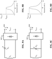
- Fig. 8A shows a receiver resonator coil L 1 coupled in series to a tunable capacitor C 1 .
- the foregoing circuit is coupled to a rectifier 802 with an output of a rectified voltage V rect,1 .
- Fig. 8B shows rectified voltage as a function of tuning C 1 for the circuit of Fig. 8A coupled to a load at the output 804 of the rectifier.
- the peak of the rectified voltage V rect,1 can be at most the voltage V peak,1 induced by the transmitter on the receiver resonator coil L 1 .
- This condition may be met when inductor L 1 is at resonance with capacitor C 1 , when impedance is at its lowest. For example, if V rect,1 is too high, C 1 may be tuned away or detuned from resonance with L 1 to decrease V rect,1 .
- Fig. 8C shows a receiver resonator coil L 1 coupled in parallel to capacitor C 2 .
- the foregoing circuit is coupled to a rectifier 802 with an output of a rectified voltage V rect,2 .
- Fig. 8D shows that rectified voltage V rect,2 is at its maximum V peak,2 when capacitor C 1 is at resonance with inductor L 1 for the circuit of Fig. 8C coupled to a load at the output 804 of the rectifier. Note that: V peak , 2 ⁇ V peak , 1 Thus, this circuit can be considered a "boost" to the voltage supplied by the transmitter.
- rectified voltage V rect,2 may be too large and an additional series element, such as capacitor C 1 , as shown in Fig. 8E , or capacitor C 3 , as shown in FIG. 8G , may be utilized.
- Fig. 8E shows a receiver resonator coil L 1 coupled in series with capacitor C 1 and in parallel with capacitor C 2 .
- the foregoing circuit is coupled to a rectifier 802 with an output of a rectified voltage V rect,3
- capacitors C 1 and C 2 can be used resonate with L 1 in different ratios. Similarly, these capacitors can be used to detune the resonator in different ratios.
- Inductance L 1 ′ is less than inductance L 1 leading to a lower rectified voltage.
- the peak V peak,3 of rectified voltage V rect,3 can be approximately described by the following: V peak , 2 ⁇ V peak , 3 ⁇ V peak , 1
- V rect,3 increases with an increase in C 1 .
- capacitance C 2 has a correlating decrease with an increase in C 1 .
- Fig. 8G shows a receiver resonator coil L 1 coupled in parallel to C 2 .
- Coil L 1 and C 2 are coupled in series to C 3 .
- the foregoing circuit is coupled to a rectifier 802 with an output of a rectified voltage V reet,4 .
- parallel capacitor C 2 can boost the rectified voltage.
- series capacitor C 3 can compensate for a varying load.
- Fig. 8H shows an equivalent circuit for Fig. 8G
- L 1 " is the parallel equivalent of inductance L 1 and capacitance C 2
- Inductance L 1 " is greater than inductance L 1 leading to a higher rectified voltage.
- capacitor C 3 in the receiver matching network can maximize the current to the load.
- the tuning of capacitor C 3 in the receiver matching network can increase or decrease the overall Thevenin output impedance of the receiver.
- a tunable capacitor C 3 can also be used to compensate for the detuning of inductor L 1 .
- the peak V peak,4 of rectified voltage V rect,4 can be approximately described by the following: V peak , 2 ⁇ V peak , 4 ⁇ V peak , 1 .
- the receiver-side capacitors are kept tuned to resonance to maximize efficiency. In some embodiments, if the receiver is detuned, the receiver-side capacitors may be retuned as a first step. If resonance cannot be achieved at the receiver, then the receiver may communicate with the transmitter to tune the transmitter-side capacitors.
- Fig. 9 shows an exemplary embodiment of a wireless power receiver 900 receiving wireless power from a power transmitter 902.
- the receiver includes a receiver resonator coil L 1 , impedance matching network (IMN) 904, rectifier 906, and controller 908.
- the controller 908 includes a processor 909.
- the controller 908 can be coupled to a processor 909.
- the receiver can be coupled to a load 910 in an electronic device such as the battery of a cell phone, laptop, tablet, and the like.
- the controller 908 can be coupled to sensors (such as current and voltage sensors) that provide measurements to a control loop.
- the controller 908 can tune elements of the IMN 904 to regulate the power to the load 910 and/or achieve high efficiency power transmission to the load 910.
- the controller 908 can be integrated within or coupled to a wireless communication module (such as a Bluetooth module).
- a voltage clamp can be included for start-up conditions (for example, with a large initial spike in voltage) and potential error conditions.
- the exemplary system utilizes a feedback loop to control components of the IMN 904 of the wireless power receiver 900 to optimize the power efficiency of the receiver.
- the components of the IMN 904 can be inductors and/or capacitors and the value of these components can be changed in a discrete or continuous fashion.
- One implementation of this approach is where the IMN is formed with variable capacitors, such as BST capacitors, PWM-controlled capacitors, or another implementation is where the IMN is formed with an array or bank of discrete capacitors using switches to change the value of the capacitance.
- Fig. 10A shows an exemplary embodiment of a control loop to tune the receiver IMN 904.
- the tunable IMN can be controlled by a control loop that includes feedback information from the wireless power transmitter 902 and information at the receiver load 910 to optimize the system efficiency.
- System efficiency can be defined as the ratio of power into the load at the receiver to input power at the transmitter, P load /P in .
- the control loop can change the components of the receiver IMN 904 such that the efficiency P load /P in is maximized.
- a voltage, current, or power sensor at the input power to the transmitter can measure or calculate input power.
- a voltage, current, or power sensor at the input to the load 910 can measure or calculate output power.
- a processor within a controller or coupled to the controller can calculate system efficiency using the above ratio. The controller can, in response, adjust the components C 2 and/or C 3 of the receiver IMN 904.
- a first step 1002 if other measurements are known (such as resistance of the transmitter coil) current I 1 in the transmitter resonator coil can be measured and an input power P in,Tx_coil can be calculated.
- the output voltage V out can be measured at the receiver load 910 and output power P load can be calculated using an additional current or resistance measurement.
- the processor can calculate the system efficiency by taking the ratio P load /P in,Tx_coil .
- the controller can, in response, adjust the components C 2 and/or C 3 of the receiver IMN 904. In some embodiments, the controller can adjust C 2 and measure the effect on the output voltage. If the outcome is not desired, the controller may return C 2 to its previous value and/or adjust C 3 and measure the effect on the output voltage until a desired outcome is achieved.
- Fig. 10B shows an exemplary embodiment of control loop to tune the receiver IMN 904.
- a receiver control loop can maximize power delivered to the load 910. This can be as part of the control loop in maximizing system efficiency or a local control loop at the receiver. If the power transmitted from the wireless power transmitter is approximately constant, then the receiver can have a local control loop to maximize P load . This can decrease complexity and computational effort.
- the feedback loop can be implemented in an analog, digital, or mixed-signal (analog and digital) circuits with or without a controller.
- voltage, current, or power can be measured or calculated at the input to the load 910.
- the efficiency of the receiver can be calculated assuming that a constant current at the transmitter.
- the efficiency of the receiver can be calculated by taking a voltage, current, and/or power measurement at the receiver resonator coil and calculating an input power P in,Rx_coil and comparing to P load .
- the controller can, in response, adjust the components C 2 and/or C 3 of the receiver IMN 904.
- Fig. 10C shows an exemplary embodiment of control loop to tune the receiver IMN 904.
- a receiver control loop can tune the IMN 904 to hit a target voltage V target for the load 910.
- a target voltage V target could be a voltage at or near the maximum input voltage V max of the load 910.
- V max of the load such as a battery charger input
- the wireless power receiver efficiency is optimized.
- the use of a DC-to-DC converter can be avoided and thus, the efficiency of the wireless power receiver can be further optimized. In other words, the losses that may be attributable to a DC-to-DC converter may be avoided.
- An advantage of tuning the receiver IMN 904 based on the load voltage is that the rectifier output can be ensured to be in a safe operating region.
- the safe operating region can be ensured because the feedback loop is adjusting the IMN 904 components such that the rectifier output achieves the target load voltage V target .
- the load of the wireless power receiver is a battery charging integrated circuit with a maximum input voltage of 20V.
- the target load voltage V target ideally can be 20V but will likely be set to a lower voltage, for example 19V, due to ripple and other non-idealities coming from the rectifier.
- the controller 908 on the wireless power receiver can be a negative feedback loop that regulates the rectifier output voltage to the target load voltage. The loop would compare the rectifier output voltage and compare it to the target voltage, in this example 19V, to generate an error signal. This error signal would then change the components of the IMN 904 (for example, capacitors C 2 and C 3 ) such that the rectifier output voltage is equal to the target voltage, resulting in no error signal.
- Implementation of the feedback loop can be implemented in the analog domain using operational amplifiers and PWM signals with variable capacitors and/or in the mixed signal analog and digital domain using analog-to-digital converters, comparators, microcontrollers, digital logic, firmware, switches and capacitor banks.
- a combination of continuously variable capacitors for fine tuning while switches and capacitor banks can be used for coarse tuning.
- the wireless power receiver can be embedded into a pre-defined system, for example a laptop, cell phone, etc.
- the target voltage can be known a priori and can be easily inputted or programmed into the controller or memory unit.
- the target voltage does not need to be static and can be changed, for example, by a user of the system or different safety conditions.
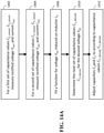
- Fig. 11 shows an exemplary embodiment of a control scheme for the regulation of rectified voltage of a wireless power receiver.
- Inputs to this control scheme can come from measurements (i.e. from sensors) of rectified voltage V rect , currents I 1 , I 2 , I 3 (see FIG. 7 ), and/or voltages in the matching network.
- V rect rectified voltage
- currents I 1 , I 2 , I 3 currents I 1 , I 2 , I 3 (see FIG. 7 ), and/or voltages in the matching network.
- rectified voltage is measured and, at step 1104, compared to a target voltage V target , within some error, hysteresis, or approximation interval ⁇ .
- target values of rectified voltage can be 1V, 5V, 10V, and 20V in consumer electronics such as mobile electronics and laptops.
- this interval ⁇ can be 1%, 5%, 10%, or more of target voltage V target .
- this interval can be 10 - 100 mV in a 10V system. If the voltage measurement is a digital signal, comparison of V rect to V target can depend on number of bits or quantization, at or above noise floor.
- V rect is less than V target - ⁇
- reactance X 2 of capacitor C 2 is compared to a minimum reactance value X 2,min . If X 2 is less than or equal to X 2,min , at step 1108, transmitter current I TX can be increased.
- the receiver can signal the transmitter to increase I TX .
- the transmitter can detect the measurements at the receiver and adjust current I TX accordingly. This may be accomplished by sending a control signal from the receiver to the transmitter. In some embodiments, the transmitter may be monitoring the receiver and may sense this condition. Once current I TX is increased, V rect can be measured at step 1102.
- X 2 is greater than X 2,min , at step 1110, X 2 can be decreased, for example, by tuning capacitor C 2 .
- V rect is monitored and at step 1114, reactance X 3 of capacitor C 3 is increased. For example, if tuning of C 3 is discrete (i.e. via a bank of capacitors) and increasing X 3 causes V rect to be out of the hysteresis band ⁇ , steps 1110 to 1114 may be cycled through to stabilize V rect . Control passes back to step 1102.
- step 1104 if V rect equals V target within ⁇ and reactance X 2 does not equal maximum reactance X 2,max , then control passes back to step 1102.
- step 1104 if V rect is greater than V target + ⁇ , then X 2 is compared to maximum reactance X 2,max at step 1116. If X 2 is less than X 2,max , at step 1118, X 2 is increased. Control passes back to step 1116. If X 2 is greater or equal to X 2,max , at step 1120, reactance X 3 is compared to X 3,min . If X 3 is greater than X 3,min , at step 1122, X 3 is decreased and control passes back to V rect . If X 3 is less than or equal to X 3,min , at step 1124, transmitter current I TX can be decreased. In some embodiments, the receiver can signal the transmitter to increase I TX . In some embodiments, the transmitter can detect the measurements at the receiver and adjust current I TX accordingly.
- Tuning loop #4 Regulate rectified voltage V rect
- the rectified voltage may be regulated by adjusting the capacitance value of the one or more capacitors in position C 2 (see at least Figs. 8C , 8E, or 8G ).
- the adjustment value may depend on the maximum dissipation power allowed in the receiver resonator, of which capacitor C 2 is a part.
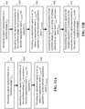
- Fig. 12A is a flowchart of an exemplary method for a wireless power receiver having a controller. Note that each of the following steps can be executed by the controller coupled to components of the receiver. Examples of such controllers are shown in at least Figs. 1-4 , 7 , and 9 .
- Step 1202 receives, at a first input of the controller, a value signal representative of a rectified voltage V rect .
- Step 1204 operates, in a processor coupled to the first input, on the signal representative of the rectified voltage V rect to produce a desired capacitance value C 2 desired for capacitor C 2 .
- Step 1206 provides, via a first output of the controller, an adjustment signal so as to adjust a capacitance value C 2_value of capacitor C 2 to the desired capacitance value C 2_desired .
- Fig. 12B is a flowchart of an exemplary method for a wireless power receiver having a controller that includes steps 1202-1206.
- the exemplary method also includes step 1208 which compares, by the processor, the signal representative of the rectified voltage V rect to a range of voltages defined by an upper limit V upper and lower limit V lower , the range of voltages stored in a memory of the controller.
- Step 1210 transmits, via the first output of the controller, the adjustment signal to the tunable capacitor C 2 in response to the comparison of the signal representative of the value of rectified voltage V rect to the range of voltages.
- Fig. 12C is a flowchart of an exemplary method for producing the desired capacitance value C 2_desired of step 1204 in Figs. 12A-12B .
- Step 1212 receives at a second input of the controller, a signal representative of a rectified current I rect .
- I rect can be sensed, measured, or calculated at the output of the rectifier of the receiver.
- Step 1214 operates, in the processor, on the signals representative of each of the rectified voltage V rect and current I rect to determine power P L to a load coupled to the rectifier output and resistance R L at the load.
- the power P L and resistance R L can be calculated from these measurements:
- Step 1216 operates, in the processor, on the receiver resistance R receiver and power P L to determine power P receiver to the receiver.
- Step 1218 operates, in the processor, on power P receiver , a value of capacitor C 2 , and a value of capacitor C 3 to determine an open circuit voltage value V open , wherein the desired capacitance value C 2_desired is a function of V open .
- the values of capacitors C 2 and C 3 can be a most recent measurement or estimation.
- Z th Z 3 + Z 1 Z 2 Z 1 + Z 2
- Z 1 R 1 + j ⁇ L 1
- Z 2 R 2 + 1 j ⁇ C 2
- Z 3 R 3 + 1 j ⁇ C 3 .
- V AC V L Z th R L .
- C 2_ desired 2 ⁇ 2 L d ⁇ 4 ⁇ 4 L d 2 ⁇ 4 ⁇ 4 L d 2 + ⁇ 2 R d 2 1 ⁇ Vac Vopen 2 2 ⁇ 4 L d 2 + ⁇ 2 R d 2 .
- V ocmax is the maximum open circuit voltage value that is dependent on the circuit. It can be helpful to determine the maximum capacitance value C 2_max such that the value of capacitor C 2 has an upper limit. This may mitigate any potential harm or damage from high voltages in the receiver.
- the value of C 2_desired can equal the value C 2_max .
- a desirable value for capacitor C 3 can be determined with the goal of obtaining a rectified voltage V rect within a range of V upper and V lower .
- the capacitance value of C 3 can be determined by a lookup table that stores the values of C 2 , C 3 pairs.
- the approximate relationship between C 2 and C 3 is that, for a higher desired voltage, the adjustment signal for capacitor C 2 from the processor would be configured to increase the capacitance value of C 2 (within a limit 1304). The adjustment signal for capacitor C 3 would be configured to decrease the capacitance value of C 3 (within a limit 1304).
- the loading conditions and power delivery can be used to calculate the magnitude of the Thevenin impedance and hence the remaining reactance variable of X 3 .
- the equations relating Z TH are shown above.
- V ac 2 V TH 2 2 ⁇ P LOAD R TH ⁇ V TH 2 2 ⁇ P LOAD R TH 2 ⁇ P LOAD 2 Z TH 2
- the addition is used when R LOAD >
- the subtraction is used when R LOAD ⁇
- the adjustment signal may be input to the tunable capacitors themselves or a means for adjusting the value of a tunable capacitor.
- the adjustment signal may be input to a PWM generator, which would adjust the value of any of the tunable capacitors described herein, such as tunable capacitor C 1 , C 2 , or C 3 (see Figs. 8A, 8C , 8E, and 8G ).
- the adjustment signal may be input to a switch controller to switch to the appropriate value of a bank of capacitors.
- the capacitors may be tuned via adjustment signals for mechanical or piezoelectric means.
- the adjustment signal for a BST capacitor can be provided as a DC voltage since the capacitance value of BST capacitor is a monotonic function of DC voltage bias.
- Tuning Loop #5 Tune matching according to a function
- the tuning of the receiver matching can be adjusted based on a function determined by a processor of the controller, receiver, or both.
- Fig. 14A is a flowchart of an exemplary method for tuning based on a function.
- step 1402 for a first set of capacitance values C 2_value1 , C 3_value1 of capacitor positions C 2 and C 3 , respectively, rectified voltage V rect and current I rect can be measured and input to the processor.
- these measurements can be repeated for a second set of capacitance values C 2_value2 , C 3_value2 and input to the processor.
- the processor may then fit a function for voltage V AC induced on inductor L 1 , load resistance R load , and/or change in inductance ⁇ L.
- a function for voltage V AC induced on inductor L 1 , load resistance R load , and/or change in inductance ⁇ L instead of using a "fit" to determine the function, an estimation of the function parameters ( ⁇ L, V AC , and R load ) can be sufficient to determine the desired values C 2_desired , C 3_desired .
- a Gaussian Process can be used to quickly converge on the values of ⁇ L, V AC , and R load .
- the processor can determine the next set of capacitance values C 2_desired , C 3_desired for the desired voltage V AC .
- the next set of capacitance values C 2_ desired, C 3_value_desired can be for the target or desired voltage V AC .
- the processor can calculate the ideal matching values for C 2 and C 3 .
- the next set of capacitance values C 2_desired , C 3_desired can be at some point between the sampled points (C2 value_1 , C 3_value_1 , C 2_value_2 , C 3_value_2 ) and the ideal matching values of C 2 and C 3 .
- tunable capacitors in positions C 2 and C 3 can be adjusted according to C 2_desired , C 3_desired via an adjustment signal from the controller. Note that the fit of the function can be repeated for each new set of measurements.
- Fig. 14B is an exemplary function of voltage V AC as a function of capacitance C 2 and C 3 of a load resistance R load of 20 ⁇ . Arrow 1414 shows the increasing direction of the scale for voltage V AC , arrow 1416 shows how the function can change for a change in load resistance R load , and arrow 1418 shows the function can change for a change in inductance ⁇ L.
Claims (13)
- Drahtloser Leistungsempfänger (900), umfassend:eine Schaltung (904), die einen abstimmbaren Kondensator C2 parallel zu einem Induktor L1 umfasst, wobei der drahtlose Leistungsempfänger (900) angepasst ist, eine induzierte Spannungseingabe Vinduced an dem Induktor L1 aufgrund eines von einem drahtlosen Leistungstransformator (902) erzeugten Magnetfelds zu empfangen, wobei der drahtlose Leistungsempfänger (900) einen effektiven Reihenwiderstand Rreceiver aufweist;einen Gleichrichter (906), der mit der Schaltung (904) gekoppelt ist, wobei der Gleichrichter (906) einen Ausgang mit einer gleichgerichteten Spannung (Vrect) und einem gleichgerichteten Strom Irectaufweist; undeinen Controller (908) mit einem ersten Eingang zum Empfangen eines Signals, das die gleichgerichtete Spannung (Vrect) darstellt, und einem ersten Ausgang zum Zuführen eines Einstell- bzw. Anpassungssignals an den abstimmbaren Kondensator C2, wobei der Controller (908) einen Prozessor (909) enthält, der mit dem ersten Eingang gekoppelt ist und konfiguriert ist zum:(i) Verarbeiten des Signals, das die gleichgerichtete Spannung (Vrect) darstellt, um einen gewünschten Kapazitätswert C2_desired für den Kondensator C2 zu erzeugen;(ii) Bereitstellen des bestimmten Einstellsignals, um einen Kapazitätswert C2_value des abstimmbaren Kondensators C2 auf den gewünschten Kapazitätswert C2_desired einzustellen, dadurch gekennzeichnet, dass zum Erzeugen des gewünschten Kapazitätswerts C2_desired der Controller (908) konfiguriert ist zum:(iii) Empfangen, an einem zweiten Eingang des Controllers (908), eines Signals, das einen gleichgerichteten Strom Irect des Gleichrichterausgangs darstellt;(iv) Verarbeiten, in dem Prozessor (909), der Signale, die jedes von gleichgerichteter Spannung (Vrect) und gleichgerichtetem Strom Irect darstellen, um Leistung PL an eine Last (910), die mit dem Gleichrichterausgang gekoppelt ist, und einen Widerstand RL an der Last zu bestimmen;(v) Verarbeiten, in dem Prozessor, des Empfängerwiderstand Rreceiver und der Leistung PL, um eine Leistung Preceiver an den Empfänger zu bestimmen; und(vi) Verarbeiten, in dem Prozessor, der Leistung Preceiver, um einen Leerlaufspannungswert Vopen zu bestimmen, wobei der gewünschte Kapazitätswert C2_desired eine Funktion des Leerlaufspannungswerts Vopen ist.
- Empfänger nach Anspruch 1, ferner umfassend einen abstimmbaren Kondensator C3, der mit der Schaltung in Reihe gekoppelt ist, wobei der Controller einen zweiten Ausgang zum Zuführen eines Einstell- bzw. Anpassungssignals an den abstimmbaren Kondensator C3 enthält.
- Empfänger nach Anspruch 2, wobei der Speicher des Controllers eine Nachschlagetabelle enthält, die Kapazitätswerte C3_value für gegebene Kapazitätswerte C2_value und Lastspannungswerte VL_value für zumindest einen Lastwiderstandswert RL_value enthält.
- Empfänger nach Anspruch 2, wobei der Controller den Kapazitätswert C3_value des abstimmbaren Kondensators C3 derart auswählt, dass die Kapazitätswerte C2_value und C3_value mit der Induktivität L1_value des Induktors L1 resonant sind, und zwar mit einer Resonanzfrequenz fresonant.
- Empfänger nach Anspruch 4, wobei die Resonanzfrequenz fresonant etwa 6,78 MHz beträgt.
- Empfänger nach Anspruch 2, wobei der Kondensator C3 einen geschalteten Kondensator, einen pulsweitenmodulations(PWM)-gesteuerten bzw. - geregelten Kondensator, einen Varaktor oder einen Barium-Strontium-Titanat(BST)-Kondensator umfasst.
- Empfänger nach Anspruch 1, ferner umfassend einen abstimmbaren Kondensator C3, der mit der Schaltung in Reihe gekoppelt ist, wobei der Controller während des Betriebs (v) über einen zweiten Ausgang, der mit dem Prozessor gekoppelt ist, ein Einstell- bzw. Anpassungssignal an den abstimmbaren Kondensator C3 überträgt, um einen Kapazitätswert C3_value des Kondensators C3 ansprechend auf den Vergleich des Wertes der gleichgerichteten Spannung Vrect mit dem Bereich von Spannungen einzustellen bzw. anzupassen.
- Empfänger nach Anspruch 1, wobei der Kondensator C2 zwei oder mehr Kondensatoren umfasst, die parallel oder in Reihe gekoppelt sind.
- Empfänger nach Anspruch 1, ferner umfassend einen abstimmbaren Kondensator C1, der in Reihe mit dem Induktor L1 gekoppelt ist, wobei der Controller einen dritten Ausgang zum Zuführen eines Einstell- bzw. Anpassungssignals an den abstimmbaren Kondensator C1 enthält.
- Verfahren zum Regulieren einer gleichgerichteten Spannung (Vrect) in einem System, das einen Controller (908) enthält, der mit einem drahtlosen Leistungsempfänger (900) gekoppelt ist, wobei der drahtlose Leistungsempfänger (900) einen Gleichrichter (906) enthält, der mit einer Schaltung gekoppelt ist, wobei die Schaltung einen abstimmbaren Kondensator C2 parallel zu einem Induktor L1 umfasst, wobei der drahtlose Leistungsempfänger einen effektiven Reihenwiderstand Rreceiver aufweist, der Gleichrichter einen Ausgang mit einer gleichgerichteten Spannung (Vrect) und einem gleichgerichteten Strom Irect aufweist, wobei das Verfahren umfasst:(i) Empfangen, an einem ersten Eingang des Controllers (908), eines Signals, das eine gleichgerichtete Spannung (Vrect) darstellt;(ii) Verarbeiten, in einem mit dem ersten Eingang gekoppelten Prozessor, des Signals, das die gleichgerichtete Spannung (Vrect) darstellt, um einen gewünschten Kapazitätswert C2_desired für den abstimmbaren Kondensator C2 zu erzeugen;(iii) Bereitstellen, über einen ersten Ausgang des Controllers, eines Einstell- bzw. Anpassungssignals, um einen Kapazitätswert C2_value des abstimmbaren Kondensators C2 auf den gewünschten Kapazitätswert C2_desired einzustellen bzw. anzupassen, dadurch gekennzeichnet, dass das Erzeugen des gewünschten Kapazitätswerts C2_desired ferner umfasst:(iv) Empfangen, an einem zweiten Eingang des Controllers, eines Signals, das einen gleichgerichteten Strom Irect darstellt;(v) Verarbeiten, in dem Prozessor, der Signale, die jedes von gleichgerichteter Spannung Vrect und gleichgerichtetem Strom Irect darstellen, um eine Leistung PL an eine Last, die mit dem Gleichrichterausgang gekoppelt ist, und einen Widerstand RL an der Last zu bestimmen;(vi) Verarbeiten, in dem Prozessor, des Empfängerwiderstands Rreceiver und der Leistung PL, um eine Leistung Preceiver an den Empfänger zu bestimmen; und(vii) Verarbeiten, in dem Prozessor, der Leistung Preceiver, um einen Leerlaufspannungswert Vopen zu bestimmen, wobei der gewünschte Kapazitätswert C2_desired eine Funktion des Leerlaufspannungswerts Vopen ist.
- Verfahren nach Anspruch 10, ferner umfassend (viii) Übertragen, über einen zweiten mit dem Prozessor gekoppelten Ausgang, eines Einstell- bzw. Anpassungssignals an einen abstimmbaren Kondensator C3, der mit der Schaltung in Reihe gekoppelt ist.
- Verfahren nach Anspruch 10, ferner umfassend (ix) Auswählen, aus einer in einem Speicher des Controllers gespeicherten Nachschlagetabelle, eines Kapazitätswerts C3_value für gegebene Kapazitätswerte C2_value und Lastspannungswerte VL für zumindest einen Lastwiderstand RL.
- Verfahren nach Anspruch 10, ferner umfassend (x) Einstellen bzw. Anpassen, durch den Prozessor, des Kapazitätswerts C3_value des abstimmbaren Kondensators C3 derart, dass die Kapazitätswerte C2_value und C3_value mit der Induktivität L1_value des Induktors L1 resonant sind, und zwar mit einer Resonanzfrequenz fresonant.
Priority Applications (1)
| Application Number | Priority Date | Filing Date | Title |
|---|---|---|---|
| EP22151977.0A EP4007121A1 (de) | 2016-05-27 | 2017-05-23 | Spannungsregelung in drahtlosen leistungsempfängern |
Applications Claiming Priority (2)
| Application Number | Priority Date | Filing Date | Title |
|---|---|---|---|
| US201662342525P | 2016-05-27 | 2016-05-27 | |
| PCT/US2017/033997 WO2017205371A1 (en) | 2016-05-27 | 2017-05-23 | Voltage regulation in wireless power receivers |
Related Child Applications (1)
| Application Number | Title | Priority Date | Filing Date |
|---|---|---|---|
| EP22151977.0A Division EP4007121A1 (de) | 2016-05-27 | 2017-05-23 | Spannungsregelung in drahtlosen leistungsempfängern |
Publications (2)
| Publication Number | Publication Date |
|---|---|
| EP3465871A1 EP3465871A1 (de) | 2019-04-10 |
| EP3465871B1 true EP3465871B1 (de) | 2022-01-19 |
Family
ID=59021580
Family Applications (2)
| Application Number | Title | Priority Date | Filing Date |
|---|---|---|---|
| EP17728714.1A Active EP3465871B1 (de) | 2016-05-27 | 2017-05-23 | Spannungsregelung in drahtlosen leistungsempfängern |
| EP22151977.0A Pending EP4007121A1 (de) | 2016-05-27 | 2017-05-23 | Spannungsregelung in drahtlosen leistungsempfängern |
Family Applications After (1)
| Application Number | Title | Priority Date | Filing Date |
|---|---|---|---|
| EP22151977.0A Pending EP4007121A1 (de) | 2016-05-27 | 2017-05-23 | Spannungsregelung in drahtlosen leistungsempfängern |
Country Status (4)
| Country | Link |
|---|---|
| US (2) | US10804742B2 (de) |
| EP (2) | EP3465871B1 (de) |
| CN (1) | CN109478798B (de) |
| WO (1) | WO2017205371A1 (de) |
Families Citing this family (21)
| Publication number | Priority date | Publication date | Assignee | Title |
|---|---|---|---|---|
| JP6652841B2 (ja) * | 2016-01-19 | 2020-02-26 | 東芝テック株式会社 | 非接触受電装置 |
| US10903660B2 (en) | 2016-08-26 | 2021-01-26 | Nucurrent, Inc. | Wireless connector system circuit |
| US20180083473A1 (en) * | 2016-09-16 | 2018-03-22 | Qualcomm Incorporated | Variable capacitor series tuning configuration |
| US20180109148A1 (en) * | 2016-10-18 | 2018-04-19 | Powersphyr Inc. | Multi-mode wirelessly rechargeable battery system |
| FR3066336B1 (fr) | 2017-05-11 | 2019-07-12 | Stmicroelectronics (Tours) Sas | Adaptation d'une recharge electromagnetique |
| US10886781B2 (en) | 2018-04-03 | 2021-01-05 | Apple Inc. | Wireless power transmitting circuitry with multiple modes |
| US11075515B2 (en) * | 2018-06-05 | 2021-07-27 | Nuvolta Technologies (Hefei) Co., Ltd. | Overvoltage protection device and method thereof |
| WO2020002224A1 (de) * | 2018-06-29 | 2020-01-02 | Brusa Elektronik Ag | Signalanpassungsvorrichtung in einem system für induktive leistungsübertragung |
| CN109462289B (zh) | 2018-09-30 | 2020-10-23 | 华为技术有限公司 | 一种无线充电接收电路、控制方法和终端设备 |
| CN114928178A (zh) * | 2018-11-30 | 2022-08-19 | 韦特里西提公司 | 用于高功率无线功率系统中的低功率激励的系统和方法 |
| US10637444B1 (en) * | 2018-12-21 | 2020-04-28 | Northrop Gruman Systems Corporation | Near field RFID probe with tunning |
| CN111756119A (zh) * | 2019-03-27 | 2020-10-09 | 北京小米移动软件有限公司 | 提高无线充电效率的方法及装置、电子设备 |
| WO2020242990A1 (en) | 2019-05-24 | 2020-12-03 | Witricity Corporation | Protection circuits for wireless power receivers |
| WO2021041574A1 (en) | 2019-08-26 | 2021-03-04 | Witricity Corporation | Control of active rectification in wireless power systems |
| EP4094344A1 (de) | 2020-01-23 | 2022-11-30 | WiTricity Corporation | Abstimmbare reaktanzschaltungen für drahtlose stromsysteme |
| CN115023879A (zh) | 2020-01-29 | 2022-09-06 | 韦特里西提公司 | 用于无线电力传输系统的辅助电源掉电保护 |
| US11784503B2 (en) | 2021-02-22 | 2023-10-10 | Inductev Inc. | Passive arc detection and mitigation in wireless power transfer system |
| US11936196B2 (en) | 2020-04-16 | 2024-03-19 | Inductev Inc. | Failsafe safety circuits for protection from faults or loss of rectification control during wireless power transfer |
| CN113890201A (zh) * | 2020-07-01 | 2022-01-04 | 瑞萨电子美国有限公司 | Q因数检测方法 |
| CN112510850B (zh) * | 2020-12-10 | 2023-04-07 | 国网浙江省电力有限公司临海市供电公司 | 一种输电线路电流取能装置及方法 |
| CN113346630A (zh) * | 2021-05-10 | 2021-09-03 | 伏达半导体(合肥)有限公司 | 通信设备、系统及其方法 |
Family Cites Families (27)
| Publication number | Priority date | Publication date | Assignee | Title |
|---|---|---|---|---|
| ZA892468B (en) * | 1988-04-11 | 1989-12-27 | Uniscan Ltd | Improvements in or relating to cutting elements foactuator and communication system r rotary drill bits |
| US7825543B2 (en) | 2005-07-12 | 2010-11-02 | Massachusetts Institute Of Technology | Wireless energy transfer |
| US7741734B2 (en) | 2005-07-12 | 2010-06-22 | Massachusetts Institute Of Technology | Wireless non-radiative energy transfer |
| US8643326B2 (en) | 2008-09-27 | 2014-02-04 | Witricity Corporation | Tunable wireless energy transfer systems |
| AU2009296413A1 (en) | 2008-09-27 | 2010-04-01 | Witricity Corporation | Wireless energy transfer systems |
| US20110198937A1 (en) * | 2010-02-15 | 2011-08-18 | Qualcomm Incorporated | Impedance neutral wireless power receivers |
| KR102014126B1 (ko) * | 2012-01-06 | 2019-08-26 | 필립스 아이피 벤쳐스 비.브이. | 무선 전력 수신기 시스템 |
| MX338023B (es) * | 2012-01-23 | 2016-03-31 | Univ Utah State | Sistema inalambrico de transferencia de energia. |
| JP5764082B2 (ja) | 2012-03-06 | 2015-08-12 | 株式会社アドバンテスト | ワイヤレス受電装置、ワイヤレス給電装置およびワイヤレス送電システム |
| US9287607B2 (en) | 2012-07-31 | 2016-03-15 | Witricity Corporation | Resonator fine tuning |
| US9190876B2 (en) * | 2012-09-28 | 2015-11-17 | Qualcomm Incorporated | Systems and methods for detecting wireless charging transmit characteristics |
| US9608454B2 (en) | 2012-12-03 | 2017-03-28 | WIPQTUS Inc. | Wireless power system with a self-regulating wireless power receiver |
| CN103414255B (zh) * | 2013-06-05 | 2015-06-24 | 中国人民解放军国防科学技术大学 | 一种自调谐磁耦合共振无线能量传输系统及其自调谐方法 |
| US10320234B2 (en) * | 2013-08-02 | 2019-06-11 | Integrated Device Technology, Inc. | Multimode wireless power receivers and related methods |
| WO2015023899A2 (en) | 2013-08-14 | 2015-02-19 | Witricity Corporation | Impedance tuning |
| US20160308393A1 (en) * | 2013-11-11 | 2016-10-20 | Powerbyproxi Limited | Contactless power receiver and method for operating same |
| EP3089322A4 (de) | 2013-12-10 | 2016-12-21 | Chugoku Electric Power | Energieaufnahmevorrichtung und energiespeisungssystem |
| US20170098961A1 (en) * | 2014-02-07 | 2017-04-06 | Powerbyproxi Limited | Inductive power receiver with resonant coupling regulator |
| AU2015218896B2 (en) * | 2014-02-23 | 2018-03-29 | Apple Inc. | Adjusting filter in a coupled coil system |
| US9591739B2 (en) * | 2014-05-02 | 2017-03-07 | Reno Technologies, Inc. | Multi-stage heterodyne control circuit |
| US9784777B2 (en) * | 2014-09-24 | 2017-10-10 | Qualcomm Incorporated | Methods and systems for measuring power in wireless power systems |
| CN104300698B (zh) * | 2014-11-06 | 2016-03-23 | 哈尔滨工业大学 | 具有高谐振频率稳定性的谐振增强型无线电能传输结构 |
| TWI626827B (zh) * | 2015-02-26 | 2018-06-11 | 立錡科技股份有限公司 | 諧振式無線電源接收電路及其控制方法 |
| US20170093168A1 (en) * | 2015-09-24 | 2017-03-30 | Qualcomm Incorporated | Wireless power transfer receiver having closed loop voltage control |
| EP3365958B1 (de) | 2015-10-22 | 2020-05-27 | WiTricity Corporation | Dynamische abstimmung in system zum drahtlosen energietransfer |
| US9979316B2 (en) | 2016-05-05 | 2018-05-22 | Witricity Corporation | Impedance compensation based on ratio of bus voltage and amplifier fundamental AC output voltage |
| US10720797B2 (en) * | 2017-05-26 | 2020-07-21 | California Institute Of Technology | Method and apparatus for dynamic RF lens focusing and tracking of wireless power recovery unit |
-
2017
- 2017-05-23 WO PCT/US2017/033997 patent/WO2017205371A1/en unknown
- 2017-05-23 US US15/602,775 patent/US10804742B2/en active Active
- 2017-05-23 EP EP17728714.1A patent/EP3465871B1/de active Active
- 2017-05-23 CN CN201780044029.1A patent/CN109478798B/zh active Active
- 2017-05-23 EP EP22151977.0A patent/EP4007121A1/de active Pending
-
2020
- 2020-09-30 US US17/039,266 patent/US11349342B2/en active Active
Non-Patent Citations (1)
| Title |
|---|
| None * |
Also Published As
| Publication number | Publication date |
|---|---|
| CN109478798A (zh) | 2019-03-15 |
| EP3465871A1 (de) | 2019-04-10 |
| US10804742B2 (en) | 2020-10-13 |
| US20210028652A1 (en) | 2021-01-28 |
| WO2017205371A1 (en) | 2017-11-30 |
| CN109478798B (zh) | 2022-09-16 |
| EP4007121A1 (de) | 2022-06-01 |
| US20170346343A1 (en) | 2017-11-30 |
| US11349342B2 (en) | 2022-05-31 |
Similar Documents
| Publication | Publication Date | Title |
|---|---|---|
| US11349342B2 (en) | Voltage regulation in wireless power receivers | |
| EP3707801B1 (de) | Kapazitive leistungsübertragung mittels adaptiver anpassungsnetzwerke | |
| US11070090B2 (en) | Resonance-type contactless power supply, integrated circuit and constant voltage controlling method therefor | |
| US10819155B2 (en) | Power supply device, integrated circuit, energy transmitter and impedance matching method | |
| US9997930B2 (en) | Wireless power transmission apparatus and wireless power transfer system | |
| CN106852182B (zh) | 具有固定调谐和功率限制的可变距离无线功率传输系统 | |
| Tang et al. | Low-cost maximum efficiency tracking method for wireless power transfer systems | |
| US20200044477A1 (en) | Wireless power systems having interleaved rectifiers | |
| US10971953B2 (en) | Contactless power receiving device, contactless power transfer device, and contactless power transfer and receiving device | |
| US10923958B2 (en) | Power transmitter, resonance-type contactless power supply and control method thereof | |
| EP3364521A1 (de) | System zur drahtlosen stromübertragung und ansteuerungsverfahren dafür | |
| WO2017019297A1 (en) | System and method for detecting and characterizing an object for wireless charging | |
| EP3453100A1 (de) | Verfahren und vorrichtung zur impedanzanpassung durch spannungsregelung | |
| US20160308393A1 (en) | Contactless power receiver and method for operating same | |
| EP3799287B1 (de) | Phasenkalibrierungsschaltung und verfahren für empfangsseite sowie empfangsseite | |
| US20180262065A1 (en) | System and method for frequency prediction | |
| US20150372494A1 (en) | Wireless power supply device | |
| US20150372500A1 (en) | Systems and methods for wireless power transfer | |
| GB2534114A (en) | Inductive power transfer system | |
| Feng et al. | Soft switching realization of LCCL-LC resonant converter for wireless power transfer application | |
| Sinha et al. | Closed-loop control of a dynamic capacitive wireless power transfer system | |
| US20200091754A1 (en) | Low-energy-consumption high-frequency wireless charging system for lithium battery | |
| Narvaez et al. | Robust Unity-Gain Transmitter-side Operation Mode in IPT Systems for Low Power Applications | |
| EP4358363A1 (de) | Stromempfangsvorrichtung, stromsendevorrichtung und stromübertragungsverfahren | |
| Kim et al. | Voltage Multiplier Rectifier with Second Harmonic Resonance for Wireless Power Transfer System |
Legal Events
| Date | Code | Title | Description |
|---|---|---|---|
| STAA | Information on the status of an ep patent application or granted ep patent |
Free format text: STATUS: UNKNOWN |
|
| STAA | Information on the status of an ep patent application or granted ep patent |
Free format text: STATUS: THE INTERNATIONAL PUBLICATION HAS BEEN MADE |
|
| PUAI | Public reference made under article 153(3) epc to a published international application that has entered the european phase |
Free format text: ORIGINAL CODE: 0009012 |
|
| STAA | Information on the status of an ep patent application or granted ep patent |
Free format text: STATUS: REQUEST FOR EXAMINATION WAS MADE |
|
| 17P | Request for examination filed |
Effective date: 20181129 |
|
| AK | Designated contracting states |
Kind code of ref document: A1 Designated state(s): AL AT BE BG CH CY CZ DE DK EE ES FI FR GB GR HR HU IE IS IT LI LT LU LV MC MK MT NL NO PL PT RO RS SE SI SK SM TR |
|
| AX | Request for extension of the european patent |
Extension state: BA ME |
|
| DAV | Request for validation of the european patent (deleted) | ||
| DAX | Request for extension of the european patent (deleted) | ||
| STAA | Information on the status of an ep patent application or granted ep patent |
Free format text: STATUS: EXAMINATION IS IN PROGRESS |
|
| STAA | Information on the status of an ep patent application or granted ep patent |
Free format text: STATUS: EXAMINATION IS IN PROGRESS |
|
| 17Q | First examination report despatched |
Effective date: 20201016 |
|
| RIC1 | Information provided on ipc code assigned before grant |
Ipc: H02J 50/12 20160101AFI20210630BHEP Ipc: H04B 5/00 20060101ALI20210630BHEP |
|
| GRAP | Despatch of communication of intention to grant a patent |
Free format text: ORIGINAL CODE: EPIDOSNIGR1 |
|
| STAA | Information on the status of an ep patent application or granted ep patent |
Free format text: STATUS: GRANT OF PATENT IS INTENDED |
|
| INTG | Intention to grant announced |
Effective date: 20210813 |
|
| STAA | Information on the status of an ep patent application or granted ep patent |
Free format text: STATUS: GRANT OF PATENT IS INTENDED |
|
| GRAS | Grant fee paid |
Free format text: ORIGINAL CODE: EPIDOSNIGR3 |
|
| GRAA | (expected) grant |
Free format text: ORIGINAL CODE: 0009210 |
|
| STAA | Information on the status of an ep patent application or granted ep patent |
Free format text: STATUS: THE PATENT HAS BEEN GRANTED |
|
| AK | Designated contracting states |
Kind code of ref document: B1 Designated state(s): AL AT BE BG CH CY CZ DE DK EE ES FI FR GB GR HR HU IE IS IT LI LT LU LV MC MK MT NL NO PL PT RO RS SE SI SK SM TR |
|
| REG | Reference to a national code |
Ref country code: GB Ref legal event code: FG4D |
|
| REG | Reference to a national code |
Ref country code: CH Ref legal event code: EP |
|
| REG | Reference to a national code |
Ref country code: DE Ref legal event code: R096 Ref document number: 602017052489 Country of ref document: DE |
|
| REG | Reference to a national code |
Ref country code: AT Ref legal event code: REF Ref document number: 1464345 Country of ref document: AT Kind code of ref document: T Effective date: 20220215 |
|
| REG | Reference to a national code |
Ref country code: IE Ref legal event code: FG4D |
|
| REG | Reference to a national code |
Ref country code: LT Ref legal event code: MG9D |
|
| REG | Reference to a national code |
Ref country code: NL Ref legal event code: MP Effective date: 20220119 |
|
| REG | Reference to a national code |
Ref country code: AT Ref legal event code: MK05 Ref document number: 1464345 Country of ref document: AT Kind code of ref document: T Effective date: 20220119 |
|
| PG25 | Lapsed in a contracting state [announced via postgrant information from national office to epo] |
Ref country code: NL Free format text: LAPSE BECAUSE OF FAILURE TO SUBMIT A TRANSLATION OF THE DESCRIPTION OR TO PAY THE FEE WITHIN THE PRESCRIBED TIME-LIMIT Effective date: 20220119 |
|
| PG25 | Lapsed in a contracting state [announced via postgrant information from national office to epo] |
Ref country code: SE Free format text: LAPSE BECAUSE OF FAILURE TO SUBMIT A TRANSLATION OF THE DESCRIPTION OR TO PAY THE FEE WITHIN THE PRESCRIBED TIME-LIMIT Effective date: 20220119 Ref country code: RS Free format text: LAPSE BECAUSE OF FAILURE TO SUBMIT A TRANSLATION OF THE DESCRIPTION OR TO PAY THE FEE WITHIN THE PRESCRIBED TIME-LIMIT Effective date: 20220119 Ref country code: PT Free format text: LAPSE BECAUSE OF FAILURE TO SUBMIT A TRANSLATION OF THE DESCRIPTION OR TO PAY THE FEE WITHIN THE PRESCRIBED TIME-LIMIT Effective date: 20220519 Ref country code: NO Free format text: LAPSE BECAUSE OF FAILURE TO SUBMIT A TRANSLATION OF THE DESCRIPTION OR TO PAY THE FEE WITHIN THE PRESCRIBED TIME-LIMIT Effective date: 20220419 Ref country code: LT Free format text: LAPSE BECAUSE OF FAILURE TO SUBMIT A TRANSLATION OF THE DESCRIPTION OR TO PAY THE FEE WITHIN THE PRESCRIBED TIME-LIMIT Effective date: 20220119 Ref country code: HR Free format text: LAPSE BECAUSE OF FAILURE TO SUBMIT A TRANSLATION OF THE DESCRIPTION OR TO PAY THE FEE WITHIN THE PRESCRIBED TIME-LIMIT Effective date: 20220119 Ref country code: ES Free format text: LAPSE BECAUSE OF FAILURE TO SUBMIT A TRANSLATION OF THE DESCRIPTION OR TO PAY THE FEE WITHIN THE PRESCRIBED TIME-LIMIT Effective date: 20220119 Ref country code: BG Free format text: LAPSE BECAUSE OF FAILURE TO SUBMIT A TRANSLATION OF THE DESCRIPTION OR TO PAY THE FEE WITHIN THE PRESCRIBED TIME-LIMIT Effective date: 20220419 |
|
| PG25 | Lapsed in a contracting state [announced via postgrant information from national office to epo] |
Ref country code: PL Free format text: LAPSE BECAUSE OF FAILURE TO SUBMIT A TRANSLATION OF THE DESCRIPTION OR TO PAY THE FEE WITHIN THE PRESCRIBED TIME-LIMIT Effective date: 20220119 Ref country code: LV Free format text: LAPSE BECAUSE OF FAILURE TO SUBMIT A TRANSLATION OF THE DESCRIPTION OR TO PAY THE FEE WITHIN THE PRESCRIBED TIME-LIMIT Effective date: 20220119 Ref country code: GR Free format text: LAPSE BECAUSE OF FAILURE TO SUBMIT A TRANSLATION OF THE DESCRIPTION OR TO PAY THE FEE WITHIN THE PRESCRIBED TIME-LIMIT Effective date: 20220420 Ref country code: FI Free format text: LAPSE BECAUSE OF FAILURE TO SUBMIT A TRANSLATION OF THE DESCRIPTION OR TO PAY THE FEE WITHIN THE PRESCRIBED TIME-LIMIT Effective date: 20220119 Ref country code: AT Free format text: LAPSE BECAUSE OF FAILURE TO SUBMIT A TRANSLATION OF THE DESCRIPTION OR TO PAY THE FEE WITHIN THE PRESCRIBED TIME-LIMIT Effective date: 20220119 |
|
| PG25 | Lapsed in a contracting state [announced via postgrant information from national office to epo] |
Ref country code: IS Free format text: LAPSE BECAUSE OF FAILURE TO SUBMIT A TRANSLATION OF THE DESCRIPTION OR TO PAY THE FEE WITHIN THE PRESCRIBED TIME-LIMIT Effective date: 20220519 |
|
| REG | Reference to a national code |
Ref country code: DE Ref legal event code: R097 Ref document number: 602017052489 Country of ref document: DE |
|
| PG25 | Lapsed in a contracting state [announced via postgrant information from national office to epo] |
Ref country code: SM Free format text: LAPSE BECAUSE OF FAILURE TO SUBMIT A TRANSLATION OF THE DESCRIPTION OR TO PAY THE FEE WITHIN THE PRESCRIBED TIME-LIMIT Effective date: 20220119 Ref country code: SK Free format text: LAPSE BECAUSE OF FAILURE TO SUBMIT A TRANSLATION OF THE DESCRIPTION OR TO PAY THE FEE WITHIN THE PRESCRIBED TIME-LIMIT Effective date: 20220119 Ref country code: RO Free format text: LAPSE BECAUSE OF FAILURE TO SUBMIT A TRANSLATION OF THE DESCRIPTION OR TO PAY THE FEE WITHIN THE PRESCRIBED TIME-LIMIT Effective date: 20220119 Ref country code: EE Free format text: LAPSE BECAUSE OF FAILURE TO SUBMIT A TRANSLATION OF THE DESCRIPTION OR TO PAY THE FEE WITHIN THE PRESCRIBED TIME-LIMIT Effective date: 20220119 Ref country code: DK Free format text: LAPSE BECAUSE OF FAILURE TO SUBMIT A TRANSLATION OF THE DESCRIPTION OR TO PAY THE FEE WITHIN THE PRESCRIBED TIME-LIMIT Effective date: 20220119 Ref country code: CZ Free format text: LAPSE BECAUSE OF FAILURE TO SUBMIT A TRANSLATION OF THE DESCRIPTION OR TO PAY THE FEE WITHIN THE PRESCRIBED TIME-LIMIT Effective date: 20220119 |
|
| PLBE | No opposition filed within time limit |
Free format text: ORIGINAL CODE: 0009261 |
|
| STAA | Information on the status of an ep patent application or granted ep patent |
Free format text: STATUS: NO OPPOSITION FILED WITHIN TIME LIMIT |
|
| PG25 | Lapsed in a contracting state [announced via postgrant information from national office to epo] |
Ref country code: AL Free format text: LAPSE BECAUSE OF FAILURE TO SUBMIT A TRANSLATION OF THE DESCRIPTION OR TO PAY THE FEE WITHIN THE PRESCRIBED TIME-LIMIT Effective date: 20220119 |
|
| 26N | No opposition filed |
Effective date: 20221020 |
|
| REG | Reference to a national code |
Ref country code: CH Ref legal event code: PL |
|
| REG | Reference to a national code |
Ref country code: BE Ref legal event code: MM Effective date: 20220531 |
|
| PG25 | Lapsed in a contracting state [announced via postgrant information from national office to epo] |
Ref country code: MC Free format text: LAPSE BECAUSE OF FAILURE TO SUBMIT A TRANSLATION OF THE DESCRIPTION OR TO PAY THE FEE WITHIN THE PRESCRIBED TIME-LIMIT Effective date: 20220119 Ref country code: LU Free format text: LAPSE BECAUSE OF NON-PAYMENT OF DUE FEES Effective date: 20220523 Ref country code: LI Free format text: LAPSE BECAUSE OF NON-PAYMENT OF DUE FEES Effective date: 20220531 Ref country code: CH Free format text: LAPSE BECAUSE OF NON-PAYMENT OF DUE FEES Effective date: 20220531 |
|
| PG25 | Lapsed in a contracting state [announced via postgrant information from national office to epo] |
Ref country code: SI Free format text: LAPSE BECAUSE OF FAILURE TO SUBMIT A TRANSLATION OF THE DESCRIPTION OR TO PAY THE FEE WITHIN THE PRESCRIBED TIME-LIMIT Effective date: 20220119 |
|
| PG25 | Lapsed in a contracting state [announced via postgrant information from national office to epo] |
Ref country code: IE Free format text: LAPSE BECAUSE OF NON-PAYMENT OF DUE FEES Effective date: 20220523 Ref country code: FR Free format text: LAPSE BECAUSE OF NON-PAYMENT OF DUE FEES Effective date: 20220531 |
|
| PG25 | Lapsed in a contracting state [announced via postgrant information from national office to epo] |
Ref country code: BE Free format text: LAPSE BECAUSE OF NON-PAYMENT OF DUE FEES Effective date: 20220531 |
|
| PG25 | Lapsed in a contracting state [announced via postgrant information from national office to epo] |
Ref country code: IT Free format text: LAPSE BECAUSE OF FAILURE TO SUBMIT A TRANSLATION OF THE DESCRIPTION OR TO PAY THE FEE WITHIN THE PRESCRIBED TIME-LIMIT Effective date: 20220119 |
|
| PGFP | Annual fee paid to national office [announced via postgrant information from national office to epo] |
Ref country code: DE Payment date: 20230530 Year of fee payment: 7 |
|
| PGFP | Annual fee paid to national office [announced via postgrant information from national office to epo] |
Ref country code: GB Payment date: 20230529 Year of fee payment: 7 |
|
| PG25 | Lapsed in a contracting state [announced via postgrant information from national office to epo] |
Ref country code: HU Free format text: LAPSE BECAUSE OF FAILURE TO SUBMIT A TRANSLATION OF THE DESCRIPTION OR TO PAY THE FEE WITHIN THE PRESCRIBED TIME-LIMIT; INVALID AB INITIO Effective date: 20170523 |