EP3465397B1 - Touch-sensitive display device - Google Patents
Touch-sensitive display device Download PDFInfo
- Publication number
- EP3465397B1 EP3465397B1 EP17726420.7A EP17726420A EP3465397B1 EP 3465397 B1 EP3465397 B1 EP 3465397B1 EP 17726420 A EP17726420 A EP 17726420A EP 3465397 B1 EP3465397 B1 EP 3465397B1
- Authority
- EP
- European Patent Office
- Prior art keywords
- electrodes
- self
- touch
- capacitance mode
- receive
- Prior art date
- Legal status (The legal status is an assumption and is not a legal conclusion. Google has not performed a legal analysis and makes no representation as to the accuracy of the status listed.)
- Active
Links
Images


Classifications
-
- G—PHYSICS
- G06—COMPUTING OR CALCULATING; COUNTING
- G06F—ELECTRIC DIGITAL DATA PROCESSING
- G06F3/00—Input arrangements for transferring data to be processed into a form capable of being handled by the computer; Output arrangements for transferring data from processing unit to output unit, e.g. interface arrangements
- G06F3/01—Input arrangements or combined input and output arrangements for interaction between user and computer
- G06F3/03—Arrangements for converting the position or the displacement of a member into a coded form
- G06F3/041—Digitisers, e.g. for touch screens or touch pads, characterised by the transducing means
- G06F3/044—Digitisers, e.g. for touch screens or touch pads, characterised by the transducing means by capacitive means
- G06F3/0447—Position sensing using the local deformation of sensor cells
-
- G—PHYSICS
- G02—OPTICS
- G02F—OPTICAL DEVICES OR ARRANGEMENTS FOR THE CONTROL OF LIGHT BY MODIFICATION OF THE OPTICAL PROPERTIES OF THE MEDIA OF THE ELEMENTS INVOLVED THEREIN; NON-LINEAR OPTICS; FREQUENCY-CHANGING OF LIGHT; OPTICAL LOGIC ELEMENTS; OPTICAL ANALOGUE/DIGITAL CONVERTERS
- G02F1/00—Devices or arrangements for the control of the intensity, colour, phase, polarisation or direction of light arriving from an independent light source, e.g. switching, gating or modulating; Non-linear optics
- G02F1/01—Devices or arrangements for the control of the intensity, colour, phase, polarisation or direction of light arriving from an independent light source, e.g. switching, gating or modulating; Non-linear optics for the control of the intensity, phase, polarisation or colour
- G02F1/13—Devices or arrangements for the control of the intensity, colour, phase, polarisation or direction of light arriving from an independent light source, e.g. switching, gating or modulating; Non-linear optics for the control of the intensity, phase, polarisation or colour based on liquid crystals, e.g. single liquid crystal display cells
- G02F1/133—Constructional arrangements; Operation of liquid crystal cells; Circuit arrangements
- G02F1/1333—Constructional arrangements; Manufacturing methods
- G02F1/133345—Insulating layers
-
- G—PHYSICS
- G06—COMPUTING OR CALCULATING; COUNTING
- G06F—ELECTRIC DIGITAL DATA PROCESSING
- G06F3/00—Input arrangements for transferring data to be processed into a form capable of being handled by the computer; Output arrangements for transferring data from processing unit to output unit, e.g. interface arrangements
- G06F3/01—Input arrangements or combined input and output arrangements for interaction between user and computer
- G06F3/017—Gesture based interaction, e.g. based on a set of recognized hand gestures
-
- G—PHYSICS
- G06—COMPUTING OR CALCULATING; COUNTING
- G06F—ELECTRIC DIGITAL DATA PROCESSING
- G06F3/00—Input arrangements for transferring data to be processed into a form capable of being handled by the computer; Output arrangements for transferring data from processing unit to output unit, e.g. interface arrangements
- G06F3/01—Input arrangements or combined input and output arrangements for interaction between user and computer
- G06F3/03—Arrangements for converting the position or the displacement of a member into a coded form
- G06F3/041—Digitisers, e.g. for touch screens or touch pads, characterised by the transducing means
- G06F3/0412—Digitisers structurally integrated in a display
-
- G—PHYSICS
- G06—COMPUTING OR CALCULATING; COUNTING
- G06F—ELECTRIC DIGITAL DATA PROCESSING
- G06F3/00—Input arrangements for transferring data to be processed into a form capable of being handled by the computer; Output arrangements for transferring data from processing unit to output unit, e.g. interface arrangements
- G06F3/01—Input arrangements or combined input and output arrangements for interaction between user and computer
- G06F3/03—Arrangements for converting the position or the displacement of a member into a coded form
- G06F3/041—Digitisers, e.g. for touch screens or touch pads, characterised by the transducing means
- G06F3/0416—Control or interface arrangements specially adapted for digitisers
- G06F3/04166—Details of scanning methods, e.g. sampling time, grouping of sub areas or time sharing with display driving
-
- G—PHYSICS
- G06—COMPUTING OR CALCULATING; COUNTING
- G06F—ELECTRIC DIGITAL DATA PROCESSING
- G06F3/00—Input arrangements for transferring data to be processed into a form capable of being handled by the computer; Output arrangements for transferring data from processing unit to output unit, e.g. interface arrangements
- G06F3/01—Input arrangements or combined input and output arrangements for interaction between user and computer
- G06F3/03—Arrangements for converting the position or the displacement of a member into a coded form
- G06F3/041—Digitisers, e.g. for touch screens or touch pads, characterised by the transducing means
- G06F3/044—Digitisers, e.g. for touch screens or touch pads, characterised by the transducing means by capacitive means
- G06F3/0445—Digitisers, e.g. for touch screens or touch pads, characterised by the transducing means by capacitive means using two or more layers of sensing electrodes, e.g. using two layers of electrodes separated by a dielectric layer
-
- G—PHYSICS
- G06—COMPUTING OR CALCULATING; COUNTING
- G06F—ELECTRIC DIGITAL DATA PROCESSING
- G06F3/00—Input arrangements for transferring data to be processed into a form capable of being handled by the computer; Output arrangements for transferring data from processing unit to output unit, e.g. interface arrangements
- G06F3/01—Input arrangements or combined input and output arrangements for interaction between user and computer
- G06F3/03—Arrangements for converting the position or the displacement of a member into a coded form
- G06F3/041—Digitisers, e.g. for touch screens or touch pads, characterised by the transducing means
- G06F3/044—Digitisers, e.g. for touch screens or touch pads, characterised by the transducing means by capacitive means
- G06F3/0446—Digitisers, e.g. for touch screens or touch pads, characterised by the transducing means by capacitive means using a grid-like structure of electrodes in at least two directions, e.g. using row and column electrodes
-
- G—PHYSICS
- G06—COMPUTING OR CALCULATING; COUNTING
- G06F—ELECTRIC DIGITAL DATA PROCESSING
- G06F2203/00—Indexing scheme relating to G06F3/00 - G06F3/048
- G06F2203/041—Indexing scheme relating to G06F3/041 - G06F3/045
- G06F2203/04101—2.5D-digitiser, i.e. digitiser detecting the X/Y position of the input means, finger or stylus, also when it does not touch, but is proximate to the digitiser's interaction surface and also measures the distance of the input means within a short range in the Z direction, possibly with a separate measurement setup
-
- G—PHYSICS
- G06—COMPUTING OR CALCULATING; COUNTING
- G06F—ELECTRIC DIGITAL DATA PROCESSING
- G06F2203/00—Indexing scheme relating to G06F3/00 - G06F3/048
- G06F2203/041—Indexing scheme relating to G06F3/041 - G06F3/045
- G06F2203/04106—Multi-sensing digitiser, i.e. digitiser using at least two different sensing technologies simultaneously or alternatively, e.g. for detecting pen and finger, for saving power or for improving position detection
Definitions
- a device configured to receive touch and hover input may sense touch input capacitively while sensing hover input with infrared image sensors, for example.
- Documents US9151792 B1 , US 2012/0050180 A1 and US 2013/0257784 A1 relate to different types of touch sensitive display devices.
- a variety of approaches have been developed for sensing touch and hover input in relation to the user-facing surface of computing devices. While some implementations can only sense one type, other implementations combine touch and hover sensing in a single device.
- a device configured for both touch and hover sensing may employ capacitive sensing (e.g., via an electrode matrix) to receive touch input, and (e.g., infrared) image sensors to receive hover input.
- capacitive sensing e.g., via an electrode matrix
- infrared infrared
- the use of capacitive and imagebased sensing mechanisms to respectively receive touch and hover input increases device cost and complexity. For some devices, this may be compounded by the inclusion of multiple image sensors for sensing hover over substantially the entirety of an input surface. Other devices may increase cost and complexity by providing separate sensors for detecting touch and measuring force, respectively.
- a touch-sensitive display device operable to sense touch and hover input operable to sense touch and hover input.
- capacitive sensing may be used to receive both touch and hover input, among other inputs such as force measurements and three-dimensional hand gestures.
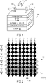
- FIG. 1 schematically shows a touch-sensitive display stack 100 configured to sense touch and hover input.
- display stack 100 includes an electrode matrix 102 above which a cover layer 104 is positioned.
- Cover layer 104 may be comprised of glass, plastic, or any other suitable material, and may protect display stack 100 from debris and forces while providing a surface 106 to which touch can be applied.
- Electrode matrix 102 includes a plurality of transmit (Tx) electrodes 112 and a plurality of receive (Rx) electrodes 110.
- Tx electrodes 112 and Rx electrodes 110 may be formed on two separate thin films as shown in FIG. 1 , and may be bonded together by an optically clear adhesive (OCA) not shown in FIG. 1 .
- OCA optically clear adhesive
- Other arrangements are possible, however, including those in which Tx electrodes 112 and Rx electrodes 110 are respectively formed on opposite sides of a single substrate, and those in which Tx electrodes 112 and Rx electrodes 110 are formed on a single layer along with jumpers arranged to electrically isolate the Tx and Rx electrodes. Turning briefly to FIG.
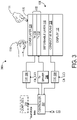
- an example electrode matrix 200 is shown, which includes Tx electrodes 112 and Rx electrodes 110 arranged in a diamond pattern.
- the example shown in FIG. 2 depicts eight rows of Tx electrodes 112 and eight columns of Rx electrodes 110, though any suitable number and arrangement are contemplated.
- Tx electrodes 112 and Rx electrodes 110 may be comprised of indium tin oxide (ITO), metal meshes, silver nanowires, or any other suitable materials.
- ITO indium tin oxide
- electrode matrix 102 may be selectively operated in a mutual capacitance mode or in a self-capacitance mode.
- touch input may be detected such as touch input from a human hand 111 and/or from an input object such as a stylus 114.
- hover input may be detected such as hover input from a hovering human hand 116.
- Touch-sensitive display stack 100 further includes a deformable layer 118 configured to resiliently deform in response to the application of force (e.g., applied to surface 106).
- Deformable layer 118 may be comprised of a soft silicone elastomer, urethane elastomer, acrylic film, or any other suitable material, and allows electrode matrix 102 to resiliently deflect toward a conductive plane 120, which, as described in further detail below, may facilitate a capacitive measurement of force.
- Conductive plane 120 may be comprised of a polymer film covered with ITO, a metal mesh, a silver nanowire dispersion, or any other suitable material/arrangement.
- conductive plane 120 may be a discrete layer separate from the other components in touch-sensitive display stack 100, while in other examples an existing layer in a display may be employed as the conductive plane.
- some liquid crystal displays (LCDs) include an ITO layer, which may shield the display from electromagnetic discharge, located on an exterior surface of a color filter plate. In this example, the display ITO layer may be employed as conductive plane 120.
- Touch-sensitive display stack 100 further includes a display 122 positioned at the bottom of the display stack.
- Display 122 may assume any suitable form (e.g., LCD, OLED, CRT) and may output graphical content for observation by users, which in some examples may be generated based on user input.
- display 122 is placed in a shielded position relative to conductive plane 120, which may shield the display from electromagnetic interference originating from electrode matrix 102, and the electrode matrix from electromagnetic interference originating from the display.
- Conductive plane 120 may cover substantially the entire area of display 122 (e.g., as viewed in a direction normal to surface 106). For examples in which display 122 includes an ITO layer, this ITO layer may be employed as conductive plane 120 in the manner described above.
- touch-sensitive display stack 100 may be operable to sense touch input, hover input including three-dimensional hand gestures, and applied force all via a common capacitive sensing mechanism. By consolidating these functions into a single stack, the cost and complexity of display stack 100 may be reduced relative to other approaches that employ different types of sensing mechanisms or multiple sensing mechanisms of a common type for different inputs.
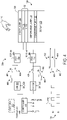
- FIG. 3 schematically depicts a touch-sensitive display device 300 incorporating touch-sensitive display stack 100 of FIG. 1 .
- FIG. 3 illustrates display device 300 configured to operate in a mutual capacitance mode.
- display device 300 may include other components not shown in FIG. 3 that are decoupled from the display device when operating in the mutual capacitance mode and coupled to the display device when operating in a self-capacitance mode.
- FIG. 6 illustrates circuitry that may be coupled to or decoupled from display device 300 depending on the selected mode.
- a mutual capacitance mode may be used to detect touch input applied to surface 106 of touch-sensitive display stack 100.
- a controller 302 may be configured to cause a Tx electrode driver 304 to drive Tx electrodes 112 in the mutual capacitance mode.
- Tx electrode driver 304 may sequentially apply AC voltages on each Tx electrode 112. Touch inputs may be detected based on resulting currents - e.g., that result from driving Tx electrodes 112 - induced on Rx electrodes 110.
- the resulting currents may be received by a current-to-digital (C2D) converter 306 where the currents may be digitized and provided as digital output to controller 302, which may then analyze the digital output to detect touch.
- C2D current-to-digital
- controller 302 may analyze the digital output to detect touch.
- the presence of human hand 111 or other touch objects may cause a decrease in the capacitance between Rx electrodes 110 and Tx electrodes 112, which may be reflected in the digital output from C2D 306 and received by controller 302.
- Detail regarding the configuration of an example C2D is provided below with reference to FIG. 7 .
- conductive plane 120 may facilitate a capacitive measurement of force in the mutual capacitance mode.
- conductive plane 120 may cooperate with electrode matrix 102 and deformable layer 118 to generate the capacitive measurement of force.
- electrode matrix 102 e.g., Tx electrodes 112
- Tx electrodes 112 may be configured to resiliently deflect relative to conductive plane 120 via the deformability of deformable layer 118.
- a C2D 308 coupled to conductive plane 120 may be configured to receive from the conductive plane this capacitive measurement of force, which can then be digitized and relayed to controller 302.
- the Tx electrodes and conductive plane may be charged to different voltages.
- Tx electrodes 112 may be sequentially driven with AC voltages.
- conductive plane 120 may be coupled to a reference voltage (e.g., fixed) at the input of C2D 308. This reference voltage may also be applied to the input of C2D 306 coupled to Rx electrodes 110.
- the reference voltage may be referred to as a 'common' reference voltage
- controller 302 may be configured to cause Rx electrodes 110 and conductive plane 120 to be connected to the common reference voltage in the mutual capacitance mode.
- an inner feedback loop of C2Ds 306 and 308 may maintain the input nodes of the C2Ds at the common reference voltage. Additional detail regarding the provision of the common reference voltage is described below with reference to FIG. 7 .
- the coupling of conductive plane 120 to the common reference voltage may provide electromagnetic shielding of display 122 as described above. Particularly, the charging of capacitors between electrode matrix 102 and display 122 may be prevented in this manner.
- conductive plane 120 may shield the electrode matrix (e.g., Rx electrodes 110) from electromagnetic interference from the display. In this way, the signal-to-noise ratio (SNR) of touch sensing may increase.
- SNR signal-to-noise ratio
- FIG. 3 illustrates the potential coupling of a computing device 310 to controller 302.
- controller 302 may provide touch and/or force data, including but not limited to an x-coordinate of touch, a y-coordinate of touch, and a magnitude of applied force.
- Computing device 310 may interpret such touch and/or force data as user input, and may render graphical content based thereon.
- FIG. 4 schematically depicts touch-sensitive display device 300 configured to operate in a self-capacitance mode. Components of display device 300 shown in FIG. 3 but not shown in FIG. 4 may be decoupled from the display device when operating in the self-capacitance mode.
- FIG. 6 illustrates circuitry that may be coupled to or decoupled from display device 300 depending on the selected mode.
- the self-capacitance mode may be engaged to detect hover input proximate surface 106 of touch-sensitive display stack 100.
- self-capacitances of Rx electrodes 110 and Tx electrodes 112 may be measured to detect hover input, as the measurement of self-capacitance may enable the detection of hover objects in a significantly greater range of z-distances from surface 106, relative to the z-distance range provided by the mutual capacitance mode.
- the detection of hover input may include determining x/y/z/ coordinates of a hover object and/or three-dimensional hand gestures performed, for example, by human hand 116.
- the self-capacitance mode may include charge periods that alternate with discharge periods, each of which may be enabled by actuating respective switches.
- controller 302 may be configured to cause Rx electrodes 110, Tx electrodes 112, and conductive plane 120 to be connected to a common charging voltage V charge during the charge periods by causing a plurality of ⁇ 1 switches 402 to close, which couples these elements of touch-sensitive display stack 100 to a fixed voltage source 403 providing V charge .
- controller 302 may be configured to cause Rx electrodes 110, Tx electrodes 112, and conductive plane 120 to be connected to a common reference voltage V ref during the discharge periods by causing switches 402 to open, and a plurality of ⁇ 2 switches 404 to close. As shown in FIG.
- the closing of switches 404 may cause coupling of Rx electrodes 110 and Tx electrodes 112 to the inputs of C2D 306 and a C2D 407, respectively, which as described above may be maintained at the common reference voltage via inner feedback loops.
- the closing of switches 404 may further cause coupling of conductive plane 120 to a fixed voltage source 406 providing the common reference voltage V ref . While shown as a discrete voltage source, fixed voltage source 406 may alternatively be implemented by providing the common reference voltage V ref at the input of C2D 308 as with C2Ds 306 and 407.
- the common reference voltage V ref provided to electrode matrix 102 and conductive plane 120 during the discharge periods may be the same as the common reference voltage provided to Rx electrodes 110 and the conductive plane in the mutual capacitance mode.
- controller 302 may be configured to cause Rx electrodes 110 and Tx electrodes 112 to be coupled to receive circuitry configured to measure the self-capacitances of the receive electrodes and the transmit electrodes. As shown in FIG.
- Rx electrodes 110 and Tx electrodes 112 may be respectively coupled to C2Ds 306 and 407, and consequently coupled to the common reference voltage V ref as described above.
- C2Ds 306 and 407 may respectively measure the self-capacitances of Rx electrodes 110 and Tx electrodes 112 - e.g., the charges stored on their respective self-capacitors C Rx_gnd V charge and C Tx_gnd V charge may be depleted by their corresponding C2Ds (e.g., to the extent that charges C Rx_gnd V ref and C Tx_gnd V ref respectively remain).
- the time-averaged currents sensed by C2Ds 306 and 407 may be C tx_gnd (V charge -V ref )/T clk_charge or C rx_gnd (V charge -V ref )/T clk_charge , respectively, where Tcik charge is the clock period of the charge and discharge periods.
- the charge and discharge periods may exhibit differing clock periods.
- FIG. 4 shows a timing diagram 408 illustrating clock signals ⁇ 1 and ⁇ 2 that may be used to drive the charge and discharge periods of the self-capacitance mode, respectively.
- the clock signals ⁇ 1 and ⁇ 2 may further represent the current and/or voltage through the switches respectively corresponding to the charge and discharge periods - e.g., through ⁇ 1 switches 402 during the charge periods and through ⁇ 2 switches 404 during the discharge periods.
- Timing diagram 408 illustrates how, in some implementations, the clock signals ⁇ 1 and ⁇ 2 may exhibit differing duty cycles (e.g., to support sufficient charging and accurate depletion).
- Rx electrodes 110 When implemented as an array of row and column electrodes, Rx electrodes 110 may be used to detect one of x-coordinate and y-coordinate motion of a hover object, and Tx electrodes 112 may be used to detect the other of the x-coordinate and y-coordinate motion.
- electrode matrix 200 illustrates an example arrangement of Rx electrodes 110 and Tx electrodes 112 in a rectangular array.
- the minimization of electrode overlap may be accomplished by minimizing a neck width 202.
- conductive plane 120 may be coupled to the common charge voltage V charge during charge periods of the self-capacitance mode and to the common reference voltage V ref during discharge periods.
- the conductive plane may provide an electromagnetic shielding function similar to the shielding function provided in the mutual capacitance mode. Further, charging of the capacitors between Rx electrodes 110 and conductive plane 120, and between Tx electrodes 112 and the conductive plane, can be avoided. These capacitances might otherwise be dominant in the measured self-capacitances, increasing the difficulty of detecting the relatively small capacitance changes introduced by hover object presence. In this manner the SNR of hover sensing may be increased.
- Controller 302 which may provide touch and/or force data as described above, may alternatively or additionally provide hover and/or gesture data to computing device 310.
- the hover and/or gesture data may include one or more of a hover object x-coordinate, y-coordinate, z-coordinate, and three-dimensional hand gesture.
- Computing device 310 may interpret such hover and/or gesture data as user input, and may render graphical content based thereon.
- FIG. 4 also illustrates how subsets of electrode matrix 102 may be multiplexed to achieve desired hover sensing conditions.
- the widths of Rx electrodes 110 and Tx electrodes 112 may be smaller than 1 cm to facilitate precise detection of the x/y position of touch input.
- the width / coverage area may be insufficient to form a detectable capacitance corresponding to hover objects such as human hand 116 positioned tens of centimeters away from surface 106.
- controller 302 may be configured to cause, in the self-capacitance mode, electrode subsets of Rx electrodes 110 and Tx electrodes 112 to be multiplexed together.
- Receive circuitry may be configured to measure the self-capacitance of each electrode subset.
- electrode multiplexing may be carried out by electrically coupling electrodes together.
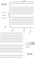
- FIG. 4 shows multiplexers 410 and 412 configured to multiplex electrodes of Rx electrodes 110 and Tx electrodes 112, respectively.
- FIG. 5A shows an example circuit 500 for multiplexing electrode subsets of an electrode array 502 together.
- Electrode array 502 may represent Rx electrodes 110 or Tx electrodes 112, for example, and comprises a plurality of electrodes that may be electrically coupled together by a multiplexer 504 to form k electrode subsets.
- Multiplexer 504 may be implemented as an array of switches or in any other suitable manner.
- Electrode array 502 may comprise any suitable number of electrodes, however, and any suitable number of electrode subsets may be formed, including subsets that differ in number.
- multiplexing electrode subsets of transmit and receive electrodes may include, for each subset, summing the measured self-capacitances of each electrode in that subset.
- FIG. 5B shows a circuit 506 for summing the self-capacitances of electrodes in electrode subsets of electrode array 502.
- receive circuitry - e.g., C2Ds such as C2D 508 - may be coupled to each electrode in electrode array 502.
- the outputs (e.g., measured self-capacitances) of the C2Ds 508 of each electrode in the subset may be summed to determine a total self-capacitance of that subset.
- any suitable number of electrode subsets may be formed by summing any suitable number of C2D outputs.
- C2D outputs may be summed at a summer 510, which may be implemented in controller 302, for example, or may be a component separate therefrom.
- Electrode multiplexing by summing C2D outputs may facilitate the omission of multiplexing hardware configured to electrically couple electrodes together, and may enable the output of capacitive data for every possible value of k in every frame (e.g., a complete scan of an electrode matrix).
- controller 302 may be configured to change a number of electrodes in electrode subsets over time - e.g., to change n or k to achieve a desired balance between x./y and z position sensing. In one example, controller 302 may be configured to change the number of electrodes in the electrode subsets based on a z-coordinate of an input object such as human hand 116.
- the z-coordinate may be determined based on the self-capacitance of Rx electrodes 110 and Tx electrodes 112 as described above.
- a larger or maximum number of electrodes may be multiplexed to maximize z resolution.
- the number of multiplexed electrodes may be reduced to increase x/y resolution.
- Alternative or additional approaches may consider the SNR of hover sensing - for example, when the SNR of the input object exceeds a threshold, the number of multiplexed electrodes may be reduced by 1, a factor of 2, or any other suitable integer.
- touch-sensitive display device 300 including circuitry that may be coupled to or decoupled from the display device depending on whether the mutual capacitance mode or the self-capacitance mode is selected.
- Coupled and decoupled can refer to a physical connection (e.g., operation of a transistor or other switching mechanism), and/or any other mechanism in which the circuitry componentry is selectively enabled or disabled with respect to providing a particular functionality.
- FIG. 6 illustrates how the selection of the mutual and self-capacitance modes may be effected by actuating respective switches.
- controller 302 may engage the mutual capacitance mode by actuating a plurality of Sel_mode switches 602, causing the coupling of Rx electrodes 110 to C2D 306, Tx electrodes 112 to Tx driver 304, and conductive plane 120 to C2D 308.
- the self-capacitance mode, and charge and discharge periods thereof, may be engaged by actuating ⁇ 1 switches 402 and ⁇ 2 switches 404 as described above.
- FIG. 6 further illustrates an example implementation of the receive circuitry of touch-sensitive display device 300.
- C2Ds 306, 308, and 407 may be collectively referred to as receive circuitry, as these elements may receive capacitive measurements in various modes.
- a respective C2D may be provided for each Rx electrode 110 and/or for each Tx electrode 112.
- C2Ds 306, 308, and 407 may employ different operational parameters in the mutual and self-capacitance modes, such as gain, processing algorithms, etc.
- FIG. 1 While FIG.
- FIG. 6 depicts the use of separate C2Ds 308 and 407 for receiving capacitive measurements from conductive plane 120 and Tx electrodes 112, respectively, in other implementations a consolidated C2D may be provided for these elements in combination with a switching mechanism.
- the consolidated C2D may be coupled to conductive plane 120 in the mutual capacitance mode and to Tx electrodes 112 in the self-capacitance mode.
- FIG. 6 illustrates how common receive circuitry can be used to implement mutual and self-capacitance modes and thereby detect both touch and hover input. This configuration may enable reduced cost and complexity relative to approaches that provide separate receive circuitry for touch and hover input detection.
- Controller 302 may be configured to switch between the mutual capacitance mode and the self-capacitance mode based on an input object condition. Switching between the mutual and self-capacitance modes may include interrupting the self-capacitance mode with the mutual capacitance mode at a first interval based on the input object condition.
- the mutual capacitance mode may not positively identify touch input - e.g., an input object in contact with surface 106. As such, it may be advisable to interrupt the self-capacitance mode with the mutual capacitance mode to capture touch inputs in a reasonable time frame.
- the first interval at which interruption occurs may be based on a z-coordinate of the input object such that, as the input object comes closer to surface 106 the first interval decreases - i.e., checks for touch input are performed more regularly, as touch input may be considered more likely the closer the input obj ect is to the surface. Conversely, checks for touch input may performed less regularly as the z-coordinate of the input object increases relative to surface 106, as touch input may be considered less likely the farther away the input object is from the surface.
- Switching between the mutual and self-capacitance modes may include interrupting the mutual capacitance mode with the self-capacitance mode at a second interval. It may be advisable, even when touch input is positively detected in the mutual capacitance mode, to interrupt (e.g., regularly) the mutual capacitance mode with the self-capacitance mode so that the presence of hover objects is identified in a reasonable time frame.
- both the mutual and self-capacitance modes may be leveraged to receive touch and hover input from the same user - e.g., as supplied by respective hands of the user. In other scenarios, both the mutual and self-capacitance modes may be leveraged to receive touch and hover input from different users.
- the second interval at which interruption of the mutual capacitance mode may occur may be predetermined or based on various suitable criteria (e.g., a probabilistic assessment of the likelihood of hover object presence, user preferences).
- a switch in sensing modes may occur if the SNR of input sensing decreases by a threshold amount or falls below a threshold level. Alternatively or additionally, if a minimum SNR is not detected for a threshold time, a switch in sensing modes may occur.
- various operational parameters may differ between modes - e.g., the mutual and self-capacitance modes may exhibit different drive frequencies and/or duty cycles.
- FIG. 7 schematically shows an example C2D circuit 700.
- Circuit 700 may be implemented by a sigma-delta convertor.
- the digital outputs D out ⁇ 0:n-1> and D out_b ⁇ 0:n-1>of an N-bit ADC may control the amount of current that should be steered into or out of the input node of a front-end integrator, so that the average current integrated on a capacitor Cint is 0.
- D out ⁇ 0:n-1> and D out_b ⁇ 0:n-1> may also be the outputs of the entire C2D, indicating the magnitude and direction of the input current.
- the N-bit ADC may be a single comparator or a latch, for example.
- the frequency of a clock signal clk C2D supplied to C2Ds may be much larger than the frequencies of the voltage signals applied by Tx driver 304 in touch mode and the frequencies of the charge and discharge clock cycles ⁇ 1 and ⁇ 2 in hover mode, for satisfactory SNR.
- Other variants of the sensor stacks and sensing electronics disclosed herein are possible without departing from the scope of this disclosure, however.
- Touch-sensitive display device 300 may employ receive circuitry comprising alternatives to the C2Ds described herein.
- the inner feedback loop of circuit 700 may maintain the input node at a fixed voltage during at least some portions of operation.
- Feedback current may be steered in or out of the negative input node of the first stage opamp (e.g., which may also be the input node of the C2D) to force voltage of the negative input node equal to that of the positive input node of the opamp which is connected to a fixed voltage source V ref .
- V ref may be zero.
- FIG. 8 shows a flowchart illustrating a method 800 of implementing a mutual capacitance mode and a self-capacitance mode in a touch-sensitive display device.
- Method 800 may be implemented in touch-sensitive display device 300 of FIG. 6 , for example.
- Method 800 includes, at 802, causing, at a controller in the touch-sensitive display device, a transmit electrode driver to drive a plurality of transmit electrodes in an electrode matrix in a mutual capacitance mode, and detecting touch inputs based on resulting currents on a plurality of receive electrodes in the electrode matrix.
- controller 302 of FIG. 6 may cause Tx driver 304 to drive Tx electrodes 112 in electrode matrix 102 in the mutual capacitance mode, and may detect touch inputs based on resulting currents on Rx electrodes 110 in the electrode matrix.
- Method 800 includes, at 804, causing the transmit electrodes, the receive electrodes, and a conductive plane to be connected to a common charging voltage during charge periods of a self-capacitance mode.
- controller 302 may cause Tx electrodes 112, Rx electrodes 110, and conductive plane 120 to be connected to the common charging voltage Vcharge (e.g., via coupling to voltage source 403 through actuation of switches 402) during charge periods of the self-capacitance mode.
- Method 800 includes, at 806, causing, during discharge periods of the self-capacitance mode that alternate with the charge periods, the transmit electrodes, the receive electrodes, and the conductive plane to be connected to a common reference voltage.
- controller 302 may cause, during the discharge periods of the self-capacitance mode that alternate with the charge periods, Tx electrodes 112, Rx electrodes 110, and conductive plane 120 to be connected to the common reference voltage V ref (e.g., via respective coupling to C2D 407, C2D 306, and C2D 308 through actuation of switches 404).
- Method 800 includes, at 808, causing, during the discharge periods of the self-capacitance mode, the transmit electrodes and the receive electrodes to be coupled to receive circuitry configured to measure self-capacitance of the transmit electrodes and the receive electrodes.
- controller 302 may cause, during the discharge periods of the self-capacitance mode, Tx electrodes 112 and Rx electrodes 110 to be coupled to receive circuitry (e.g., C2Ds 306, 308, 407) configured to measure self-capacitance of the transmit electrodes and the receive electrodes.
- One aspect provides a touch-sensitive display device, comprising an electrode matrix including a plurality of transmit electrodes and a plurality of receive electrodes; a conductive plane; a controller configured to cause a transmit electrode driver to drive the transmit electrodes in a mutual capacitance mode, with touch inputs being detected based on resulting currents on the receive electrodes; the controller configured to cause the transmit electrodes, the receive electrodes, and the conductive plane to be connected to a common charging voltage during charge periods of a self-capacitance mode; the controller configured, during discharge periods of the self-capacitance mode that alternate with the charge periods, to cause the transmit electrodes, the receive electrodes, and the conductive plane to be connected to a common reference voltage; and the controller configured, during the discharge periods of the self-capacitance mode, to cause the transmit electrodes and the receive electrodes to be coupled to receive circuitry configured to measure self-capacitance of the transmit electrodes and the receive electrodes.
- the receive circuitry may be configured to receive from the conductive plane a capacitive measurement of force applied to a surface of the touch-sensitive display device.
- at least a portion of the electrode matrix may be configured to resiliently deflect relative to the conductive plane, and the capacitive measurement of force may be measured between the resiliently deflecting portion of the electrode matrix and the conductive plane.
- the touch-sensitive display device may further comprise a display placed in a shielded position relative to the conductive plane, and the conductive plane may shield the display from electromagnetic interference from the electrode matrix and the electrode matrix from electromagnetic interference from the display.
- the controller may be configured to cause, in the self-capacitance mode, electrode subsets of the transmit electrodes and the receive electrodes to be multiplexed together, and the receive circuitry may be configured to measure a self-capacitance of each electrode subset.
- multiplexing the electrode subsets of the transmit electrodes and the receive electrodes may include electrically coupling electrodes together.
- multiplexing the electrode subsets of the transmit electrodes and the receive electrodes may include, for each electrode subset, summing self-capacitances of each electrode in that electrode subset.
- the controller may be configured to change a number of electrodes in the electrode subsets over time.
- the controller may be configured to change the number of electrodes in the electrode subsets based on a z-coordinate of an input object, and the z-coordinate may be determined based on the self-capacitance of the transmit electrodes and the receive electrodes.
- the controller may be configured to switch between the mutual capacitance mode and the self-capacitance mode based on an input object condition.
- the controller may be configured to enable each of the mutual capacitance mode, the charge periods of the self-capacitance mode, and the discharge periods of the self-capacitance mode by causing actuation of respective switches.
- the controller may be configured to, in the mutual capacitance mode, cause the conductive plane to be connected to the common reference voltage.
- a method at a controller in a touch-sensitive display device comprises causing a transmit electrode driver to drive a plurality of transmit electrodes in an electrode matrix in a mutual capacitance mode, and detecting touch inputs based on resulting currents on a plurality of receive electrodes in the electrode matrix; causing the transmit electrodes, the receive electrodes, and a conductive plane to be connected to a common charging voltage during charge periods of a self-capacitance mode; causing, during discharge periods of the self-capacitance mode that alternate with the charge periods, the transmit electrodes, the receive electrodes, and the conductive plane to be connected to a common reference voltage; and causing, during the discharge periods of the self-capacitance mode, the transmit electrodes and the receive electrodes to be coupled to receive circuitry configured to measure self-capacitance of the transmit electrodes and the receive electrodes.
- the method may comprise receiving from the conductive plane, via the receive circuitry, a capacitive measurement of force applied to a surface of the touch-sensitive display device.
- the method may comprise causing, in the self-capacitance mode, electrode subsets of the transmit electrodes and the receive electrodes to be multiplexed together; and measuring, via the receive circuitry, a self-capacitance of each electrode subset.
- the method may comprise changing a number of electrodes in the electrode subsets over time.
- the method may comprise changing the number of electrodes in the electrode subsets based on a z-coordinate of an input object, and the z-coordinate may be determined based on the self-capacitance of the transmit electrodes and the receive electrodes.
- the method may comprise switching between the mutual capacitance mode and the self-capacitance mode based on an input object condition.
- the input object condition may include a z-coordinate
- switching between the mutual capacitance mode and the self-capacitance mode based on the input object condition may include interrupting the self-capacitance mode with the mutual capacitance mode at a first interval based on the input object condition, and interrupting the mutual capacitance mode with the self-capacitance mode at a second interval.
- a touch-sensitive display device comprises an electrode matrix including a plurality of transmit electrodes and a plurality of receive electrodes; a conductive plane; a controller configured to cause a transmit electrode driver to drive the transmit electrodes in a mutual capacitance mode, with touch inputs being detected based on resulting currents on the receive electrodes; the controller configured to cause the transmit electrodes, the receive electrodes, and the conductive plane to be connected to a common charging voltage during charge periods of a self-capacitance mode; the controller configured, during discharge periods of the self-capacitance mode that alternate with the charge periods, to cause the transmit electrodes, the receive electrodes, and the conductive plane to be connected to a common reference voltage; and the controller configured, during the discharge periods of the self-capacitance mode, to cause the transmit electrodes and the receive electrodes to be coupled to receive circuitry configured to measure self-capacitance of the transmit electrodes and the receive electrodes, the receive circuitry further configured to receive from the conductive plane a capacitive measurement
Landscapes
- Engineering & Computer Science (AREA)
- General Engineering & Computer Science (AREA)
- Theoretical Computer Science (AREA)
- Physics & Mathematics (AREA)
- General Physics & Mathematics (AREA)
- Human Computer Interaction (AREA)
- Nonlinear Science (AREA)
- Mathematical Physics (AREA)
- Chemical & Material Sciences (AREA)
- Crystallography & Structural Chemistry (AREA)
- Optics & Photonics (AREA)
- Position Input By Displaying (AREA)
Description
- Various approaches to sensing touch and hover input have been developed. While some implementations only sense either touch or hover input, other implementations combine touch and hover sensing in a single device. A device configured to receive touch and hover input may sense touch input capacitively while sensing hover input with infrared image sensors, for example. Documents
US9151792 B1 US 2012/0050180 A1 andUS 2013/0257784 A1 relate to different types of touch sensitive display devices. -
-
FIG. 1 schematically shows a touch-sensitive display stack configured to sense touch and hover input. -
FIG. 2 shows an example electrode matrix. -
FIG. 3 schematically depicts a touch-sensitive display device incorporating the touch-sensitive display stack ofFIG. 1 , configured to operate in a mutual capacitance mode. -
FIG. 4 schematically depicts the touch-sensitive display device ofFIG. 3 , configured to operate in a self-capacitance mode. -
FIGS. 5A and 5B schematically illustrate electrode multiplexing in the touch-sensitive display device ofFIG. 3 . -
FIG. 6 schematically shows circuitry that may be coupled to the touch-sensitive display device ofFIG. 3 depending on a selection of the mutual and self-capacitance modes. -
FIG. 7 schematically shows an example C2D circuit. -
FIG. 8 shows a flowchart illustrating a method of implementing a mutual capacitance mode and a self-capacitance mode in a touch-sensitive display device. - The invention is as set out in the independent claims, further aspects of the invention are outlined in the dependent claims. Embodiments that do not fall within the scope of the claims do not describe part of the invention. As described above, a variety of approaches have been developed for sensing touch and hover input in relation to the user-facing surface of computing devices. While some implementations can only sense one type, other implementations combine touch and hover sensing in a single device. For example, a device configured for both touch and hover sensing may employ capacitive sensing (e.g., via an electrode matrix) to receive touch input, and (e.g., infrared) image sensors to receive hover input. The use of capacitive and imagebased sensing mechanisms to respectively receive touch and hover input, however, increases device cost and complexity. For some devices, this may be compounded by the inclusion of multiple image sensors for sensing hover over substantially the entirety of an input surface. Other devices may increase cost and complexity by providing separate sensors for detecting touch and measuring force, respectively.
- To address these and other issues, implementations of a touch-sensitive display device operable to sense touch and hover input are disclosed herein. As described below, capacitive sensing may be used to receive both touch and hover input, among other inputs such as force measurements and three-dimensional hand gestures.
-
FIG. 1 schematically shows a touch-sensitive display stack 100 configured to sense touch and hover input. To this end,display stack 100 includes anelectrode matrix 102 above which acover layer 104 is positioned.Cover layer 104 may be comprised of glass, plastic, or any other suitable material, and may protectdisplay stack 100 from debris and forces while providing asurface 106 to which touch can be applied. -
Electrode matrix 102 includes a plurality of transmit (Tx)electrodes 112 and a plurality of receive (Rx)electrodes 110. In one example,Tx electrodes 112 andRx electrodes 110 may be formed on two separate thin films as shown inFIG. 1 , and may be bonded together by an optically clear adhesive (OCA) not shown inFIG. 1 . Other arrangements are possible, however, including those in whichTx electrodes 112 andRx electrodes 110 are respectively formed on opposite sides of a single substrate, and those in whichTx electrodes 112 andRx electrodes 110 are formed on a single layer along with jumpers arranged to electrically isolate the Tx and Rx electrodes. Turning briefly toFIG. 2 , anexample electrode matrix 200 is shown, which includesTx electrodes 112 andRx electrodes 110 arranged in a diamond pattern. The example shown inFIG. 2 depicts eight rows ofTx electrodes 112 and eight columns ofRx electrodes 110, though any suitable number and arrangement are contemplated.Tx electrodes 112 andRx electrodes 110 may be comprised of indium tin oxide (ITO), metal meshes, silver nanowires, or any other suitable materials. - As described in further detail below,
electrode matrix 102 may be selectively operated in a mutual capacitance mode or in a self-capacitance mode. In the mutual capacitance mode, touch input may be detected such as touch input from ahuman hand 111 and/or from an input object such as astylus 114. In the self-capacitance mode, hover input may be detected such as hover input from a hoveringhuman hand 116. - Touch-
sensitive display stack 100 further includes adeformable layer 118 configured to resiliently deform in response to the application of force (e.g., applied to surface 106).Deformable layer 118 may be comprised of a soft silicone elastomer, urethane elastomer, acrylic film, or any other suitable material, and allowselectrode matrix 102 to resiliently deflect toward aconductive plane 120, which, as described in further detail below, may facilitate a capacitive measurement of force. -
Conductive plane 120 may be comprised of a polymer film covered with ITO, a metal mesh, a silver nanowire dispersion, or any other suitable material/arrangement. In some implementations,conductive plane 120 may be a discrete layer separate from the other components in touch-sensitive display stack 100, while in other examples an existing layer in a display may be employed as the conductive plane. For example, some liquid crystal displays (LCDs) include an ITO layer, which may shield the display from electromagnetic discharge, located on an exterior surface of a color filter plate. In this example, the display ITO layer may be employed asconductive plane 120. - Touch-
sensitive display stack 100 further includes adisplay 122 positioned at the bottom of the display stack.Display 122 may assume any suitable form (e.g., LCD, OLED, CRT) and may output graphical content for observation by users, which in some examples may be generated based on user input. As described in further detail below,display 122 is placed in a shielded position relative toconductive plane 120, which may shield the display from electromagnetic interference originating fromelectrode matrix 102, and the electrode matrix from electromagnetic interference originating from the display.Conductive plane 120 may cover substantially the entire area of display 122 (e.g., as viewed in a direction normal to surface 106). For examples in whichdisplay 122 includes an ITO layer, this ITO layer may be employed asconductive plane 120 in the manner described above. - In view of the above, touch-
sensitive display stack 100 may be operable to sense touch input, hover input including three-dimensional hand gestures, and applied force all via a common capacitive sensing mechanism. By consolidating these functions into a single stack, the cost and complexity ofdisplay stack 100 may be reduced relative to other approaches that employ different types of sensing mechanisms or multiple sensing mechanisms of a common type for different inputs. -
FIG. 3 schematically depicts a touch-sensitive display device 300 incorporating touch-sensitive display stack 100 ofFIG. 1 . In particular,FIG. 3 illustratesdisplay device 300 configured to operate in a mutual capacitance mode. As described in further detail below with reference toFIG. 4 ,display device 300 may include other components not shown inFIG. 3 that are decoupled from the display device when operating in the mutual capacitance mode and coupled to the display device when operating in a self-capacitance mode.FIG. 6 illustrates circuitry that may be coupled to or decoupled fromdisplay device 300 depending on the selected mode. - As described above, a mutual capacitance mode may be used to detect touch input applied to
surface 106 of touch-sensitive display stack 100. To facilitate operation in the mutual capacitance mode, acontroller 302 may be configured to cause aTx electrode driver 304 to driveTx electrodes 112 in the mutual capacitance mode. In one example,Tx electrode driver 304 may sequentially apply AC voltages on eachTx electrode 112. Touch inputs may be detected based on resulting currents - e.g., that result from driving Tx electrodes 112 - induced onRx electrodes 110. The resulting currents may be received by a current-to-digital (C2D)converter 306 where the currents may be digitized and provided as digital output tocontroller 302, which may then analyze the digital output to detect touch. The presence ofhuman hand 111 or other touch objects may cause a decrease in the capacitance betweenRx electrodes 110 andTx electrodes 112, which may be reflected in the digital output fromC2D 306 and received bycontroller 302. Detail regarding the configuration of an example C2D is provided below with reference toFIG. 7 . - As described above,
conductive plane 120 may facilitate a capacitive measurement of force in the mutual capacitance mode. To this end,conductive plane 120 may cooperate withelectrode matrix 102 anddeformable layer 118 to generate the capacitive measurement of force. In response to the application of force tosurface 106, at least a portion of electrode matrix 102 (e.g., Tx electrodes 112) may be configured to resiliently deflect relative toconductive plane 120 via the deformability ofdeformable layer 118. Asdeformable layer 118 is compressed, the distance betweenelectrode matrix 102 andconductive plane 120 changes, in turn increasing the capacitance between the electrode matrix and conductive plane. As such, the capacitive measurement of force may be measured between the resiliently deflecting portion ofelectrode matrix 102 andconductive plane 120. AC2D 308 coupled toconductive plane 120 may be configured to receive from the conductive plane this capacitive measurement of force, which can then be digitized and relayed tocontroller 302. - To charge the capacitor between electrode matrix 102 (e.g., Tx electrodes 112) and
conductive plane 120, and thus enable force measurement based on changes in the value of the capacitor, the Tx electrodes and conductive plane may be charged to different voltages. As described above,Tx electrodes 112 may be sequentially driven with AC voltages. In addition,conductive plane 120 may be coupled to a reference voltage (e.g., fixed) at the input ofC2D 308. This reference voltage may also be applied to the input ofC2D 306 coupled toRx electrodes 110. As such, the reference voltage may be referred to as a 'common' reference voltage, andcontroller 302 may be configured to causeRx electrodes 110 andconductive plane 120 to be connected to the common reference voltage in the mutual capacitance mode. To provide the common reference voltage, an inner feedback loop ofC2Ds FIG. 7 . - The coupling of
conductive plane 120 to the common reference voltage may provide electromagnetic shielding ofdisplay 122 as described above. Particularly, the charging of capacitors betweenelectrode matrix 102 anddisplay 122 may be prevented in this manner. In addition to shieldingdisplay 122 from electromagnetic interference (e.g., from Tx electrodes 112),conductive plane 120 may shield the electrode matrix (e.g., Rx electrodes 110) from electromagnetic interference from the display. In this way, the signal-to-noise ratio (SNR) of touch sensing may increase. -
FIG. 3 illustrates the potential coupling of acomputing device 310 tocontroller 302. As shown therein,controller 302 may provide touch and/or force data, including but not limited to an x-coordinate of touch, a y-coordinate of touch, and a magnitude of applied force.Computing device 310 may interpret such touch and/or force data as user input, and may render graphical content based thereon. -
FIG. 4 schematically depicts touch-sensitive display device 300 configured to operate in a self-capacitance mode. Components ofdisplay device 300 shown inFIG. 3 but not shown inFIG. 4 may be decoupled from the display device when operating in the self-capacitance mode.FIG. 6 illustrates circuitry that may be coupled to or decoupled fromdisplay device 300 depending on the selected mode. - As described above, the self-capacitance mode may be engaged to detect hover input
proximate surface 106 of touch-sensitive display stack 100. In contrast to the mutual capacitance mode, self-capacitances ofRx electrodes 110 andTx electrodes 112 may be measured to detect hover input, as the measurement of self-capacitance may enable the detection of hover objects in a significantly greater range of z-distances fromsurface 106, relative to the z-distance range provided by the mutual capacitance mode. The detection of hover input may include determining x/y/z/ coordinates of a hover object and/or three-dimensional hand gestures performed, for example, byhuman hand 116. - The self-capacitance mode may include charge periods that alternate with discharge periods, each of which may be enabled by actuating respective switches. In particular,
controller 302 may be configured to causeRx electrodes 110,Tx electrodes 112, andconductive plane 120 to be connected to a common charging voltage Vcharge during the charge periods by causing a plurality of ϕ1 switches 402 to close, which couples these elements of touch-sensitive display stack 100 to a fixedvoltage source 403 providing Vcharge. Conversely,controller 302 may be configured to causeRx electrodes 110,Tx electrodes 112, andconductive plane 120 to be connected to a common reference voltage Vref during the discharge periods by causingswitches 402 to open, and a plurality of ϕ2 switches 404 to close. As shown inFIG. 4 , the closing ofswitches 404 may cause coupling ofRx electrodes 110 andTx electrodes 112 to the inputs ofC2D 306 and aC2D 407, respectively, which as described above may be maintained at the common reference voltage via inner feedback loops. The closing ofswitches 404 may further cause coupling ofconductive plane 120 to a fixedvoltage source 406 providing the common reference voltage Vref. While shown as a discrete voltage source, fixedvoltage source 406 may alternatively be implemented by providing the common reference voltage Vref at the input ofC2D 308 as withC2Ds electrode matrix 102 andconductive plane 120 during the discharge periods may be the same as the common reference voltage provided toRx electrodes 110 and the conductive plane in the mutual capacitance mode. - During the charge periods, charges of magnitude CRx_gndVcharge and CTx_gndVcharge may be stored on the self-capacitors of
Rx electrodes 110 andTx electrodes 112, respectively, where CRx, gnd and CTx, gnd are the respective self-capacitances of the Rx and Tx electrodes. During the discharge periods of the self-capacitance mode,controller 302 may be configured to causeRx electrodes 110 andTx electrodes 112 to be coupled to receive circuitry configured to measure the self-capacitances of the receive electrodes and the transmit electrodes. As shown inFIG. 4 , by closingswitches 404 as described above,Rx electrodes 110 andTx electrodes 112 may be respectively coupled to C2Ds 306 and 407, and consequently coupled to the common reference voltage Vref as described above.C2Ds Rx electrodes 110 and Tx electrodes 112 - e.g., the charges stored on their respective self-capacitors CRx_gndVcharge and CTx_gndVcharge may be depleted by their corresponding C2Ds (e.g., to the extent that charges CRx_gndVref and CTx_gndVref respectively remain). The time-averaged currents sensed byC2Ds -
FIG. 4 shows a timing diagram 408 illustrating clock signals ϕ1 and ϕ2 that may be used to drive the charge and discharge periods of the self-capacitance mode, respectively. The clock signals ϕ1 and ϕ2 may further represent the current and/or voltage through the switches respectively corresponding to the charge and discharge periods - e.g., through ϕ1 switches 402 during the charge periods and through ϕ2 switches 404 during the discharge periods. Timing diagram 408 illustrates how, in some implementations, the clock signals ϕ1 and ϕ2 may exhibit differing duty cycles (e.g., to support sufficient charging and accurate depletion). - When implemented as an array of row and column electrodes,
Rx electrodes 110 may be used to detect one of x-coordinate and y-coordinate motion of a hover object, andTx electrodes 112 may be used to detect the other of the x-coordinate and y-coordinate motion. Returning briefly toFIG. 2 ,electrode matrix 200 illustrates an example arrangement ofRx electrodes 110 andTx electrodes 112 in a rectangular array. When a hover object hovers aboveRx electrodes 110 andTx electrodes 112, the self-capacitances of the electrodes may increase, enabling the x, y, and z coordinates of the hover object to be sensed. To enable a similar sensing resolution of the z-coordinate when the hover object moves in the x or y direction, it may be desired to minimize the area whereRx electrodes 110 andTx electrodes 112 overlap. In this way, the degree to which electrodes (e.g., Tx electrodes 112) farther away from the hover object are shielded by electrodes (e.g., Rx electrodes 110) closer to the hover object may be minimized. As one example, the minimization of electrode overlap may be accomplished by minimizing aneck width 202. - Returning to
FIG. 4 ,conductive plane 120 may be coupled to the common charge voltage Vcharge during charge periods of the self-capacitance mode and to the common reference voltage Vref during discharge periods. By applying this electrical coupling toconductive plane 120 and toelectrode matrix 102 in the self-capacitance mode, the conductive plane may provide an electromagnetic shielding function similar to the shielding function provided in the mutual capacitance mode. Further, charging of the capacitors betweenRx electrodes 110 andconductive plane 120, and betweenTx electrodes 112 and the conductive plane, can be avoided. These capacitances might otherwise be dominant in the measured self-capacitances, increasing the difficulty of detecting the relatively small capacitance changes introduced by hover object presence. In this manner the SNR of hover sensing may be increased. -
Controller 302, which may provide touch and/or force data as described above, may alternatively or additionally provide hover and/or gesture data tocomputing device 310. As described above, the hover and/or gesture data may include one or more of a hover object x-coordinate, y-coordinate, z-coordinate, and three-dimensional hand gesture.Computing device 310 may interpret such hover and/or gesture data as user input, and may render graphical content based thereon. -
FIG. 4 also illustrates how subsets ofelectrode matrix 102 may be multiplexed to achieve desired hover sensing conditions. In some examples, the widths ofRx electrodes 110 andTx electrodes 112 may be smaller than 1 cm to facilitate precise detection of the x/y position of touch input. However, the width / coverage area may be insufficient to form a detectable capacitance corresponding to hover objects such ashuman hand 116 positioned tens of centimeters away fromsurface 106. As such,controller 302 may be configured to cause, in the self-capacitance mode, electrode subsets ofRx electrodes 110 andTx electrodes 112 to be multiplexed together. Receive circuitry may be configured to measure the self-capacitance of each electrode subset. - In some implementations, electrode multiplexing may be carried out by electrically coupling electrodes together. To this end,
FIG. 4 showsmultiplexers Rx electrodes 110 andTx electrodes 112, respectively. As further detail regarding multiplexing,FIG. 5A shows anexample circuit 500 for multiplexing electrode subsets of anelectrode array 502 together.Electrode array 502 may representRx electrodes 110 orTx electrodes 112, for example, and comprises a plurality of electrodes that may be electrically coupled together by amultiplexer 504 to form k electrode subsets.Multiplexer 504 may be implemented as an array of switches or in any other suitable manner. In particular, an integer number n of electrodes may be electrically coupled together to form k subsets; in the example depicted inFIGS. 5A and 5B ,2 grouped electrodes forms 8 subsets, 4 grouped electrodes forms 4 subsets, 8 grouped electrodes forms 2 subsets, 16 grouped electrodes forms 1 subset, etc.Electrode array 502 may comprise any suitable number of electrodes, however, and any suitable number of electrode subsets may be formed, including subsets that differ in number. - In other implementations, multiplexing electrode subsets of transmit and receive electrodes may include, for each subset, summing the measured self-capacitances of each electrode in that subset. To this end,
FIG. 5B shows acircuit 506 for summing the self-capacitances of electrodes in electrode subsets ofelectrode array 502. In this example, receive circuitry - e.g., C2Ds such as C2D 508 - may be coupled to each electrode inelectrode array 502. For each electrode subset, the outputs (e.g., measured self-capacitances) of theC2Ds 508 of each electrode in the subset may be summed to determine a total self-capacitance of that subset. As withcircuit 500, any suitable number of electrode subsets may be formed by summing any suitable number of C2D outputs. C2D outputs may be summed at a summer 510, which may be implemented incontroller 302, for example, or may be a component separate therefrom. Electrode multiplexing by summing C2D outputs may facilitate the omission of multiplexing hardware configured to electrically couple electrodes together, and may enable the output of capacitive data for every possible value of k in every frame (e.g., a complete scan of an electrode matrix). - Returning to
FIG. 4 , greater values of n (i.e., greater numbers of multiplexed electrodes) may enable hover sensing in a greater range of z-distances fromsurface 106. However, as n increased, the resolution of x/y position sensing may decrease. As such,controller 302 may be configured to change a number of electrodes in electrode subsets over time - e.g., to change n or k to achieve a desired balance between x./y and z position sensing. In one example,controller 302 may be configured to change the number of electrodes in the electrode subsets based on a z-coordinate of an input object such ashuman hand 116. The z-coordinate may be determined based on the self-capacitance ofRx electrodes 110 andTx electrodes 112 as described above. In this example, upon initiation of the self-capacitance mode, a larger or maximum number of electrodes may be multiplexed to maximize z resolution. As the input object comes closer to surface 106, the number of multiplexed electrodes may be reduced to increase x/y resolution. Alternative or additional approaches may consider the SNR of hover sensing - for example, when the SNR of the input object exceeds a threshold, the number of multiplexed electrodes may be reduced by 1, a factor of 2, or any other suitable integer. - Turning now to
FIG. 6 , touch-sensitive display device 300 is shown including circuitry that may be coupled to or decoupled from the display device depending on whether the mutual capacitance mode or the self-capacitance mode is selected. "Coupled" and "decoupled," as used herein, can refer to a physical connection (e.g., operation of a transistor or other switching mechanism), and/or any other mechanism in which the circuitry componentry is selectively enabled or disabled with respect to providing a particular functionality. -
FIG. 6 illustrates how the selection of the mutual and self-capacitance modes may be effected by actuating respective switches. In particular,controller 302 may engage the mutual capacitance mode by actuating a plurality of Sel_mode switches 602, causing the coupling ofRx electrodes 110 toC2D 306,Tx electrodes 112 toTx driver 304, andconductive plane 120 toC2D 308. The self-capacitance mode, and charge and discharge periods thereof, may be engaged by actuating ϕ1 switches 402 and ϕ2 switches 404 as described above. -
FIG. 6 further illustrates an example implementation of the receive circuitry of touch-sensitive display device 300. In the depicted example,C2Ds Rx electrode 110 and/or for eachTx electrode 112.C2Ds FIG. 6 depicts the use ofseparate C2Ds conductive plane 120 andTx electrodes 112, respectively, in other implementations a consolidated C2D may be provided for these elements in combination with a switching mechanism. The consolidated C2D may be coupled toconductive plane 120 in the mutual capacitance mode and toTx electrodes 112 in the self-capacitance mode. Regardless,FIG. 6 illustrates how common receive circuitry can be used to implement mutual and self-capacitance modes and thereby detect both touch and hover input. This configuration may enable reduced cost and complexity relative to approaches that provide separate receive circuitry for touch and hover input detection. -
Controller 302 may be configured to switch between the mutual capacitance mode and the self-capacitance mode based on an input object condition. Switching between the mutual and self-capacitance modes may include interrupting the self-capacitance mode with the mutual capacitance mode at a first interval based on the input object condition. In some examples, the mutual capacitance mode may not positively identify touch input - e.g., an input object in contact withsurface 106. As such, it may be advisable to interrupt the self-capacitance mode with the mutual capacitance mode to capture touch inputs in a reasonable time frame. The first interval at which interruption occurs may be based on a z-coordinate of the input object such that, as the input object comes closer to surface 106 the first interval decreases - i.e., checks for touch input are performed more regularly, as touch input may be considered more likely the closer the input obj ect is to the surface. Conversely, checks for touch input may performed less regularly as the z-coordinate of the input object increases relative tosurface 106, as touch input may be considered less likely the farther away the input object is from the surface. - Switching between the mutual and self-capacitance modes may include interrupting the mutual capacitance mode with the self-capacitance mode at a second interval. It may be advisable, even when touch input is positively detected in the mutual capacitance mode, to interrupt (e.g., regularly) the mutual capacitance mode with the self-capacitance mode so that the presence of hover objects is identified in a reasonable time frame. In some scenarios, both the mutual and self-capacitance modes may be leveraged to receive touch and hover input from the same user - e.g., as supplied by respective hands of the user. In other scenarios, both the mutual and self-capacitance modes may be leveraged to receive touch and hover input from different users. The second interval at which interruption of the mutual capacitance mode may occur may be predetermined or based on various suitable criteria (e.g., a probabilistic assessment of the likelihood of hover object presence, user preferences).
- Other considerations may drive switches between the mutual and self-capacitance modes. For example, if the SNR of input sensing decreases by a threshold amount or falls below a threshold level, a switch in sensing modes may occur. Alternatively or additionally, if a minimum SNR is not detected for a threshold time, a switch in sensing modes may occur. In some implementations, various operational parameters may differ between modes - e.g., the mutual and self-capacitance modes may exhibit different drive frequencies and/or duty cycles.
-
FIG. 7 schematically shows anexample C2D circuit 700.Circuit 700 may be implemented by a sigma-delta convertor. The digital outputs Dout<0:n-1> and Dout_b<0:n-1>of an N-bit ADC may control the amount of current that should be steered into or out of the input node of a front-end integrator, so that the average current integrated on a capacitor Cint is 0. Dout<0:n-1> and Dout_b<0:n-1> may also be the outputs of the entire C2D, indicating the magnitude and direction of the input current. The N-bit ADC may be a single comparator or a latch, for example. The frequency of a clock signal clk C2D supplied to C2Ds (e.g.,C2Ds Tx driver 304 in touch mode and the frequencies of the charge and discharge clock cycles ϕ1 and ϕ2 in hover mode, for satisfactory SNR. Other variants of the sensor stacks and sensing electronics disclosed herein are possible without departing from the scope of this disclosure, however. Touch-sensitive display device 300 (FIG. 6 ), for example, may employ receive circuitry comprising alternatives to the C2Ds described herein. - The inner feedback loop of
circuit 700 may maintain the input node at a fixed voltage during at least some portions of operation. Feedback current may be steered in or out of the negative input node of the first stage opamp (e.g., which may also be the input node of the C2D) to force voltage of the negative input node equal to that of the positive input node of the opamp which is connected to a fixed voltage source Vref. In some cases, Vref may be zero. -
FIG. 8 shows a flowchart illustrating amethod 800 of implementing a mutual capacitance mode and a self-capacitance mode in a touch-sensitive display device.Method 800 may be implemented in touch-sensitive display device 300 ofFIG. 6 , for example. -
Method 800 includes, at 802, causing, at a controller in the touch-sensitive display device, a transmit electrode driver to drive a plurality of transmit electrodes in an electrode matrix in a mutual capacitance mode, and detecting touch inputs based on resulting currents on a plurality of receive electrodes in the electrode matrix. For example,controller 302 ofFIG. 6 may causeTx driver 304 to driveTx electrodes 112 inelectrode matrix 102 in the mutual capacitance mode, and may detect touch inputs based on resulting currents onRx electrodes 110 in the electrode matrix. -
Method 800 includes, at 804, causing the transmit electrodes, the receive electrodes, and a conductive plane to be connected to a common charging voltage during charge periods of a self-capacitance mode. For example,controller 302 may causeTx electrodes 112,Rx electrodes 110, andconductive plane 120 to be connected to the common charging voltage Vcharge (e.g., via coupling tovoltage source 403 through actuation of switches 402) during charge periods of the self-capacitance mode. -
Method 800 includes, at 806, causing, during discharge periods of the self-capacitance mode that alternate with the charge periods, the transmit electrodes, the receive electrodes, and the conductive plane to be connected to a common reference voltage. For example,controller 302 may cause, during the discharge periods of the self-capacitance mode that alternate with the charge periods,Tx electrodes 112,Rx electrodes 110, andconductive plane 120 to be connected to the common reference voltage Vref (e.g., via respective coupling toC2D 407,C2D 306, andC2D 308 through actuation of switches 404). -
Method 800 includes, at 808, causing, during the discharge periods of the self-capacitance mode, the transmit electrodes and the receive electrodes to be coupled to receive circuitry configured to measure self-capacitance of the transmit electrodes and the receive electrodes. For example,controller 302 may cause, during the discharge periods of the self-capacitance mode,Tx electrodes 112 andRx electrodes 110 to be coupled to receive circuitry (e.g.,C2Ds - The subject matter of the present disclosure is further described in the following paragraphs. One aspect provides a touch-sensitive display device, comprising an electrode matrix including a plurality of transmit electrodes and a plurality of receive electrodes; a conductive plane; a controller configured to cause a transmit electrode driver to drive the transmit electrodes in a mutual capacitance mode, with touch inputs being detected based on resulting currents on the receive electrodes; the controller configured to cause the transmit electrodes, the receive electrodes, and the conductive plane to be connected to a common charging voltage during charge periods of a self-capacitance mode; the controller configured, during discharge periods of the self-capacitance mode that alternate with the charge periods, to cause the transmit electrodes, the receive electrodes, and the conductive plane to be connected to a common reference voltage; and the controller configured, during the discharge periods of the self-capacitance mode, to cause the transmit electrodes and the receive electrodes to be coupled to receive circuitry configured to measure self-capacitance of the transmit electrodes and the receive electrodes. In this aspect, the receive circuitry may be configured to receive from the conductive plane a capacitive measurement of force applied to a surface of the touch-sensitive display device. In this aspect, at least a portion of the electrode matrix may be configured to resiliently deflect relative to the conductive plane, and the capacitive measurement of force may be measured between the resiliently deflecting portion of the electrode matrix and the conductive plane. In this aspect, the touch-sensitive display device may further comprise a display placed in a shielded position relative to the conductive plane, and the conductive plane may shield the display from electromagnetic interference from the electrode matrix and the electrode matrix from electromagnetic interference from the display. In this aspect, the controller may be configured to cause, in the self-capacitance mode, electrode subsets of the transmit electrodes and the receive electrodes to be multiplexed together, and the receive circuitry may be configured to measure a self-capacitance of each electrode subset. In this aspect, multiplexing the electrode subsets of the transmit electrodes and the receive electrodes may include electrically coupling electrodes together. In this aspect, multiplexing the electrode subsets of the transmit electrodes and the receive electrodes may include, for each electrode subset, summing self-capacitances of each electrode in that electrode subset. In this aspect, the controller may be configured to change a number of electrodes in the electrode subsets over time. In this aspect, the controller may be configured to change the number of electrodes in the electrode subsets based on a z-coordinate of an input object, and the z-coordinate may be determined based on the self-capacitance of the transmit electrodes and the receive electrodes. In this aspect, the controller may be configured to switch between the mutual capacitance mode and the self-capacitance mode based on an input object condition. In this aspect, the controller may be configured to enable each of the mutual capacitance mode, the charge periods of the self-capacitance mode, and the discharge periods of the self-capacitance mode by causing actuation of respective switches. In this aspect, the controller may be configured to, in the mutual capacitance mode, cause the conductive plane to be connected to the common reference voltage.
- According to another aspect, a method at a controller in a touch-sensitive display device comprises causing a transmit electrode driver to drive a plurality of transmit electrodes in an electrode matrix in a mutual capacitance mode, and detecting touch inputs based on resulting currents on a plurality of receive electrodes in the electrode matrix; causing the transmit electrodes, the receive electrodes, and a conductive plane to be connected to a common charging voltage during charge periods of a self-capacitance mode; causing, during discharge periods of the self-capacitance mode that alternate with the charge periods, the transmit electrodes, the receive electrodes, and the conductive plane to be connected to a common reference voltage; and causing, during the discharge periods of the self-capacitance mode, the transmit electrodes and the receive electrodes to be coupled to receive circuitry configured to measure self-capacitance of the transmit electrodes and the receive electrodes. In this aspect, the method may comprise receiving from the conductive plane, via the receive circuitry, a capacitive measurement of force applied to a surface of the touch-sensitive display device. In this aspect, the method may comprise causing, in the self-capacitance mode, electrode subsets of the transmit electrodes and the receive electrodes to be multiplexed together; and measuring, via the receive circuitry, a self-capacitance of each electrode subset. In this aspect, the method may comprise changing a number of electrodes in the electrode subsets over time. In this aspect, the method may comprise changing the number of electrodes in the electrode subsets based on a z-coordinate of an input object, and the z-coordinate may be determined based on the self-capacitance of the transmit electrodes and the receive electrodes. In this aspect, the method may comprise switching between the mutual capacitance mode and the self-capacitance mode based on an input object condition. In this aspect, the input object condition may include a z-coordinate, and switching between the mutual capacitance mode and the self-capacitance mode based on the input object condition may include interrupting the self-capacitance mode with the mutual capacitance mode at a first interval based on the input object condition, and interrupting the mutual capacitance mode with the self-capacitance mode at a second interval.
- According to another aspect, a touch-sensitive display device comprises an electrode matrix including a plurality of transmit electrodes and a plurality of receive electrodes; a conductive plane; a controller configured to cause a transmit electrode driver to drive the transmit electrodes in a mutual capacitance mode, with touch inputs being detected based on resulting currents on the receive electrodes; the controller configured to cause the transmit electrodes, the receive electrodes, and the conductive plane to be connected to a common charging voltage during charge periods of a self-capacitance mode; the controller configured, during discharge periods of the self-capacitance mode that alternate with the charge periods, to cause the transmit electrodes, the receive electrodes, and the conductive plane to be connected to a common reference voltage; and the controller configured, during the discharge periods of the self-capacitance mode, to cause the transmit electrodes and the receive electrodes to be coupled to receive circuitry configured to measure self-capacitance of the transmit electrodes and the receive electrodes, the receive circuitry further configured to receive from the conductive plane a capacitive measurement of force applied to a surface of the touch-sensitive display device.
- It will be understood that the configurations and/or approaches described herein are exemplary in nature, and that these specific embodiments or examples are not to be considered in a limiting sense, because numerous variations are possible. The specific routines or methods described herein may represent one or more of any number of processing strategies. As such, various acts illustrated and/or described may be performed in the sequence illustrated and/or described, in other sequences, in parallel, or omitted. Likewise, the order of the above-described processes may be changed.
- The subject matter of the present disclosure includes all novel and nonobvious combinations and subcombinations of the various processes, systems and configurations, and other features, functions, acts, and/or properties disclosed herein.
Claims (11)
- A touch-sensitive display device (100; 300), comprising:an electrode matrix (102) including a plurality of transmit electrodes (112) and a plurality of receive electrodes (110);a conductive plane (120);a transmit electrode driver (304);a receive circuitry;a controller(302) configured to cause the transmit electrode driver (304) to drive the transmit electrodes (112) in a mutual capacitance mode, with touch inputs being detected based on resulting currents on the receive electrodes (110);the controller (302) configured to cause the transmit electrodes (112), the receive electrodes (110), and the conductive plane (120) to be connected to a common charging voltage during charge periods of a self-capacitance mode;the controller (302) configured, during discharge periods of the self-capacitance mode that alternate with the charge periods, to cause the transmit electrodes (112), the receive electrodes (110), and the conductive plane (120) to be connected to a common reference voltage ref; andthe controller (302) configured, during the discharge periods of the self-capacitance mode, to cause the transmit electrodes (112) and the receive electrodes (110) to be coupled to the receive circuitry configured to measure self-capacitance of the transmit electrodes (112) and the receive electrodes(110), where the receive circuitry is further configured to receive in the mutual capacitance mode from the conductive plane (120) a capacitive measurement of force applied to a surface of the touch-sensitive display device (100; 300) where at least a portion of the electrode matrix is configured to resiliently deflect relative to the conductive plane (120), and where the capacitive measurement of force is measured between the resiliently deflecting portion of the electrode matrix (102) and the conductive plane (120), andwhere the controller (302) is further configured to switch between the mutual capacitance mode and the self-capacitance mode based on an input object condition.
- The touch-sensitive display device (100; 300) of claim 1, further comprising a display (122) placed in a shielded position relative to the conductive plane (120), the conductive plane (120) shielding the display (122) from electromagnetic interference from the electrode matrix (102) and the electrode matrix (102) from electromagnetic interference from the display(122).
- The touch-sensitive display device (100; 300) of claim 1, where the controller (302) is further configured to cause, in the self-capacitance mode, electrode subsets of the transmit electrodes (112) and the receive electrodes (110) to be multiplexed together, and where the receive circuitry is further configured to measure a self-capacitance of each electrode subset.
- The touch-sensitive display device (100; 300) of claim 3, where multiplexing the electrode subsets of the transmit electrodes (112) and the receive electrodes (100) includes electrically coupling electrodes together.
- The touch-sensitive display device (100; 300) of claim 3, where multiplexing the electrode subsets of the transmit electrodes (112) and the receive electrodes (110) includes, for each electrode subset, summing self-capacitances of each electrode in that electrode subset.
- The touch-sensitive display device (100; 300) of claim 3, where the controller (302) is further configured to change a number of electrodes in the electrode subsets over time.
- The touch-sensitive display device (100; 300) of claim 6, where the controller (302) is further configured to change the number of electrodes in the electrode subsets based on a z-coordinate of an input object, the z-coordinate being determined based on the self-capacitance of the transmit electrodes (112) and the receive electrodes (110).
- The touch-sensitive display device (100; 300) of claim 1, where the controller (302) is further configured to enable each of the mutual capacitance mode, the charge periods of the self- capacitance mode, and the discharge periods of the self-capacitance mode by causing actuation of respective switches.
- The touch-sensitive display device (100; 300) of claim 1, where the controller (302) is further configured to, in the mutual capacitance mode, cause the conductive plane to be connected to the common reference voltage.
- A method for a controller (302) in a touch-sensitive display device (100; 300), comprising:causing a transmit electrode driver (304) to drive a plurality of transmit electrodes (112) in an electrode matrix (102) in a mutual capacitance mode, and detecting touch inputs based on resulting currents on a plurality of receive electrodes (110) in the electrode matrix (102);causing the transmit electrodes (112), the receive electrodes (110), and a conductive plane (120) to be connected to a common charging voltage during charge periods of a self-capacitance mode; causing, during discharge periods of the self-capacitance mode that alternate with the charge periods, the transmit electrodes (112), the receive electrodes (110), and the conductive plane (120) to be connected to a common reference voltage ref; andcausing, during the discharge periods of the self-capacitance mode, the transmit electrodes and the receive electrodes to be coupled to receive circuitry configured to measure self-capacitance of the transmit electrodes and the receive electrodes (110), further comprising receiving in the mutual capacitance mode from the conductive plane (120), via the receive circuitry, a capacitive measurement of force applied to a surface of the touch- sensitive display device (100, 300) and switching between the mutual capacitance mode and the self-capacitance mode based on an input object condition.
- The method of claim 10, further comprising:causing, in the self-capacitance mode, electrode subsets of the transmit electrodes (112) and the receive electrodes (110) to be multiplexed together; andmeasuring, via the receive circuitry, a self-capacitance of each electrode subset.
Applications Claiming Priority (2)
| Application Number | Priority Date | Filing Date | Title |
|---|---|---|---|
| US15/169,551 US10394368B2 (en) | 2016-05-31 | 2016-05-31 | Touch-sensitive display device |
| PCT/US2017/032991 WO2017209947A1 (en) | 2016-05-31 | 2017-05-17 | Touch-sensitive display device |
Publications (2)
| Publication Number | Publication Date |
|---|---|
| EP3465397A1 EP3465397A1 (en) | 2019-04-10 |
| EP3465397B1 true EP3465397B1 (en) | 2022-04-20 |
Family
ID=58794167
Family Applications (1)
| Application Number | Title | Priority Date | Filing Date |
|---|---|---|---|
| EP17726420.7A Active EP3465397B1 (en) | 2016-05-31 | 2017-05-17 | Touch-sensitive display device |
Country Status (4)
| Country | Link |
|---|---|
| US (1) | US10394368B2 (en) |
| EP (1) | EP3465397B1 (en) |
| CN (1) | CN109313515B (en) |
| WO (1) | WO2017209947A1 (en) |
Families Citing this family (11)
| Publication number | Priority date | Publication date | Assignee | Title |
|---|---|---|---|---|
| US9946404B1 (en) * | 2017-03-31 | 2018-04-17 | Synaptics Incorporated | LED screen noise sensing for discreet capacitive sensors |
| US10191584B2 (en) * | 2017-06-21 | 2019-01-29 | Synaptics Incorporated | Reducing connections from a sensing module |
| US10146390B1 (en) * | 2017-07-21 | 2018-12-04 | Cypress Semiconductor Corporation | Method of combining self and mutual capacitance sensing |
| KR102553544B1 (en) * | 2018-07-20 | 2023-07-10 | 엘지디스플레이 주식회사 | Touch display device, touch circuit, and driving method |
| FR3086079B1 (en) * | 2018-09-17 | 2021-04-23 | Zodiac Aero Electric | MULTI-KEY TOUCH DEVICE WITH CAPACITIVE DETECTION |
| KR102764364B1 (en) * | 2019-06-12 | 2025-02-07 | 주식회사 하이딥 | Touch apparatus and touch detection method thereof |
| US20210397301A1 (en) * | 2020-06-23 | 2021-12-23 | Synaptics Incorporated | Reducing connections from a sensing module associated with a display device |
| KR20230092925A (en) * | 2020-10-30 | 2023-06-26 | 가부시키가이샤 한도오따이 에네루기 켄큐쇼 | Semiconductor devices, display devices, and electronic devices |
| US12050745B2 (en) | 2022-07-20 | 2024-07-30 | Novatek Microelectronics Corp. | Control method for controller of interface device with multiple sensing functions |
| US11726610B1 (en) * | 2022-07-20 | 2023-08-15 | Novatek Microelectronics Corp. | Control method for controller of interface device with multiple sensing functions |
| GB2633843A (en) * | 2023-09-25 | 2025-03-26 | Touchnetix Ltd | Combined touch and displacement sensing |
Family Cites Families (22)
| Publication number | Priority date | Publication date | Assignee | Title |
|---|---|---|---|---|
| US11275405B2 (en) | 2005-03-04 | 2022-03-15 | Apple Inc. | Multi-functional hand-held device |
| US9019209B2 (en) | 2005-06-08 | 2015-04-28 | 3M Innovative Properties Company | Touch location determination involving multiple touch location processes |
| US8054300B2 (en) | 2008-06-17 | 2011-11-08 | Apple Inc. | Capacitive sensor panel having dynamically reconfigurable sensor size and shape |
| US9323398B2 (en) | 2009-07-10 | 2016-04-26 | Apple Inc. | Touch and hover sensing |
| US9069405B2 (en) | 2009-07-28 | 2015-06-30 | Cypress Semiconductor Corporation | Dynamic mode switching for fast touch response |
| US8723827B2 (en) * | 2009-07-28 | 2014-05-13 | Cypress Semiconductor Corporation | Predictive touch surface scanning |
| US9019229B2 (en) | 2010-03-26 | 2015-04-28 | Stmicroelectronics Asia Pacific Pte Ltd | Sample and hold capacitance to digital converter |
| US20120026123A1 (en) | 2010-07-30 | 2012-02-02 | Grunthaner Martin Paul | Compensation for Capacitance Change in Touch Sensing Device |
| KR20130108556A (en) | 2010-08-23 | 2013-10-04 | 사이프레스 세미컨덕터 코포레이션 | Capacitance scanning proximity detection |
| US9268431B2 (en) | 2010-08-27 | 2016-02-23 | Apple Inc. | Touch and hover switching |
| US9454268B2 (en) | 2010-10-12 | 2016-09-27 | Parade Technologies, Ltd. | Force sensing capacitive hybrid touch sensor |
| CN102467302B (en) * | 2010-11-05 | 2015-05-13 | 上海天马微电子有限公司 | Detection method for distinguishing conductive liquid from fingers of capacitive touch screen |
| US9665214B2 (en) | 2012-03-29 | 2017-05-30 | Synaptics Incorporated | System and methods for determining object information using selectively floated electrodes |
| JP2016507119A (en) | 2013-02-08 | 2016-03-07 | アップル インコーポレイテッド | Force judgment based on capacitive sensing |
| US10061444B2 (en) | 2013-07-31 | 2018-08-28 | Apple Inc. | Self capacitance touch sensing |
| US11596320B2 (en) * | 2013-08-16 | 2023-03-07 | Texas Instruments Incorporated | Blood pulse measurement based on capacitive sensing |
| US9001082B1 (en) | 2013-09-27 | 2015-04-07 | Sensel, Inc. | Touch sensor detector system and method |
| US10691235B2 (en) | 2013-12-13 | 2020-06-23 | Apple Inc. | On-cell touch architecture |
| JP6240530B2 (en) * | 2014-02-21 | 2017-11-29 | 株式会社ワコム | Signal processing circuit, signal processing method, position detection device, and electronic apparatus |
| KR102206385B1 (en) * | 2014-04-11 | 2021-01-22 | 엘지전자 주식회사 | Mobile terminal and method for controlling the same |
| US9151792B1 (en) | 2014-05-29 | 2015-10-06 | Cyress Semiconductor Corporation | High-voltage, high-sensitivity self-capacitance sensing |
| US10013101B2 (en) * | 2016-01-08 | 2018-07-03 | Atmel Corporation | Touch sensor and associated control method for decreased capacitive loads |
-
2016
- 2016-05-31 US US15/169,551 patent/US10394368B2/en active Active
-
2017
- 2017-05-17 CN CN201780033935.1A patent/CN109313515B/en active Active
- 2017-05-17 WO PCT/US2017/032991 patent/WO2017209947A1/en not_active Ceased
- 2017-05-17 EP EP17726420.7A patent/EP3465397B1/en active Active
Also Published As
| Publication number | Publication date |
|---|---|
| EP3465397A1 (en) | 2019-04-10 |
| CN109313515A (en) | 2019-02-05 |
| WO2017209947A1 (en) | 2017-12-07 |
| US10394368B2 (en) | 2019-08-27 |
| CN109313515B (en) | 2021-11-30 |
| US20170344173A1 (en) | 2017-11-30 |
Similar Documents
| Publication | Publication Date | Title |
|---|---|---|
| US10394368B2 (en) | Touch-sensitive display device | |
| JP6290953B2 (en) | Touch input device | |
| CN109154872B (en) | System and method for detecting and characterizing force input on a surface | |
| US9218073B1 (en) | Determining forces of contacts between styluses and objects | |
| KR102255080B1 (en) | Modulating a reference voltage to perform capacitive sensing | |
| KR101927147B1 (en) | Touch detecting means, method and touch screen panel using driving back, and display device embedding said the touch screen panel | |
| EP3144790B1 (en) | Touch panel and touch detection circuit | |
| KR101410414B1 (en) | Touch screen panel having function of sensing motion | |
| KR101502904B1 (en) | Touch detecting apparatus and method for adjusting parasitic capacitance | |
| US9703436B2 (en) | Hybrid large dynamic range capacitance sensing | |
| US9874951B2 (en) | Stylus for operating a digitizer system | |
| US20160048243A1 (en) | Device and method for localized force and proximity sensing | |
| US20140375609A1 (en) | Apparatus and method for detecting touch, capable of reducing parasitic capacitance | |
| EP2771772A1 (en) | Touchscreen with haptic feedback | |
| US9471173B2 (en) | Capacitive input sensing in the presence of a uniform conductor | |
| KR20180048294A (en) | Touch display device, touch driving circuit, and touch sensing method | |
| KR101739791B1 (en) | Pressure sensor, pressure detector and touch input device including the same | |
| JP5642847B2 (en) | Coordinate input device | |
| KR101204352B1 (en) | Device and method for touch detection in a capacitive touch panel using constant current source | |
| US12578818B2 (en) | Input device for detecting approach, contact, and pressing | |
| JP2021162921A (en) | Detection device and display device | |
| WO2014174900A1 (en) | Touch pen, touch panel, touch panel system, and display apparatus provided with touch panel |
Legal Events
| Date | Code | Title | Description |
|---|---|---|---|
| STAA | Information on the status of an ep patent application or granted ep patent |
Free format text: STATUS: UNKNOWN |
|
| STAA | Information on the status of an ep patent application or granted ep patent |
Free format text: STATUS: THE INTERNATIONAL PUBLICATION HAS BEEN MADE |
|
| PUAI | Public reference made under article 153(3) epc to a published international application that has entered the european phase |
Free format text: ORIGINAL CODE: 0009012 |
|
| STAA | Information on the status of an ep patent application or granted ep patent |
Free format text: STATUS: REQUEST FOR EXAMINATION WAS MADE |
|
| 17P | Request for examination filed |
Effective date: 20181123 |
|
| AK | Designated contracting states |
Kind code of ref document: A1 Designated state(s): AL AT BE BG CH CY CZ DE DK EE ES FI FR GB GR HR HU IE IS IT LI LT LU LV MC MK MT NL NO PL PT RO RS SE SI SK SM TR |
|
| AX | Request for extension of the european patent |
Extension state: BA ME |
|
| DAV | Request for validation of the european patent (deleted) | ||
| DAX | Request for extension of the european patent (deleted) | ||
| GRAP | Despatch of communication of intention to grant a patent |
Free format text: ORIGINAL CODE: EPIDOSNIGR1 |
|
| STAA | Information on the status of an ep patent application or granted ep patent |
Free format text: STATUS: GRANT OF PATENT IS INTENDED |
|
| INTG | Intention to grant announced |
Effective date: 20200131 |
|
| RIN1 | Information on inventor provided before grant (corrected) |
Inventor name: DONNELLY, SEAN M. Inventor name: TANG, YINGYING |
|
| GRAJ | Information related to disapproval of communication of intention to grant by the applicant or resumption of examination proceedings by the epo deleted |
Free format text: ORIGINAL CODE: EPIDOSDIGR1 |
|
| STAA | Information on the status of an ep patent application or granted ep patent |
Free format text: STATUS: REQUEST FOR EXAMINATION WAS MADE |
|
| STAA | Information on the status of an ep patent application or granted ep patent |
Free format text: STATUS: EXAMINATION IS IN PROGRESS |
|
| INTC | Intention to grant announced (deleted) | ||
| 17Q | First examination report despatched |
Effective date: 20200625 |
|
| RAP3 | Party data changed (applicant data changed or rights of an application transferred) |
Owner name: MICROSOFT TECHNOLOGY LICENSING, LLC |
|
| GRAP | Despatch of communication of intention to grant a patent |
Free format text: ORIGINAL CODE: EPIDOSNIGR1 |
|
| STAA | Information on the status of an ep patent application or granted ep patent |
Free format text: STATUS: GRANT OF PATENT IS INTENDED |
|
| INTG | Intention to grant announced |
Effective date: 20211115 |
|
| GRAS | Grant fee paid |
Free format text: ORIGINAL CODE: EPIDOSNIGR3 |
|
| GRAA | (expected) grant |
Free format text: ORIGINAL CODE: 0009210 |
|
| STAA | Information on the status of an ep patent application or granted ep patent |
Free format text: STATUS: THE PATENT HAS BEEN GRANTED |
|
| AK | Designated contracting states |
Kind code of ref document: B1 Designated state(s): AL AT BE BG CH CY CZ DE DK EE ES FI FR GB GR HR HU IE IS IT LI LT LU LV MC MK MT NL NO PL PT RO RS SE SI SK SM TR |
|
| REG | Reference to a national code |
Ref country code: GB Ref legal event code: FG4D |
|
| REG | Reference to a national code |
Ref country code: CH Ref legal event code: EP |
|
| REG | Reference to a national code |
Ref country code: DE Ref legal event code: R096 Ref document number: 602017056227 Country of ref document: DE |
|
| REG | Reference to a national code |
Ref country code: IE Ref legal event code: FG4D |
|
| REG | Reference to a national code |
Ref country code: AT Ref legal event code: REF Ref document number: 1485685 Country of ref document: AT Kind code of ref document: T Effective date: 20220515 |
|
| REG | Reference to a national code |
Ref country code: LT Ref legal event code: MG9D |
|
| REG | Reference to a national code |
Ref country code: NL Ref legal event code: MP Effective date: 20220420 |
|
| REG | Reference to a national code |
Ref country code: AT Ref legal event code: MK05 Ref document number: 1485685 Country of ref document: AT Kind code of ref document: T Effective date: 20220420 |
|
| PG25 | Lapsed in a contracting state [announced via postgrant information from national office to epo] |
Ref country code: NL Free format text: LAPSE BECAUSE OF FAILURE TO SUBMIT A TRANSLATION OF THE DESCRIPTION OR TO PAY THE FEE WITHIN THE PRESCRIBED TIME-LIMIT Effective date: 20220420 |
|
| PG25 | Lapsed in a contracting state [announced via postgrant information from national office to epo] |
Ref country code: SE Free format text: LAPSE BECAUSE OF FAILURE TO SUBMIT A TRANSLATION OF THE DESCRIPTION OR TO PAY THE FEE WITHIN THE PRESCRIBED TIME-LIMIT Effective date: 20220420 Ref country code: PT Free format text: LAPSE BECAUSE OF FAILURE TO SUBMIT A TRANSLATION OF THE DESCRIPTION OR TO PAY THE FEE WITHIN THE PRESCRIBED TIME-LIMIT Effective date: 20220822 Ref country code: NO Free format text: LAPSE BECAUSE OF FAILURE TO SUBMIT A TRANSLATION OF THE DESCRIPTION OR TO PAY THE FEE WITHIN THE PRESCRIBED TIME-LIMIT Effective date: 20220720 Ref country code: LT Free format text: LAPSE BECAUSE OF FAILURE TO SUBMIT A TRANSLATION OF THE DESCRIPTION OR TO PAY THE FEE WITHIN THE PRESCRIBED TIME-LIMIT Effective date: 20220420 Ref country code: HR Free format text: LAPSE BECAUSE OF FAILURE TO SUBMIT A TRANSLATION OF THE DESCRIPTION OR TO PAY THE FEE WITHIN THE PRESCRIBED TIME-LIMIT Effective date: 20220420 Ref country code: GR Free format text: LAPSE BECAUSE OF FAILURE TO SUBMIT A TRANSLATION OF THE DESCRIPTION OR TO PAY THE FEE WITHIN THE PRESCRIBED TIME-LIMIT Effective date: 20220721 Ref country code: FI Free format text: LAPSE BECAUSE OF FAILURE TO SUBMIT A TRANSLATION OF THE DESCRIPTION OR TO PAY THE FEE WITHIN THE PRESCRIBED TIME-LIMIT Effective date: 20220420 Ref country code: ES Free format text: LAPSE BECAUSE OF FAILURE TO SUBMIT A TRANSLATION OF THE DESCRIPTION OR TO PAY THE FEE WITHIN THE PRESCRIBED TIME-LIMIT Effective date: 20220420 Ref country code: BG Free format text: LAPSE BECAUSE OF FAILURE TO SUBMIT A TRANSLATION OF THE DESCRIPTION OR TO PAY THE FEE WITHIN THE PRESCRIBED TIME-LIMIT Effective date: 20220720 Ref country code: AT Free format text: LAPSE BECAUSE OF FAILURE TO SUBMIT A TRANSLATION OF THE DESCRIPTION OR TO PAY THE FEE WITHIN THE PRESCRIBED TIME-LIMIT Effective date: 20220420 |
|
| PG25 | Lapsed in a contracting state [announced via postgrant information from national office to epo] |
Ref country code: RS Free format text: LAPSE BECAUSE OF FAILURE TO SUBMIT A TRANSLATION OF THE DESCRIPTION OR TO PAY THE FEE WITHIN THE PRESCRIBED TIME-LIMIT Effective date: 20220420 Ref country code: PL Free format text: LAPSE BECAUSE OF FAILURE TO SUBMIT A TRANSLATION OF THE DESCRIPTION OR TO PAY THE FEE WITHIN THE PRESCRIBED TIME-LIMIT Effective date: 20220420 Ref country code: LV Free format text: LAPSE BECAUSE OF FAILURE TO SUBMIT A TRANSLATION OF THE DESCRIPTION OR TO PAY THE FEE WITHIN THE PRESCRIBED TIME-LIMIT Effective date: 20220420 Ref country code: IS Free format text: LAPSE BECAUSE OF FAILURE TO SUBMIT A TRANSLATION OF THE DESCRIPTION OR TO PAY THE FEE WITHIN THE PRESCRIBED TIME-LIMIT Effective date: 20220820 |
|
| REG | Reference to a national code |
Ref country code: CH Ref legal event code: PL |
|
| REG | Reference to a national code |
Ref country code: DE Ref legal event code: R097 Ref document number: 602017056227 Country of ref document: DE |
|
| REG | Reference to a national code |
Ref country code: BE Ref legal event code: MM Effective date: 20220531 |
|
| PG25 | Lapsed in a contracting state [announced via postgrant information from national office to epo] |
Ref country code: SM Free format text: LAPSE BECAUSE OF FAILURE TO SUBMIT A TRANSLATION OF THE DESCRIPTION OR TO PAY THE FEE WITHIN THE PRESCRIBED TIME-LIMIT Effective date: 20220420 Ref country code: SK Free format text: LAPSE BECAUSE OF FAILURE TO SUBMIT A TRANSLATION OF THE DESCRIPTION OR TO PAY THE FEE WITHIN THE PRESCRIBED TIME-LIMIT Effective date: 20220420 Ref country code: RO Free format text: LAPSE BECAUSE OF FAILURE TO SUBMIT A TRANSLATION OF THE DESCRIPTION OR TO PAY THE FEE WITHIN THE PRESCRIBED TIME-LIMIT Effective date: 20220420 Ref country code: MC Free format text: LAPSE BECAUSE OF FAILURE TO SUBMIT A TRANSLATION OF THE DESCRIPTION OR TO PAY THE FEE WITHIN THE PRESCRIBED TIME-LIMIT Effective date: 20220420 Ref country code: LU Free format text: LAPSE BECAUSE OF NON-PAYMENT OF DUE FEES Effective date: 20220517 Ref country code: LI Free format text: LAPSE BECAUSE OF NON-PAYMENT OF DUE FEES Effective date: 20220531 Ref country code: EE Free format text: LAPSE BECAUSE OF FAILURE TO SUBMIT A TRANSLATION OF THE DESCRIPTION OR TO PAY THE FEE WITHIN THE PRESCRIBED TIME-LIMIT Effective date: 20220420 Ref country code: DK Free format text: LAPSE BECAUSE OF FAILURE TO SUBMIT A TRANSLATION OF THE DESCRIPTION OR TO PAY THE FEE WITHIN THE PRESCRIBED TIME-LIMIT Effective date: 20220420 Ref country code: CZ Free format text: LAPSE BECAUSE OF FAILURE TO SUBMIT A TRANSLATION OF THE DESCRIPTION OR TO PAY THE FEE WITHIN THE PRESCRIBED TIME-LIMIT Effective date: 20220420 Ref country code: CH Free format text: LAPSE BECAUSE OF NON-PAYMENT OF DUE FEES Effective date: 20220531 |
|
| PLBE | No opposition filed within time limit |
Free format text: ORIGINAL CODE: 0009261 |
|
| STAA | Information on the status of an ep patent application or granted ep patent |
Free format text: STATUS: NO OPPOSITION FILED WITHIN TIME LIMIT |
|
| 26N | No opposition filed |
Effective date: 20230123 |
|
| PG25 | Lapsed in a contracting state [announced via postgrant information from national office to epo] |
Ref country code: AL Free format text: LAPSE BECAUSE OF FAILURE TO SUBMIT A TRANSLATION OF THE DESCRIPTION OR TO PAY THE FEE WITHIN THE PRESCRIBED TIME-LIMIT Effective date: 20220420 |
|
| PG25 | Lapsed in a contracting state [announced via postgrant information from national office to epo] |
Ref country code: IE Free format text: LAPSE BECAUSE OF NON-PAYMENT OF DUE FEES Effective date: 20220517 |
|
| PG25 | Lapsed in a contracting state [announced via postgrant information from national office to epo] |
Ref country code: SI Free format text: LAPSE BECAUSE OF FAILURE TO SUBMIT A TRANSLATION OF THE DESCRIPTION OR TO PAY THE FEE WITHIN THE PRESCRIBED TIME-LIMIT Effective date: 20220420 Ref country code: BE Free format text: LAPSE BECAUSE OF NON-PAYMENT OF DUE FEES Effective date: 20220531 |
|
| P01 | Opt-out of the competence of the unified patent court (upc) registered |
Effective date: 20230512 |
|
| PG25 | Lapsed in a contracting state [announced via postgrant information from national office to epo] |
Ref country code: IT Free format text: LAPSE BECAUSE OF FAILURE TO SUBMIT A TRANSLATION OF THE DESCRIPTION OR TO PAY THE FEE WITHIN THE PRESCRIBED TIME-LIMIT Effective date: 20220420 |
|
| PG25 | Lapsed in a contracting state [announced via postgrant information from national office to epo] |
Ref country code: HU Free format text: LAPSE BECAUSE OF FAILURE TO SUBMIT A TRANSLATION OF THE DESCRIPTION OR TO PAY THE FEE WITHIN THE PRESCRIBED TIME-LIMIT; INVALID AB INITIO Effective date: 20170517 |
|
| PG25 | Lapsed in a contracting state [announced via postgrant information from national office to epo] |
Ref country code: MK Free format text: LAPSE BECAUSE OF FAILURE TO SUBMIT A TRANSLATION OF THE DESCRIPTION OR TO PAY THE FEE WITHIN THE PRESCRIBED TIME-LIMIT Effective date: 20220420 Ref country code: CY Free format text: LAPSE BECAUSE OF FAILURE TO SUBMIT A TRANSLATION OF THE DESCRIPTION OR TO PAY THE FEE WITHIN THE PRESCRIBED TIME-LIMIT Effective date: 20220420 |
|
| PG25 | Lapsed in a contracting state [announced via postgrant information from national office to epo] |
Ref country code: TR Free format text: LAPSE BECAUSE OF FAILURE TO SUBMIT A TRANSLATION OF THE DESCRIPTION OR TO PAY THE FEE WITHIN THE PRESCRIBED TIME-LIMIT Effective date: 20220420 |
|
| PGFP | Annual fee paid to national office [announced via postgrant information from national office to epo] |
Ref country code: FR Payment date: 20240418 Year of fee payment: 8 |
|
| PG25 | Lapsed in a contracting state [announced via postgrant information from national office to epo] |
Ref country code: MT Free format text: LAPSE BECAUSE OF FAILURE TO SUBMIT A TRANSLATION OF THE DESCRIPTION OR TO PAY THE FEE WITHIN THE PRESCRIBED TIME-LIMIT Effective date: 20220420 |
|
| PG25 | Lapsed in a contracting state [announced via postgrant information from national office to epo] |
Ref country code: BG Free format text: LAPSE BECAUSE OF FAILURE TO SUBMIT A TRANSLATION OF THE DESCRIPTION OR TO PAY THE FEE WITHIN THE PRESCRIBED TIME-LIMIT Effective date: 20220420 |
|
| PG25 | Lapsed in a contracting state [announced via postgrant information from national office to epo] |
Ref country code: BG Free format text: LAPSE BECAUSE OF FAILURE TO SUBMIT A TRANSLATION OF THE DESCRIPTION OR TO PAY THE FEE WITHIN THE PRESCRIBED TIME-LIMIT Effective date: 20220420 |
|
| PGFP | Annual fee paid to national office [announced via postgrant information from national office to epo] |
Ref country code: DE Payment date: 20250423 Year of fee payment: 9 |
|
| PGFP | Annual fee paid to national office [announced via postgrant information from national office to epo] |
Ref country code: GB Payment date: 20250423 Year of fee payment: 9 |
|
| PG25 | Lapsed in a contracting state [announced via postgrant information from national office to epo] |
Ref country code: FR Free format text: LAPSE BECAUSE OF NON-PAYMENT OF DUE FEES Effective date: 20250531 |