EP3462730A1 - Image sensing circuit and image depth sensing system - Google Patents
Image sensing circuit and image depth sensing system Download PDFInfo
- Publication number
- EP3462730A1 EP3462730A1 EP17804786.6A EP17804786A EP3462730A1 EP 3462730 A1 EP3462730 A1 EP 3462730A1 EP 17804786 A EP17804786 A EP 17804786A EP 3462730 A1 EP3462730 A1 EP 3462730A1
- Authority
- EP
- European Patent Office
- Prior art keywords
- photo
- reference pixel
- pixel
- series
- pixel array
- Prior art date
- Legal status (The legal status is an assumption and is not a legal conclusion. Google has not performed a legal analysis and makes no representation as to the accuracy of the status listed.)
- Granted
Links
Images



Classifications
-
- H—ELECTRICITY
- H04—ELECTRIC COMMUNICATION TECHNIQUE
- H04N—PICTORIAL COMMUNICATION, e.g. TELEVISION
- H04N5/00—Details of television systems
- H04N5/222—Studio circuitry; Studio devices; Studio equipment
- H04N5/2224—Studio circuitry; Studio devices; Studio equipment related to virtual studio applications
- H04N5/2226—Determination of depth image, e.g. for foreground/background separation
-
- H—ELECTRICITY
- H04—ELECTRIC COMMUNICATION TECHNIQUE
- H04N—PICTORIAL COMMUNICATION, e.g. TELEVISION
- H04N25/00—Circuitry of solid-state image sensors [SSIS]; Control thereof
- H04N25/70—SSIS architectures; Circuits associated therewith
- H04N25/703—SSIS architectures incorporating pixels for producing signals other than image signals
- H04N25/705—Pixels for depth measurement, e.g. RGBZ
-
- G—PHYSICS
- G01—MEASURING; TESTING
- G01S—RADIO DIRECTION-FINDING; RADIO NAVIGATION; DETERMINING DISTANCE OR VELOCITY BY USE OF RADIO WAVES; LOCATING OR PRESENCE-DETECTING BY USE OF THE REFLECTION OR RERADIATION OF RADIO WAVES; ANALOGOUS ARRANGEMENTS USING OTHER WAVES
- G01S17/00—Systems using the reflection or reradiation of electromagnetic waves other than radio waves, e.g. lidar systems
- G01S17/02—Systems using the reflection of electromagnetic waves other than radio waves
- G01S17/06—Systems determining position data of a target
- G01S17/42—Simultaneous measurement of distance and other co-ordinates
-
- G—PHYSICS
- G01—MEASURING; TESTING
- G01S—RADIO DIRECTION-FINDING; RADIO NAVIGATION; DETERMINING DISTANCE OR VELOCITY BY USE OF RADIO WAVES; LOCATING OR PRESENCE-DETECTING BY USE OF THE REFLECTION OR RERADIATION OF RADIO WAVES; ANALOGOUS ARRANGEMENTS USING OTHER WAVES
- G01S17/00—Systems using the reflection or reradiation of electromagnetic waves other than radio waves, e.g. lidar systems
- G01S17/88—Lidar systems specially adapted for specific applications
- G01S17/89—Lidar systems specially adapted for specific applications for mapping or imaging
-
- G—PHYSICS
- G01—MEASURING; TESTING
- G01S—RADIO DIRECTION-FINDING; RADIO NAVIGATION; DETERMINING DISTANCE OR VELOCITY BY USE OF RADIO WAVES; LOCATING OR PRESENCE-DETECTING BY USE OF THE REFLECTION OR RERADIATION OF RADIO WAVES; ANALOGOUS ARRANGEMENTS USING OTHER WAVES
- G01S17/00—Systems using the reflection or reradiation of electromagnetic waves other than radio waves, e.g. lidar systems
- G01S17/88—Lidar systems specially adapted for specific applications
- G01S17/89—Lidar systems specially adapted for specific applications for mapping or imaging
- G01S17/894—Three-dimensional [3D] imaging with simultaneous measurement of time-of-flight at a two-dimensional [2D] array of receiver pixels, e.g. time-of-flight cameras or flash lidar
-
- G—PHYSICS
- G01—MEASURING; TESTING
- G01S—RADIO DIRECTION-FINDING; RADIO NAVIGATION; DETERMINING DISTANCE OR VELOCITY BY USE OF RADIO WAVES; LOCATING OR PRESENCE-DETECTING BY USE OF THE REFLECTION OR RERADIATION OF RADIO WAVES; ANALOGOUS ARRANGEMENTS USING OTHER WAVES
- G01S7/00—Details of systems according to groups G01S13/00, G01S15/00, G01S17/00
- G01S7/48—Details of systems according to groups G01S13/00, G01S15/00, G01S17/00 of systems according to group G01S17/00
- G01S7/483—Details of pulse systems
- G01S7/486—Receivers
- G01S7/4861—Circuits for detection, sampling, integration or read-out
- G01S7/4863—Detector arrays, e.g. charge-transfer gates
-
- G—PHYSICS
- G01—MEASURING; TESTING
- G01S—RADIO DIRECTION-FINDING; RADIO NAVIGATION; DETERMINING DISTANCE OR VELOCITY BY USE OF RADIO WAVES; LOCATING OR PRESENCE-DETECTING BY USE OF THE REFLECTION OR RERADIATION OF RADIO WAVES; ANALOGOUS ARRANGEMENTS USING OTHER WAVES
- G01S7/00—Details of systems according to groups G01S13/00, G01S15/00, G01S17/00
- G01S7/48—Details of systems according to groups G01S13/00, G01S15/00, G01S17/00 of systems according to group G01S17/00
- G01S7/483—Details of pulse systems
- G01S7/486—Receivers
- G01S7/4865—Time delay measurement, e.g. time-of-flight measurement, time of arrival measurement or determining the exact position of a peak
-
- G—PHYSICS
- G01—MEASURING; TESTING
- G01S—RADIO DIRECTION-FINDING; RADIO NAVIGATION; DETERMINING DISTANCE OR VELOCITY BY USE OF RADIO WAVES; LOCATING OR PRESENCE-DETECTING BY USE OF THE REFLECTION OR RERADIATION OF RADIO WAVES; ANALOGOUS ARRANGEMENTS USING OTHER WAVES
- G01S7/00—Details of systems according to groups G01S13/00, G01S15/00, G01S17/00
- G01S7/48—Details of systems according to groups G01S13/00, G01S15/00, G01S17/00 of systems according to group G01S17/00
- G01S7/497—Means for monitoring or calibrating
-
- G—PHYSICS
- G06—COMPUTING OR CALCULATING; COUNTING
- G06T—IMAGE DATA PROCESSING OR GENERATION, IN GENERAL
- G06T3/00—Geometric image transformations in the plane of the image
- G06T3/40—Scaling of whole images or parts thereof, e.g. expanding or contracting
- G06T3/4023—Scaling of whole images or parts thereof, e.g. expanding or contracting based on decimating pixels or lines of pixels; based on inserting pixels or lines of pixels
-
- G—PHYSICS
- G06—COMPUTING OR CALCULATING; COUNTING
- G06T—IMAGE DATA PROCESSING OR GENERATION, IN GENERAL
- G06T7/00—Image analysis
- G06T7/70—Determining position or orientation of objects or cameras
- G06T7/73—Determining position or orientation of objects or cameras using feature-based methods
- G06T7/74—Determining position or orientation of objects or cameras using feature-based methods involving reference images or patches
-
- H—ELECTRICITY
- H04—ELECTRIC COMMUNICATION TECHNIQUE
- H04N—PICTORIAL COMMUNICATION, e.g. TELEVISION
- H04N25/00—Circuitry of solid-state image sensors [SSIS]; Control thereof
- H04N25/60—Noise processing, e.g. detecting, correcting, reducing or removing noise
- H04N25/617—Noise processing, e.g. detecting, correcting, reducing or removing noise for reducing electromagnetic interference, e.g. clocking noise
-
- H—ELECTRICITY
- H04—ELECTRIC COMMUNICATION TECHNIQUE
- H04N—PICTORIAL COMMUNICATION, e.g. TELEVISION
- H04N25/00—Circuitry of solid-state image sensors [SSIS]; Control thereof
- H04N25/60—Noise processing, e.g. detecting, correcting, reducing or removing noise
- H04N25/67—Noise processing, e.g. detecting, correcting, reducing or removing noise applied to fixed-pattern noise, e.g. non-uniformity of response
- H04N25/671—Noise processing, e.g. detecting, correcting, reducing or removing noise applied to fixed-pattern noise, e.g. non-uniformity of response for non-uniformity detection or correction
-
- H—ELECTRICITY
- H04—ELECTRIC COMMUNICATION TECHNIQUE
- H04N—PICTORIAL COMMUNICATION, e.g. TELEVISION
- H04N25/00—Circuitry of solid-state image sensors [SSIS]; Control thereof
- H04N25/60—Noise processing, e.g. detecting, correcting, reducing or removing noise
- H04N25/67—Noise processing, e.g. detecting, correcting, reducing or removing noise applied to fixed-pattern noise, e.g. non-uniformity of response
- H04N25/671—Noise processing, e.g. detecting, correcting, reducing or removing noise applied to fixed-pattern noise, e.g. non-uniformity of response for non-uniformity detection or correction
- H04N25/673—Noise processing, e.g. detecting, correcting, reducing or removing noise applied to fixed-pattern noise, e.g. non-uniformity of response for non-uniformity detection or correction by using reference sources
-
- H—ELECTRICITY
- H04—ELECTRIC COMMUNICATION TECHNIQUE
- H04N—PICTORIAL COMMUNICATION, e.g. TELEVISION
- H04N25/00—Circuitry of solid-state image sensors [SSIS]; Control thereof
- H04N25/70—SSIS architectures; Circuits associated therewith
- H04N25/71—Charge-coupled device [CCD] sensors; Charge-transfer registers specially adapted for CCD sensors
- H04N25/745—Circuitry for generating timing or clock signals
-
- H—ELECTRICITY
- H04—ELECTRIC COMMUNICATION TECHNIQUE
- H04N—PICTORIAL COMMUNICATION, e.g. TELEVISION
- H04N25/00—Circuitry of solid-state image sensors [SSIS]; Control thereof
- H04N25/70—SSIS architectures; Circuits associated therewith
- H04N25/76—Addressed sensors, e.g. MOS or CMOS sensors
- H04N25/7795—Circuitry for generating timing or clock signals
-
- G—PHYSICS
- G06—COMPUTING OR CALCULATING; COUNTING
- G06T—IMAGE DATA PROCESSING OR GENERATION, IN GENERAL
- G06T2207/00—Indexing scheme for image analysis or image enhancement
- G06T2207/10—Image acquisition modality
- G06T2207/10028—Range image; Depth image; 3D point clouds
Definitions
- the present invention relates to an image sensor circuit and an image depth sensor system, and in particular, to an image sensor circuit and an image depth sensor system which may reduce an influence caused by phase differences of clock signals.
- a 3D image sensor circuit may collect distance/depth information thereof with respect to a target object, and thus three dimensional image data is generated by a value of space or a value of distance between respective pixels of a 3D image, and the 3D image is also referred to as a distance image or a depth image. Additional distance dimension may be used in various applications to obtain more information about an object in a scene captured by a camera, thereby solving different tasks in the field of industrial sensors.
- a 3D image sensor circuit incident light is emitted by a light emitting diode, a plurality of pixel circuits in a pixel array are used to collect reflected light corresponding to the incident light and reflected from a target object, and then a distance/depth between an electronic device (provided with the 3D image sensor circuit) and the target object may be calculated by comparing an optical path difference between the incident light and the reflected light.
- a clock signal input to the pixel array may generate phase differences in the pixel array, causing that errors are generated when in the 3D image sensor circuit calculates the distance/depth between the electronic device and the target object.
- a main objective of the present invention is to provide an image sensor circuit and an image depth sensor system which may reduce an influence caused by phase differences of clock signals, so as to improve disadvantages of the prior art.
- the present invention provides an image sensor circuit, including: a photo pixel array, including a plurality of photo pixel series, where a photo pixel series in the plurality of photo pixel series includes a plurality of photo pixel circuits, a first end of the photo pixel series receives a clock signal, the clock signal is propagated (Propagate) from the first end of the photo pixel series to a second end of the photo pixel series, and the photo pixel array outputs a plurality of pixel values; a reference pixel array, including at least one reference pixel series, where a reference pixel series in the at least one reference pixel series includes a plurality of reference pixel circuits, a first end of the reference pixel series receives the clock signal, the clock signal is propagated from the first end of the reference pixel series to a second end of the reference pixel series, and the reference pixel array outputs a plurality of phase differences between a plurality of received clock signals received by the plurality of reference pixel circuit
- the plurality of photo pixel series are parallel to each other, and the at least one reference pixel series is parallel to the plurality of photo pixel series.
- each photo pixel circuit of the photo pixel array includes a photo component, and each reference pixel circuit of the reference pixel array does not include a photo component.
- the reference pixel array does not receive external illumination.
- the reference pixel array is disposed adjacent to one side of the photo pixel array.
- the present invention further provides an image depth sensor system, including: a light emitting unit, configured to emit incident light; and an image sensor circuit, including: a photo pixel array, including a plurality of photo pixel series, where a photo pixel series in the plurality of photo pixel series includes a plurality of photo pixel circuits, a first end of the photo pixel series receives a clock signal, the clock signal is propagated from the first end of the photo pixel series to a second end of the photo pixel series, and the photo pixel array outputs a plurality of pixel values; a reference pixel array, including at least one reference pixel series, where a reference pixel series in the at least one reference pixel series includes a plurality of reference pixel circuits, a first end of the reference pixel series receives the clock signal, the clock signal is propagated from the first end of the reference pixel series to a second end of the reference pixel series, and the reference pixel array outputs a plurality of phase differences between a plurality of received clock signals
- a reference pixel array that does not receive illumination is used to record phase delays/phase differences caused by conduction of a clock signal, and phase differences experienced by a photo pixel array are compensated when an image depth is calculated, so as to solve the disadvantage of an influence of phase differences of clock signals when an image depth is calculated in the prior art.
- Coupled refers to any direct or indirect electrical connection means
- electrically connected refers to a direct electrical connection
- FIG. 1 is a schematic diagram of an image depth sensor system 10 according to an embodiment of the present invention.
- the image depth sensor system 10 may be a three dimensional image sensor (Three Dimensional Image Sensor) system, and may sense a distance/depth thereof with respect to a target object (not shown in FIG. 1 ) according to time of flight (Time of Flight, ToF) of ray or light to create a three dimensional image of the target object.
- the image depth sensor system 10 includes a light emitting unit 12 and an image sensor circuit 14, and the light emitting unit 12 may be a light emitting diode (Light Emitting Diode, LED) with invisible light, such as an infrared light emitting diode.
- the light emitting unit 12 is configured to emit incident light, and the image sensor circuit 14 may receive reflected light corresponding to the incident light.
- FIG. 2 is a schematic diagram of an image sensor circuit 14 according to an embodiment of the present invention.
- the image sensor circuit 14 includes a photo pixel array (Pixel Array) 140, a clock signal generating circuit 142, a reference pixel array 144 and an image depth determining unit 146 (not shown in FIG. 2 ).
- the image sensor circuit 14 receives reflected light corresponding to the incident light using the photo pixel array 140, and the photo pixel array 140 outputs a plurality of pixel values.
- the reference pixel array 144 does not receive external illumination.
- an opaque cover plate may be disposed above the reference pixel array 144 such that the reference pixel array 144 does not receive external illumination, and the reference pixel array 144 is configured to record a plurality of phase differences (which will be described hereinafter in detail).
- the image depth determining unit 146 is coupled to the photo pixel array 140 and the reference pixel array 144, and is configured to receive the plurality of pixel values output by the photo pixel array 140 and the plurality of phase differences output by the reference pixel array 144, and to determine an image depth according to the plurality of pixel values and the plurality of phase differences.
- the photo pixel array 140 includes a plurality of photo pixel series PXSs, a photo pixel series PXS may be a column (Column) or a row (Row) of photo pixels located in the photo pixel array 140, and the photo pixel series PXS includes a plurality of photo pixel circuits PX_1 ⁇ PX_M, where each photo pixel circuit PX_m includes a photo component (where the photo component may be a photo diode (Photo Diode) or a photo transistor (Photo Transistor), and the photo component may be considered as a light-control current source (Light-Control Current Source)).
- the photo component may be a photo diode (Photo Diode) or a photo transistor (Photo Transistor)
- the photo component may be considered as a light-control current source (Light-Control Current Source)).
- the plurality of photo pixel series PXSs are parallel to each other, where the photo pixel circuit PX_1 is a photo pixel circuit located at a first end (Terminal/End) of the photo pixel series PXS, the photo pixel circuit PX_M is a photo pixel circuit located at a second end of the photo pixel circuit PXS, and the photo pixel circuit PX_1 is the first photo pixel circuit in the photo pixel circuits PX_1 ⁇ PX_M that receives a clock signal CK; in other words, the clock signal CK is propagated (Propagate) from the first end of the photo pixel series PXS/ photo pixel circuit PX_1 to the second end of the photo pixel series PXS/ photo pixel circuit PX_M.
- the reference pixel array 144 is disposed adjacent to one side of the photo pixel array 140, and the reference pixel array 144 includes at least one reference pixel series RPXS, where the reference pixel series RPXS is parallel to the photo pixel series PXS, the reference pixel series RPXS includes a plurality of reference pixel circuits RPX_1 ⁇ RPX_M, and each reference pixel circuit RPX_m may not include any photo component.
- the reference pixel circuit RPX_m may have a similar circuit structure with the photo pixel circuit PX_m, and unlike the photo pixel circuit PX_m, the reference pixel circuit RPX_m does not possess the photo component in the photo pixel circuit PX_m, and a voltage-control current source (Voltage-Control Current Source) is used to replace the photo component in the photo pixel circuit PX_m.
- a voltage-control current source Voltage-Control Current Source
- the reference pixel circuit RPX_1 is a reference pixel circuit located at a first end of the reference pixel series RPXS
- the reference pixel circuit PX_M is a reference pixel circuit located at a second end of the reference pixel series RPXS
- the reference pixel circuit RPX_1 is the first photo pixel circuit in the reference pixel circuits RPX_1 ⁇ RPX_M thatreceives the clock signal CK; in other words, the clock signal CK is propagated from the first end of the reference pixel series PXS/reference pixel circuit RPX_1 to the second end of the reference pixel series PXS/reference pixel circuit RPX_M.
- the clock signal CK is conducted in clock signal transmission lines.
- the photo pixel series PXS may include clock signal transmission lines PXTLs, and the clock signal CK is propagated (Propagate) from the first end of the photo pixel series PXS/photo pixel circuit PX_1 to the second end of the photo pixel series PXS/photo pixel circuit PX_M through the clock signal transmission lines PXTLs.
- the reference pixel series RPXS may include clock signal transmission lines' PXTLs', and the clock signal CK is propagated from the first end of the reference pixel series PXS/reference pixel circuit RPX_1 to the second end of the reference pixel series PXS/reference pixel circuit RPX_M through the clock signal transmission lines PXTLs'.
- Clock signals actually received by the photo pixel circuits PX_1 ⁇ PX_M of the same photo pixel series PXS have phase differences ⁇ 1 ⁇ M with respect to the clock signal CK without propagation delay (Propagation Delay) since the clock signal CK conducted in the clock signal transmission lines PXTLs has propagation delay, and the phase differences ⁇ 1 ⁇ M may have an influence on calculation of a distance/depth, thereby increasing errors when the distance/depth is calculated.
- received clock signals actually received by the reference pixel circuits RPX_1 ⁇ RPX_M of the reference pixel series RPXS have phase differences ⁇ 1 ' ⁇ M ' with respect to the clock signal CK without propagation delay since the clock signal CK conducted in the clock signal transmission lines PXTLs' also has propagation delay.
- the clock signal transmission lines PXTLs and the clock signal transmission lines PXTLs' may be the same transmission media and have the same signal conduction characteristics, and a transmission distance that the clock signal CK reaches the reference pixel circuits RPX_1 ⁇ RPX_M is equal to a transmission distance that the clock signal CK reaches the photo pixel circuit PX_1 ⁇ PX_M, so that the phase differences ⁇ 1 ' ⁇ M ' are the same as the phase differences ⁇ 1 ⁇ M .
- the image sensor circuit 14 obtains the phase differences ⁇ 1 ' ⁇ M ' with the reference pixel array 144, and outputs information related to the phase difference ⁇ 1 ' ⁇ M ' to the image depth determining unit 146, and the image depth determining unit 146 may compensate the phase differences ⁇ 1 ⁇ M experienced by the photo pixel circuits PX_1 ⁇ PX_M according to the phase difference ⁇ 1 ' ⁇ M ' when the image depth is calculated, such that the determination of the image depth is more accurate.
- the image depth determining unit 146 may determine the image depth according to the plurality of pixel values output by the photo pixel array 140 and the phase differences ⁇ 1 ' ⁇ M ' output by the reference pixel array 144, such that the determination of the image depth is more accurate.
- the photo pixel series PXS is coupled to the clock signal generating circuit 142 through a delay lock loop (Delay Lock Loop, DLL) 148a, and the delay lock loop 148a receives a clock signal CK' from the clock signal generating circuit 142, and generates the clock signal CK according to the clock signal CK'.
- DLL Delay Lock Loop
- the delay lock loop 148a may lock a delay of the clock signal, so that clock signals CKs that are input to each photo pixel series PXS in the photo pixel array 140 through the delay lock loop 148a have the same delays/phases.
- another delay lock loop 148b receives a clock signal CK" from the clock signal generating circuit 142, generates a reference clock signal RCK according to the clock signal CK", and inputs the reference clock signal RCK to the reference pixel circuits RPX_1 ⁇ RPX_M.
- the delay lock loop 148b may lock a delay of the clock signal, so that reference clock signals RCKs that are input to each reference pixel series RPXS_m through the delay lock loop 148b have the same delays/phases.
- FIG. 3 is a schematic diagram of a delay lock loop 348 according to an embodiment of the present invention
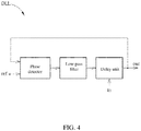
- FIG. 4 is a schematic diagram of a delay lock unit DLL according to an embodiment of the present invention.
- the delay lock loop 348 may be used to implement the delay lock loop 148a.
- the delay lock loop 348 includes a plurality of buffers BFs and a plurality of delay lock units DLLs, where a delay lock unit DLL has input ends in, ref and an output end out, the delay lock unit DLL is configured to lock a delay/phase, so that a signal output by the output end (out) of the delay lock unit DLL and a signal input by the input end (ref) have the same delay/phase, and the detailed circuit structure may refer to FIG. 4 .
- the delay lock loop 348 may ensure that the clock signal CK output by each delay lock unit DLL has the same delay/phase.
- the delay lock loop 348 may also be used to implement the delay lock loop 148b, and the operation principles thereof may refer to the foregoing paragraphs, which will not be repeated redundantly here.
- an image sensor circuit 14 obtains phase differences ⁇ 1 ' ⁇ M ' with a reference pixel array 144, and phase differences ⁇ 1 ⁇ M experienced by photo pixel circuits PX_1 ⁇ PX_M may be compensated by using the phase differences ⁇ 1 ' ⁇ M ' generated by the reference pixel array 144 when an image depth is calculated since the phase differences ⁇ 1 ' ⁇ M ' and the phase differences ⁇ 1 ⁇ M are the same, such that the determination of the image depth is more accurate.
- FIG. 5 is a schematic diagram of an existing pixel array 540.
- received clock signals corresponding to pixel circuits PX_1 ⁇ PX_M have phase differences ⁇ 1 ⁇ M with respect to a clock signal CK without propagation delay; however, in the prior art, compensation is not performed with respect to the phase differences ⁇ 1 ⁇ M , such that the phase differences ⁇ 1 ⁇ M have an influence on calculation of a distance/depth, thereby increasing errors when the distance/depth is calculated.
- a reference pixel array that does not receive illumination (or does not have a photo component) is used to record phase delays/phase differences caused by conduction of a clock signal, and phase differences experienced by a photo pixel array are compensated when an image depth is calculated, so that determination of the image depth is more accurate.
Landscapes
- Engineering & Computer Science (AREA)
- Physics & Mathematics (AREA)
- General Physics & Mathematics (AREA)
- Multimedia (AREA)
- Signal Processing (AREA)
- Radar, Positioning & Navigation (AREA)
- Remote Sensing (AREA)
- Computer Networks & Wireless Communication (AREA)
- Electromagnetism (AREA)
- Theoretical Computer Science (AREA)
- Computer Vision & Pattern Recognition (AREA)
- Measurement Of Optical Distance (AREA)
- Optical Radar Systems And Details Thereof (AREA)
- Transforming Light Signals Into Electric Signals (AREA)
- Length Measuring Devices By Optical Means (AREA)
- Solid State Image Pick-Up Elements (AREA)
Abstract
Description
- The present invention relates to an image sensor circuit and an image depth sensor system, and in particular, to an image sensor circuit and an image depth sensor system which may reduce an influence caused by phase differences of clock signals.
- A 3D image sensor circuit may collect distance/depth information thereof with respect to a target object, and thus three dimensional image data is generated by a value of space or a value of distance between respective pixels of a 3D image, and the 3D image is also referred to as a distance image or a depth image. Additional distance dimension may be used in various applications to obtain more information about an object in a scene captured by a camera, thereby solving different tasks in the field of industrial sensors.
- Generally, in a 3D image sensor circuit, incident light is emitted by a light emitting diode, a plurality of pixel circuits in a pixel array are used to collect reflected light corresponding to the incident light and reflected from a target object, and then a distance/depth between an electronic device (provided with the 3D image sensor circuit) and the target object may be calculated by comparing an optical path difference between the incident light and the reflected light. However, when the pixel array is large, a clock signal input to the pixel array may generate phase differences in the pixel array, causing that errors are generated when in the 3D image sensor circuit calculates the distance/depth between the electronic device and the target object.
- Therefore, it is necessary to improve the prior art.
- Therefore, a main objective of the present invention is to provide an image sensor circuit and an image depth sensor system which may reduce an influence caused by phase differences of clock signals, so as to improve disadvantages of the prior art.
- To solve the foregoing technical problem, the present invention provides an image sensor circuit, including: a photo pixel array, including a plurality of photo pixel series, where a photo pixel series in the plurality of photo pixel series includes a plurality of photo pixel circuits, a first end of the photo pixel series receives a clock signal, the clock signal is propagated (Propagate) from the first end of the photo pixel series to a second end of the photo pixel series, and the photo pixel array outputs a plurality of pixel values; a reference pixel array, including at least one reference pixel series, where a reference pixel series in the at least one reference pixel series includes a plurality of reference pixel circuits, a first end of the reference pixel series receives the clock signal, the clock signal is propagated from the first end of the reference pixel series to a second end of the reference pixel series, and the reference pixel array outputs a plurality of phase differences between a plurality of received clock signals received by the plurality of reference pixel circuits and the clock signal; and an image depth determining unit, coupled to the photo pixel array and the reference pixel array, and configured to determine an image depth according to the plurality of pixel values and the plurality of phase differences.
- Preferably, the plurality of photo pixel series are parallel to each other, and the at least one reference pixel series is parallel to the plurality of photo pixel series.
- Preferably, each photo pixel circuit of the photo pixel array includes a photo component, and each reference pixel circuit of the reference pixel array does not include a photo component.
- Preferably, the reference pixel array does not receive external illumination.
- Preferably, the reference pixel array is disposed adjacent to one side of the photo pixel array.
- The present invention further provides an image depth sensor system, including: a light emitting unit, configured to emit incident light; and an image sensor circuit, including: a photo pixel array, including a plurality of photo pixel series, where a photo pixel series in the plurality of photo pixel series includes a plurality of photo pixel circuits, a first end of the photo pixel series receives a clock signal, the clock signal is propagated from the first end of the photo pixel series to a second end of the photo pixel series, and the photo pixel array outputs a plurality of pixel values; a reference pixel array, including at least one reference pixel series, where a reference pixel series in the at least one reference pixel series includes a plurality of reference pixel circuits, a first end of the reference pixel series receives the clock signal, the clock signal is propagated from the first end of the reference pixel series to a second end of the reference pixel series, and the reference pixel array outputs a plurality of phase differences between a plurality of received clock signals received by the plurality of reference pixel circuits and the clock signal; and an image depth determining unit, coupled to the photo pixel array and the reference pixel array, and configured to determine an image depth according to the plurality of pixel values and the plurality of phase differences.
- According to the present invention, a reference pixel array that does not receive illumination is used to record phase delays/phase differences caused by conduction of a clock signal, and phase differences experienced by a photo pixel array are compensated when an image depth is calculated, so as to solve the disadvantage of an influence of phase differences of clock signals when an image depth is calculated in the prior art.
-
-
FIG. 1 is a schematic diagram of an image depth sensor system according to an embodiment of the present invention. -
FIG. 2 is a schematic diagram of an image sensor circuit according to an embodiment of the present invention. -
FIG. 3 is a schematic diagram of a delay lock loop according to an embodiment of the present invention. -
FIG. 4 is a schematic diagram of a delay lock unit according to an embodiment of the present invention. -
FIG. 5 is a schematic diagram of a pixel array. - To make objectives, technical solutions and advantages of the present invention clearer, a further detailed description on the present invention will be given below in combination with accompanying drawings and embodiments. It should be understood that, specific embodiments described herein are merely used for illustrating the present invention, rather than limiting the present invention.
- In the description and claims, the term "coupled" refers to any direct or indirect electrical connection means, and the term "electrically connected" refers to a direct electrical connection.
- Referring to
FIG. 1, FIG. 1 is a schematic diagram of an imagedepth sensor system 10 according to an embodiment of the present invention. The imagedepth sensor system 10 may be a three dimensional image sensor (Three Dimensional Image Sensor) system, and may sense a distance/depth thereof with respect to a target object (not shown inFIG. 1 ) according to time of flight (Time of Flight, ToF) of ray or light to create a three dimensional image of the target object. The imagedepth sensor system 10 includes alight emitting unit 12 and animage sensor circuit 14, and thelight emitting unit 12 may be a light emitting diode (Light Emitting Diode, LED) with invisible light, such as an infrared light emitting diode. Thelight emitting unit 12 is configured to emit incident light, and theimage sensor circuit 14 may receive reflected light corresponding to the incident light. - Specifically, referring to
FIG. 1 andFIG. 2, FIG. 2 is a schematic diagram of animage sensor circuit 14 according to an embodiment of the present invention. Theimage sensor circuit 14 includes a photo pixel array (Pixel Array) 140, a clocksignal generating circuit 142, areference pixel array 144 and an image depth determining unit 146 (not shown inFIG. 2 ). Theimage sensor circuit 14 receives reflected light corresponding to the incident light using thephoto pixel array 140, and thephoto pixel array 140 outputs a plurality of pixel values. Furthermore, thereference pixel array 144 does not receive external illumination. In an embodiment, an opaque cover plate may be disposed above thereference pixel array 144 such that thereference pixel array 144 does not receive external illumination, and thereference pixel array 144 is configured to record a plurality of phase differences (which will be described hereinafter in detail). The imagedepth determining unit 146 is coupled to thephoto pixel array 140 and thereference pixel array 144, and is configured to receive the plurality of pixel values output by thephoto pixel array 140 and the plurality of phase differences output by thereference pixel array 144, and to determine an image depth according to the plurality of pixel values and the plurality of phase differences. - Specifically, the
photo pixel array 140 includes a plurality of photo pixel series PXSs, a photo pixel series PXS may be a column (Column) or a row (Row) of photo pixels located in thephoto pixel array 140, and the photo pixel series PXS includes a plurality of photo pixel circuits PX_1∼PX_M, where each photo pixel circuit PX_m includes a photo component (where the photo component may be a photo diode (Photo Diode) or a photo transistor (Photo Transistor), and the photo component may be considered as a light-control current source (Light-Control Current Source)). The plurality of photo pixel series PXSs are parallel to each other, where the photo pixel circuit PX_1 is a photo pixel circuit located at a first end (Terminal/End) of the photo pixel series PXS, the photo pixel circuit PX_M is a photo pixel circuit located at a second end of the photo pixel circuit PXS, and the photo pixel circuit PX_1 is the first photo pixel circuit in the photo pixel circuits PX_1∼PX_M that receives a clock signal CK; in other words, the clock signal CK is propagated (Propagate) from the first end of the photo pixel series PXS/ photo pixel circuit PX_1 to the second end of the photo pixel series PXS/ photo pixel circuit PX_M. - Furthermore, the
reference pixel array 144 is disposed adjacent to one side of thephoto pixel array 140, and thereference pixel array 144 includes at least one reference pixel series RPXS, where the reference pixel series RPXS is parallel to the photo pixel series PXS, the reference pixel series RPXS includes a plurality of reference pixel circuits RPX_1∼RPX_M, and each reference pixel circuit RPX_m may not include any photo component. Specifically, the reference pixel circuit RPX_m may have a similar circuit structure with the photo pixel circuit PX_m, and unlike the photo pixel circuit PX_m, the reference pixel circuit RPX_m does not possess the photo component in the photo pixel circuit PX_m, and a voltage-control current source (Voltage-Control Current Source) is used to replace the photo component in the photo pixel circuit PX_m. Similarly, the reference pixel circuit RPX_1 is a reference pixel circuit located at a first end of the reference pixel series RPXS, the reference pixel circuit PX_M is a reference pixel circuit located at a second end of the reference pixel series RPXS, and the reference pixel circuit RPX_1 is the first photo pixel circuit in the reference pixel circuits RPX_1∼RPX_M thatreceives the clock signal CK; in other words, the clock signal CK is propagated from the first end of the reference pixel series PXS/reference pixel circuit RPX_1 to the second end of the reference pixel series PXS/reference pixel circuit RPX_M. - Generally, the clock signal CK is conducted in clock signal transmission lines. In other words, the photo pixel series PXS may include clock signal transmission lines PXTLs, and the clock signal CK is propagated (Propagate) from the first end of the photo pixel series PXS/photo pixel circuit PX_1 to the second end of the photo pixel series PXS/photo pixel circuit PX_M through the clock signal transmission lines PXTLs. Similarly, the reference pixel series RPXS may include clock signal transmission lines' PXTLs', and the clock signal CK is propagated from the first end of the reference pixel series PXS/reference pixel circuit RPX_1 to the second end of the reference pixel series PXS/reference pixel circuit RPX_M through the clock signal transmission lines PXTLs'.
- Clock signals actually received by the photo pixel circuits PX_1∼PX_M of the same photo pixel series PXS (received clock signals for short) have phase differences ϕ1∼ϕM with respect to the clock signal CK without propagation delay (Propagation Delay) since the clock signal CK conducted in the clock signal transmission lines PXTLs has propagation delay, and the phase differences ϕ1∼ϕM may have an influence on calculation of a distance/depth, thereby increasing errors when the distance/depth is calculated.
- Furthermore, received clock signals actually received by the reference pixel circuits RPX_1∼RPX_M of the reference pixel series RPXS have phase differences ϕ1'∼ϕM' with respect to the clock signal CK without propagation delay since the clock signal CK conducted in the clock signal transmission lines PXTLs' also has propagation delay. In an embodiment, the clock signal transmission lines PXTLs and the clock signal transmission lines PXTLs' may be the same transmission media and have the same signal conduction characteristics, and a transmission distance that the clock signal CK reaches the reference pixel circuits RPX_1∼RPX_M is equal to a transmission distance that the clock signal CK reaches the photo pixel circuit PX_1∼PX_M, so that the phase differences ϕ1'∼ϕM' are the same as the phase differences ϕ1∼ϕM.
- In this case, to reduce the influence of the phase differences ϕ1∼ϕM on calculation of the distance/depth, the
image sensor circuit 14 obtains the phase differences ϕ1'∼ϕM' with thereference pixel array 144, and outputs information related to the phase difference ϕ1'∼ϕM' to the imagedepth determining unit 146, and the imagedepth determining unit 146 may compensate the phase differences ϕ1∼ϕM experienced by the photo pixel circuits PX_1∼PX_M according to the phase difference ϕ1'∼ϕM' when the image depth is calculated, such that the determination of the image depth is more accurate. In other words, the imagedepth determining unit 146 may determine the image depth according to the plurality of pixel values output by thephoto pixel array 140 and the phase differences ϕ1'∼ϕM' output by thereference pixel array 144, such that the determination of the image depth is more accurate. - Furthermore, as shown in
FIG. 2 , the photo pixel series PXS is coupled to the clocksignal generating circuit 142 through a delay lock loop (Delay Lock Loop, DLL) 148a, and thedelay lock loop 148a receives a clock signal CK' from the clocksignal generating circuit 142, and generates the clock signal CK according to the clock signal CK'. It should be noted that thedelay lock loop 148a may lock a delay of the clock signal, so that clock signals CKs that are input to each photo pixel series PXS in thephoto pixel array 140 through thedelay lock loop 148a have the same delays/phases. Furthermore, anotherdelay lock loop 148b receives a clock signal CK" from the clocksignal generating circuit 142, generates a reference clock signal RCK according to the clock signal CK", and inputs the reference clock signal RCK to the reference pixel circuits RPX_1∼RPX_M. Similarly, thedelay lock loop 148b may lock a delay of the clock signal, so that reference clock signals RCKs that are input to each reference pixel series RPXS_m through thedelay lock loop 148b have the same delays/phases. - The
delay lock loop 148a and thedelay lock loop 148b may have the same circuit structure, and the circuit structure thereof is well known to those skilled in the art, therefore, a brief description is provided as follows. Referring toFIG. 3 andFIG. 4 ,FIG. 3 is a schematic diagram of adelay lock loop 348 according to an embodiment of the present invention, andFIG. 4 is a schematic diagram of a delay lock unit DLL according to an embodiment of the present invention. Thedelay lock loop 348 may be used to implement thedelay lock loop 148a. Thedelay lock loop 348 includes a plurality of buffers BFs and a plurality of delay lock units DLLs, where a delay lock unit DLL has input ends in, ref and an output end out, the delay lock unit DLL is configured to lock a delay/phase, so that a signal output by the output end (out) of the delay lock unit DLL and a signal input by the input end (ref) have the same delay/phase, and the detailed circuit structure may refer toFIG. 4 . As such, thedelay lock loop 348 may ensure that the clock signal CK output by each delay lock unit DLL has the same delay/phase. In addition, thedelay lock loop 348 may also be used to implement thedelay lock loop 148b, and the operation principles thereof may refer to the foregoing paragraphs, which will not be repeated redundantly here. - It can be seen from the foregoing description that an
image sensor circuit 14 obtains phase differences ϕ1'∼ϕM' with areference pixel array 144, and phase differences ϕ1∼ϕM experienced by photo pixel circuits PX_1∼PX_M may be compensated by using the phase differences ϕ1'∼ϕM' generated by thereference pixel array 144 when an image depth is calculated since the phase differences ϕ1'∼ϕM' and the phase differences ϕ1∼ϕM are the same, such that the determination of the image depth is more accurate. - By comparison, referring to
FIG. 5, FIG. 5 is a schematic diagram of anexisting pixel array 540. In thepixel array 540, received clock signals corresponding to pixel circuits PX_1∼PX_M have phase differences ϕ1∼ϕM with respect to a clock signal CK without propagation delay; however, in the prior art, compensation is not performed with respect to the phase differences ϕ1∼ϕM, such that the phase differences ϕ1∼ϕM have an influence on calculation of a distance/depth, thereby increasing errors when the distance/depth is calculated. - To sum up, according to the present invention, a reference pixel array that does not receive illumination (or does not have a photo component) is used to record phase delays/phase differences caused by conduction of a clock signal, and phase differences experienced by a photo pixel array are compensated when an image depth is calculated, so that determination of the image depth is more accurate.
- The foregoing descriptions are merely preferred embodiments of the present invention, rather than limiting the present invention, and any modifications, equivalent substitutions, improvements and the like, made within the spirit and principle of the present invention, are all encompassed in the protection scope of the present invention.
Claims (10)
- An image sensor circuit, wherein the image sensor circuit comprises:a photo pixel array, comprising a plurality of photo pixel series, wherein a photo pixel series in the plurality of photo pixel series comprises a plurality of photo pixel circuits, a first end of the photo pixel series is configured to receive a clock signal, which is propagated from the first end of the photo pixel series to a second end of the photo pixel series, and the photo pixel array is configured to output a plurality of pixel values;a reference pixel array, comprising at least one reference pixel series, wherein a reference pixel series in the at least one reference pixel series comprises a plurality of reference pixel circuits, a first end of the reference pixel series receives the clock signal, which is propagated from the first end of the reference pixel series to a second end of the reference pixel series, and the reference pixel array outputs a plurality of phase differences between a plurality of received clock signals received by the plurality of reference pixel circuits and the clock signal; andan image depth determining unit, coupled to the photo pixel array and the reference pixel array, and configured to determine an image depth according to the plurality of pixel values and the plurality of phase differences.
- The image sensor circuit according to claim 1, wherein the plurality of photo pixel series are parallel to each other, and the at least one reference pixel series is parallel to the plurality of photo pixel series.
- The image sensor circuit according to claim 1, wherein each photo pixel circuit of the photo pixel array comprises a photo component, and each reference pixel circuit of the reference pixel array does not comprise a photo component.
- The image sensor circuit according to claim 1, wherein the reference pixel array does not receive external illumination.
- The image sensor circuit according to claim 1, wherein the reference pixel array is disposed adjacent to one side of the photo pixel array.
- An image depth sensor system, comprising:a light emitting unit, configured to emit incident light; andan image sensor circuit, comprising:a photo pixel array, comprising a plurality of photo pixel series, wherein a photo pixel series in the plurality of photo pixel series comprises a plurality of photo pixel circuits, a first end of the photo pixel series receives a clock signal, which is propagated from the first end of the photo pixel series to a second end of the photo pixel series, and the photo pixel array outputs a plurality of pixel values;a reference pixel array, comprising at least one reference pixel series, wherein the reference pixel series in the at least one reference pixel series comprises a plurality of reference pixel circuits, a first end of the reference pixel series receives the clock signal, which is propagated from the first end of the reference pixel series to a second end of the reference pixel series, and the reference pixel array outputs a plurality of phase differences between a plurality of received clock signals received by the plurality of reference pixel circuits and the clock signal; andan image depth determining unit, coupled to the photo pixel array and the reference pixel array, and configured to determine an image depth according to the plurality of pixel values and the plurality of phase differences.
- The image depth sensor system according to claim 6, wherein the plurality of photo pixel series are parallel to each other, and the at least one reference pixel series is parallel to the plurality of photo pixel series.
- The image depth sensor system according to claim 6, wherein each photo pixel circuit of the photo pixel array comprises a photo component, and each reference pixel circuit of the reference pixel array does not comprise a photo component.
- The image depth sensor system according to claim 6, wherein the reference pixel array does not receive external illumination.
- The image depth sensor system according to claim 6, wherein the reference pixel array is disposed adjacent to one side of the photo pixel array.
Applications Claiming Priority (1)
| Application Number | Priority Date | Filing Date | Title |
|---|---|---|---|
| PCT/CN2017/097980 WO2019033382A1 (en) | 2017-08-18 | 2017-08-18 | Image sensing circuit and image depth sensing system |
Publications (3)
| Publication Number | Publication Date |
|---|---|
| EP3462730A4 EP3462730A4 (en) | 2019-04-03 |
| EP3462730A1 true EP3462730A1 (en) | 2019-04-03 |
| EP3462730B1 EP3462730B1 (en) | 2020-05-13 |
Family
ID=65361285
Family Applications (1)
| Application Number | Title | Priority Date | Filing Date |
|---|---|---|---|
| EP17804786.6A Active EP3462730B1 (en) | 2017-08-18 | 2017-08-18 | Image sensing circuit and image depth sensing system |
Country Status (5)
| Country | Link |
|---|---|
| US (1) | US10523849B2 (en) |
| EP (1) | EP3462730B1 (en) |
| KR (1) | KR101980722B1 (en) |
| CN (2) | CN109743891B (en) |
| WO (1) | WO2019033382A1 (en) |
Families Citing this family (3)
| Publication number | Priority date | Publication date | Assignee | Title |
|---|---|---|---|---|
| EP3799424B1 (en) | 2019-07-29 | 2023-05-10 | Shenzhen Goodix Technology Co., Ltd. | Three-dimensional image sensor, related three-dimensional image sensing module, and hand-held device |
| WO2022087776A1 (en) * | 2020-10-26 | 2022-05-05 | 深圳市汇顶科技股份有限公司 | Time-of-flight sensor, distance measurement system, and electronic apparatus |
| CN111965660B (en) * | 2020-10-26 | 2021-02-23 | 深圳市汇顶科技股份有限公司 | Time-of-flight sensor, ranging system and electronic device |
Family Cites Families (20)
| Publication number | Priority date | Publication date | Assignee | Title |
|---|---|---|---|---|
| JPH0832877A (en) * | 1994-07-14 | 1996-02-02 | Matsushita Electric Ind Co Ltd | Solid-state imaging device and method for driving solid-state imaging device |
| JP2008032877A (en) | 2006-07-27 | 2008-02-14 | Nikon Corp | Automatic focus detection device |
| JP2010041460A (en) | 2008-08-06 | 2010-02-18 | Renesas Technology Corp | Solid state imaging apparatus |
| JP5335327B2 (en) * | 2008-08-29 | 2013-11-06 | キヤノン株式会社 | Defect detection and correction apparatus and defect detection and correction method |
| KR101646908B1 (en) * | 2009-11-27 | 2016-08-09 | 삼성전자주식회사 | Image sensor for sensing object distance information |
| KR101788032B1 (en) | 2011-03-24 | 2017-10-19 | 삼성전자주식회사 | Depth sensor, depth information error compensation method thereof, and signal processing system having the depth sensor |
| CN103595410A (en) * | 2012-08-17 | 2014-02-19 | 联咏科技股份有限公司 | Image sensor and column analog-to-digital converter thereof |
| JP2014124493A (en) * | 2012-12-27 | 2014-07-07 | Olympus Medical Systems Corp | Endoscope system |
| KR102007279B1 (en) * | 2013-02-08 | 2019-08-05 | 삼성전자주식회사 | Depth pixel included in three-dimensional image sensor, three-dimensional image sensor including the same and method of operating depth pixel included in three-dimensional image sensor |
| US20140347442A1 (en) * | 2013-05-23 | 2014-11-27 | Yibing M. WANG | Rgbz pixel arrays, imaging devices, controllers & methods |
| KR102061699B1 (en) * | 2013-06-19 | 2020-01-02 | 삼성전자주식회사 | An image sensor, image processing system including the same, and an operating method of the same |
| TWI528810B (en) * | 2013-10-07 | 2016-04-01 | 恆景科技股份有限公司 | Image sensor and image sensing method |
| WO2015119243A1 (en) * | 2014-02-07 | 2015-08-13 | 国立大学法人静岡大学 | Image sensor |
| CN104980605B (en) * | 2014-04-11 | 2018-07-03 | 山东新北洋信息技术股份有限公司 | Image-reading device and the phase difference correction method for image-reading device |
| JP6397033B2 (en) | 2014-08-29 | 2018-09-26 | オリンパス株式会社 | Imaging apparatus and imaging system |
| US10061029B2 (en) | 2015-01-06 | 2018-08-28 | Samsung Electronics Co., Ltd. | Correction of depth images from T-O-F 3D camera with electronic-rolling-shutter for light modulation changes taking place during light integration |
| US9819930B2 (en) * | 2015-05-26 | 2017-11-14 | Omnivision Technologies, Inc. | Time of flight imaging with improved initiation signaling |
| CN105609516B (en) * | 2015-12-18 | 2019-04-12 | Oppo广东移动通信有限公司 | Imaging sensor and output method, phase focusing method, imaging device and terminal |
| CN106027881B (en) * | 2016-05-10 | 2019-05-10 | 天津大学 | Image Sensor Column Delay Caused Image Distortion Recovery Method |
| US10527728B2 (en) * | 2017-01-27 | 2020-01-07 | Samsung Electronics Co., Ltd | Apparatus and method for range measurement |
-
2017
- 2017-08-18 CN CN201780000972.2A patent/CN109743891B/en active Active
- 2017-08-18 KR KR1020177033789A patent/KR101980722B1/en active Active
- 2017-08-18 EP EP17804786.6A patent/EP3462730B1/en active Active
- 2017-08-18 WO PCT/CN2017/097980 patent/WO2019033382A1/en not_active Ceased
- 2017-08-18 CN CN202110390402.7A patent/CN113099072B/en active Active
- 2017-11-15 US US15/813,156 patent/US10523849B2/en active Active
Also Published As
| Publication number | Publication date |
|---|---|
| CN109743891A (en) | 2019-05-10 |
| EP3462730B1 (en) | 2020-05-13 |
| KR20190035451A (en) | 2019-04-03 |
| US20190058812A1 (en) | 2019-02-21 |
| US10523849B2 (en) | 2019-12-31 |
| CN109743891B (en) | 2021-06-25 |
| WO2019033382A1 (en) | 2019-02-21 |
| EP3462730A4 (en) | 2019-04-03 |
| KR101980722B1 (en) | 2019-08-28 |
| CN113099072A (en) | 2021-07-09 |
| CN113099072B (en) | 2023-09-26 |
Similar Documents
| Publication | Publication Date | Title |
|---|---|---|
| US11828850B2 (en) | 3D image sensor and related 3D image sensing module and hand-held device | |
| US11604265B2 (en) | Single SPAD array ranging system | |
| JP6286677B2 (en) | Ranging system and imaging sensor | |
| US10523849B2 (en) | Image sensor circuit and image depth sensor system | |
| US11688102B2 (en) | Image capture system with calibration function | |
| EP2717069B1 (en) | Method for determining and/or compensating range offset of a range sensor | |
| KR20160032014A (en) | A method for driving a time-of-flight system | |
| US10033987B2 (en) | Device for generating depth information, method for generating depth information, and stereo camera | |
| US9163959B2 (en) | Position detecting device using reflection type photosensor | |
| US10416294B2 (en) | Ranging device read-out circuit | |
| WO2018211801A1 (en) | Optical sensor and electronic device | |
| US11089245B2 (en) | Image sensor circuit and image depth sensor system | |
| CN111580118A (en) | The launch module of the TOF device of the time of flight | |
| US12374863B2 (en) | Light-emission driving device and light-emitting device | |
| CN213210474U (en) | Time-of-flight TOF apparatus and electronic device | |
| CN213210470U (en) | Emission module of time of flight TOF device | |
| TWI734079B (en) | Image sensing system and multi-function image sensor thereof | |
| US20220208825A1 (en) | High Spatial Resolution Solid-State Image Sensor with Distributed Photomultiplier | |
| KR20220075016A (en) | Imaging device | |
| WO2019196049A1 (en) | Image sensing system and electronic device | |
| JP2023008063A (en) | variable delay circuit | |
| CN113645371A (en) | Time-of-flight sensor row direction phase fixed mode noise canceling device and method |
Legal Events
| Date | Code | Title | Description |
|---|---|---|---|
| STAA | Information on the status of an ep patent application or granted ep patent |
Free format text: STATUS: UNKNOWN |
|
| STAA | Information on the status of an ep patent application or granted ep patent |
Free format text: STATUS: THE INTERNATIONAL PUBLICATION HAS BEEN MADE |
|
| PUAI | Public reference made under article 153(3) epc to a published international application that has entered the european phase |
Free format text: ORIGINAL CODE: 0009012 |
|
| STAA | Information on the status of an ep patent application or granted ep patent |
Free format text: STATUS: REQUEST FOR EXAMINATION WAS MADE |
|
| 17P | Request for examination filed |
Effective date: 20171207 |
|
| A4 | Supplementary search report drawn up and despatched |
Effective date: 20181203 |
|
| AK | Designated contracting states |
Kind code of ref document: A1 Designated state(s): AL AT BE BG CH CY CZ DE DK EE ES FI FR GB GR HR HU IE IS IT LI LT LU LV MC MK MT NL NO PL PT RO RS SE SI SK SM TR |
|
| AX | Request for extension of the european patent |
Extension state: BA ME |
|
| RIN1 | Information on inventor provided before grant (corrected) |
Inventor name: LIANG, YU AN Inventor name: YANG, MENGTA |
|
| STAA | Information on the status of an ep patent application or granted ep patent |
Free format text: STATUS: EXAMINATION IS IN PROGRESS |
|
| 17Q | First examination report despatched |
Effective date: 20190801 |
|
| GRAP | Despatch of communication of intention to grant a patent |
Free format text: ORIGINAL CODE: EPIDOSNIGR1 |
|
| STAA | Information on the status of an ep patent application or granted ep patent |
Free format text: STATUS: GRANT OF PATENT IS INTENDED |
|
| DAV | Request for validation of the european patent (deleted) | ||
| DAX | Request for extension of the european patent (deleted) | ||
| INTG | Intention to grant announced |
Effective date: 20200124 |
|
| GRAS | Grant fee paid |
Free format text: ORIGINAL CODE: EPIDOSNIGR3 |
|
| GRAA | (expected) grant |
Free format text: ORIGINAL CODE: 0009210 |
|
| STAA | Information on the status of an ep patent application or granted ep patent |
Free format text: STATUS: THE PATENT HAS BEEN GRANTED |
|
| AK | Designated contracting states |
Kind code of ref document: B1 Designated state(s): AL AT BE BG CH CY CZ DE DK EE ES FI FR GB GR HR HU IE IS IT LI LT LU LV MC MK MT NL NO PL PT RO RS SE SI SK SM TR |
|
| REG | Reference to a national code |
Ref country code: GB Ref legal event code: FG4D |
|
| REG | Reference to a national code |
Ref country code: CH Ref legal event code: EP |
|
| REG | Reference to a national code |
Ref country code: DE Ref legal event code: R096 Ref document number: 602017016828 Country of ref document: DE |
|
| REG | Reference to a national code |
Ref country code: AT Ref legal event code: REF Ref document number: 1271762 Country of ref document: AT Kind code of ref document: T Effective date: 20200615 |
|
| REG | Reference to a national code |
Ref country code: LT Ref legal event code: MG4D |
|
| REG | Reference to a national code |
Ref country code: NL Ref legal event code: MP Effective date: 20200513 |
|
| PG25 | Lapsed in a contracting state [announced via postgrant information from national office to epo] |
Ref country code: PT Free format text: LAPSE BECAUSE OF FAILURE TO SUBMIT A TRANSLATION OF THE DESCRIPTION OR TO PAY THE FEE WITHIN THE PRESCRIBED TIME-LIMIT Effective date: 20200914 Ref country code: NO Free format text: LAPSE BECAUSE OF FAILURE TO SUBMIT A TRANSLATION OF THE DESCRIPTION OR TO PAY THE FEE WITHIN THE PRESCRIBED TIME-LIMIT Effective date: 20200813 Ref country code: GR Free format text: LAPSE BECAUSE OF FAILURE TO SUBMIT A TRANSLATION OF THE DESCRIPTION OR TO PAY THE FEE WITHIN THE PRESCRIBED TIME-LIMIT Effective date: 20200814 Ref country code: FI Free format text: LAPSE BECAUSE OF FAILURE TO SUBMIT A TRANSLATION OF THE DESCRIPTION OR TO PAY THE FEE WITHIN THE PRESCRIBED TIME-LIMIT Effective date: 20200513 Ref country code: LT Free format text: LAPSE BECAUSE OF FAILURE TO SUBMIT A TRANSLATION OF THE DESCRIPTION OR TO PAY THE FEE WITHIN THE PRESCRIBED TIME-LIMIT Effective date: 20200513 Ref country code: IS Free format text: LAPSE BECAUSE OF FAILURE TO SUBMIT A TRANSLATION OF THE DESCRIPTION OR TO PAY THE FEE WITHIN THE PRESCRIBED TIME-LIMIT Effective date: 20200913 Ref country code: SE Free format text: LAPSE BECAUSE OF FAILURE TO SUBMIT A TRANSLATION OF THE DESCRIPTION OR TO PAY THE FEE WITHIN THE PRESCRIBED TIME-LIMIT Effective date: 20200513 |
|
| PG25 | Lapsed in a contracting state [announced via postgrant information from national office to epo] |
Ref country code: BG Free format text: LAPSE BECAUSE OF FAILURE TO SUBMIT A TRANSLATION OF THE DESCRIPTION OR TO PAY THE FEE WITHIN THE PRESCRIBED TIME-LIMIT Effective date: 20200813 Ref country code: RS Free format text: LAPSE BECAUSE OF FAILURE TO SUBMIT A TRANSLATION OF THE DESCRIPTION OR TO PAY THE FEE WITHIN THE PRESCRIBED TIME-LIMIT Effective date: 20200513 Ref country code: LV Free format text: LAPSE BECAUSE OF FAILURE TO SUBMIT A TRANSLATION OF THE DESCRIPTION OR TO PAY THE FEE WITHIN THE PRESCRIBED TIME-LIMIT Effective date: 20200513 Ref country code: HR Free format text: LAPSE BECAUSE OF FAILURE TO SUBMIT A TRANSLATION OF THE DESCRIPTION OR TO PAY THE FEE WITHIN THE PRESCRIBED TIME-LIMIT Effective date: 20200513 |
|
| REG | Reference to a national code |
Ref country code: AT Ref legal event code: MK05 Ref document number: 1271762 Country of ref document: AT Kind code of ref document: T Effective date: 20200513 |
|
| PG25 | Lapsed in a contracting state [announced via postgrant information from national office to epo] |
Ref country code: NL Free format text: LAPSE BECAUSE OF FAILURE TO SUBMIT A TRANSLATION OF THE DESCRIPTION OR TO PAY THE FEE WITHIN THE PRESCRIBED TIME-LIMIT Effective date: 20200513 Ref country code: AL Free format text: LAPSE BECAUSE OF FAILURE TO SUBMIT A TRANSLATION OF THE DESCRIPTION OR TO PAY THE FEE WITHIN THE PRESCRIBED TIME-LIMIT Effective date: 20200513 |
|
| PG25 | Lapsed in a contracting state [announced via postgrant information from national office to epo] |
Ref country code: AT Free format text: LAPSE BECAUSE OF FAILURE TO SUBMIT A TRANSLATION OF THE DESCRIPTION OR TO PAY THE FEE WITHIN THE PRESCRIBED TIME-LIMIT Effective date: 20200513 Ref country code: IT Free format text: LAPSE BECAUSE OF FAILURE TO SUBMIT A TRANSLATION OF THE DESCRIPTION OR TO PAY THE FEE WITHIN THE PRESCRIBED TIME-LIMIT Effective date: 20200513 Ref country code: RO Free format text: LAPSE BECAUSE OF FAILURE TO SUBMIT A TRANSLATION OF THE DESCRIPTION OR TO PAY THE FEE WITHIN THE PRESCRIBED TIME-LIMIT Effective date: 20200513 Ref country code: DK Free format text: LAPSE BECAUSE OF FAILURE TO SUBMIT A TRANSLATION OF THE DESCRIPTION OR TO PAY THE FEE WITHIN THE PRESCRIBED TIME-LIMIT Effective date: 20200513 Ref country code: SM Free format text: LAPSE BECAUSE OF FAILURE TO SUBMIT A TRANSLATION OF THE DESCRIPTION OR TO PAY THE FEE WITHIN THE PRESCRIBED TIME-LIMIT Effective date: 20200513 Ref country code: EE Free format text: LAPSE BECAUSE OF FAILURE TO SUBMIT A TRANSLATION OF THE DESCRIPTION OR TO PAY THE FEE WITHIN THE PRESCRIBED TIME-LIMIT Effective date: 20200513 Ref country code: ES Free format text: LAPSE BECAUSE OF FAILURE TO SUBMIT A TRANSLATION OF THE DESCRIPTION OR TO PAY THE FEE WITHIN THE PRESCRIBED TIME-LIMIT Effective date: 20200513 Ref country code: CZ Free format text: LAPSE BECAUSE OF FAILURE TO SUBMIT A TRANSLATION OF THE DESCRIPTION OR TO PAY THE FEE WITHIN THE PRESCRIBED TIME-LIMIT Effective date: 20200513 |
|
| REG | Reference to a national code |
Ref country code: DE Ref legal event code: R097 Ref document number: 602017016828 Country of ref document: DE |
|
| PG25 | Lapsed in a contracting state [announced via postgrant information from national office to epo] |
Ref country code: PL Free format text: LAPSE BECAUSE OF FAILURE TO SUBMIT A TRANSLATION OF THE DESCRIPTION OR TO PAY THE FEE WITHIN THE PRESCRIBED TIME-LIMIT Effective date: 20200513 Ref country code: SK Free format text: LAPSE BECAUSE OF FAILURE TO SUBMIT A TRANSLATION OF THE DESCRIPTION OR TO PAY THE FEE WITHIN THE PRESCRIBED TIME-LIMIT Effective date: 20200513 |
|
| PLBE | No opposition filed within time limit |
Free format text: ORIGINAL CODE: 0009261 |
|
| STAA | Information on the status of an ep patent application or granted ep patent |
Free format text: STATUS: NO OPPOSITION FILED WITHIN TIME LIMIT |
|
| PG25 | Lapsed in a contracting state [announced via postgrant information from national office to epo] |
Ref country code: MC Free format text: LAPSE BECAUSE OF FAILURE TO SUBMIT A TRANSLATION OF THE DESCRIPTION OR TO PAY THE FEE WITHIN THE PRESCRIBED TIME-LIMIT Effective date: 20200513 |
|
| REG | Reference to a national code |
Ref country code: CH Ref legal event code: PL |
|
| 26N | No opposition filed |
Effective date: 20210216 |
|
| PG25 | Lapsed in a contracting state [announced via postgrant information from national office to epo] |
Ref country code: CH Free format text: LAPSE BECAUSE OF NON-PAYMENT OF DUE FEES Effective date: 20200831 Ref country code: LU Free format text: LAPSE BECAUSE OF NON-PAYMENT OF DUE FEES Effective date: 20200818 Ref country code: LI Free format text: LAPSE BECAUSE OF NON-PAYMENT OF DUE FEES Effective date: 20200831 |
|
| REG | Reference to a national code |
Ref country code: BE Ref legal event code: MM Effective date: 20200831 |
|
| PG25 | Lapsed in a contracting state [announced via postgrant information from national office to epo] |
Ref country code: SI Free format text: LAPSE BECAUSE OF FAILURE TO SUBMIT A TRANSLATION OF THE DESCRIPTION OR TO PAY THE FEE WITHIN THE PRESCRIBED TIME-LIMIT Effective date: 20200513 |
|
| PG25 | Lapsed in a contracting state [announced via postgrant information from national office to epo] |
Ref country code: FR Free format text: LAPSE BECAUSE OF NON-PAYMENT OF DUE FEES Effective date: 20200831 |
|
| PG25 | Lapsed in a contracting state [announced via postgrant information from national office to epo] |
Ref country code: BE Free format text: LAPSE BECAUSE OF NON-PAYMENT OF DUE FEES Effective date: 20200831 Ref country code: IE Free format text: LAPSE BECAUSE OF NON-PAYMENT OF DUE FEES Effective date: 20200818 |
|
| PG25 | Lapsed in a contracting state [announced via postgrant information from national office to epo] |
Ref country code: TR Free format text: LAPSE BECAUSE OF FAILURE TO SUBMIT A TRANSLATION OF THE DESCRIPTION OR TO PAY THE FEE WITHIN THE PRESCRIBED TIME-LIMIT Effective date: 20200513 Ref country code: MT Free format text: LAPSE BECAUSE OF FAILURE TO SUBMIT A TRANSLATION OF THE DESCRIPTION OR TO PAY THE FEE WITHIN THE PRESCRIBED TIME-LIMIT Effective date: 20200513 Ref country code: CY Free format text: LAPSE BECAUSE OF FAILURE TO SUBMIT A TRANSLATION OF THE DESCRIPTION OR TO PAY THE FEE WITHIN THE PRESCRIBED TIME-LIMIT Effective date: 20200513 |
|
| PG25 | Lapsed in a contracting state [announced via postgrant information from national office to epo] |
Ref country code: MK Free format text: LAPSE BECAUSE OF FAILURE TO SUBMIT A TRANSLATION OF THE DESCRIPTION OR TO PAY THE FEE WITHIN THE PRESCRIBED TIME-LIMIT Effective date: 20200513 |
|
| REG | Reference to a national code |
Ref country code: DE Ref legal event code: R079 Ref document number: 602017016828 Country of ref document: DE Free format text: PREVIOUS MAIN CLASS: H04N0005335000 Ipc: H04N0025000000 |
|
| PGFP | Annual fee paid to national office [announced via postgrant information from national office to epo] |
Ref country code: DE Payment date: 20250805 Year of fee payment: 9 |
|
| PGFP | Annual fee paid to national office [announced via postgrant information from national office to epo] |
Ref country code: GB Payment date: 20250807 Year of fee payment: 9 |