EP3462493A1 - Active matrix substrate, liquid crystal display device, organic electroluminescent display device and method for producing active matrix substrate - Google Patents
Active matrix substrate, liquid crystal display device, organic electroluminescent display device and method for producing active matrix substrate Download PDFInfo
- Publication number
- EP3462493A1 EP3462493A1 EP18196910.6A EP18196910A EP3462493A1 EP 3462493 A1 EP3462493 A1 EP 3462493A1 EP 18196910 A EP18196910 A EP 18196910A EP 3462493 A1 EP3462493 A1 EP 3462493A1
- Authority
- EP
- European Patent Office
- Prior art keywords
- tft
- insulating layer
- semiconductor layer
- active matrix
- matrix substrate
- Prior art date
- Legal status (The legal status is an assumption and is not a legal conclusion. Google has not performed a legal analysis and makes no representation as to the accuracy of the status listed.)
- Withdrawn
Links
Images



Classifications
-
- H—ELECTRICITY
- H10—SEMICONDUCTOR DEVICES; ELECTRIC SOLID-STATE DEVICES NOT OTHERWISE PROVIDED FOR
- H10D—INORGANIC ELECTRIC SEMICONDUCTOR DEVICES
- H10D86/00—Integrated devices formed in or on insulating or conducting substrates, e.g. formed in silicon-on-insulator [SOI] substrates or on stainless steel or glass substrates
- H10D86/01—Manufacture or treatment
- H10D86/021—Manufacture or treatment of multiple TFTs
- H10D86/0221—Manufacture or treatment of multiple TFTs comprising manufacture, treatment or patterning of TFT semiconductor bodies
- H10D86/0223—Manufacture or treatment of multiple TFTs comprising manufacture, treatment or patterning of TFT semiconductor bodies comprising crystallisation of amorphous, microcrystalline or polycrystalline semiconductor materials
- H10D86/0229—Manufacture or treatment of multiple TFTs comprising manufacture, treatment or patterning of TFT semiconductor bodies comprising crystallisation of amorphous, microcrystalline or polycrystalline semiconductor materials characterised by control of the annealing or irradiation parameters
-
- H—ELECTRICITY
- H10—SEMICONDUCTOR DEVICES; ELECTRIC SOLID-STATE DEVICES NOT OTHERWISE PROVIDED FOR
- H10D—INORGANIC ELECTRIC SEMICONDUCTOR DEVICES
- H10D86/00—Integrated devices formed in or on insulating or conducting substrates, e.g. formed in silicon-on-insulator [SOI] substrates or on stainless steel or glass substrates
- H10D86/01—Manufacture or treatment
- H10D86/021—Manufacture or treatment of multiple TFTs
-
- H—ELECTRICITY
- H10—SEMICONDUCTOR DEVICES; ELECTRIC SOLID-STATE DEVICES NOT OTHERWISE PROVIDED FOR
- H10D—INORGANIC ELECTRIC SEMICONDUCTOR DEVICES
- H10D86/00—Integrated devices formed in or on insulating or conducting substrates, e.g. formed in silicon-on-insulator [SOI] substrates or on stainless steel or glass substrates
- H10D86/40—Integrated devices formed in or on insulating or conducting substrates, e.g. formed in silicon-on-insulator [SOI] substrates or on stainless steel or glass substrates characterised by multiple TFTs
-
- H—ELECTRICITY
- H10—SEMICONDUCTOR DEVICES; ELECTRIC SOLID-STATE DEVICES NOT OTHERWISE PROVIDED FOR
- H10D—INORGANIC ELECTRIC SEMICONDUCTOR DEVICES
- H10D86/00—Integrated devices formed in or on insulating or conducting substrates, e.g. formed in silicon-on-insulator [SOI] substrates or on stainless steel or glass substrates
- H10D86/40—Integrated devices formed in or on insulating or conducting substrates, e.g. formed in silicon-on-insulator [SOI] substrates or on stainless steel or glass substrates characterised by multiple TFTs
- H10D86/411—Integrated devices formed in or on insulating or conducting substrates, e.g. formed in silicon-on-insulator [SOI] substrates or on stainless steel or glass substrates characterised by multiple TFTs characterised by materials, geometry or structure of the substrates
-
- H—ELECTRICITY
- H10—SEMICONDUCTOR DEVICES; ELECTRIC SOLID-STATE DEVICES NOT OTHERWISE PROVIDED FOR
- H10D—INORGANIC ELECTRIC SEMICONDUCTOR DEVICES
- H10D86/00—Integrated devices formed in or on insulating or conducting substrates, e.g. formed in silicon-on-insulator [SOI] substrates or on stainless steel or glass substrates
- H10D86/40—Integrated devices formed in or on insulating or conducting substrates, e.g. formed in silicon-on-insulator [SOI] substrates or on stainless steel or glass substrates characterised by multiple TFTs
- H10D86/421—Integrated devices formed in or on insulating or conducting substrates, e.g. formed in silicon-on-insulator [SOI] substrates or on stainless steel or glass substrates characterised by multiple TFTs having a particular composition, shape or crystalline structure of the active layer
- H10D86/423—Integrated devices formed in or on insulating or conducting substrates, e.g. formed in silicon-on-insulator [SOI] substrates or on stainless steel or glass substrates characterised by multiple TFTs having a particular composition, shape or crystalline structure of the active layer comprising semiconductor materials not belonging to the Group IV, e.g. InGaZnO
-
- H—ELECTRICITY
- H10—SEMICONDUCTOR DEVICES; ELECTRIC SOLID-STATE DEVICES NOT OTHERWISE PROVIDED FOR
- H10D—INORGANIC ELECTRIC SEMICONDUCTOR DEVICES
- H10D86/00—Integrated devices formed in or on insulating or conducting substrates, e.g. formed in silicon-on-insulator [SOI] substrates or on stainless steel or glass substrates
- H10D86/40—Integrated devices formed in or on insulating or conducting substrates, e.g. formed in silicon-on-insulator [SOI] substrates or on stainless steel or glass substrates characterised by multiple TFTs
- H10D86/441—Interconnections, e.g. scanning lines
-
- H—ELECTRICITY
- H10—SEMICONDUCTOR DEVICES; ELECTRIC SOLID-STATE DEVICES NOT OTHERWISE PROVIDED FOR
- H10D—INORGANIC ELECTRIC SEMICONDUCTOR DEVICES
- H10D86/00—Integrated devices formed in or on insulating or conducting substrates, e.g. formed in silicon-on-insulator [SOI] substrates or on stainless steel or glass substrates
- H10D86/40—Integrated devices formed in or on insulating or conducting substrates, e.g. formed in silicon-on-insulator [SOI] substrates or on stainless steel or glass substrates characterised by multiple TFTs
- H10D86/451—Integrated devices formed in or on insulating or conducting substrates, e.g. formed in silicon-on-insulator [SOI] substrates or on stainless steel or glass substrates characterised by multiple TFTs characterised by the compositions or shapes of the interlayer dielectrics
-
- H—ELECTRICITY
- H10—SEMICONDUCTOR DEVICES; ELECTRIC SOLID-STATE DEVICES NOT OTHERWISE PROVIDED FOR
- H10D—INORGANIC ELECTRIC SEMICONDUCTOR DEVICES
- H10D86/00—Integrated devices formed in or on insulating or conducting substrates, e.g. formed in silicon-on-insulator [SOI] substrates or on stainless steel or glass substrates
- H10D86/40—Integrated devices formed in or on insulating or conducting substrates, e.g. formed in silicon-on-insulator [SOI] substrates or on stainless steel or glass substrates characterised by multiple TFTs
- H10D86/471—Integrated devices formed in or on insulating or conducting substrates, e.g. formed in silicon-on-insulator [SOI] substrates or on stainless steel or glass substrates characterised by multiple TFTs having different architectures, e.g. having both top-gate and bottom-gate TFTs
-
- H—ELECTRICITY
- H10—SEMICONDUCTOR DEVICES; ELECTRIC SOLID-STATE DEVICES NOT OTHERWISE PROVIDED FOR
- H10D—INORGANIC ELECTRIC SEMICONDUCTOR DEVICES
- H10D86/00—Integrated devices formed in or on insulating or conducting substrates, e.g. formed in silicon-on-insulator [SOI] substrates or on stainless steel or glass substrates
- H10D86/40—Integrated devices formed in or on insulating or conducting substrates, e.g. formed in silicon-on-insulator [SOI] substrates or on stainless steel or glass substrates characterised by multiple TFTs
- H10D86/60—Integrated devices formed in or on insulating or conducting substrates, e.g. formed in silicon-on-insulator [SOI] substrates or on stainless steel or glass substrates characterised by multiple TFTs wherein the TFTs are in active matrices
-
- G—PHYSICS
- G02—OPTICS
- G02F—OPTICAL DEVICES OR ARRANGEMENTS FOR THE CONTROL OF LIGHT BY MODIFICATION OF THE OPTICAL PROPERTIES OF THE MEDIA OF THE ELEMENTS INVOLVED THEREIN; NON-LINEAR OPTICS; FREQUENCY-CHANGING OF LIGHT; OPTICAL LOGIC ELEMENTS; OPTICAL ANALOGUE/DIGITAL CONVERTERS
- G02F1/00—Devices or arrangements for the control of the intensity, colour, phase, polarisation or direction of light arriving from an independent light source, e.g. switching, gating or modulating; Non-linear optics
- G02F1/01—Devices or arrangements for the control of the intensity, colour, phase, polarisation or direction of light arriving from an independent light source, e.g. switching, gating or modulating; Non-linear optics for the control of the intensity, phase, polarisation or colour
- G02F1/13—Devices or arrangements for the control of the intensity, colour, phase, polarisation or direction of light arriving from an independent light source, e.g. switching, gating or modulating; Non-linear optics for the control of the intensity, phase, polarisation or colour based on liquid crystals, e.g. single liquid crystal display cells
- G02F1/133—Constructional arrangements; Operation of liquid crystal cells; Circuit arrangements
- G02F1/136—Liquid crystal cells structurally associated with a semi-conducting layer or substrate, e.g. cells forming part of an integrated circuit
- G02F1/1362—Active matrix addressed cells
- G02F1/1368—Active matrix addressed cells in which the switching element is a three-electrode device
-
- G—PHYSICS
- G02—OPTICS
- G02F—OPTICAL DEVICES OR ARRANGEMENTS FOR THE CONTROL OF LIGHT BY MODIFICATION OF THE OPTICAL PROPERTIES OF THE MEDIA OF THE ELEMENTS INVOLVED THEREIN; NON-LINEAR OPTICS; FREQUENCY-CHANGING OF LIGHT; OPTICAL LOGIC ELEMENTS; OPTICAL ANALOGUE/DIGITAL CONVERTERS
- G02F1/00—Devices or arrangements for the control of the intensity, colour, phase, polarisation or direction of light arriving from an independent light source, e.g. switching, gating or modulating; Non-linear optics
- G02F1/01—Devices or arrangements for the control of the intensity, colour, phase, polarisation or direction of light arriving from an independent light source, e.g. switching, gating or modulating; Non-linear optics for the control of the intensity, phase, polarisation or colour
- G02F1/13—Devices or arrangements for the control of the intensity, colour, phase, polarisation or direction of light arriving from an independent light source, e.g. switching, gating or modulating; Non-linear optics for the control of the intensity, phase, polarisation or colour based on liquid crystals, e.g. single liquid crystal display cells
- G02F1/133—Constructional arrangements; Operation of liquid crystal cells; Circuit arrangements
- G02F1/136—Liquid crystal cells structurally associated with a semi-conducting layer or substrate, e.g. cells forming part of an integrated circuit
- G02F1/1362—Active matrix addressed cells
- G02F1/1368—Active matrix addressed cells in which the switching element is a three-electrode device
- G02F1/13685—Top gates
-
- H—ELECTRICITY
- H10—SEMICONDUCTOR DEVICES; ELECTRIC SOLID-STATE DEVICES NOT OTHERWISE PROVIDED FOR
- H10D—INORGANIC ELECTRIC SEMICONDUCTOR DEVICES
- H10D30/00—Field-effect transistors [FET]
- H10D30/60—Insulated-gate field-effect transistors [IGFET]
- H10D30/67—Thin-film transistors [TFT]
- H10D30/6729—Thin-film transistors [TFT] characterised by the electrodes
- H10D30/673—Thin-film transistors [TFT] characterised by the electrodes characterised by the shapes, relative sizes or dispositions of the gate electrodes
- H10D30/6731—Top-gate only TFTs
-
- H—ELECTRICITY
- H10—SEMICONDUCTOR DEVICES; ELECTRIC SOLID-STATE DEVICES NOT OTHERWISE PROVIDED FOR
- H10D—INORGANIC ELECTRIC SEMICONDUCTOR DEVICES
- H10D30/00—Field-effect transistors [FET]
- H10D30/60—Insulated-gate field-effect transistors [IGFET]
- H10D30/67—Thin-film transistors [TFT]
- H10D30/674—Thin-film transistors [TFT] characterised by the active materials
- H10D30/6741—Group IV materials, e.g. germanium or silicon carbide
- H10D30/6743—Silicon
- H10D30/6745—Polycrystalline or microcrystalline silicon
-
- H—ELECTRICITY
- H10—SEMICONDUCTOR DEVICES; ELECTRIC SOLID-STATE DEVICES NOT OTHERWISE PROVIDED FOR
- H10D—INORGANIC ELECTRIC SEMICONDUCTOR DEVICES
- H10D30/00—Field-effect transistors [FET]
- H10D30/60—Insulated-gate field-effect transistors [IGFET]
- H10D30/67—Thin-film transistors [TFT]
- H10D30/674—Thin-film transistors [TFT] characterised by the active materials
- H10D30/6755—Oxide semiconductors, e.g. zinc oxide, copper aluminium oxide or cadmium stannate
-
- H—ELECTRICITY
- H10—SEMICONDUCTOR DEVICES; ELECTRIC SOLID-STATE DEVICES NOT OTHERWISE PROVIDED FOR
- H10K—ORGANIC ELECTRIC SOLID-STATE DEVICES
- H10K59/00—Integrated devices, or assemblies of multiple devices, comprising at least one organic light-emitting element covered by group H10K50/00
- H10K59/10—OLED displays
- H10K59/12—Active-matrix OLED [AMOLED] displays
Definitions
- Patent Document 1 Japanese Laid-Open Patent Publication No. 2012-134475 discloses an active matrix substrate using an In-Ga-Zn-O-based semiconductor film as the active layer of the TFT.
- a TFT arranged as a switching element for each pixel in the display region is referred to as a "pixel TFT”
- a TFT of a peripheral circuit such as a driver circuit
- circuit TFT With an active matrix substrate using oxide semiconductor TFTs as pixel TFTs, it is preferred to form, as circuit TFTs, oxide semiconductor TFTs using the same oxide semiconductor film as the pixel TFTs, in view of the manufacturing process.
- an oxide semiconductor TFT has a smaller current driving capability than a polycrystalline silicon TFT. Therefore, when a driver monolithic circuit is formed using an oxide semiconductor TFT, the driving capacity may be insufficient. Increasing the size (the channel width) of the TFT in order to compensate for the lack of current driving capability will hinder the attempt to reduce the width of the peripheral region.
- the second gate electrode 23 is provided on the second gate insulating layer 22.
- the second gate electrode 23 opposes the oxide semiconductor layer 21 with the second gate insulating layer 22 interposed therebetween.
- the second gate electrode 23 is formed from the same conductive film as the first gate electrode 13 of the first TFT 10.
- the crystalline silicon semiconductor layer 11 is formed on the first insulating layer IL1. Specifically, first, as shown in FIG. 3D , an amorphous silicon (a-Si) film 11a' is formed on the first insulating layer IL1.
- a-Si amorphous silicon
- a dehydrogenation annealing process for reducing hydrogen in the amorphous silicon film 11a' e.g., an annealing process for 1 to 2 hours at 400°C to 450°C
- the oxide semiconductor layer 21 can be modified.
- the first contact hole CH1, the second contact hole CH2, the third contact hole CH3 and the fourth contact hole CH4 are formed by etching in the interlayer insulating layer 4 and the first gate insulating layer 12. Portions of the crystalline silicon semiconductor layer 11 are exposed through the first contact hole CH1 and the second contact hole CH2, and portions of the oxide semiconductor layer 21 are exposed through the third contact hole CH3 and the fourth contact hole CH4.
- a dielectric layer 6 is provided so as to cover the common electrode 31, and a pixel electrode 30 is provided on the dielectric layer 6.
- the pixel electrode 30 is connected to the drain electrode 25 of the second TFT 20 through a pixel contact hole CHP running through the dielectric layer 6 and the organic insulating layer 5.
- the pixel electrode 30 includes at least one slit.
Landscapes
- Physics & Mathematics (AREA)
- Nonlinear Science (AREA)
- Mathematical Physics (AREA)
- Engineering & Computer Science (AREA)
- Chemical & Material Sciences (AREA)
- Crystallography & Structural Chemistry (AREA)
- Microelectronics & Electronic Packaging (AREA)
- General Physics & Mathematics (AREA)
- Optics & Photonics (AREA)
- Thin Film Transistor (AREA)
- Devices For Indicating Variable Information By Combining Individual Elements (AREA)
- Liquid Crystal (AREA)
- Electroluminescent Light Sources (AREA)
- Recrystallisation Techniques (AREA)
- Metal-Oxide And Bipolar Metal-Oxide Semiconductor Integrated Circuits (AREA)
Abstract
Description
- The present invention relates to an active matrix substrate, and particularly to an active matrix substrate that includes both oxide semiconductor TFTs and crystalline silicon TFTs. The present invention also relates to a liquid crystal display device and an organic electroluminescent display device including such an active matrix substrate, and to a method for producing such an active matrix substrate.
- An active matrix substrate used in a liquid crystal display device, or the like, includes a switching element such as a thin film transistor (hereinafter, "TFT") for each pixel. TFTs using an amorphous silicon film as the active layer (hereinafter, "amorphous silicon TFTs") and TFTs using a polycrystalline silicon film as the active layer (hereinafter, "polycrystalline silicon TFTs") have been widely used as such switching elements.
- In recent years, it has been proposed to use an oxide semiconductor, instead of an amorphous silicon or a polycrystalline silicon, as the material of the active layer of the TFT. A TFT having an oxide semiconductor film as the active layer is referred to as an "oxide semiconductor TFT". Patent Document 1 (Japanese Laid-Open Patent Publication No.
2012-134475 - An oxide semiconductor has a higher mobility than an amorphous silicon. Therefore, an oxide semiconductor TFT is capable of operating faster than an amorphous silicon TFT. Moreover, an oxide semiconductor film is formed by a simpler process than a polycrystalline silicon film, and can therefore be applied to devices that need to have large areas.
- Typically, an active matrix substrate includes a display region and a peripheral region. The display region includes a plurality of pixels (pixel regions) that are arranged in a matrix pattern, and is referred to also as the active region. The peripheral region is located around the display region, and is referred to also as the frame region.
- Provided in the display region are TFTs, one for each pixel, and gate bus lines, source bus lines and pixel electrodes electrically connected respectively to gate electrodes, source electrodes and drain electrodes of the TFTs.
- Driver circuits for driving gate bus lines (scanning lines) and source bus lines (signal lines) are arranged in the peripheral region. Specifically, a gate driver for supplying gate signals (scanning signals) to the gate bus lines and a source driver for supplying source signals (display signals) to the source bus lines are arranged. Driver circuits such as a gate driver and a source driver may be mounted as semiconductor chips (COG (Chip On Glass) mounting), or may be formed monolithically (integrally) on an active matrix substrate. A monolithically-formed driver circuit is referred to as a "driver monolithic circuit". A driver monolithic circuit is normally composed of TFTs.
- Herein, a TFT arranged as a switching element for each pixel in the display region is referred to as a "pixel TFT", and a TFT of a peripheral circuit such as a driver circuit is referred to as a "circuit TFT". With an active matrix substrate using oxide semiconductor TFTs as pixel TFTs, it is preferred to form, as circuit TFTs, oxide semiconductor TFTs using the same oxide semiconductor film as the pixel TFTs, in view of the manufacturing process.
- However, while the mobility of an oxide semiconductor is higher than that of an amorphous silicon as described above, it is lower than that of a polycrystalline silicon by about one order of magnitude. Thus, an oxide semiconductor TFT has a smaller current driving capability than a polycrystalline silicon TFT. Therefore, when a driver monolithic circuit is formed using an oxide semiconductor TFT, the driving capacity may be insufficient. Increasing the size (the channel width) of the TFT in order to compensate for the lack of current driving capability will hinder the attempt to reduce the width of the peripheral region.
- Patent Document 2 (Japanese Laid-Open Patent Publication No.
2010-3910 Patent Document 2, the oxide semiconductor TFT has a bottom gate structure and the polycrystalline silicon TFT has a top gate structure. - However, the configuration of
Patent Document 1 has the following problem. - First, with an oxide semiconductor TFT having a bottom gate structure, the gate insulating layer needs to be relatively thick in order to sufficiently cover the gate electrode, thus lowering the current driving capability. The ON current Ion of a TFT is expressed as shown in Expression (1) below.

- In Expression (1), W is the channel width, L is the channel length, Vg is the gate voltage, and Vth is the threshold voltage. Cox expressed as shown in Expression (2) below. In Expression (2), ε0 is the dielectric constant of vacuum, εr is the relative dielectric constant of the gate insulating layer, and d is the thickness of the gate insulating layer.

- As can be seen from Expressions (1) and (2), the thickness d of the gate insulating layer increases, the ON current Ion decreases.
- With an oxide semiconductor TFT of a bottom gate structure, the source electrode and the drain electrode are designed to overlap with the gate electrode as seen from the substrate normal direction taking into consideration the alignment precision, etc., and the parasitic capacitance is therefore large. Therefore, when used in a large display device with a large number of pixels, the capacitive load will be large, which is disadvantageous for high-speed driving.
- An optimal structure is yet to be found for an active matrix substrate that includes both oxide semiconductor TFTs and crystalline silicon TFTs as described above.
- The present invention has been made in view of this problem, and an object thereof is to realize a suitable structure for an active matrix substrate that includes both oxide semiconductor TFTs and crystalline silicon TFTs.
- An active matrix substrate according to an embodiment of the present invention is an active matrix substrate having a display region defined by a plurality of pixel regions arranged in a matrix pattern, and a peripheral region located around the display region, the active matrix substrate including: a substrate; a first TFT supported on the substrate and including a crystalline silicon semiconductor layer; and a second TFT supported on the substrate and including an oxide semiconductor layer, wherein: each of the first TFT and the second TFT has a top gate structure; and the oxide semiconductor layer is located below the crystalline silicon semiconductor layer.
- In one embodiment, the first TFT includes: the crystalline silicon semiconductor layer; a first gate insulating layer provided on the crystalline silicon semiconductor layer; a first gate electrode provided on the first gate insulating layer and opposing the crystalline silicon semiconductor layer with the first gate insulating layer interposed therebetween; and a first source electrode and a first drain electrode electrically connected to the crystalline silicon semiconductor layer; and the second TFT includes: the oxide semiconductor layer; a second gate insulating layer provided on the oxide semiconductor layer; a second gate electrode provided on the second gate insulating layer and opposing the oxide semiconductor layer with the second gate insulating layer interposed therebetween; and a second source electrode and a second drain electrode electrically connected to the oxide semiconductor layer.
- In one embodiment, the second gate insulating layer of the second TFT includes a lower gate insulating layer, and an upper gate insulating layer located on the lower gate insulating layer.
- In one embodiment, the first gate insulating layer of the first TFT is formed from the same insulating film as the upper gate insulating layer of the second TFT.
- In one embodiment, the crystalline silicon semiconductor layer is provided on an insulating layer that is formed from the same insulating film as the lower gate insulating layer of the second TFT.
- In one embodiment, the first gate electrode of the first TFT and the second gate electrode of the second TFT are formed from the same conductive film.
- In one embodiment, the first TFT is arranged in the peripheral region; and the second TFT is arranged in the display region.
- In one embodiment, the first TFT is arranged in the display region; and the second TFT is arranged in the peripheral region.
- In one embodiment, the oxide semiconductor layer includes an In-Ga-Zn-O-based semiconductor.
- In one embodiment, the In-Ga-Zn-O-based semiconductor includes a crystalline portion.
- A liquid crystal display device according to an embodiment of the present invention includes an active matrix substrate having one of the configurations set forth above.
- An organic electroluminescent display device according to an embodiment of the present invention includes an active matrix substrate having one of the configurations set forth above.
- A method for producing an active matrix substrate according to an embodiment of the present invention is a method for producing an active matrix substrate including a first TFT including a crystalline silicon semiconductor layer and a second TFT including an oxide semiconductor layer, the method including the steps of: (A) forming the oxide semiconductor layer of the second TFT on a substrate; (B) forming a first insulating layer on the substrate and the oxide semiconductor layer; (C) forming the crystalline silicon semiconductor layer of the first TFT on the first insulating layer; (D) forming a second insulating layer on the crystalline silicon semiconductor layer and the first insulating layer; and (E) forming a gate electrode of the first TFT and a gate electrode of the second TFT on the second insulating layer, wherein: the step (C) includes: a step (c-1) of forming an amorphous silicon film on the first insulating layer; and a step (c-2) of performing a laser annealing process on the amorphous silicon film so as to crystallize the amorphous silicon film and modify the oxide semiconductor layer by means of heat that is generated in the laser annealing process.
- In one embodiment, the method for producing an active matrix substrate of the present invention further includes a step (F) of patterning the first insulating layer and the second insulating layer, wherein: the patterning in the step (F) is performed so that a portion of the first insulating layer that overlaps with the oxide semiconductor layer and a portion of the second insulating layer that overlaps with the oxide semiconductor layer become a gate insulating layer of the second TFT, and a portion of the second insulating layer that overlaps with the crystalline silicon semiconductor layer becomes a gate insulating layer of the first TFT.
- In one embodiment, in the step (E), the gate electrode of the first TFT and the gate electrode of the second TFT are formed from the same conductive film.
- In one embodiment, the method for producing an active matrix substrate of the present invention further includes: a step (G) of forming an interlayer insulating film after the step (E); and a step (H) of forming a source electrode and a drain electrode of the first TFT and a source electrode and a drain electrode of the second TFT on the interlayer insulating film.
- In one embodiment, the active matrix substrate has a display region defined by a plurality of pixel regions arranged in a matrix pattern, and a peripheral region located around the display region; the first TFT is arranged in the display region; and the second TFT is arranged in the peripheral region.
- In one embodiment, the active matrix substrate has a display region defined by a plurality of pixel regions arranged in a matrix pattern, and a peripheral region located around the display region; the first TFT is arranged in the peripheral region; and the second TFT is arranged in the display region.
- In one embodiment, the oxide semiconductor layer includes an In-Ga-Zn-O-based semiconductor.
- In one embodiment, the In-Ga-Zn-O-based semiconductor includes a crystalline portion.
- According to an embodiment of the present invention, it is possible to realize a suitable structure for an active matrix substrate that includes both oxide semiconductor TFTs and crystalline silicon TFTs.
-
-
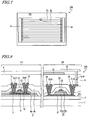
FIG. 1 is a plan view schematically showing anactive matrix substrate 100 according to an embodiment of the present invention. -
FIG. 2 is a cross-sectional view schematically showing theactive matrix substrate 100. -
FIGS. 3A to 3D are cross-sectional views each illustrating a step of a method for producing theactive matrix substrate 100. -
FIGS. 4A to 4D are cross-sectional views each illustrating a step of a method for producing theactive matrix substrate 100. -
FIGS. 5A to 5C are cross-sectional views each illustrating a step of a method for producing theactive matrix substrate 100. -
FIGS. 6A to 6C are cross-sectional views each illustrating a step of a method for producing theactive matrix substrate 100. -
FIG. 7 is a plan view schematically showing anactive matrix substrate 200 according to an embodiment of the present invention. -
FIG. 8 is a cross-sectional view schematically showing theactive matrix substrate 200. -
FIG. 9 is a cross-sectional view schematically showing anactive matrix substrate 300 according to an embodiment of the present invention. -
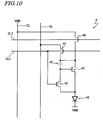
FIG. 10 is a diagram showing an example of an equivalent circuit of one pixel region P of theactive matrix substrate 300. - Embodiments of the present invention will now be described with reference to the drawings. An active matrix substrate according to an embodiment of the present invention can be widely used in various display devices, electronic devices, etc. Note that the present invention is not limited to the embodiments to be described below.
- Referring to
FIG. 1 , anactive matrix substrate 100 of the present embodiment will be described.FIG. 1 is a plan view schematically showing theactive matrix substrate 100. - As shown in
FIG. 1 , theactive matrix substrate 100 includes a display region DR and a peripheral region FR. The display region DR is defined by a plurality of pixel regions P. The pixel regions P are arranged in a matrix pattern including a plurality of rows and a plurality of columns. The display region DR is referred to also as the "active region". The peripheral region FR is located around the display region DR. The peripheral region FR is referred to also as the "frame region". Peripheral circuits (not shown) are provided in the peripheral region FR. - Referring also to
FIG. 2 , a more specific configuration of theactive matrix substrate 100 will be described.FIG. 2 is a cross-sectional view schematically showing theactive matrix substrate 100. - As shown in
FIG. 2 , theactive matrix substrate 100 includes thesubstrate 1, and afirst TFT 10 and asecond TFT 20 supported on thesubstrate 1. - The
first TFT 10 includes a crystallinesilicon semiconductor layer 11 as the active layer. That is, thefirst TFT 10 is a crystalline silicon TFT. In addition to the crystallinesilicon semiconductor layer 11, thefirst TFT 10 includes a firstgate insulating layer 12, afirst gate electrode 13, afirst source electrode 14 and afirst drain electrode 15. - In the present embodiment, the crystalline
silicon semiconductor layer 11 is a polycrystalline silicon layer (e.g., a low-temperature polysilicon (LTPS) layer). In the illustrated example, a base coat layer (base layer) 2 is provided on thesubstrate 1. The crystallinesilicon semiconductor layer 11 is provided on an insulatinglayer 3 formed on thebase coat layer 2. - The first
gate insulating layer 12 is provided on the crystallinesilicon semiconductor layer 11. Thefirst gate electrode 13 is provided on the firstgate insulating layer 12. Thefirst gate electrode 13 opposes the crystallinesilicon semiconductor layer 11 with the firstgate insulating layer 12 interposed therebetween. - The
first source electrode 14 and thefirst drain electrode 15 are electrically connected to the crystallinesilicon semiconductor layer 11. In the present embodiment, aninterlayer insulating layer 4 is provided so as to cover thefirst gate electrode 13, the firstgate insulating layer 12, etc. In the example shown inFIG. 2 , theinterlayer insulating layer 4 includes a lowerinterlayer insulating layer 4a, and an upperinterlayer insulating layer 4b located on the lowerinterlayer insulating layer 4a. That is, theinterlayer insulating layer 4 has a layered structure. Thefirst source electrode 14 and thefirst drain electrode 15 are provided on theinterlayer insulating layer 4. Thefirst source electrode 14 and thefirst drain electrode 15 are connected to the crystallinesilicon semiconductor layer 11 respectively through a first contact hole CH1 and a second contact hole CH2 running through the interlayer insulatinglayer 4 and the firstgate insulating layer 12. - The
second TFT 20 includes anoxide semiconductor layer 21 as the active layer. That is, thesecond TFT 20 is an oxide semiconductor TFT. In addition to theoxide semiconductor layer 21, thesecond TFT 20 includes a secondgate insulating layer 22, asecond gate electrode 23, asecond source electrode 24 and asecond drain electrode 25. - The
oxide semiconductor layer 21 includes an In-Ga-Zn-O-based semiconductor, for example. Theoxide semiconductor layer 21 is provided on thebase coat layer 2. - The second
gate insulating layer 22 is provided on theoxide semiconductor layer 21. The secondgate insulating layer 22 includes a lowergate insulating layer 22a, and an uppergate insulating layer 22b located on the lowergate insulating layer 22a. That is, the secondgate insulating layer 22 has a layered structure. The lowergate insulating layer 22a is formed from the same insulating film as the insulatinglayer 3 located under the crystallinesilicon semiconductor layer 11. The uppergate insulating layer 22b is formed from the same insulating film as the firstgate insulating layer 12 of thefirst TFT 10. - The
second gate electrode 23 is provided on the secondgate insulating layer 22. Thesecond gate electrode 23 opposes theoxide semiconductor layer 21 with the secondgate insulating layer 22 interposed therebetween. Thesecond gate electrode 23 is formed from the same conductive film as thefirst gate electrode 13 of thefirst TFT 10. - The
second source electrode 24 and thesecond drain electrode 25 are electrically connected to theoxide semiconductor layer 21. The interlayer insulatinglayer 4 covers thesecond gate electrode 23, the secondgate insulating layer 22 and theoxide semiconductor layer 21, and thesecond source electrode 24 and thesecond drain electrode 25 are provided on theinterlayer insulating layer 4. Thesecond source electrode 24 and thesecond drain electrode 25 are connected to theoxide semiconductor layer 21 respectively through a third contact hole CH3 and a fourth contact hole CH4 running through the interlayer insulatinglayer 4. As seen from the substrate plane normal direction, thesecond source electrode 24 and thesecond drain electrode 25 do not overlap with thesecond gate electrode 23. - An organic insulating layer (flattening layer) 5 is provided on the
interlayer insulating layer 4 so as to cover thefirst TFT 10 and thesecond TFT 20. - As described above, with the
active matrix substrate 100 of the present embodiment, thefirst TFT 10 and thesecond TFT 20 each have a top gate structure. That is, not only thefirst TFT 10, which is a crystalline silicon TFT, but also thesecond TFT 20, which is an oxide semiconductor TFT, has a top gate structure. - When the
second TFT 20 has a top gate structure, as opposed to a bottom gate structure, the secondgate insulating layer 22 does not need to cover the second gate electrode 23 (i.e., a relatively thick wiring layer), it is possible to reduce the thickness of the secondgate insulating layer 22. Therefore, it is possible to increase the current driving capability of thesecond TFT 20. - Since the
second gate electrode 23 does not need to overlap with thesecond source electrode 24 and thesecond drain electrode 25, it is possible to reduce the parasitic capacitance. Therefore, even when theactive matrix substrate 100 is used in a large display device with a large number of pixels, it is possible to reduce the capacitive load and it is possible to desirably realize high-speed driving. - With the
active matrix substrate 100 of the present embodiment, theoxide semiconductor layer 21 is located below the crystalline silicon semiconductor layer 11 (in other words, the distance from thesubstrate 1 to theoxide semiconductor layer 21 is smaller than the distance from thesubstrate 1 to the crystalline silicon semiconductor layer 11). - With the
oxide semiconductor layer 21 located below the crystallinesilicon semiconductor layer 11, it is possible to modify theoxide semiconductor layer 21 by making use of the laser annealing process that is performed for forming the crystallinesilicon semiconductor layer 11. More specifically, using the heat that is generated in the laser annealing process for crystallizing an amorphous silicon semiconductor film, it is possible to reduce the defect levels of theoxide semiconductor layer 21 to improve the mobility thereof. Moreover, it is also possible to reduce the defect levels of the lowergate insulating layer 22a to improve the reliability. - With the
active matrix substrate 100 of the present embodiment, it is possible to form thefirst gate electrode 13 of thefirst TFT 10 and thesecond gate electrode 23 of thesecond TFT 20 from the same conductive film, thus simplifying the producing process. - Moreover, with the configuration illustrated in
FIG. 2 , the secondgate insulating layer 22 of thesecond TFT 20 includes the lowergate insulating layer 22a in addition to the uppergate insulating layer 22b formed from the same insulating film as the firstgate insulating layer 12 of thefirst TFT 10. Thus, the thickness of the secondgate insulating layer 22 of thesecond TFT 20 is greater than the thickness of the firstgate insulating layer 12 of thefirst TFT 10. Therefore, it is possible to increase the withstand voltage of thesecond TFT 20, thereby allowing thesecond TFT 20 to be driven with a higher voltage than thefirst TFT 10. - Next, an example of a method for producing the
active matrix substrate 100 will be described.FIG. 3A to FIG. 6D are cross-sectional views each illustrating a step of a method for producing theactive matrix substrate 100. - First, as shown in
FIG. 3A , thebase coat layer 2 is formed on thesubstrate 1. Thesubstrate 1 is an insulative transparent substrate (e.g., a glass substrate). Thebase coat layer 2 has a layered structure including a silicon nitride (SiNx) layer as the lower layer and a silicon oxide (SiO2) layer as the upper layer, for example, but it is understood that the structure is not limited to this. - Next, as shown in
FIG. 3B , theoxide semiconductor layer 21 is formed on the substrate 1 (herein, on the base coat layer 2). Specifically, by depositing an oxide semiconductor film on thebase coat layer 2 and then patterning the oxide semiconductor film, it is possible to form theoxide semiconductor layer 21 having an island-like shape. Theoxide semiconductor layer 21 is formed from an In-Ga-Zn-O-based semiconductor whose ratio (composition ratio) between In, Ga and Zn is 1:1:1, for example. The thickness of theoxide semiconductor layer 21 is 10 nm or more and 150 nm or less, for example. - Next, as shown in
FIG. 3C , an insulating layer (hereinafter referred to as the "first insulating layer") IL1 is formed on the substrate 1 (herein, on the base coat layer 2) and on theoxide semiconductor layer 21. The first insulating layer IL1 includes aportion 22a' to be the lowergate insulating layer 22a of thesecond TFT 20, and a portion 3' to be the insulatinglayer 3 that is located under the crystallinesilicon semiconductor layer 11 of thefirst TFT 10. The first insulating layer IL1 is a silicon oxide (SiO2) layer having a thickness of 30 nm or more and 70 nm or less, for example. - Next, the crystalline
silicon semiconductor layer 11 is formed on the first insulating layer IL1. Specifically, first, as shown inFIG. 3D , an amorphous silicon (a-Si)film 11a' is formed on the first insulating layer IL1. - Next, as shown in
FIG. 4A , a laser annealing process is performed by irradiating theamorphous silicon film 11a' with excimer laser light. Thus, theamorphous silicon film 11a' is crystallized to be a crystalline silicon film 11'. At this point, theoxide semiconductor layer 21 is modified by the heat that is generated in the laser annealing process. The light energy of the laser annealing process is absorbed by theamorphous silicon film 11a' and converted to heat, thereby melting and crystallizing the amorphous silicon. The heat in this process is transmitted also to theoxide semiconductor layer 21 via the first insulating layer IL1 (theportion 22a' to be the lowergate insulating layer 22a) (thermal annealing effect), thereby reducing the defect levels of theoxide semiconductor layer 21 and improving the mobility thereof. This also reduces the defect levels of theportion 22a' to be the lowergate insulating layer 22a, improving the reliability. Moreover, since the laser annealing process is performed with the first insulating layer IL1 and theamorphous silicon film 11a' layered on theoxide semiconductor layer 21, the composition does not change due to a metal component whose vapor pressure is low and oxygen being discharged to the outside from theoxide semiconductor layer 21, thus realizing a desirable annealing effect. There is no particular restriction on the conditions of the laser annealing process, and it is possible to use any of various conditions known in the art for crystallizing an amorphous silicon film to obtain a crystalline silicon film. - Typically, a dehydrogenation annealing process for reducing hydrogen in the
amorphous silicon film 11a' (e.g., an annealing process for 1 to 2 hours at 400°C to 450°C) is performed after the formation of theamorphous silicon film 11a' and before the laser annealing process. Also during this dehydrogenation annealing process, theoxide semiconductor layer 21 can be modified. - Next, as shown in
FIG. 4B , the crystalline silicon film 11' is patterned, thereby forming the crystallinesilicon semiconductor layer 11 having an island-like shape. The thickness of the crystallinesilicon semiconductor layer 11 is 30 nm or more and 100 nm or less, for example. - Next, as shown in
FIG. 4C , an insulating layer (hereinafter referred to as a "second insulating layer") IL2 is formed on the crystallinesilicon semiconductor layer 11 and the first insulating layer IL1. The second insulating layer IL2 includes a portion 12' to be the firstgate insulating layer 12 of thefirst TFT 10, and aportion 22b' to be the uppergate insulating layer 22b of thesecond TFT 20. The second insulating layer IL2 is a silicon oxide (SiO2) layer having a thickness of 70 nm or more and 120 nm or less, for example. - Next, the
first gate electrode 13 and thesecond gate electrode 23 are formed on the second insulating layer IL2. Specifically, first, as shown inFIG. 4D , a gate conductive film (gate metal film) GM is formed on the second insulating layer IL2. The material of the gate conductive film GM may be a metal such as molybdenum (Mo), tungsten (W), aluminum (Al), copper (Cu), titanium (Ti), tantalum (Ta), etc., or an alloy thereof, for example. The gate conductive film GM may have a layered structure including a plurality of layers formed from different conducive materials. The thickness of the gate conductive film GM is 50 nm or more and 500 nm or less, for example. - Next, as shown in
FIGS. 5A and 5B , the gate conductive film GM is patterned by etching so as to form thefirst gate electrode 13 and thesecond gate electrode 23. In this process, as shown inFIG. 5A , the first insulating layer IL1 and the second insulating layer IL2 are also patterned by etching so that a portion of the first insulating layer IL1 that overlaps with theoxide semiconductor layer 21 and a portion of the second insulating layer IL2 that overlaps with the oxide semiconductor layer become the secondgate insulating layer 22, and a portion of the second insulating layer IL2 that overlaps with the crystallinesilicon semiconductor layer 11 becomes the firstgate insulating layer 12. - Next, the crystalline
silicon semiconductor layer 11 is doped with an impurity using thefirst gate electrode 13 as a mask, thereby forming the source region and the drain region. A region of the crystallinesilicon semiconductor layer 11 that is not doped with an impurity becomes the channel region (active region). - Next, as shown in
FIG. 5C , theinterlayer insulating layer 4 is formed so as to cover thefirst gate electrode 13, thesecond gate electrode 23, the firstgate insulating layer 12, the secondgate insulating layer 22 and theoxide semiconductor layer 21. The lowerinterlayer insulating layer 4a is a silicon nitride (SiNx) layer, for example, and the upperinterlayer insulating layer 4b is a silicon oxide (SiO2) layer, for example. - Next, as shown in
FIG. 6A , the first contact hole CH1, the second contact hole CH2, the third contact hole CH3 and the fourth contact hole CH4 are formed by etching in theinterlayer insulating layer 4 and the firstgate insulating layer 12. Portions of the crystallinesilicon semiconductor layer 11 are exposed through the first contact hole CH1 and the second contact hole CH2, and portions of theoxide semiconductor layer 21 are exposed through the third contact hole CH3 and the fourth contact hole CH4. - Next, as shown in
FIG. 6B , thefirst source electrode 14, thefirst drain electrode 15, thesecond source electrode 24 and thesecond drain electrode 25 are formed on theinterlayer insulating layer 4. Specifically, a source-drain conductive film (source metal film) is formed on theinterlayer insulating layer 4 and then the source-drain conductive film is patterned, thereby forming thefirst source electrode 14, thefirst drain electrode 15, thesecond source electrode 24 and thesecond drain electrode 25. The material of the source-drain conductive film may be a metal such as molybdenum (Mo), tungsten (W), aluminum (Al), copper (Cu), titanium (Ti), tantalum (Ta), etc., or an alloy thereof, for example. The thickness of the source-drain conductive film is 100 nm or more and 500 nm or less, for example. - Then, as shown in
FIG. 6C , the organic insulatinglayer 5 is formed that covers thefirst TFT 10 and thesecond TFT 20. The organic insulatinglayer 5 is formed from a photosensitive resin material, for example. The thickness of the organic insulatinglayer 5 is 1.5 µm or more and 3.0 µm or less, for example. - Thus, the
active matrix substrate 100 can be obtained. - Note that a metal layer that overlaps with the crystalline
silicon semiconductor layer 11 and a metal layer that overlaps with theoxide semiconductor layer 21 may be provided between thesubstrate 1 and thebase coat layer 2. A metal layer that overlaps with the crystallinesilicon semiconductor layer 11 functions as a light-blocking layer. A metal layer that overlaps with theoxide semiconductor layer 21 may function as an additional gate electrode (back gate electrode) by being given a predetermined potential, thereby further improving the current driving capability of thesecond TFT 20. - Referring to
FIG. 7 and FIG. 8 , anactive matrix substrate 200 of the present embodiment will be described.FIG. 7 and FIG. 8 are a plan view and a cross-sectional view, respectively, schematically showing theactive matrix substrate 200. The description below will focus on differences between theactive matrix substrate 200 and theactive matrix substrate 100 ofEmbodiment 1. - The
active matrix substrate 200 of the present embodiment is used in a liquid crystal display device of the FFS (Fringe Field Switching) mode. Peripheral circuits are provided in the peripheral region FR of theactive matrix substrate 200.FIG. 7 illustrates agate driver circuit 61 as a peripheral circuit. Thegate driver circuit 61 supplies a scanning signal to a plurality of gate bus lines GL. - In the present embodiment, as shown in
FIG. 8 , thefirst TFT 10 is arranged in the peripheral region FR, and is a circuit TFT of a peripheral circuit (e.g., the gate driver circuit 61). In contrast, thesecond TFT 20 is arranged in the display region DR, and is a pixel TFT that is arranged for each of the pixel regions. - In the example shown in
FIG. 8 , acommon electrode 31 is provided on the organic insulatinglayer 5. Thecommon electrode 31 is provided commonly for a plurality of pixel regions P, thereby giving a common potential across the entire display region DR. - A
dielectric layer 6 is provided so as to cover thecommon electrode 31, and apixel electrode 30 is provided on thedielectric layer 6. Thepixel electrode 30 is connected to thedrain electrode 25 of thesecond TFT 20 through a pixel contact hole CHP running through thedielectric layer 6 and the organic insulatinglayer 5. Although not shown in the figures, thepixel electrode 30 includes at least one slit. - As described above, with the
active matrix substrate 200 of the present embodiment, thefirst TFT 10, which is a crystalline silicon TFT, is arranged in the peripheral region FR, and thesecond TFT 20, which is an oxide semiconductor TFT, is arranged in the display region DR. Thus, as thefirst TFT 10, which is a crystalline silicon TFT having a large current driving capability (a high mobility), is used as a circuit TFT, it is possible to reduce the peripheral region (frame region) FR. As thesecond TFT 20, which is an oxide semiconductor TFT having a desirable off-leak characteristic, is used as a pixel TFT, it is possible to realize low-frequency driving and to significantly reduce the power consumption. - Referring to
FIG. 9 , anactive matrix substrate 300 of the present embodiment will be described.FIG. 9 is a cross-sectional view schematically showing theactive matrix substrate 300. - The
active matrix substrate 300 of the present embodiment is used in a bottom emission-type organic EL (electroluminescence) display device. - In the present embodiment, as shown in
FIG. 9 , thefirst TFT 10 is a pixel TFT arranged in the display region DR. In contrast, thesecond TFT 20 is a circuit TFT arranged in the peripheral region FR. - With the
active matrix substrate 300, an inorganic insulating layer (protection layer) 7 is provided on theinterlayer insulating layer 4 so as to cover thefirst source electrode 14, etc., and a color filter layer 8 is provided on the inorganic insulatinglayer 7. Then, theflattening layer 5 is provided on the color filter layer 8, and thepixel electrode 30 is provided on theflattening layer 5. Thepixel electrode 30 is connected to thedrain electrode 15 of thefirst TFT 10 through the pixel contact hole CHP running through theflattening layer 5, the color filter layer 8 and the inorganic insulatinglayer 7. - As described above, with .the
active matrix substrate 300 of the present embodiment, thefirst TFT 10, which is a crystalline silicon TFT, is arranged in the display region DR, and thesecond TFT 20, which is an oxide semiconductor TFT, is arranged in the peripheral region FR. In order to desirably produce multi-gray level display on an organic EL display device, it is preferred that the Vg (gate voltage) - Id (drain current) characteristic of the pixel TFT is somewhat gentle (i.e., not steep), but it may be difficult, with oxide semiconductor TFTs that have currently been in practical use, to realize such a Vg-Id characteristic. By arranging thefirst TFT 10 in the display region DR and arranging thesecond TFT 20 in the peripheral region FR as in the present embodiment, it is possible to desirably produce multi-gray level display. - With the
active matrix substrate 300 for an organic EL display device, two or more TFTs may be arranged in each pixel region P.FIG. 10 shows an example of an equivalent circuit of one pixel region P of theactive matrix substrate 300. - In the example shown in
FIG. 10 , the pixel region P includes adriver TFT 41, aselection TFT 42, a firstcurrent switching TFT 43, a second current switchingTFT 44, acapacitor 45 and an OLED (organic light-emitting diode) 46. - The gate electrode of the
driver TFT 41 is connected to the source electrode of theselection TFT 42, and one of a pair of electrodes (the first electrode) of thecapacitor 45. The source electrode of thedriver TFT 41 is connected to the drain electrodes of the first and second current switchingTFTs driver TFT 41 is connected to the drain electrode of theselection TFT 42 and the anode electrode of theOLED 46. - The gate electrode of the
selection TFT 42 is connected to a first gate bus line GL1. The source electrode of theselection TFT 42 is connected to the gate electrode of thedriver TFT 41. The drain electrode of theselection TFT 42 is connected to the drain electrode of thedriver TFT 41. - The gate electrode of the first
current switching TFT 43 is connected to the first gate bus line GL1. The source electrode of the firstcurrent switching TFT 43 is connected to a source bus line SL. The drain electrode of the firstcurrent switching TFT 43 is connected to the source electrode of thedriver TFT 41 and the other one of the pair of electrodes (second electrode) of thecapacitor 45. - The gate electrode of the second current switching
TFT 44 is connected to a second gate bus line GL2. The source electrode of the second current switchingTFT 44 is connected to the current supply line CL. The current supply line CL is connected to the positive power supply VDD. The drain electrode of the second current switchingTFT 44 is connected to the source electrode of thedriver TFT 41. - The
OLED 46 includes an anode electrode connected to the drain electrode of thedriver TFT 41, an organic EL layer formed on the anode electrode, and a cathode electrode formed on the organic EL layer. For example, the organic EL layer has a layered structure of hole transporting layer / organic light-emitting layer / electron transporting layer, or a layered structure of hole injection layer / hole transporting layer / organic light-emitting layer / electron transporting layer / electron injection layer. The organic EL layer may further include a layer for improving the emission efficiency or the lifetime of the organic light-emitting layer. The cathode electrode is connected to the negative power supply VSS. - The pixel circuit shown in
FIG. 10 operates as follows. - First, when the
selection TFT 42 and the firstcurrent switching TFT 43 are selected by the first gate bus line GL1 to achieve an ON state, thedriver TFT 41 is brought into a state where the gate electrode thereof and the drain electrode thereof are connected together, i.e., in a diode-connected state. Thus, thecapacitor 45 is charged with a voltage that corresponds to the data current IDATA supplied from the source bus line SL. - Next, when the
selection TFT 42 and the firstcurrent switching TFT 43 are OFF, and the second current switchingTFT 44 is selected by the second gate bus line GL2 to achieve an ON state, the current from the current supply line CL is supplied to theOLED 46 via the second current switchingTFT 44 and the driver TFT 41 (being ON with the voltage charged in the capacitor 45), thereby lighting theOLED 46. - The
driver TFT 41 in the configuration illustrated inFIG. 10 corresponds to thefirst TFT 10 shown inFIG. 9 . That is, thedriver TFT 41 is a crystalline silicon TFT. Theselection TFT 42, the firstcurrent switching TFT 43 and the second current switchingTFT 44 may be crystalline silicon TFTs or oxide semiconductor TFTs. - The oxide semiconductor included in the
oxide semiconductor layer 21 may be an amorphous oxide semiconductor or a crystalline oxide semiconductor including a crystalline portion. The crystalline oxide semiconductor may be a polycrystalline oxide semiconductor, a microcrystalline oxide semiconductor, a crystalline oxide semiconductor in which the c axis is oriented generally perpendicular to the layer plane, etc. - The
oxide semiconductor layer 21 may have a layered structure of two or more layers. When theoxide semiconductor layer 21 has a layered structure, theoxide semiconductor layer 21 may include an amorphous oxide semiconductor layer and a crystalline oxide semiconductor layer, may include a plurality of crystalline oxide semiconductor layers of different crystalline structures, or may include a plurality of amorphous oxide semiconductor layers. When theoxide semiconductor layer 21 has a two-layer structure including an upper layer and a lower layer, the energy gap of the oxide semiconductor included in the upper layer is preferably smaller than the energy gap of the oxide semiconductor included in the lower layer. Note however that when the difference between the energy gaps of these layers is relatively small, the energy gap of the oxide semiconductor of the lower layer may be smaller than the energy gap of the oxide semiconductor of the upper layer. - Materials, structures and deposition methods of the amorphous oxide semiconductor and the crystalline oxide semiconductors described above, and the configuration of the oxide semiconductor layer having a layered structure, etc., are described in Japanese Laid-Open Patent Publication No.
2014-007399 2014-007399 - The
oxide semiconductor layer 21 may include at least one metal element from among In, Ga and Zn, for example. In an embodiment of the present invention, theoxide semiconductor layer 21 includes an In-Ga-Zn-O-based semiconductor (e.g., indium gallium zinc oxide), for example. Herein, an In-Ga-Zn-O-based semiconductor is a ternary oxide of In (indium), Ga (gallium) and Zn (zinc), and the ratio (composition ratio) between In, Ga and Zn is not limited to any particular ratio and may be In:Ga:Zn=2:2:1, In:Ga:Zn=1:1:1, In:Ga:Zn=1:1:2, or the like, for example. Such anoxide semiconductor layer 21 can be formed from an oxide semiconductor film including an In-Ga-Zn-O-based semiconductor. - An In-Ga-Zn-O-based semiconductor may be amorphous or crystalline. A crystalline In-Ga-Zn-O-based semiconductor is preferably a crystalline In-Ga-Zn-O-based semiconductor whose c axis is oriented generally perpendicular to the layer plane.
- Note that The crystalline structure of the crystalline In-Ga-Zn-O-based semiconductor is disclosed in Japanese Laid-Open Patent Publication No.
2014-007399 2012-134475 2014-209727 2012-134475 2014-209727 - The
oxide semiconductor layer 21 may include another oxide semiconductor instead of an In-Ga-Zn-O-based semiconductor. For example, it may include an In-Sn-Zn-O-based semiconductor (e.g., In2O3-SnO2-ZnO; InSnZnO). An In-Sn-Zn-O-based semiconductor is a ternary oxide of In (indium), Sn (tin) and Zn (zinc). Alternatively, theoxide semiconductor layer 21 may include an In-Al-Zn-O-based semiconductor, an In-Al-Sn-Zn-O-based semiconductor, a Zn-O-based semiconductor, an In-Zn-O-based semiconductor, a Zn-Ti-O-based semiconductor, a Cd-Ge-O-based semiconductor, a Cd-Pb-O-based semiconductor, a CdO (cadmium oxide), an Mg-Zn-O-based semiconductor, an In-Ga-Sn-O-based semiconductor, an In-Ga-O-based semiconductor, a Zr-In-Zn-O-based semiconductor, an Hf-In-Zn-O-based semiconductor, etc. - An active matrix substrate according to an embodiment of the present invention can desirably be used in a display device, e.g., an liquid crystal display device and an organic EL display device. A liquid crystal display device includes an active matrix substrate according to an embodiment of the present invention, a counter substrate arranged so as to oppose the active matrix substrate, and a liquid crystal layer provided between the active matrix substrate and the counter substrate. Note that although an active matrix substrate for a liquid crystal display device of the FFS mode has been described above, an active matrix substrate according to an embodiment of the present invention can be used in liquid crystal display devices of various display modes. An active matrix substrate according to an embodiment of the present invention can also be used in a liquid crystal display device of a transverse electric field mode other than the FFS mode (e.g., the IPS mode), and in a liquid crystal display device of a vertical electric field mode (e.g., the TN mode or the vertical alignment mode). An organic EL display device may include an active matrix substrate according to an embodiment of the present invention, an organic layer provided on the pixel electrode, and a common electrode provided on the organic layer.
- According to an embodiment of the present invention, it is possible to realize a suitable structure for an active matrix substrate that includes both oxide semiconductor TFTs and crystalline silicon TFTs. An active matrix substrate according to an embodiment of the present invention can be desirably used in a display device such as a liquid crystal display device or an organic electroluminescent display device.
- This application is based on Japanese Patent Applications No.
2017-187574 filed on September 28, 2017
Claims (15)
- An active matrix substrate having a display region defined by a plurality of pixel regions arranged in a matrix pattern, and a peripheral region located around the display region, the active matrix substrate comprising:a substrate;a first TFT supported on the substrate and including a crystalline silicon semiconductor layer; anda second TFT supported on the substrate and including an oxide semiconductor layer, wherein:each of the first TFT and the second TFT has a top gate structure; andthe oxide semiconductor layer is located below the crystalline silicon semiconductor layer.
- The active matrix substrate according to claim 1, wherein:the first TFT includes:the crystalline silicon semiconductor layer;a first gate insulating layer provided on the crystalline silicon semiconductor layer;a first gate electrode provided on the first gate insulating layer and opposing the crystalline silicon semiconductor layer with the first gate insulating layer interposed therebetween; anda first source electrode and a first drain electrode electrically connected to the crystalline silicon semiconductor layer; andthe second TFT includes:the oxide semiconductor layer;a second gate insulating layer provided on the oxide semiconductor layer;a second gate electrode provided on the second gate insulating layer and opposing the oxide semiconductor layer with the second gate insulating layer interposed therebetween; anda second source electrode and a second drain electrode electrically connected to the oxide semiconductor layer.
- The active matrix substrate according to claim 2, wherein the second gate insulating layer of the second TFT includes a lower gate insulating layer, and an upper gate insulating layer located on the lower gate insulating layer.
- The active matrix substrate according to claim 3, wherein the first gate insulating layer of the first TFT is formed from the same insulating film as the upper gate insulating layer of the second TFT.
- The active matrix substrate according to claim 3 or 4, wherein the crystalline silicon semiconductor layer is provided on an insulating layer that is formed from the same insulating film as the lower gate insulating layer of the second TFT.
- The active matrix substrate according to any one of claims 2 to 5, wherein the first gate electrode of the first TFT and the second gate electrode of the second TFT are formed from the same conductive film.
- The active matrix substrate according to any one of claims 1 to 6, wherein, wherein:the first TFT is arranged in the peripheral region; andthe second TFT is arranged in the display region.
- The active matrix substrate according to any one of claims 1 to 6, wherein:the first TFT is arranged in the display region; andthe second TFT is arranged in the peripheral region.
- The active matrix substrate according to any one of claims 1 to 8, wherein the oxide semiconductor layer includes an In-Ga-Zn-O-based semiconductor.
- The active matrix substrate according to claim 9, wherein the In-Ga-Zn-O-based semiconductor includes a crystalline portion.
- A liquid crystal display device comprising the active matrix substrate according to any one of claims 1 to 10.
- An organic electroluminescent display device comprising the active matrix substrate according to any one of claims 1 to 10.
- A method for producing an active matrix substrate comprising a first TFT including a crystalline silicon semiconductor layer and a second TFT including an oxide semiconductor layer, the method comprising the steps of:(A) forming the oxide semiconductor layer of the second TFT on a substrate;(B) forming a first insulating layer on the substrate and the oxide semiconductor layer;(C) forming the crystalline silicon semiconductor layer of the first TFT on the first insulating layer;(D) forming a second insulating layer on the crystalline silicon semiconductor layer and the first insulating layer; and(E) forming a gate electrode of the first TFT and a gate electrode of the second TFT on the second insulating layer, wherein:the step (C) includes:a step (c-1) of forming an amorphous silicon film on the first insulating layer; anda step (c-2) of performing a laser annealing process on the amorphous silicon film so as to crystallize the amorphous silicon film and modify the oxide semiconductor layer by means of heat that is generated in the laser annealing process.
- The method for producing an active matrix substrate according to claim 13, further comprising a step (F) of patterning the first insulating layer and the second insulating layer, wherein:the patterning in the step (F) is performed so that a portion of the first insulating layer that overlaps with the oxide semiconductor layer and a portion of the second insulating layer that overlaps with the oxide semiconductor layer become a gate insulating layer of the second TFT, and a portion of the second insulating layer that overlaps with the crystalline silicon semiconductor layer becomes a gate insulating layer of the first TFT.
- The method for producing an active matrix substrate according to claim 13 or 14, wherein in the step (E), the gate electrode of the first TFT and the gate electrode of the second TFT are formed from the same conductive film.
Applications Claiming Priority (1)
| Application Number | Priority Date | Filing Date | Title |
|---|---|---|---|
| JP2017187574A JP6684769B2 (en) | 2017-09-28 | 2017-09-28 | Active matrix substrate, liquid crystal display device, organic EL display device, and method of manufacturing active matrix substrate |
Publications (1)
| Publication Number | Publication Date |
|---|---|
| EP3462493A1 true EP3462493A1 (en) | 2019-04-03 |
Family
ID=64270578
Family Applications (1)
| Application Number | Title | Priority Date | Filing Date |
|---|---|---|---|
| EP18196910.6A Withdrawn EP3462493A1 (en) | 2017-09-28 | 2018-09-26 | Active matrix substrate, liquid crystal display device, organic electroluminescent display device and method for producing active matrix substrate |
Country Status (4)
| Country | Link |
|---|---|
| US (1) | US10937813B2 (en) |
| EP (1) | EP3462493A1 (en) |
| JP (1) | JP6684769B2 (en) |
| CN (1) | CN109585456B (en) |
Families Citing this family (15)
| Publication number | Priority date | Publication date | Assignee | Title |
|---|---|---|---|---|
| KR102448325B1 (en) | 2017-11-16 | 2022-09-30 | 삼성디스플레이 주식회사 | Display panel and electronic device including same |
| US10991576B2 (en) * | 2018-10-31 | 2021-04-27 | Taiwan Semiconductor Manufacturing Co., Ltd. | Crystalline semiconductor layer formed in BEOL processes |
| CN110137182A (en) * | 2019-04-04 | 2019-08-16 | 惠科股份有限公司 | Array substrate, manufacturing method thereof and display panel |
| KR20210004795A (en) | 2019-07-04 | 2021-01-13 | 엘지디스플레이 주식회사 | Display apparatus having an oxide semiconductor pattern |
| CN112186004A (en) | 2019-07-04 | 2021-01-05 | 乐金显示有限公司 | Display device |
| CN110649044B (en) * | 2019-09-30 | 2022-02-25 | 厦门天马微电子有限公司 | Array substrate, manufacturing method thereof, display panel and display device |
| KR102635368B1 (en) * | 2019-12-16 | 2024-02-08 | 엘지디스플레이 주식회사 | Thin film transistor array substrate and electronic device including the same |
| US11631704B2 (en) * | 2020-04-21 | 2023-04-18 | Sharp Kabushiki Kaisha | Active matrix substrate and display device |
| JP2022014108A (en) * | 2020-07-06 | 2022-01-19 | シャープ株式会社 | Active matrix substrate and manufacturing method for the same |
| JP2022014107A (en) * | 2020-07-06 | 2022-01-19 | シャープ株式会社 | Active matrix substrate and manufacturing method for the same |
| US12550379B2 (en) | 2021-09-03 | 2026-02-10 | Lg Display Co., Ltd. | Thin film transistor substrate and display device comprising the same |
| US12363952B2 (en) * | 2021-12-09 | 2025-07-15 | AUP Corporation | Active device substrate and manufacturing method of active device substrate |
| EP4365955B1 (en) * | 2022-11-07 | 2025-03-12 | Imec VZW | A method for forming a semiconductor device |
| KR20250036504A (en) * | 2023-09-07 | 2025-03-14 | 엘지디스플레이 주식회사 | Display Device Including Thin Film Transistor And Method Of Fabricating The Same |
| WO2025145267A1 (en) * | 2024-01-02 | 2025-07-10 | 京东方科技集团股份有限公司 | Display substrate and display apparatus |
Citations (9)
| Publication number | Priority date | Publication date | Assignee | Title |
|---|---|---|---|---|
| JP2010003910A (en) | 2008-06-20 | 2010-01-07 | Toshiba Mobile Display Co Ltd | Display element |
| JP2012134475A (en) | 2010-12-03 | 2012-07-12 | Semiconductor Energy Lab Co Ltd | Oxide semiconductor film and semiconductor device |
| US20120305910A1 (en) * | 2011-06-02 | 2012-12-06 | Au Optronics Corporation | Hybrid thin film transistor, manufacturing method thereof and display panel having the same |
| JP2014007399A (en) | 2012-05-31 | 2014-01-16 | Semiconductor Energy Lab Co Ltd | Semiconductor device |
| JP2014209727A (en) | 2013-03-25 | 2014-11-06 | 株式会社半導体エネルギー研究所 | Semiconductor device |
| US20170162606A1 (en) * | 2015-12-03 | 2017-06-08 | Innolux Corporation | Display device |
| CN106876334A (en) * | 2017-03-10 | 2017-06-20 | 京东方科技集团股份有限公司 | The manufacture method and array base palte of array base palte |
| US20170256569A1 (en) * | 2016-03-07 | 2017-09-07 | Japan Display Inc. | Semiconductor device and display device and manufacturing method thereof |
| JP2017187574A (en) | 2016-04-04 | 2017-10-12 | 京セラドキュメントソリューションズ株式会社 | Fixing apparatus and image forming apparatus |
Family Cites Families (2)
| Publication number | Priority date | Publication date | Assignee | Title |
|---|---|---|---|---|
| US9929279B2 (en) | 2014-02-05 | 2018-03-27 | Semiconductor Energy Laboratory Co., Ltd. | Semiconductor device and manufacturing method thereof |
| TWI685116B (en) * | 2014-02-07 | 2020-02-11 | 日商半導體能源研究所股份有限公司 | Semiconductor device |
-
2017
- 2017-09-28 JP JP2017187574A patent/JP6684769B2/en not_active Expired - Fee Related
-
2018
- 2018-09-25 CN CN201811116011.0A patent/CN109585456B/en active Active
- 2018-09-26 EP EP18196910.6A patent/EP3462493A1/en not_active Withdrawn
- 2018-09-27 US US16/143,527 patent/US10937813B2/en active Active
Patent Citations (9)
| Publication number | Priority date | Publication date | Assignee | Title |
|---|---|---|---|---|
| JP2010003910A (en) | 2008-06-20 | 2010-01-07 | Toshiba Mobile Display Co Ltd | Display element |
| JP2012134475A (en) | 2010-12-03 | 2012-07-12 | Semiconductor Energy Lab Co Ltd | Oxide semiconductor film and semiconductor device |
| US20120305910A1 (en) * | 2011-06-02 | 2012-12-06 | Au Optronics Corporation | Hybrid thin film transistor, manufacturing method thereof and display panel having the same |
| JP2014007399A (en) | 2012-05-31 | 2014-01-16 | Semiconductor Energy Lab Co Ltd | Semiconductor device |
| JP2014209727A (en) | 2013-03-25 | 2014-11-06 | 株式会社半導体エネルギー研究所 | Semiconductor device |
| US20170162606A1 (en) * | 2015-12-03 | 2017-06-08 | Innolux Corporation | Display device |
| US20170256569A1 (en) * | 2016-03-07 | 2017-09-07 | Japan Display Inc. | Semiconductor device and display device and manufacturing method thereof |
| JP2017187574A (en) | 2016-04-04 | 2017-10-12 | 京セラドキュメントソリューションズ株式会社 | Fixing apparatus and image forming apparatus |
| CN106876334A (en) * | 2017-03-10 | 2017-06-20 | 京东方科技集团股份有限公司 | The manufacture method and array base palte of array base palte |
Also Published As
| Publication number | Publication date |
|---|---|
| US10937813B2 (en) | 2021-03-02 |
| CN109585456B (en) | 2023-06-27 |
| CN109585456A (en) | 2019-04-05 |
| JP6684769B2 (en) | 2020-04-22 |
| US20190096919A1 (en) | 2019-03-28 |
| JP2019062141A (en) | 2019-04-18 |
Similar Documents
| Publication | Publication Date | Title |
|---|---|---|
| EP3462493A1 (en) | Active matrix substrate, liquid crystal display device, organic electroluminescent display device and method for producing active matrix substrate | |
| US11551629B2 (en) | Active matrix substrate, liquid crystal display device, and organic EL display device | |
| US11038001B2 (en) | Active matrix substrate and method for producing same | |
| US11569324B2 (en) | Active matrix substrate and method for manufacturing same | |
| US20190079331A1 (en) | Active matrix substrate and demultiplexer circuit | |
| US20090152554A1 (en) | Thin film transistor, display device including the same and manufacturing method thereof | |
| US20140361276A1 (en) | Thin film transistor and active matrix organic light emitting diode assembly and method for manufacturing the same | |
| US20250040194A1 (en) | Thin Film Transistor Array Substrate and Display Device | |
| US11688743B2 (en) | Active matrix substrate and method for manufacturing same | |
| US11069722B2 (en) | Active matrix substrate and method of manufacturing same | |
| US7755142B2 (en) | Thin-film transistor and image display device | |
| US8258024B2 (en) | Display device and method of manufacturing the same | |
| US9129864B2 (en) | Semiconductor device | |
| US12120915B2 (en) | Display device with driving transistor having upper and lower gate electrodes | |
| KR20170078394A (en) | Array Substrate For Display Device And Method Of Fabricating The Same | |
| US20230075289A1 (en) | Active matrix substrate and method for manufacturing same | |
| JP4238155B2 (en) | Thin film transistor substrate, liquid crystal display device including the same, and manufacturing method thereof | |
| US8816437B2 (en) | Semiconductor device and method for manufacturing same | |
| US20240154038A1 (en) | Semiconductor device, display device and method for manufacturing semiconductor device | |
| US20260090102A1 (en) | Active matrix substrate and display device | |
| US20260093149A1 (en) | Active matrix substrate and display device | |
| US20080054267A1 (en) | Display apparatus and manufacturing method of the same | |
| KR20150076391A (en) | Organic light emitting display device | |
| KR20100055194A (en) | Thin film transistor and manufacturing method thereof | |
| US20220093650A1 (en) | Display device |
Legal Events
| Date | Code | Title | Description |
|---|---|---|---|
| PUAI | Public reference made under article 153(3) epc to a published international application that has entered the european phase |
Free format text: ORIGINAL CODE: 0009012 |
|
| STAA | Information on the status of an ep patent application or granted ep patent |
Free format text: STATUS: THE APPLICATION HAS BEEN PUBLISHED |
|
| AK | Designated contracting states |
Kind code of ref document: A1 Designated state(s): AL AT BE BG CH CY CZ DE DK EE ES FI FR GB GR HR HU IE IS IT LI LT LU LV MC MK MT NL NO PL PT RO RS SE SI SK SM TR |
|
| AX | Request for extension of the european patent |
Extension state: BA ME |
|
| STAA | Information on the status of an ep patent application or granted ep patent |
Free format text: STATUS: REQUEST FOR EXAMINATION WAS MADE |
|
| 17P | Request for examination filed |
Effective date: 20191002 |
|
| RBV | Designated contracting states (corrected) |
Designated state(s): AL AT BE BG CH CY CZ DE DK EE ES FI FR GB GR HR HU IE IS IT LI LT LU LV MC MK MT NL NO PL PT RO RS SE SI SK SM TR |
|
| STAA | Information on the status of an ep patent application or granted ep patent |
Free format text: STATUS: EXAMINATION IS IN PROGRESS |
|
| 17Q | First examination report despatched |
Effective date: 20200221 |
|
| STAA | Information on the status of an ep patent application or granted ep patent |
Free format text: STATUS: THE APPLICATION IS DEEMED TO BE WITHDRAWN |
|
| 18D | Application deemed to be withdrawn |
Effective date: 20210119 |