EP3462082B1 - Optical body and light emitting device - Google Patents
Optical body and light emitting device Download PDFInfo
- Publication number
- EP3462082B1 EP3462082B1 EP18197903.0A EP18197903A EP3462082B1 EP 3462082 B1 EP3462082 B1 EP 3462082B1 EP 18197903 A EP18197903 A EP 18197903A EP 3462082 B1 EP3462082 B1 EP 3462082B1
- Authority
- EP
- European Patent Office
- Prior art keywords
- light
- base material
- convex
- master
- optical body
- Prior art date
- Legal status (The legal status is an assumption and is not a legal conclusion. Google has not performed a legal analysis and makes no representation as to the accuracy of the status listed.)
- Active
Links
- 230000003287 optical effect Effects 0.000 title claims description 81
- 239000000463 material Substances 0.000 claims description 120
- 238000000605 extraction Methods 0.000 claims description 66
- 230000001902 propagating effect Effects 0.000 claims description 29
- 239000000284 extract Substances 0.000 claims description 2
- 239000010410 layer Substances 0.000 description 41
- 229920005989 resin Polymers 0.000 description 26
- 239000011347 resin Substances 0.000 description 26
- 238000012546 transfer Methods 0.000 description 18
- 239000003999 initiator Substances 0.000 description 16
- 238000012360 testing method Methods 0.000 description 14
- 238000000034 method Methods 0.000 description 12
- 150000001875 compounds Chemical class 0.000 description 11
- 239000000178 monomer Substances 0.000 description 11
- 238000004519 manufacturing process Methods 0.000 description 10
- NIXOWILDQLNWCW-UHFFFAOYSA-N acrylic acid group Chemical group C(C=C)(=O)O NIXOWILDQLNWCW-UHFFFAOYSA-N 0.000 description 9
- 239000003822 epoxy resin Substances 0.000 description 9
- 229920000647 polyepoxide Polymers 0.000 description 9
- VYPSYNLAJGMNEJ-UHFFFAOYSA-N Silicium dioxide Chemical compound O=[Si]=O VYPSYNLAJGMNEJ-UHFFFAOYSA-N 0.000 description 7
- 230000007246 mechanism Effects 0.000 description 7
- 230000005855 radiation Effects 0.000 description 7
- 229920005992 thermoplastic resin Polymers 0.000 description 7
- -1 acryl groups Chemical group 0.000 description 4
- 230000000052 comparative effect Effects 0.000 description 4
- 238000013461 design Methods 0.000 description 4
- 230000000694 effects Effects 0.000 description 4
- 238000004088 simulation Methods 0.000 description 4
- 239000004593 Epoxy Substances 0.000 description 3
- PNEYBMLMFCGWSK-UHFFFAOYSA-N aluminium oxide Inorganic materials [O-2].[O-2].[O-2].[Al+3].[Al+3] PNEYBMLMFCGWSK-UHFFFAOYSA-N 0.000 description 3
- 238000011161 development Methods 0.000 description 3
- 238000010586 diagram Methods 0.000 description 3
- 239000011521 glass Substances 0.000 description 3
- 238000010438 heat treatment Methods 0.000 description 3
- 229910044991 metal oxide Inorganic materials 0.000 description 3
- 238000012545 processing Methods 0.000 description 3
- 239000011342 resin composition Substances 0.000 description 3
- 238000000926 separation method Methods 0.000 description 3
- 229920001187 thermosetting polymer Polymers 0.000 description 3
- NCGICGYLBXGBGN-UHFFFAOYSA-N 3-morpholin-4-yl-1-oxa-3-azonia-2-azanidacyclopent-3-en-5-imine;hydrochloride Chemical compound Cl.[N-]1OC(=N)C=[N+]1N1CCOCC1 NCGICGYLBXGBGN-UHFFFAOYSA-N 0.000 description 2
- NIXOWILDQLNWCW-UHFFFAOYSA-M Acrylate Chemical compound [O-]C(=O)C=C NIXOWILDQLNWCW-UHFFFAOYSA-M 0.000 description 2
- 229930185605 Bisphenol Natural products 0.000 description 2
- JOYRKODLDBILNP-UHFFFAOYSA-N Ethyl urethane Chemical compound CCOC(N)=O JOYRKODLDBILNP-UHFFFAOYSA-N 0.000 description 2
- YNAVUWVOSKDBBP-UHFFFAOYSA-N Morpholine Chemical compound C1COCCN1 YNAVUWVOSKDBBP-UHFFFAOYSA-N 0.000 description 2
- GWEVSGVZZGPLCZ-UHFFFAOYSA-N Titan oxide Chemical compound O=[Ti]=O GWEVSGVZZGPLCZ-UHFFFAOYSA-N 0.000 description 2
- MCMNRKCIXSYSNV-UHFFFAOYSA-N Zirconium dioxide Chemical compound O=[Zr]=O MCMNRKCIXSYSNV-UHFFFAOYSA-N 0.000 description 2
- 239000000654 additive Substances 0.000 description 2
- 230000000996 additive effect Effects 0.000 description 2
- 230000001588 bifunctional effect Effects 0.000 description 2
- 230000005540 biological transmission Effects 0.000 description 2
- IISBACLAFKSPIT-UHFFFAOYSA-N bisphenol A Chemical compound C=1C=C(O)C=CC=1C(C)(C)C1=CC=C(O)C=C1 IISBACLAFKSPIT-UHFFFAOYSA-N 0.000 description 2
- 229910052681 coesite Inorganic materials 0.000 description 2
- 229910052906 cristobalite Inorganic materials 0.000 description 2
- 238000005530 etching Methods 0.000 description 2
- LNEPOXFFQSENCJ-UHFFFAOYSA-N haloperidol Chemical compound C1CC(O)(C=2C=CC(Cl)=CC=2)CCN1CCCC(=O)C1=CC=C(F)C=C1 LNEPOXFFQSENCJ-UHFFFAOYSA-N 0.000 description 2
- 238000005286 illumination Methods 0.000 description 2
- 239000011256 inorganic filler Substances 0.000 description 2
- 229910003475 inorganic filler Inorganic materials 0.000 description 2
- 229910010272 inorganic material Inorganic materials 0.000 description 2
- 239000011147 inorganic material Substances 0.000 description 2
- 230000001678 irradiating effect Effects 0.000 description 2
- 239000011159 matrix material Substances 0.000 description 2
- 229910052751 metal Inorganic materials 0.000 description 2
- 239000002184 metal Substances 0.000 description 2
- 230000003647 oxidation Effects 0.000 description 2
- 238000007254 oxidation reaction Methods 0.000 description 2
- 238000012856 packing Methods 0.000 description 2
- 238000005192 partition Methods 0.000 description 2
- 238000001020 plasma etching Methods 0.000 description 2
- 230000008569 process Effects 0.000 description 2
- 239000004065 semiconductor Substances 0.000 description 2
- 239000000377 silicon dioxide Substances 0.000 description 2
- 229910052682 stishovite Inorganic materials 0.000 description 2
- 230000001360 synchronised effect Effects 0.000 description 2
- XOLBLPGZBRYERU-UHFFFAOYSA-N tin dioxide Chemical compound O=[Sn]=O XOLBLPGZBRYERU-UHFFFAOYSA-N 0.000 description 2
- 229910052905 tridymite Inorganic materials 0.000 description 2
- HAYWJKBZHDIUPU-UHFFFAOYSA-N (2,4,6-tribromophenyl) 2-methylprop-2-enoate Chemical compound CC(=C)C(=O)OC1=C(Br)C=C(Br)C=C1Br HAYWJKBZHDIUPU-UHFFFAOYSA-N 0.000 description 1
- CNLVUQQHXLTOTC-UHFFFAOYSA-N (2,4,6-tribromophenyl) prop-2-enoate Chemical compound BrC1=CC(Br)=C(OC(=O)C=C)C(Br)=C1 CNLVUQQHXLTOTC-UHFFFAOYSA-N 0.000 description 1
- DAEIFBGPFDVHNR-UHFFFAOYSA-N (4,4,5,5,6,6,7,7,8,8,9,9,10,10,11,11,11-heptadecafluoro-2-hydroxyundecyl) prop-2-enoate Chemical compound C=CC(=O)OCC(O)CC(F)(F)C(F)(F)C(F)(F)C(F)(F)C(F)(F)C(F)(F)C(F)(F)C(F)(F)F DAEIFBGPFDVHNR-UHFFFAOYSA-N 0.000 description 1
- GEEMGMOJBUUPBY-UHFFFAOYSA-N (4,4,5,5,6,6,7,7,8,8,9,9,9-tridecafluoro-2-hydroxynonyl) prop-2-enoate Chemical compound C=CC(=O)OCC(O)CC(F)(F)C(F)(F)C(F)(F)C(F)(F)C(F)(F)C(F)(F)F GEEMGMOJBUUPBY-UHFFFAOYSA-N 0.000 description 1
- PSGCQDPCAWOCSH-UHFFFAOYSA-N (4,7,7-trimethyl-3-bicyclo[2.2.1]heptanyl) prop-2-enoate Chemical compound C1CC2(C)C(OC(=O)C=C)CC1C2(C)C PSGCQDPCAWOCSH-UHFFFAOYSA-N 0.000 description 1
- JWYVGKFDLWWQJX-UHFFFAOYSA-N 1-ethenylazepan-2-one Chemical compound C=CN1CCCCCC1=O JWYVGKFDLWWQJX-UHFFFAOYSA-N 0.000 description 1
- OBNIRVVPHSLTEP-UHFFFAOYSA-N 1-ethoxy-2-(2-hydroxyethoxy)ethanol;prop-2-enoic acid Chemical compound OC(=O)C=C.CCOC(O)COCCO OBNIRVVPHSLTEP-UHFFFAOYSA-N 0.000 description 1
- 239000012956 1-hydroxycyclohexylphenyl-ketone Substances 0.000 description 1
- GKMWWXGSJSEDLF-UHFFFAOYSA-N 1-methoxyethane-1,2-diol;prop-2-enoic acid Chemical compound OC(=O)C=C.COC(O)CO GKMWWXGSJSEDLF-UHFFFAOYSA-N 0.000 description 1
- XLPJNCYCZORXHG-UHFFFAOYSA-N 1-morpholin-4-ylprop-2-en-1-one Chemical compound C=CC(=O)N1CCOCC1 XLPJNCYCZORXHG-UHFFFAOYSA-N 0.000 description 1
- KWVGIHKZDCUPEU-UHFFFAOYSA-N 2,2-dimethoxy-2-phenylacetophenone Chemical compound C=1C=CC=CC=1C(OC)(OC)C(=O)C1=CC=CC=C1 KWVGIHKZDCUPEU-UHFFFAOYSA-N 0.000 description 1
- OWPUOLBODXJOKH-UHFFFAOYSA-N 2,3-dihydroxypropyl prop-2-enoate Chemical compound OCC(O)COC(=O)C=C OWPUOLBODXJOKH-UHFFFAOYSA-N 0.000 description 1
- AMBJXYFIMKHOQE-UHFFFAOYSA-N 2-(2,4,6-tribromophenoxy)ethyl prop-2-enoate Chemical compound BrC1=CC(Br)=C(OCCOC(=O)C=C)C(Br)=C1 AMBJXYFIMKHOQE-UHFFFAOYSA-N 0.000 description 1
- FTALTLPZDVFJSS-UHFFFAOYSA-N 2-(2-ethoxyethoxy)ethyl prop-2-enoate Chemical compound CCOCCOCCOC(=O)C=C FTALTLPZDVFJSS-UHFFFAOYSA-N 0.000 description 1
- SMZOUWXMTYCWNB-UHFFFAOYSA-N 2-(2-methoxy-5-methylphenyl)ethanamine Chemical compound COC1=CC=C(C)C=C1CCN SMZOUWXMTYCWNB-UHFFFAOYSA-N 0.000 description 1
- DPBJAVGHACCNRL-UHFFFAOYSA-N 2-(dimethylamino)ethyl prop-2-enoate Chemical compound CN(C)CCOC(=O)C=C DPBJAVGHACCNRL-UHFFFAOYSA-N 0.000 description 1
- GOXQRTZXKQZDDN-UHFFFAOYSA-N 2-Ethylhexyl acrylate Chemical compound CCCCC(CC)COC(=O)C=C GOXQRTZXKQZDDN-UHFFFAOYSA-N 0.000 description 1
- COORVRSSRBIIFJ-UHFFFAOYSA-N 2-[2-(2-hydroxyethoxy)ethoxy]-1-methoxyethanol;prop-2-enoic acid Chemical compound OC(=O)C=C.COC(O)COCCOCCO COORVRSSRBIIFJ-UHFFFAOYSA-N 0.000 description 1
- LJRSZGKUUZPHEB-UHFFFAOYSA-N 2-[2-(2-prop-2-enoyloxypropoxy)propoxy]propyl prop-2-enoate Chemical compound C=CC(=O)OC(C)COC(C)COC(C)COC(=O)C=C LJRSZGKUUZPHEB-UHFFFAOYSA-N 0.000 description 1
- FDSUVTROAWLVJA-UHFFFAOYSA-N 2-[[3-hydroxy-2,2-bis(hydroxymethyl)propoxy]methyl]-2-(hydroxymethyl)propane-1,3-diol;prop-2-enoic acid Chemical compound OC(=O)C=C.OC(=O)C=C.OC(=O)C=C.OC(=O)C=C.OC(=O)C=C.OCC(CO)(CO)COCC(CO)(CO)CO FDSUVTROAWLVJA-UHFFFAOYSA-N 0.000 description 1
- FWWXYLGCHHIKNY-UHFFFAOYSA-N 2-ethoxyethyl prop-2-enoate Chemical compound CCOCCOC(=O)C=C FWWXYLGCHHIKNY-UHFFFAOYSA-N 0.000 description 1
- GTELLNMUWNJXMQ-UHFFFAOYSA-N 2-ethyl-2-(hydroxymethyl)propane-1,3-diol;prop-2-enoic acid Chemical class OC(=O)C=C.OC(=O)C=C.OC(=O)C=C.CCC(CO)(CO)CO GTELLNMUWNJXMQ-UHFFFAOYSA-N 0.000 description 1
- XMLYCEVDHLAQEL-UHFFFAOYSA-N 2-hydroxy-2-methyl-1-phenylpropan-1-one Chemical compound CC(C)(O)C(=O)C1=CC=CC=C1 XMLYCEVDHLAQEL-UHFFFAOYSA-N 0.000 description 1
- OMIGHNLMNHATMP-UHFFFAOYSA-N 2-hydroxyethyl prop-2-enoate Chemical compound OCCOC(=O)C=C OMIGHNLMNHATMP-UHFFFAOYSA-N 0.000 description 1
- GWZMWHWAWHPNHN-UHFFFAOYSA-N 2-hydroxypropyl prop-2-enoate Chemical compound CC(O)COC(=O)C=C GWZMWHWAWHPNHN-UHFFFAOYSA-N 0.000 description 1
- HFCUBKYHMMPGBY-UHFFFAOYSA-N 2-methoxyethyl prop-2-enoate Chemical compound COCCOC(=O)C=C HFCUBKYHMMPGBY-UHFFFAOYSA-N 0.000 description 1
- CFVWNXQPGQOHRJ-UHFFFAOYSA-N 2-methylpropyl prop-2-enoate Chemical compound CC(C)COC(=O)C=C CFVWNXQPGQOHRJ-UHFFFAOYSA-N 0.000 description 1
- RZVINYQDSSQUKO-UHFFFAOYSA-N 2-phenoxyethyl prop-2-enoate Chemical compound C=CC(=O)OCCOC1=CC=CC=C1 RZVINYQDSSQUKO-UHFFFAOYSA-N 0.000 description 1
- QUKRIOLKOHUUBM-UHFFFAOYSA-N 3,3,4,4,5,5,6,6,7,7,8,8,9,9,10,10,10-heptadecafluorodecyl prop-2-enoate Chemical compound FC(F)(F)C(F)(F)C(F)(F)C(F)(F)C(F)(F)C(F)(F)C(F)(F)C(F)(F)CCOC(=O)C=C QUKRIOLKOHUUBM-UHFFFAOYSA-N 0.000 description 1
- FIAHOPQKBBASOY-UHFFFAOYSA-N 3,3,4,4,5,5,6,6,7,7,8,8,9,9,10,10,11,11,12,12,12-henicosafluorododecyl prop-2-enoate Chemical compound FC(F)(F)C(F)(F)C(F)(F)C(F)(F)C(F)(F)C(F)(F)C(F)(F)C(F)(F)C(F)(F)C(F)(F)CCOC(=O)C=C FIAHOPQKBBASOY-UHFFFAOYSA-N 0.000 description 1
- NDWUBGAGUCISDV-UHFFFAOYSA-N 4-hydroxybutyl prop-2-enoate Chemical compound OCCCCOC(=O)C=C NDWUBGAGUCISDV-UHFFFAOYSA-N 0.000 description 1
- JTHZUSWLNCPZLX-UHFFFAOYSA-N 6-fluoro-3-methyl-2h-indazole Chemical compound FC1=CC=C2C(C)=NNC2=C1 JTHZUSWLNCPZLX-UHFFFAOYSA-N 0.000 description 1
- DXPPIEDUBFUSEZ-UHFFFAOYSA-N 6-methylheptyl prop-2-enoate Chemical compound CC(C)CCCCCOC(=O)C=C DXPPIEDUBFUSEZ-UHFFFAOYSA-N 0.000 description 1
- 239000004925 Acrylic resin Substances 0.000 description 1
- 229920000178 Acrylic resin Polymers 0.000 description 1
- 229920000089 Cyclic olefin copolymer Polymers 0.000 description 1
- ZOKXTWBITQBERF-UHFFFAOYSA-N Molybdenum Chemical compound [Mo] ZOKXTWBITQBERF-UHFFFAOYSA-N 0.000 description 1
- ISWSIDIOOBJBQZ-UHFFFAOYSA-N Phenol Chemical compound OC1=CC=CC=C1 ISWSIDIOOBJBQZ-UHFFFAOYSA-N 0.000 description 1
- 239000002202 Polyethylene glycol Substances 0.000 description 1
- 239000004721 Polyphenylene oxide Substances 0.000 description 1
- DAKWPKUUDNSNPN-UHFFFAOYSA-N Trimethylolpropane triacrylate Chemical compound C=CC(=O)OCC(CC)(COC(=O)C=C)COC(=O)C=C DAKWPKUUDNSNPN-UHFFFAOYSA-N 0.000 description 1
- XRMBQHTWUBGQDN-UHFFFAOYSA-N [2-[2,2-bis(prop-2-enoyloxymethyl)butoxymethyl]-2-(prop-2-enoyloxymethyl)butyl] prop-2-enoate Chemical compound C=CC(=O)OCC(COC(=O)C=C)(CC)COCC(CC)(COC(=O)C=C)COC(=O)C=C XRMBQHTWUBGQDN-UHFFFAOYSA-N 0.000 description 1
- UXVXKXDSDYDRTQ-UHFFFAOYSA-N [3,3,4,4,5,6,6,6-octafluoro-5-(trifluoromethyl)hexyl] prop-2-enoate Chemical compound FC(F)(F)C(F)(C(F)(F)F)C(F)(F)C(F)(F)CCOC(=O)C=C UXVXKXDSDYDRTQ-UHFFFAOYSA-N 0.000 description 1
- MPIAGWXWVAHQBB-UHFFFAOYSA-N [3-prop-2-enoyloxy-2-[[3-prop-2-enoyloxy-2,2-bis(prop-2-enoyloxymethyl)propoxy]methyl]-2-(prop-2-enoyloxymethyl)propyl] prop-2-enoate Chemical compound C=CC(=O)OCC(COC(=O)C=C)(COC(=O)C=C)COCC(COC(=O)C=C)(COC(=O)C=C)COC(=O)C=C MPIAGWXWVAHQBB-UHFFFAOYSA-N 0.000 description 1
- FHLPGTXWCFQMIU-UHFFFAOYSA-N [4-[2-(4-prop-2-enoyloxyphenyl)propan-2-yl]phenyl] prop-2-enoate Chemical class C=1C=C(OC(=O)C=C)C=CC=1C(C)(C)C1=CC=C(OC(=O)C=C)C=C1 FHLPGTXWCFQMIU-UHFFFAOYSA-N 0.000 description 1
- 125000002723 alicyclic group Chemical group 0.000 description 1
- 125000001931 aliphatic group Chemical group 0.000 description 1
- 125000000217 alkyl group Chemical group 0.000 description 1
- 229910052782 aluminium Inorganic materials 0.000 description 1
- XAGFODPZIPBFFR-UHFFFAOYSA-N aluminium Chemical compound [Al] XAGFODPZIPBFFR-UHFFFAOYSA-N 0.000 description 1
- 239000002518 antifoaming agent Substances 0.000 description 1
- 230000008901 benefit Effects 0.000 description 1
- GCTPMLUUWLLESL-UHFFFAOYSA-N benzyl prop-2-enoate Chemical compound C=CC(=O)OCC1=CC=CC=C1 GCTPMLUUWLLESL-UHFFFAOYSA-N 0.000 description 1
- JQRRFDWXQOQICD-UHFFFAOYSA-N biphenylen-1-ylboronic acid Chemical compound C12=CC=CC=C2C2=C1C=CC=C2B(O)O JQRRFDWXQOQICD-UHFFFAOYSA-N 0.000 description 1
- MQDJYUACMFCOFT-UHFFFAOYSA-N bis[2-(1-hydroxycyclohexyl)phenyl]methanone Chemical compound C=1C=CC=C(C(=O)C=2C(=CC=CC=2)C2(O)CCCCC2)C=1C1(O)CCCCC1 MQDJYUACMFCOFT-UHFFFAOYSA-N 0.000 description 1
- 150000001735 carboxylic acids Chemical class 0.000 description 1
- 230000008859 change Effects 0.000 description 1
- 238000006243 chemical reaction Methods 0.000 description 1
- 239000003795 chemical substances by application Substances 0.000 description 1
- 239000011248 coating agent Substances 0.000 description 1
- 238000000576 coating method Methods 0.000 description 1
- 229920001577 copolymer Polymers 0.000 description 1
- 238000012937 correction Methods 0.000 description 1
- 229910052593 corundum Inorganic materials 0.000 description 1
- KBLWLMPSVYBVDK-UHFFFAOYSA-N cyclohexyl prop-2-enoate Chemical compound C=CC(=O)OC1CCCCC1 KBLWLMPSVYBVDK-UHFFFAOYSA-N 0.000 description 1
- 230000007423 decrease Effects 0.000 description 1
- 238000009792 diffusion process Methods 0.000 description 1
- 238000003618 dip coating Methods 0.000 description 1
- 238000001312 dry etching Methods 0.000 description 1
- 229920001971 elastomer Polymers 0.000 description 1
- 238000005323 electroforming Methods 0.000 description 1
- 238000010894 electron beam technology Methods 0.000 description 1
- 238000000609 electron-beam lithography Methods 0.000 description 1
- 125000003700 epoxy group Chemical group 0.000 description 1
- JZMPIUODFXBXSC-UHFFFAOYSA-N ethyl carbamate;prop-2-enoic acid Chemical compound OC(=O)C=C.OC(=O)C=C.CCOC(N)=O JZMPIUODFXBXSC-UHFFFAOYSA-N 0.000 description 1
- 239000010419 fine particle Substances 0.000 description 1
- 239000005350 fused silica glass Substances 0.000 description 1
- 150000002440 hydroxy compounds Chemical class 0.000 description 1
- PBOSTUDLECTMNL-UHFFFAOYSA-N lauryl acrylate Chemical compound CCCCCCCCCCCCOC(=O)C=C PBOSTUDLECTMNL-UHFFFAOYSA-N 0.000 description 1
- 238000001459 lithography Methods 0.000 description 1
- 238000003754 machining Methods 0.000 description 1
- 150000004706 metal oxides Chemical class 0.000 description 1
- 229910052750 molybdenum Inorganic materials 0.000 description 1
- 239000011733 molybdenum Substances 0.000 description 1
- 239000002365 multiple layer Substances 0.000 description 1
- DFENKTCEEGOWLB-UHFFFAOYSA-N n,n-bis(methylamino)-2-methylidenepentanamide Chemical compound CCCC(=C)C(=O)N(NC)NC DFENKTCEEGOWLB-UHFFFAOYSA-N 0.000 description 1
- OVHHHVAVHBHXAK-UHFFFAOYSA-N n,n-diethylprop-2-enamide Chemical compound CCN(CC)C(=O)C=C OVHHHVAVHBHXAK-UHFFFAOYSA-N 0.000 description 1
- 229940088644 n,n-dimethylacrylamide Drugs 0.000 description 1
- YLGYACDQVQQZSW-UHFFFAOYSA-N n,n-dimethylprop-2-enamide Chemical compound CN(C)C(=O)C=C YLGYACDQVQQZSW-UHFFFAOYSA-N 0.000 description 1
- ZQXSMRAEXCEDJD-UHFFFAOYSA-N n-ethenylformamide Chemical compound C=CNC=O ZQXSMRAEXCEDJD-UHFFFAOYSA-N 0.000 description 1
- QNILTEGFHQSKFF-UHFFFAOYSA-N n-propan-2-ylprop-2-enamide Chemical compound CC(C)NC(=O)C=C QNILTEGFHQSKFF-UHFFFAOYSA-N 0.000 description 1
- 239000012766 organic filler Substances 0.000 description 1
- 229920003229 poly(methyl methacrylate) Polymers 0.000 description 1
- 239000004417 polycarbonate Substances 0.000 description 1
- 229920000515 polycarbonate Polymers 0.000 description 1
- 229920000728 polyester Polymers 0.000 description 1
- 229920000570 polyether Polymers 0.000 description 1
- 229920001223 polyethylene glycol Polymers 0.000 description 1
- 239000004926 polymethyl methacrylate Substances 0.000 description 1
- 238000003672 processing method Methods 0.000 description 1
- 238000007650 screen-printing Methods 0.000 description 1
- 239000002210 silicon-based material Substances 0.000 description 1
- 238000004528 spin coating Methods 0.000 description 1
- 238000005507 spraying Methods 0.000 description 1
- 238000004544 sputter deposition Methods 0.000 description 1
- MUTNCGKQJGXKEM-UHFFFAOYSA-N tamibarotene Chemical compound C=1C=C2C(C)(C)CCC(C)(C)C2=CC=1NC(=O)C1=CC=C(C(O)=O)C=C1 MUTNCGKQJGXKEM-UHFFFAOYSA-N 0.000 description 1
- ISXSCDLOGDJUNJ-UHFFFAOYSA-N tert-butyl prop-2-enoate Chemical compound CC(C)(C)OC(=O)C=C ISXSCDLOGDJUNJ-UHFFFAOYSA-N 0.000 description 1
- 230000007704 transition Effects 0.000 description 1
- 229910052723 transition metal Inorganic materials 0.000 description 1
- 150000003624 transition metals Chemical class 0.000 description 1
- WFKWXMTUELFFGS-UHFFFAOYSA-N tungsten Chemical compound [W] WFKWXMTUELFFGS-UHFFFAOYSA-N 0.000 description 1
- 229910052721 tungsten Inorganic materials 0.000 description 1
- 239000010937 tungsten Substances 0.000 description 1
- 238000011144 upstream manufacturing Methods 0.000 description 1
- XLYOFNOQVPJJNP-UHFFFAOYSA-N water Substances O XLYOFNOQVPJJNP-UHFFFAOYSA-N 0.000 description 1
- 229910001845 yogo sapphire Inorganic materials 0.000 description 1
Images


Classifications
-
- G—PHYSICS
- G02—OPTICS
- G02B—OPTICAL ELEMENTS, SYSTEMS OR APPARATUS
- G02B3/00—Simple or compound lenses
- G02B3/0006—Arrays
- G02B3/0037—Arrays characterized by the distribution or form of lenses
- G02B3/0056—Arrays characterized by the distribution or form of lenses arranged along two different directions in a plane, e.g. honeycomb arrangement of lenses
-
- G—PHYSICS
- G02—OPTICS
- G02B—OPTICAL ELEMENTS, SYSTEMS OR APPARATUS
- G02B6/00—Light guides; Structural details of arrangements comprising light guides and other optical elements, e.g. couplings
- G02B6/0001—Light guides; Structural details of arrangements comprising light guides and other optical elements, e.g. couplings specially adapted for lighting devices or systems
- G02B6/0011—Light guides; Structural details of arrangements comprising light guides and other optical elements, e.g. couplings specially adapted for lighting devices or systems the light guides being planar or of plate-like form
- G02B6/0013—Means for improving the coupling-in of light from the light source into the light guide
- G02B6/0023—Means for improving the coupling-in of light from the light source into the light guide provided by one optical element, or plurality thereof, placed between the light guide and the light source, or around the light source
- G02B6/0025—Diffusing sheet or layer; Prismatic sheet or layer
-
- G—PHYSICS
- G02—OPTICS
- G02B—OPTICAL ELEMENTS, SYSTEMS OR APPARATUS
- G02B6/00—Light guides; Structural details of arrangements comprising light guides and other optical elements, e.g. couplings
- G02B6/0001—Light guides; Structural details of arrangements comprising light guides and other optical elements, e.g. couplings specially adapted for lighting devices or systems
- G02B6/0011—Light guides; Structural details of arrangements comprising light guides and other optical elements, e.g. couplings specially adapted for lighting devices or systems the light guides being planar or of plate-like form
- G02B6/0033—Means for improving the coupling-out of light from the light guide
- G02B6/0035—Means for improving the coupling-out of light from the light guide provided on the surface of the light guide or in the bulk of it
- G02B6/0036—2-D arrangement of prisms, protrusions, indentations or roughened surfaces
-
- G—PHYSICS
- G09—EDUCATION; CRYPTOGRAPHY; DISPLAY; ADVERTISING; SEALS
- G09F—DISPLAYING; ADVERTISING; SIGNS; LABELS OR NAME-PLATES; SEALS
- G09F13/00—Illuminated signs; Luminous advertising
- G09F13/18—Edge-illuminated signs
-
- G—PHYSICS
- G09—EDUCATION; CRYPTOGRAPHY; DISPLAY; ADVERTISING; SEALS
- G09F—DISPLAYING; ADVERTISING; SIGNS; LABELS OR NAME-PLATES; SEALS
- G09F13/00—Illuminated signs; Luminous advertising
- G09F13/18—Edge-illuminated signs
- G09F2013/184—Information to display
- G09F2013/1854—Light diffusing layer
-
- G—PHYSICS
- G09—EDUCATION; CRYPTOGRAPHY; DISPLAY; ADVERTISING; SEALS
- G09F—DISPLAYING; ADVERTISING; SIGNS; LABELS OR NAME-PLATES; SEALS
- G09F13/00—Illuminated signs; Luminous advertising
- G09F13/18—Edge-illuminated signs
- G09F2013/184—Information to display
- G09F2013/1863—Layer with different refractive index
Definitions
- the present invention relates to an optical body and a light emitting device.
- an optical body in which a light waveguiding phenomenon and a light diffusion phenomenon are combined, for example as disclosed in JP 2012-136199A .
- Such an optical body is also called a light guide plate.
- a light extraction unit that diffuses light is formed on a surface of the light guide plate.
- Light is injected into the inside of the light guide plate from a light source that is provided on a side surface of the light guide plate.
- the light injected in the inside of the light guide plate that is, internally propagating light propagates through the inside of the light guide plate while reflecting at surfaces of the light guide plate (that is, interfaces between the inside and the outside of the light guide plate).
- the internally propagating light is reflected at the light extraction unit, and is emitted from a surface on the opposite side to the surface on which the light extraction unit is formed. That is, the light guide plate emits light injected from a side surface of the light guide plate, from a surface of the light guide plate.
- the region where the light extraction unit is formed serves as a light emitting region.
- the light guide plate is used as, for example, light emitting bodies for various display devices or light emitting bodies for illumination.
- Examples of the display device in which a light guide plate is used include various LCDs (for example, an LCD of a local dimming driving system), passive-type display devices, light ornamentation panels for amusement, illumination panels for advertisements such as digital signage, etc.
- LCDs for example, an LCD of a local dimming driving system
- passive-type display devices for example, an LCD of a local dimming driving system
- light ornamentation panels for amusement for advertisements such as digital signage, etc.
- an expression looking as if light stood out from a region where a pattern of the light extraction unit is formed, that is, a light emitting region is enabled by the turning on and off of the light source.
- Various designs are created by the shape of the light emitting region.
- the U.S. patent application publication US 2008/266874 A1 describes an optical plate that includes at least one transparent plate unit.
- the transparent plate unit includes a first surface, a second surface, a plurality of conical frustum protrusions, a plurality of spherical protrusions and a lamp-receiving portion.
- the second surface is opposite to the first surface.
- the conical frustum protrusions are formed at the first surface.
- the spherical protrusions are formed at the second surface.
- the lamp-receiving portion is defined in at least one of the first surface and the second surface.
- the U.S. patent publication US 6,174,064 B1 describes a light guide panel that includes a front surface portion, a back surface portion located on the opposite side of the front surface portion, and an incidence end surface portion located on one side of the front and the back surface portions.
- the incidence end surface portion is configured for introducing light from a light source into the light guide panel.
- a plurality of optical elements is randomly disposed on the front and/or back surface portions.
- the optical elements typically have a maximum diameter in a range from 10 ⁇ m to 150 ⁇ m and are configured for emanating light propagating in the light guide panel from the front surface portion and/or back surface portion to the outside of the light guide panel.
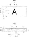
- the optical body 1 includes a base material 10 and a light extraction unit 11.
- the optical body 1 is also called a light guide plate.
- the base material 10 propagates light injected in the inside of the base material 10, that is, internally propagating light in planar directions of the base material 10 (i.e., directions perpendicular to the thickness direction; in FIG. 2 , horizontal directions). That is, the internally propagating light propagates through the inside of the base material 10 while repeating total reflection at surfaces 10A and 10B of the base material 10.
- the base material 10 is formed of a resin excellent in light conductivity, preferably a thermoplastic resin. Examples of such a resin include polymethyl methacrylate, a polycarbonate, A-PET, a cycloolefin copolymer, a cycloolefin polymer, and the like.
- the base material 10 may also be formed of an inorganic material excellent in light conductivity. Examples of such an inorganic material include silicon-based materials, more specifically glass or the like.
- the thickness of the base material 10 is not particularly limited, and may be adjusted in accordance with the use etc. of the optical body 1, as appropriate.
- the light extraction unit 11 is formed on at least one surface 10A of the base material 10. As shown in FIG. 2 and FIG. 3 , the light extraction unit 11 extracts internally propagating light, and emits the internally propagating light to the outside of the optical body 1.
- Straight line L10 of FIG. 3 shows the optical path of internally propagating light
- straight line L11 shows the optical path of light extracted to the outside, that is, extracted light. That is, internally propagating light that has arrived at the light extraction unit 11 is reflected (diffused) at a surface of the light extraction unit 11, and is emitted to the outside from surface 10B due to a light diffraction phenomenon.
- the light extraction unit 11 is formed in a place of surface 10A from which it is intended to extract light.
- a light emitting region is enabled by the turning on and off of a light source 20.
- Various designs are created by the shape of the light emitting region. In the example shown in FIG. 1 , a design of "A" of the alphabet is created. As a matter of course, the design formed by the light emitting region is not limited to this example. For example, frames, graduation marks, numerals, etc. of speedometers may be created.
- the light extraction unit 11 is formed of a convex microlens array. That is, the light extraction unit 11 includes a large number of convex microlenses 11a.
- Internally propagating light is reflected (totally reflected) at a surface of the convex microlens 11a, and is emitted to the outside of the optical body 1 from surface 10B.
- not all the internally propagating light reflected at the surface of the convex microlens 11a is emitted to the outside. That is, internally propagating light reflected at an end 11b of the convex microlens 11a or the vicinity of it is emitted to the outside.
- most of the internally propagating light reflected at the other portions of the convex microlens 11a is reflected at surface 10B again, and travels through the inside of the base material 10.
- the region of the end 11b of the convex microlens 11a and the vicinity of it functions as the light extraction unit 11.
- the end 11b forms a boundary line 11c between the convex microlenses 11a.
- the end 11b forms a boundary line between the convex microlens 11a and the base material 10.
- the maximum inclination angle ⁇ L of the convex microlens 11a is the angle between a tangent line L2 at the end 11b of the convex microlens 11a and straight line L1 (a straight line showing a planar direction of the base material 10), and is represented by Mathematical Formula (1) below.
- the propagation angle of internally propagating light is the angle ⁇ between the optical path of the internally propagating light (straight line L10) and straight line L1.
- the propagation angle ⁇ coincides with the maximum propagation angle ⁇ 0 described later.
- the light extraction efficiency is conceptually the ratio between the total light intensity of light injected in the optical body 1 from the light source 20 and the total light intensity of light emitted from the light extraction unit 11.
- the maximum inclination angle ⁇ L of the convex microlens 11a is too large, the reflection of internally propagating light at the surface of the convex microlens 11a does not satisfy the requirements of total reflection; hence, part of the internally propagating light that has arrived at the convex microlens 11a is likely to leak out from the surface of the convex microlens 11a to the outside of the optical body 1. Consequently, the light extraction efficiency is rather reduced.
- the case where the light extraction efficiency is at the maximum is a case where the maximum inclination angle ⁇ L of the convex microlens 11a substantially coincides with the maximum propagation angle ⁇ 0 of internally propagating light.
- the maximum propagation angle ⁇ 0 of internally propagating light is what is called the critical angle, and is represented by Mathematical Formula (2) below.
- p represents the pitch ( ⁇ m) of the convex microlens 11a (the distance between apices), and R represents the radius of curvature ( ⁇ m) of the convex microlens 11a.
- n represents the refractive index of the convex microlens 11a.
- the value of sin -1 is converted to the unit of degree.
- Mathematical Formula (2) it is assumed that the optical body 1 is used in air. In the case where the optical body 1 is used in an ambient environment other than air, "1" of the numerator is replaced with a refractive index in accordance with the usage environment.
- the maximum inclination angle ⁇ L of the convex microlens 11a substantially coincides with the maximum propagation angle ⁇ 0 of internally propagating light.
- the light extraction unit 11 includes a plurality of convex microlenses 11a.
- the shapes of the convex microlenses 11a are not completely the same.
- the maximum inclination angle ⁇ L of the convex microlens 11a may vary between convex microlenses 11a.
- the arithmetic average value of the maximum inclination angles ⁇ L calculated for the plurality of convex microlenses 11a is caused to substantially coincide with the maximum propagation angle ⁇ 0 .
- the arithmetic average value of the maximum inclination angles ⁇ L may be referred to as "the maximum inclination angle ⁇ Ln of the convex microlens array.”
- the maximum inclination angle ⁇ Ln of the convex microlens array substantially coincides with the maximum propagation angle ⁇ 0 .
- some (for example, several tens of) convex microlenses 11a may be picked out, and the arithmetic average value of the maximum inclination angles ⁇ L of these may be calculated.
- substantially coincide is a concept that may include not only complete coincidence but also some errors.
- the error between the maximum inclination angle ⁇ Ln of the convex microlens array and the maximum propagation angle ⁇ 0 is less than or equal to ⁇ 10 degrees, both may be regarded as substantially coinciding.
- the error between these is preferably less than or equal to ⁇ 7 degrees, more preferably less than or equal to ⁇ 5 degrees, and still more preferably less than or equal to ⁇ 3 degrees.
- the light extraction efficiency can be enhanced. Furthermore, also transmission haze is improved by such a configuration. That is, at the time of turning-off of the light source 20, the light extraction unit 11 is less likely to be seen by the observer.
- the microlenses constituting the light extraction unit 11 are "convex" microlenses 11a.
- the effect of the present embodiment is not obtained, as described in Comparative Examples described later.
- the present inventors consider that the following reason is a reason for this. Regardless of whether the microlens is convex or concave, the inclination angle of both ends of the microlens is the maximum inclination angle. In the case where the light extraction unit 11 is composed of convex microlenses 11a, a large number of both ends of convex microlenses 11a exist on the inside in the thickness direction of the optical body 1.
- both ends of the convex microlens 11a are placed on the inside in the thickness direction of the optical body 1 with respect to the other regions of the convex microlens 11a.
- the light extraction unit 11 is composed of concave microlenses
- a large number of both ends of concave microlenses exist on the surface side of the optical body 1. That is, both ends of the concave microlens protrude on the outside in the thickness direction of the optical body 1. Therefore, in the case where the light extraction unit 11 is composed of convex microlenses 11a, a larger amount of internally propagating light arrives at both ends of convex microlenses 11a, and changes the propagation angle largely. Thus, the light extraction efficiency is increased.
- the rate of filling of the convex microlens array is 100%.
- the rate of filling is the ratio of the area of convex microlenses 11a in the total area of the convex microlens array.
- the rate of filling being 100% means that the total area of the convex microlens array is occupied by convex microlenses 11a. That is, the end 11b of any of all the convex microlenses 11a constituting the convex microlens array overlaps with the end 11b of an adjacent convex microlens 11a. Thereby, the light extraction efficiency is further enhanced. Furthermore, a fine quality image with little feeling of granularity can be displayed.
- the rate of filling of the convex microlens array may be less than 100%; however, in view of the light extraction efficiency and a feeling of granularity, the rate of filling is preferably a value as close as possible to 100%.
- the rate of filling is preferably more than or equal to 70%.
- the boundary line 11c between convex microlenses 11a forms a straight line and further a polygonal shape in a planar view. Thereby, the light extraction efficiency is further enhanced. Since the convex microlenses 11a are figures similar to each other (a spherical shape) and the rate of filling is 100%, the boundary line 11c forms the shape described above.
- the pitch of the convex microlens 11a there are no particular limitations on the pitch of the convex microlens 11a; for example, it may be approximately 60 to 200 ⁇ m from the viewpoints of the ease of working, etc.
- the region of the end 11b of the convex microlens 11a and the vicinity of it functions as the light extraction unit 11.
- the convex microlens 11a it is sufficient for the convex microlens 11a to have a microlens function (that is, the function of totally reflecting internally propagating light) in the region of the end 11b and the vicinity of it.
- the light extraction unit 11 can be observed with a scanning electron microscope (SEM), a cross-sectional transmission electron microscope (cross-sectional TEM), or the like, for example.
- SEM scanning electron microscope
- cross-sectional TEM cross-sectional transmission electron microscope
- the light extraction unit 11 is molded integrally with the base material 10, for example. Although details are described later, the light extraction unit 11 can be formed on a surface of the base material 10 by, for example, forming the base material 10 out of a thermoplastic resin and transferring, to the base material 10, the surface shape of a master 100 (the surface shape of the master 100 has the inverse shape of the light extraction unit 11).
- the light extraction unit 11 may be formed as a separate body from the base material 10.
- the light extraction unit 11 is formed of a cured product of a curing resin, for example.
- the light extraction unit 11 is formed by transferring the surface shape of the master 100 to an uncured resin layer that is formed on a surface of the base material 10 in advance, and then curing the uncured resin layer. Since the light extraction unit 11 can thus be formed on one surface of the base material 10 by using one master 100, the optical body 1 can be produced easily.
- the cured product of a curing resin preferably has transparency.
- the curing resin contains a polymerizable compound and a curing initiator.
- the polymerizable compound is a resin that is cured by the curing initiator.
- Examples of the polymerizable compound include an epoxy polymerizable compound, an acrylic polymerizable compound, and the like.
- the epoxy polymerizable compound is a monomer, an oligomer, or a prepolymer containing one or two or more epoxy groups in a molecule.
- epoxy polymerizable compound various bisphenol-type epoxy resins (a bisphenol A-type, a bisphenol F-type, etc.), a novolac-type epoxy resin, various modified epoxy resins of rubber, a urethane, and the like, a naphthalene-type epoxy resin, a biphenyl-type epoxy resin, a phenol novolac-type epoxy resin, a stilbene-type epoxy resin, a triphenolmethane-type epoxy resin, a dicyclopentadiene-type epoxy resin, and a triphenylmethane-type epoxy resin, prepolymers of these, and the like are given.
- bisphenol-type epoxy resins a bisphenol A-type, a bisphenol F-type, etc.
- novolac-type epoxy resin various modified epoxy resins of rubber, a urethane, and the like
- naphthalene-type epoxy resin a biphenyl-type epoxy resin
- phenol novolac-type epoxy resin a phenol novo
- the acrylic polymerizable compound is a monomer, an oligomer, or a prepolymer containing one or two or more acryl groups in a molecule.
- the monomer is further classified into a monofunctional monomer containing one acryl group in a molecule, a bifunctional monomer containing two acryl groups in a molecule, and a polyfunctional monomer containing three or more acryl groups in a molecule.
- Examples of the "monofunctional monomer” include carboxylic acids (acrylic acid), hydroxy compounds (2-hydroxyethyl acrylate, 2-hydroxypropyl acrylate, and 4-hydroxybutyl acrylate), and alkyl or alicyclic monomers (isobutyl acrylate, t-butyl acrylate, isooctyl acrylate, lauryl acrylate, stearyl acrylate, isobornyl acrylate, and cyclohexyl acrylate), other functional monomers (2-methoxyethyl acrylate, methoxyethylene glycol acrylate, 2-ethoxyethyl acrylate, tetrahydrofurfuryl acrylate, benzyl acrylate, Ethyl Carbitol Acrylate, phenoxyethyl acrylate, N,N-dimethylaminoethyl acrylate, N,N-dimethylaminopropylacrylamide, N,N-d
- bifunctional monomer examples include tri(propylene glycol) diacrylate, trimethylolpropane diallyl ether, a urethane diacrylate, and the like.
- polyfunctional monomer examples include trimethylolpropane triacrylate, dipentaerythritol pentaacrylate and dipentaerythritol hexaacrylate, di(trimethylolpropane) tetraacrylate, and the like.
- acrylic polymerizable compounds enumerated above examples include acrylic morpholine, glycerol acrylate, a polyether-based acrylate, N-vinylformamide, N-vinylcaprolactam, ethoxydiethylene glycol acrylate, methoxytriethylene glycol acrylate, polyethylene glycol acrylate, EO-modified trimethylolpropane triacrylate, EO-modified bisphenol A diacrylate, an aliphatic urethane oligomer, a polyester oligomer, and the like.
- the polymerizable compound is preferably an acrylic polymerizable compound.
- the curing initiator is a material that cures the curing resin.
- the curing initiator include a thermosetting initiator, a light-curing initiator, and the like.
- the curing initiator may also be one that makes curing with some kind of energy ray (for example, an electron beam) or the like other than heat or light.
- the curing resin is a thermosetting resin
- the curing resin is a light-curing resin.
- the curing initiator is preferably an ultraviolet curing initiator.
- the curing resin is preferably an ultraviolet curing acrylic resin.
- the ultraviolet curing initiator is a kind of light-curing initiator. Examples of the ultraviolet curing initiator include 2,2-dimethoxy-1,2-diphenylethane-1-one, 1-hydroxycyclohexyl phenyl ketone, 2-hydroxy-2-methyl-1-phenylpropane-1-one, and the like.
- the light extraction unit 11 may be formed of a resin provided with functionality such as hydrophilicity, water repellency, demisting, etc.
- An additive in accordance with the use of the optical body 1 may be added to the light extraction unit 11.
- an additive include an inorganic filler, an organic filler, a leveling agent, a surface conditioner, an antifoaming agent, etc.
- the type of the inorganic filler include fine particles of metal oxides such as SiO 2 , TiO 2 , ZrO 2 , SnO 2 , and Al 2 O 3 .
- the light extraction unit 11 may be formed directly on the base material 10, a resin film (for example, a thermoplastic resin film) on which the light extraction unit 11 is formed may be adhered to the base material 10.
- a resin film for example, a thermoplastic resin film
- an antireflection structure is formed in regions of both surfaces of the base material 10 where the light extraction unit 11 is not formed.
- the antireflection structure include a micro concave-convex structure in which the average period of concavity and convexity is less than the smallest value of the wavelengths of visible light (what is called a moth-eye structure), a structure in which a high refractive index film and a low refractive index film are alternately stacked (an AR multiple-layer film), etc.
- the method for manufacturing an antireflection structure is not particularly limited, and the antireflection structure may be formed on the surface of the base material 10 by a method similar to conventional manufacturing methods.
- the micro concave-convex structure can be formed on the surface of the base material 10 by a method similar to a method for manufacturing the light extraction unit 11.
- the light emitting device includes the optical body 1 described above and the light source 20.
- the type of the light source 20 is not particularly questioned, and may be a light source used for conventional light guide plates. That is, the light source 20 may be one that emits white light or one that emits monochromatic light.
- the operation of the light emitting device is roughly as follows. First, light is incident on the optical body 1 from the light source 20. The light injected in the inside of the optical body 1, that is, internally propagating light propagates through the inside of the optical body 1 while reflecting at both surfaces of the optical body 1 (that is, interfaces between the inside and the outside of the optical body 1).
- Part of the internally propagating light arrives at the light extraction unit 11.
- the internally propagating light that has arrived at the light extraction unit 11 is totally reflected at a surface of the light extraction unit 11, that is, a surface of the convex microlens 11a, and is emitted to the outside of the optical body 1 from surface 10B.
- the observer visually identifies the light emitting device from the surface 10B side.
- the maximum inclination angle ⁇ Ln of the convex microlens array substantially coincides with the maximum propagation angle ⁇ 0 , the light extraction efficiency is enhanced.
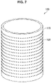
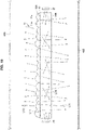
- the light extraction unit 11 is produced using, for example, a master 100 shown in FIG. 7 .
- the master 100 is a master used in the nanoimprinting method, and has a round cylindrical shape, for example.
- the master 100 may have a round columnar shape or other shapes (for example, a flat plate-like shape).
- a concave-convex structure that is, a master concave-convex structure
- a concave-convex structure 120 of the master 100 can be transferred seamlessly to a resin base material or the like by a roll-to-roll system.
- the optical body 1 to which the master concave-convex structure 120 of the master 100 has been transferred can be produced with high production efficiency.
- the shape of the master 100 is preferably a round cylindrical shape or a round columnar shape.
- the master 100 is provided with a master base material 110, and the master concave-convex structure 120 formed on the circumferential surface of the master base material 110.
- the master base material 110 is a glass body, for example, and specifically is formed from quartz glass.
- the master base material 110 is not particularly limited insofar as the SiO 2 purity is high, and may also be formed from a material such as fused quartz glass or synthetic quartz glass.
- the master base material 110 may also be a laminate of the above materials on a metal matrix, or a metal matrix.
- the shape of the master base material 110 is a hollow round cylindrical shape, but may also be a round columnar shape, or some other shape. However, as described above, the master base material 110 preferably has a hollow round cylindrical shape or a round columnar shape.
- the master concave-convex structure 120 has the inverse shape of the surface shape of the optical body 1 (for example, the inverse shape of the light extraction unit 11 to be formed on one surface 10A of the base material 10).
- a base material resist layer is formed (deposited) on the master base material 110.
- the resist constituting the base material resist layer is not particularly limited, and may be either an organic resist or an inorganic resist.
- organic resists include novolac-type resist and chemically-amplified resist.
- inorganic resists include metallic oxides including one or multiple types of transition metals such as tungsten (W) or molybdenum (Mo).
- W tungsten
- Mo molybdenum
- the base material resist layer preferably is formed with a thermo-reactive resist including a metallic oxide.
- the base material resist layer may be formed on the master base material 110 by using a process such as spin coating, slit coating, dip coating, spray coating, or screen printing. Also, in the case of using an inorganic resist for the base material resist layer, the base material resist layer may be formed by sputtering.
- a latent image is formed on the base material resist layer.
- the exposure device 200 modulates laser light 200A, and irradiates the base material resist layer with the laser light 200A. Consequently, part of the base material resist layer irradiated by the laser light 200A denatures, and thus a latent image corresponding to the master concave-convex structure 120 may be formed in the base material resist layer.
- the base material resist layer is developed.
- a concave-convex structure is formed in the base material resist layer.
- the master concave-convex structure 120 is formed on the master base material 110.
- the etching method is not particularly limited, dry etching that is vertically anisotropic is preferable. For example, reactive ion etching (RIE) is preferable.
- anodic porous alumina obtained by the anodic oxidation of aluminum may also be used as the master.
- Anodic porous alumina is disclosed in WO 2006/059686 , for example.
- the master 100 may also be produced by a stepper using a reticle mask with an asymmetric shape.
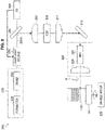
- the exposure device 200 is a device that exposes the base material resist layer.
- the exposure device 200 is provided with a laser light source 201, a first mirror 203, a photodiode (PD) 205, a deflecting optical system, a control mechanism 230, a second mirror 213, a movable optical table 220, a spindle motor 225, and a turntable 227.
- the master base material 110 is placed on the turntable 227 and able to be rotated.
- the laser light source 201 is a light source that emits laser light 200A, and is a device such as a solid-state laser or a semiconductor laser, for example.
- the wavelength of the laser light 200A emitted by the laser light source 201 is not particularly limited, but may be a wavelength in the blue light band from 400 nm to 500 nm, for example. Also, it is sufficient for the spot diameter of the laser light 200A (the diameter of the spot radiated onto the resist layer) to be smaller than the diameter of the open face of a concavity of the master concave-convex structure 120, such as approximately 200 nm, for example.
- the laser light 200A emitted from the laser light source 201 is controlled by the control mechanism 230.
- the laser light 200A emitted from the laser light source 201 advances directly in a collimated beam, reflects off the first mirror 203, and is guided to the deflecting optical system.
- the first mirror 203 is made up of a polarizing beam splitter, and has a function of reflecting one polarized component, and transmitting the other polarized component.
- the polarized component transmitted through the first mirror 203 is sensed by the photodiode 205 and photoelectrically converted.
- the photodetection signal photoelectrically converted by the photodiode 205 is input into the laser light source 201, and the laser light source 201 conducts phase modulation of the laser light 200A on the basis of the input photodetection signal.
- the deflecting optical system is provided with a condenser lens 207, an electro-optic deflector (EOD) 209, and a collimator lens 211.
- EOD electro-optic deflector
- the laser light 200A is condensed onto the electro-optic deflector 209 by the condenser lens 207.
- the electro-optic deflector 209 is an element capable of controlling the radiation position of the laser light 200A.
- the exposure device 200 is also able to vary the radiation position of the laser light 200A guided onto the movable optical table 220 (what is called a Wobble mechanism).
- the laser light 200A is converted back into a collimated beam by the collimator lens 211.
- the laser light 200A exiting the deflecting optical system is reflected by the second mirror 213, and guided level with and parallel to the movable optical table 220.
- the movable optical table 220 is provided with a beam expander (BEX) 221 and an objective lens 223.
- the laser light 200A guided to the movable optical table 220 is shaped into a desired beam shape by the beam expander 221, and then radiated via the objective lens 223 onto the base material resist layer formed on the master base material 110.
- the movable optical table 220 moves by one feed pitch (track pitch) in the direction of the arrow R (feed pitch direction) every time the master base material 110 undergoes one rotation.
- the master base material 110 is placed on the turntable 227.
- the spindle motor 225 causes the turntable 227 to rotate, thereby causing the master base material 110 to rotate.
- the laser light 200A is made to scan over the base material resist layer. At this point, a latent image of the base material resist layer is formed along the scanning direction of the laser light 200A.
- control mechanism 230 is provided with a formatter 231 and a driver 233, and controls the radiation of the laser light 200A.
- the formatter 231 generates a modulation signal that controls the radiation of the laser light 200A
- the driver 233 controls the laser light source 201 on the basis of the modulation signal generated by the formatter 231. As a result, the irradiation of the master base material 110 by the laser light 200A is controlled.
- the formatter 231 generates a control signal for irradiating the base material resist layer with the laser light 200A, on the basis of an input image depicting an arbitrary pattern to draw on the base material resist layer. Specifically, first, the formatter 231 acquires an input image depicting an arbitrary draw pattern to draw on the base material resist layer.
- the input image is an image corresponding to a development of the outer circumferential surface of the base material resist layer, in which the outer circumferential surface of the base material resist layer is cut in the axial direction and expanded in a single plane. In this development, an image corresponding to the circumferential shape of the master 100 is depicted. This image shows the inverse shape of the surface shape of the optical body 1.
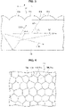
- An example of the input image is shown in FIG. 6 . Further, a perspective image corresponding to FIG. 6 is shown in FIG. 5 .
- the formatter 231 partitions the input image into sub-regions of a certain size (for example, partitions the input image into a lattice), and determines whether or not the concavity draw pattern (that is a pattern that corresponds to the concavity of the master 100) is included in each of the sub-regions. Subsequently, the formatter 231 generates a control signal to perform control to irradiate with the laser light 200A each sub-region determined to include the concavity draw pattern.
- the control signal (that is, the exposure signal) preferably is synchronized with the rotation of the spindle motor 225, but does not have to be synchronized.
- control signal and the rotation of the spindle motor 225 may also be resynchronized every time the master base material 110 performs one rotation.
- the driver 233 controls the output of the laser light source 201 on the basis of the control signal generated by the formatter 231. As a result, the irradiation of the base material resist layer by the laser light 200A is controlled.
- the exposure device 200 may also perform a known exposure control process, such as focus servo and positional correction of the irradiation spot of the laser light 200A.
- the focus servo may use the wavelength of the laser light 200A, or use another wavelength for reference.
- the laser light 200A radiated from the laser light source 201 may irradiate the base material resist layer after being split into multiple optical subsystems. In this case, multiple irradiation spots are formed on the base material resist layer. In this case, when the laser light 200A emitted from one optical system reaches the latent image formed by another optical system, exposure may be ended.
- a latent image in accordance with a draw pattern of an input image can be formed on a resist layer. Then, the resist layer is developed, and the resist layer after development is used as a mask to etch the master base material 110 and the base material resist layer; thereby, a master concave-convex structure 120 in accordance with the draw pattern of the input image is formed on the master base material 110. That is, an arbitrary master concave-convex structure 120 in accordance with a draw pattern can be formed. Therefore, when a draw pattern in which the inverse shape of the optical body 1 is depicted is prepared as a draw pattern, a master concave-convex structure 120 having the inverse shape of the optical body 1 can be formed.
- the optical body 1 can be manufactured by a transfer device 300 of a roll-to-roll system using the master 100.
- the optical body 1 is produced using a light-curing resin.
- the transfer device 300 is provided with the master 100, a base material supply roll 301, a take-up roll 302, guide rolls 303 and 304, a nip roll 305, a separation roll 306, an applicator device 307, and a light source 309.
- the base material supply roll 301 is a roll around which a long-length base material 10 is wound in a roll
- the take-up roll 302 is a roll that take the optical body 1.
- the guide rolls 303 and 304 are rolls that transport the base material 10.
- the nip roll 305 is a roll that puts the base material 10 laminated with an uncured resin layer 310, or in other words a transfer film 3a, in close contact with the master 100.
- the separation roll 306 is a roll that separates the optical body 1 from the master 100.
- the applicator device 307 is provided with an applicating means such as a coater, and applies an uncured light-curing resin composition to the base material 10, and forms the uncured resin layer 310.
- the applicator device 307 may be a device such as a gravure coater, a wire bar coater, or a die coater, for example.
- the light source 309 is a light source that emits light of a wavelength able to cure the light-curing resin composition, and may be a device such as an ultraviolet lamp, for example.
- the base material 10 is sent continuously from the base material supply roll 301 via the guide roll 303.
- the base material supply roll 301 may also be changed to a base material supply roll 301 of a separate lot.
- the uncured light-curing resin composition is applied by the applicator device 307 to the delivered base material 10, and the uncured resin layer 310 is laminated onto the base material 10.
- the transfer film 3a is prepared.
- the transfer film 3a is put into close contact with the master 100 by the nip roll 305.
- the light source 309 irradiates with light the uncured resin layer 310 put in close contact with the master 100, thereby curing the uncured resin layer 310.
- the arrangement pattern of the master concave-convex structure 120 formed on the outer circumferential face of the master 100 is transferred to the uncured resin layer 310.
- a concave-convex structure having the inverse shape of the master concave-convex structure 120 is formed on the base material 10.
- the base material 10 in which the concave-convex structure is formed that is the optical body 1
- the optical body 1 is taken up by the take-up roll 302 via the guide roll 304.
- the master 100 may be oriented vertically or oriented horizontally, and a mechanism that corrects the angle and eccentricity of the master 100 during rotation may also be provided separately.
- an eccentric tilt mechanism may be provided in a chucking mechanism.
- the transfer film 3a is transported by roll-to-roll, and on the other hand the circumferential shape of the master 100 is transferred to the transfer film 3a. Thereby, the optical body 1 is produced.
- the applicator device 307 and the light source 309 are not needed.
- a thermoplastic resin film is used as the base material 10, and a heating device is placed on the upstream side of the master 100. The base material 10 is heated and softened by the heating device, and then the base material 10 is pressed against the master 100. Thereby, the master concave-convex structure 120 formed on the circumferential surface of the master 100 is transferred to the base material 10.
- a film formed of a resin other than thermoplastic resins may be used as the base material 10, and the base material 10 and a thermoplastic resin film may be stacked.
- the stacked film is heated by a heating device, and is then pressed against the master 100.
- the transfer device 300 can continuously produce a transfer copy to which the master concave-convex structure 120 formed on the master 100 has been transferred, that is, the optical body 1.
- a transfer film to which the master concave-convex structure 120 of the master 100 has been transferred may be produced, and the transfer film may be used as a transfer mold to produce the optical body 1.
- the master 100 may be duplicated by electroforming, thermal transfer, or the like, and the duplicate may be used as a transfer mold.
- the shape of the master 100 is not necessarily limited to a roll shape, and may also be a planar master.
- various processing methods can be selected, such as semiconductor exposure using a mask, electron beam lithography, machining, or anodic oxidation.
- a resin film in which the light extraction unit 11 is formed by the manufacturing method described above may be stuck to both surfaces of the base material 10.
- Test Examples of the present embodiment are described.
- simulations were performed to verify the effect of the present embodiment.
- the base conditions of the present simulations are described on the basis of FIG. 10 .
- Zemax OpticStudio manufactured by Zemax, LLC was used as a simulation software application. That is, an electronic computer was operated by the simulation software application to perform a simulation.
- An acrylic plate 0.8 mm long ⁇ 0.7 mm wide ⁇ 0.3 mm thick was used as the base material 10.
- 17 convex microlenses 11a were arranged in a closest packing structure in which the distance between the apices of lenses (the pitch) was 60 to 100 ⁇ m (a regular arrangement of hexagonal closest packing with a rate of filling of 100%), as the light extraction unit 11 (a convex microlens array).
- the material of the convex microlens array was assumed to be an acrylic.
- Light sources 20 were arranged in positions 0.02 mm distant from the end surfaces of four sides of the base material 10 in the directions normal to the end surfaces, respectively.
- the size of the light source 20 was set to 0.6 mm long ⁇ 0.02 mm wide, and the flat surface portion was made to face the respective end surface of the base material 10.
- the radiation angle of the light source 20 was set to 60 degrees as the full width at half maximum.
- the total light intensity of light emitted from each light source 20 was fixed between all the tests.
- Light receiving surfaces 400 each with a length of 1.2 mm ⁇ a width of 1.2 mm were arranged in positions 2.0 mm distant from surface 10A (the front surface side) and surface 10B (the back surface side) of the base material 10 in the directions normal to these surfaces, respectively.
- the light receiving surface was made to face the respective surface of the base material 10. Then, the total light intensity on each light receiving surface 400 was measured as an index of light extraction efficiency.
- Test Example 1 corresponding relationship between maximum inclination angle and maximum propagation angle>
- Test Example 1 the corresponding relationship between the maximum inclination angle ⁇ Ln of the convex microlens array and the maximum propagation angle ⁇ 0 was investigated. Specifically, the pitch was fixed to either of 80 ⁇ m and 100 ⁇ m; and the radius of curvature of the convex microlens 11a was changed, and thereby the maximum inclination angle ⁇ Ln of the convex microlens array was changed. The arithmetic average value of the maximum inclination angles ⁇ L of the 17 convex microlenses 11a was used as the maximum inclination angle ⁇ Ln of the convex microlens array.
- the total light intensity is largest in the case where the maximum inclination angle ⁇ Ln of the convex microlens array has an error with the maximum propagation angle ⁇ 0 of less than or equal to ⁇ 3 degrees, and the total light intensity decreases as the error between these transitions from less than or equal to ⁇ 5 degrees, to less than or equal to ⁇ 7 degrees, and to less than or equal to ⁇ 10 degrees.
- the maximum inclination angle ⁇ Ln of the convex microlens array is approximately 70 degrees.
- the light extraction efficiency is small.
- Test Example 2 corresponding relationship between polarity (concavity or convexity) of microlens and total light intensity>
- the corresponding relationship between the polarity (concavity or convexity) of the microlens and the total light intensity was investigated. Specifically, the convex microlens 11a of a base condition was changed to a concave microlens, and processing similar to Test Example 1 was performed. The pitch was set to 100 ⁇ m. For comparison, processing similar to Test Example 1 was performed. In Test Example 2, the total light intensity not only on the back surface side but also on the front surface side was measured. Straight line L12 of FIG. 10 shows the optical path of light emitted on the front surface side. The results are shown in FIG. 12 . The definitions of the vertical axis and the horizontal axis of FIG. 12 are similar to those of FIG. 11 .
- the rate of filling was set to 100% or 70%, and processing similar to Test Example 1 was performed.
- the pitch was fixed to 100 ⁇ m.
- the maximum value of the total light intensity (the maximum light intensity) at the time of the rate of filling of 100% was larger (approximately 1.3 times) than the maximum light intensity at the time of the rate of filling of 70%. That is, the light extraction efficiency at the time of the rate of filling of 100% was larger than the light extraction efficiency at the time of the rate of filling of 70%.
- the maximum light intensity at the time of the rate of filling of 70% was larger than those in Comparative Examples 1 and 2.
Description
- This application is based upon and claims benefit of priority from
Japanese Patent Application No. 2017-191540, filed on September 29, 2017 - The present invention relates to an optical body and a light emitting device.
- As a kind of optical body, there is known an optical body in which a light waveguiding phenomenon and a light diffusion phenomenon are combined, for example as disclosed in
JP 2012-136199A - The light guide plate is used as, for example, light emitting bodies for various display devices or light emitting bodies for illumination. Examples of the display device in which a light guide plate is used include various LCDs (for example, an LCD of a local dimming driving system), passive-type display devices, light ornamentation panels for amusement, illumination panels for advertisements such as digital signage, etc. In these display devices, an expression looking as if light stood out from a region where a pattern of the light extraction unit is formed, that is, a light emitting region is enabled by the turning on and off of the light source. Various designs (numerals of speedometers, etc.) are created by the shape of the light emitting region.
- The U.S. patent application publication
US 2008/266874 A1 describes an optical plate that includes at least one transparent plate unit. The transparent plate unit includes a first surface, a second surface, a plurality of conical frustum protrusions, a plurality of spherical protrusions and a lamp-receiving portion. The second surface is opposite to the first surface. The conical frustum protrusions are formed at the first surface. The spherical protrusions are formed at the second surface. The lamp-receiving portion is defined in at least one of the first surface and the second surface. - The U.S. patent publication
US 6,174,064 B1 describes a light guide panel that includes a front surface portion, a back surface portion located on the opposite side of the front surface portion, and an incidence end surface portion located on one side of the front and the back surface portions. The incidence end surface portion is configured for introducing light from a light source into the light guide panel. A plurality of optical elements is randomly disposed on the front and/or back surface portions. The optical elements typically have a maximum diameter in a range from 10 µm to 150 µm and are configured for emanating light propagating in the light guide panel from the front surface portion and/or back surface portion to the outside of the light guide panel. - The invention is set forth in the appended claims.
-
-
FIG. 1 is a plan view showing a rough configuration of an optical body according to an embodiment of the present invention; -
FIG. 2 is a side cross-sectional view showing a cross-sectional structure of the optical body according to the embodiment; -
FIG. 3 is an enlarged side cross-sectional view of a part ofFIG. 2 ; -
FIG. 4 is an enlarged plan view of a part ofFIG. 1 ; -
FIG. 5 is a perspective image showing an example of a layout of a convex microlens array; -
FIG. 6 is a plan image showing the example of the layout of the convex microlens array; -
FIG. 7 is a perspective diagram illustrating an exemplary appearance of a master according to the present embodiment; -
FIG. 8 is a block diagram illustrating an exemplary configuration of an exposure device; -
FIG. 9 is a schematic diagram illustrating an example of a transfer device that manufactures an optical body by roll-to-roll; -
FIG. 10 is a side cross-sectional view conceptually showing a manner of a simulation performed in Examples; -
FIG. 11 is a graph showing corresponding relationships between a maximum inclination angle of a convex microlens array and a light intensity; and -
FIG. 12 is a graph showing corresponding relationships between a maximum inclination angle of a convex or concave microlens array and a light intensity. - Hereinafter, referring to the appended drawings, preferred embodiments of the present invention will be described in detail. It should be noted that, in this specification and the appended drawings, structural elements that have substantially the same function and structure are denoted with the same reference numerals, and repeated explanation thereof is omitted.
- Next, the configuration of an
optical body 1 according to the present embodiment is described on the basis ofFIG. 1 to FIG. 4 . Theoptical body 1 includes abase material 10 and alight extraction unit 11. Theoptical body 1 is also called a light guide plate. - The
base material 10 propagates light injected in the inside of thebase material 10, that is, internally propagating light in planar directions of the base material 10 (i.e., directions perpendicular to the thickness direction; inFIG. 2 , horizontal directions). That is, the internally propagating light propagates through the inside of thebase material 10 while repeating total reflection atsurfaces base material 10. Hence, thebase material 10 is formed of a resin excellent in light conductivity, preferably a thermoplastic resin. Examples of such a resin include polymethyl methacrylate, a polycarbonate, A-PET, a cycloolefin copolymer, a cycloolefin polymer, and the like. Thebase material 10 may also be formed of an inorganic material excellent in light conductivity. Examples of such an inorganic material include silicon-based materials, more specifically glass or the like. The thickness of thebase material 10 is not particularly limited, and may be adjusted in accordance with the use etc. of theoptical body 1, as appropriate. - The
light extraction unit 11 is formed on at least onesurface 10A of thebase material 10. As shown inFIG. 2 andFIG. 3 , thelight extraction unit 11 extracts internally propagating light, and emits the internally propagating light to the outside of theoptical body 1. Straight line L10 ofFIG. 3 shows the optical path of internally propagating light, and straight line L11 shows the optical path of light extracted to the outside, that is, extracted light. That is, internally propagating light that has arrived at thelight extraction unit 11 is reflected (diffused) at a surface of thelight extraction unit 11, and is emitted to the outside fromsurface 10B due to a light diffraction phenomenon. Thelight extraction unit 11 is formed in a place ofsurface 10A from which it is intended to extract light. An expression looking as if light stood out from a region where a pattern of thelight extraction unit 11 is formed, that is, a light emitting region is enabled by the turning on and off of alight source 20. Various designs are created by the shape of the light emitting region. In the example shown inFIG. 1 , a design of "A" of the alphabet is created. As a matter of course, the design formed by the light emitting region is not limited to this example. For example, frames, graduation marks, numerals, etc. of speedometers may be created. - Here, the configuration of the
light extraction unit 11 is described in detail on the basis ofFIG. 2 to FIG. 4 . Thelight extraction unit 11 is formed of a convex microlens array. That is, thelight extraction unit 11 includes a large number ofconvex microlenses 11a. - Internally propagating light is reflected (totally reflected) at a surface of the
convex microlens 11a, and is emitted to the outside of theoptical body 1 fromsurface 10B. Here, not all the internally propagating light reflected at the surface of theconvex microlens 11a is emitted to the outside. That is, internally propagating light reflected at anend 11b of theconvex microlens 11a or the vicinity of it is emitted to the outside. On the other hand, most of the internally propagating light reflected at the other portions of theconvex microlens 11a is reflected atsurface 10B again, and travels through the inside of thebase material 10. Thus, the region of theend 11b of theconvex microlens 11a and the vicinity of it functions as thelight extraction unit 11. Here, in the case where the ends 11b of adjacentconvex microlenses 11a overlap, theend 11b forms aboundary line 11c between theconvex microlenses 11a. In the case where adjacentconvex microlenses 11a are apart, theend 11b forms a boundary line between theconvex microlens 11a and thebase material 10. - As shown in
FIG. 3 , as the maximum inclination angle θL of theconvex microlens 11a becomes larger, the change in the propagation angle of internally propagating light becomes larger when the internally propagating light is reflected at the surface of theconvex microlens 11a. Hence, the light extraction efficiency (radiation efficiency) is increased. Here, the maximum inclination angle θL of theconvex microlens 11a is the angle between a tangent line L2 at theend 11b of theconvex microlens 11a and straight line L1 (a straight line showing a planar direction of the base material 10), and is represented by Mathematical Formula (1) below. The propagation angle of internally propagating light is the angle θ between the optical path of the internally propagating light (straight line L10) and straight line L1. InFIG. 3 , the propagation angle θ coincides with the maximum propagation angle θ0 described later. The light extraction efficiency is conceptually the ratio between the total light intensity of light injected in theoptical body 1 from thelight source 20 and the total light intensity of light emitted from thelight extraction unit 11. - On the other hand, if the maximum inclination angle θL of the
convex microlens 11a is too large, the reflection of internally propagating light at the surface of theconvex microlens 11a does not satisfy the requirements of total reflection; hence, part of the internally propagating light that has arrived at theconvex microlens 11a is likely to leak out from the surface of theconvex microlens 11a to the outside of theoptical body 1. Consequently, the light extraction efficiency is rather reduced. - Therefore, it can be said that the case where the light extraction efficiency is at the maximum is a case where the maximum inclination angle θL of the
convex microlens 11a substantially coincides with the maximum propagation angle θ0 of internally propagating light. Here, the maximum propagation angle θ0 of internally propagating light is what is called the critical angle, and is represented by Mathematical Formula (2) below.
[Math. 1]
[Math. 2]
- In Mathematical Formula (1), p represents the pitch (µm) of the
convex microlens 11a (the distance between apices), and R represents the radius of curvature (µm) of theconvex microlens 11a. In Mathematical Formula (2), n represents the refractive index of theconvex microlens 11a. In Mathematical Formulae (1) and (2), the value of sin-1 is converted to the unit of degree. In Mathematical Formula (2), it is assumed that theoptical body 1 is used in air. In the case where theoptical body 1 is used in an ambient environment other than air, "1" of the numerator is replaced with a refractive index in accordance with the usage environment. InFIG. 3 , the maximum inclination angle θL of theconvex microlens 11a substantially coincides with the maximum propagation angle θ0 of internally propagating light. - Here, the
light extraction unit 11 includes a plurality ofconvex microlenses 11a. For reasons of manufacturing errors etc., the shapes of theconvex microlenses 11a are not completely the same. Also a case where the shape of theconvex microlens 11a is varied intentionally is envisaged. Therefore, the maximum inclination angle θL of theconvex microlens 11a may vary betweenconvex microlenses 11a. Thus, in the present embodiment, the arithmetic average value of the maximum inclination angles θL calculated for the plurality ofconvex microlenses 11a is caused to substantially coincide with the maximum propagation angle θ0. Hereinafter, the arithmetic average value of the maximum inclination angles θL may be referred to as "the maximum inclination angle θLn of the convex microlens array." - Thus, in the present embodiment, the maximum inclination angle θLn of the convex microlens array substantially coincides with the maximum propagation angle θ0. When calculating the maximum inclination angle θLn of the convex microlens array, some (for example, several tens of)
convex microlenses 11a may be picked out, and the arithmetic average value of the maximum inclination angles θL of these may be calculated. - "Substantially coincide" is a concept that may include not only complete coincidence but also some errors. For example, when the error between the maximum inclination angle θLn of the convex microlens array and the maximum propagation angle θ0 is less than or equal to ±10 degrees, both may be regarded as substantially coinciding. In order for the maximum inclination angle θLn of the convex microlens array and the maximum propagation angle θ0 to substantially coincide, the error between these is preferably less than or equal to ±7 degrees, more preferably less than or equal to ±5 degrees, and still more preferably less than or equal to ±3 degrees.
- In the present embodiment, since the maximum inclination angle θLn of the convex microlens array substantially coincides with the maximum propagation angle θ0, the light extraction efficiency can be enhanced. Furthermore, also transmission haze is improved by such a configuration. That is, at the time of turning-off of the
light source 20, thelight extraction unit 11 is less likely to be seen by the observer. - The microlenses constituting the
light extraction unit 11 are "convex"microlenses 11a. In the case where thelight extraction unit 11 is composed of concave microlenses, the effect of the present embodiment is not obtained, as described in Comparative Examples described later. The present inventors consider that the following reason is a reason for this. Regardless of whether the microlens is convex or concave, the inclination angle of both ends of the microlens is the maximum inclination angle. In the case where thelight extraction unit 11 is composed ofconvex microlenses 11a, a large number of both ends ofconvex microlenses 11a exist on the inside in the thickness direction of theoptical body 1. That is, both ends of theconvex microlens 11a are placed on the inside in the thickness direction of theoptical body 1 with respect to the other regions of theconvex microlens 11a. On the other hand, in the case where thelight extraction unit 11 is composed of concave microlenses, a large number of both ends of concave microlenses exist on the surface side of theoptical body 1. That is, both ends of the concave microlens protrude on the outside in the thickness direction of theoptical body 1. Therefore, in the case where thelight extraction unit 11 is composed ofconvex microlenses 11a, a larger amount of internally propagating light arrives at both ends ofconvex microlenses 11a, and changes the propagation angle largely. Thus, the light extraction efficiency is increased. - As shown in
FIG. 4 , the rate of filling of the convex microlens array is 100%. Here, the rate of filling is the ratio of the area ofconvex microlenses 11a in the total area of the convex microlens array. The rate of filling being 100% means that the total area of the convex microlens array is occupied byconvex microlenses 11a. That is, theend 11b of any of all theconvex microlenses 11a constituting the convex microlens array overlaps with theend 11b of an adjacentconvex microlens 11a. Thereby, the light extraction efficiency is further enhanced. Furthermore, a fine quality image with little feeling of granularity can be displayed. As a matter of course, the rate of filling of the convex microlens array may be less than 100%; however, in view of the light extraction efficiency and a feeling of granularity, the rate of filling is preferably a value as close as possible to 100%. For example, the rate of filling is preferably more than or equal to 70%. - As shown in the drawing, the
boundary line 11c betweenconvex microlenses 11a forms a straight line and further a polygonal shape in a planar view. Thereby, the light extraction efficiency is further enhanced. Since theconvex microlenses 11a are figures similar to each other (a spherical shape) and the rate of filling is 100%, theboundary line 11c forms the shape described above. - There are no particular limitations on the pitch of the
convex microlens 11a; for example, it may be approximately 60 to 200 µm from the viewpoints of the ease of working, etc. - As described above, the region of the
end 11b of theconvex microlens 11a and the vicinity of it functions as thelight extraction unit 11. Thus, it is sufficient for theconvex microlens 11a to have a microlens function (that is, the function of totally reflecting internally propagating light) in the region of theend 11b and the vicinity of it. - The
light extraction unit 11 can be observed with a scanning electron microscope (SEM), a cross-sectional transmission electron microscope (cross-sectional TEM), or the like, for example. - Here, the
light extraction unit 11 is molded integrally with thebase material 10, for example. Although details are described later, thelight extraction unit 11 can be formed on a surface of thebase material 10 by, for example, forming thebase material 10 out of a thermoplastic resin and transferring, to thebase material 10, the surface shape of a master 100 (the surface shape of themaster 100 has the inverse shape of the light extraction unit 11). - On the other hand, the
light extraction unit 11 may be formed as a separate body from thebase material 10. In this case, thelight extraction unit 11 is formed of a cured product of a curing resin, for example. Although details are described later, thelight extraction unit 11 is formed by transferring the surface shape of themaster 100 to an uncured resin layer that is formed on a surface of thebase material 10 in advance, and then curing the uncured resin layer. Since thelight extraction unit 11 can thus be formed on one surface of thebase material 10 by using onemaster 100, theoptical body 1 can be produced easily. - The cured product of a curing resin preferably has transparency. The curing resin contains a polymerizable compound and a curing initiator. The polymerizable compound is a resin that is cured by the curing initiator. Examples of the polymerizable compound include an epoxy polymerizable compound, an acrylic polymerizable compound, and the like. The epoxy polymerizable compound is a monomer, an oligomer, or a prepolymer containing one or two or more epoxy groups in a molecule. As the epoxy polymerizable compound, various bisphenol-type epoxy resins (a bisphenol A-type, a bisphenol F-type, etc.), a novolac-type epoxy resin, various modified epoxy resins of rubber, a urethane, and the like, a naphthalene-type epoxy resin, a biphenyl-type epoxy resin, a phenol novolac-type epoxy resin, a stilbene-type epoxy resin, a triphenolmethane-type epoxy resin, a dicyclopentadiene-type epoxy resin, and a triphenylmethane-type epoxy resin, prepolymers of these, and the like are given.
- The acrylic polymerizable compound is a monomer, an oligomer, or a prepolymer containing one or two or more acryl groups in a molecule. Here, the monomer is further classified into a monofunctional monomer containing one acryl group in a molecule, a bifunctional monomer containing two acryl groups in a molecule, and a polyfunctional monomer containing three or more acryl groups in a molecule.
- Examples of the "monofunctional monomer" include carboxylic acids (acrylic acid), hydroxy compounds (2-hydroxyethyl acrylate, 2-hydroxypropyl acrylate, and 4-hydroxybutyl acrylate), and alkyl or alicyclic monomers (isobutyl acrylate, t-butyl acrylate, isooctyl acrylate, lauryl acrylate, stearyl acrylate, isobornyl acrylate, and cyclohexyl acrylate), other functional monomers (2-methoxyethyl acrylate, methoxyethylene glycol acrylate, 2-ethoxyethyl acrylate, tetrahydrofurfuryl acrylate, benzyl acrylate, Ethyl Carbitol Acrylate, phenoxyethyl acrylate, N,N-dimethylaminoethyl acrylate, N,N-dimethylaminopropylacrylamide, N,N-dimethylacrylamide, acryloylmorpholine, N-isopropylacrylamide, N,N-diethylacrylamide, 2-(perfluorooctyl)ethyl acrylate, 3-perfluorohexyl-2-hydroxypropyl acrylate, 3-perfluorooctyl-2-hydroxypropyl acrylate, 2-(perfluorodecyl)ethyl acrylate, 2-(perfluoro-3-methylbutyl)ethyl acrylate, 2,4,6-tribromophenol acrylate, 2,4,6-tribromophenol methacrylate, 2-(2,4,6-tribromophenoxy)ethyl acrylate, and 2-ethylhexyl acrylate), and the like.
- Examples of the "bifunctional monomer" include tri(propylene glycol) diacrylate, trimethylolpropane diallyl ether, a urethane diacrylate, and the like.
- Examples of the "polyfunctional monomer" include trimethylolpropane triacrylate, dipentaerythritol pentaacrylate and dipentaerythritol hexaacrylate, di(trimethylolpropane) tetraacrylate, and the like.
- Examples other than the acrylic polymerizable compounds enumerated above include acrylic morpholine, glycerol acrylate, a polyether-based acrylate, N-vinylformamide, N-vinylcaprolactam, ethoxydiethylene glycol acrylate, methoxytriethylene glycol acrylate, polyethylene glycol acrylate, EO-modified trimethylolpropane triacrylate, EO-modified bisphenol A diacrylate, an aliphatic urethane oligomer, a polyester oligomer, and the like. From the viewpoint of the transparency of the
optical body 1, the polymerizable compound is preferably an acrylic polymerizable compound. - The curing initiator is a material that cures the curing resin. Examples of the curing initiator include a thermosetting initiator, a light-curing initiator, and the like. The curing initiator may also be one that makes curing with some kind of energy ray (for example, an electron beam) or the like other than heat or light. In the case where the curing initiator is a thermosetting initiator, the curing resin is a thermosetting resin; in the case where the curing initiator is a light-curing initiator, the curing resin is a light-curing resin.
- Here, from the viewpoint of the transparency of the
optical body 1, the curing initiator is preferably an ultraviolet curing initiator. Accordingly, the curing resin is preferably an ultraviolet curing acrylic resin. The ultraviolet curing initiator is a kind of light-curing initiator. Examples of the ultraviolet curing initiator include 2,2-dimethoxy-1,2-diphenylethane-1-one, 1-hydroxycyclohexyl phenyl ketone, 2-hydroxy-2-methyl-1-phenylpropane-1-one, and the like. - The
light extraction unit 11 may be formed of a resin provided with functionality such as hydrophilicity, water repellency, demisting, etc. - An additive in accordance with the use of the
optical body 1 may be added to thelight extraction unit 11. Examples of such an additive include an inorganic filler, an organic filler, a leveling agent, a surface conditioner, an antifoaming agent, etc. Examples of the type of the inorganic filler include fine particles of metal oxides such as SiO2, TiO2, ZrO2, SnO2, and Al2O3. - Although the
light extraction unit 11 may be formed directly on thebase material 10, a resin film (for example, a thermoplastic resin film) on which thelight extraction unit 11 is formed may be adhered to thebase material 10. - In accordance with the invention, an antireflection structure is formed in regions of both surfaces of the
base material 10 where thelight extraction unit 11 is not formed. Examples of the antireflection structure include a micro concave-convex structure in which the average period of concavity and convexity is less than the smallest value of the wavelengths of visible light (what is called a moth-eye structure), a structure in which a high refractive index film and a low refractive index film are alternately stacked (an AR multiple-layer film), etc. By forming such an antireflection structure in regions where thelight extraction unit 11 is not formed, the leakage of internally propagating light can be suppressed, and the reflection of extraneous light on thebase material 10 can be suppressed. Therefore, the visibility of the light emitting region is improved. The method for manufacturing an antireflection structure is not particularly limited, and the antireflection structure may be formed on the surface of thebase material 10 by a method similar to conventional manufacturing methods. For example, the micro concave-convex structure can be formed on the surface of thebase material 10 by a method similar to a method for manufacturing thelight extraction unit 11. - Next, the configuration of a light emitting device is described on the basis of
FIG. 1 and FIG. 2 . The light emitting device includes theoptical body 1 described above and thelight source 20. The type of thelight source 20 is not particularly questioned, and may be a light source used for conventional light guide plates. That is, thelight source 20 may be one that emits white light or one that emits monochromatic light. The operation of the light emitting device is roughly as follows. First, light is incident on theoptical body 1 from thelight source 20. The light injected in the inside of theoptical body 1, that is, internally propagating light propagates through the inside of theoptical body 1 while reflecting at both surfaces of the optical body 1 (that is, interfaces between the inside and the outside of the optical body 1). - Part of the internally propagating light arrives at the
light extraction unit 11. The internally propagating light that has arrived at thelight extraction unit 11 is totally reflected at a surface of thelight extraction unit 11, that is, a surface of theconvex microlens 11a, and is emitted to the outside of theoptical body 1 fromsurface 10B. The observer visually identifies the light emitting device from thesurface 10B side. In the present embodiment, since the maximum inclination angle θLn of the convex microlens array substantially coincides with the maximum propagation angle θ0, the light extraction efficiency is enhanced. - The
light extraction unit 11 is produced using, for example, amaster 100 shown inFIG. 7 . Thus, next, the configuration of themaster 100 is described. Themaster 100 is a master used in the nanoimprinting method, and has a round cylindrical shape, for example. Themaster 100 may have a round columnar shape or other shapes (for example, a flat plate-like shape). In the case where themaster 100 has a round columnar or round cylindrical shape, a concave-convex structure (that is, a master concave-convex structure) 120 of themaster 100 can be transferred seamlessly to a resin base material or the like by a roll-to-roll system. Thereby, theoptical body 1 to which the master concave-convex structure 120 of themaster 100 has been transferred can be produced with high production efficiency. From such a point of view, the shape of themaster 100 is preferably a round cylindrical shape or a round columnar shape. - The
master 100 is provided with amaster base material 110, and the master concave-convex structure 120 formed on the circumferential surface of themaster base material 110. Themaster base material 110 is a glass body, for example, and specifically is formed from quartz glass. However, themaster base material 110 is not particularly limited insofar as the SiO2 purity is high, and may also be formed from a material such as fused quartz glass or synthetic quartz glass. Themaster base material 110 may also be a laminate of the above materials on a metal matrix, or a metal matrix. The shape of themaster base material 110 is a hollow round cylindrical shape, but may also be a round columnar shape, or some other shape. However, as described above, themaster base material 110 preferably has a hollow round cylindrical shape or a round columnar shape. The master concave-convex structure 120 has the inverse shape of the surface shape of the optical body 1 (for example, the inverse shape of thelight extraction unit 11 to be formed on onesurface 10A of the base material 10). - Next, a method of
manufacturing master 100 will be described. First, a base material resist layer is formed (deposited) on themaster base material 110. At this point, the resist constituting the base material resist layer is not particularly limited, and may be either an organic resist or an inorganic resist. Examples of organic resists include novolac-type resist and chemically-amplified resist. Also, examples of inorganic resists include metallic oxides including one or multiple types of transition metals such as tungsten (W) or molybdenum (Mo). However, in order to conduct thermal reaction lithography, the base material resist layer preferably is formed with a thermo-reactive resist including a metallic oxide. - In the case of using an organic resist, the base material resist layer may be formed on the
master base material 110 by using a process such as spin coating, slit coating, dip coating, spray coating, or screen printing. Also, in the case of using an inorganic resist for the base material resist layer, the base material resist layer may be formed by sputtering. - Next, by exposing part of the base material resist layer with an exposure device 200 (see
FIG. 8 ), a latent image is formed on the base material resist layer. Specifically, theexposure device 200 modulateslaser light 200A, and irradiates the base material resist layer with thelaser light 200A. Consequently, part of the base material resist layer irradiated by thelaser light 200A denatures, and thus a latent image corresponding to the master concave-convex structure 120 may be formed in the base material resist layer. - Next, by dripping a developing solution onto the base material resist layer in which is formed the latent image, the base material resist layer is developed. As a result, a concave-convex structure is formed in the base material resist layer. Subsequently, by etching the
master base material 110 and the base material resist layer using the base material resist layer as a mask, the master concave-convex structure 120 is formed on themaster base material 110. Note that although the etching method is not particularly limited, dry etching that is vertically anisotropic is preferable. For example, reactive ion etching (RIE) is preferable. By the above steps, themaster 100 is produced. Note that anodic porous alumina obtained by the anodic oxidation of aluminum may also be used as the master. Anodic porous alumina is disclosed inWO 2006/059686 , for example. Additionally, themaster 100 may also be produced by a stepper using a reticle mask with an asymmetric shape. - Next, the configuration of the
exposure device 200 will be described on the basis ofFIG. 8 . Theexposure device 200 is a device that exposes the base material resist layer. Theexposure device 200 is provided with alaser light source 201, afirst mirror 203, a photodiode (PD) 205, a deflecting optical system, acontrol mechanism 230, asecond mirror 213, a movable optical table 220, aspindle motor 225, and aturntable 227. Also, themaster base material 110 is placed on theturntable 227 and able to be rotated. - The
laser light source 201 is a light source that emitslaser light 200A, and is a device such as a solid-state laser or a semiconductor laser, for example. The wavelength of thelaser light 200A emitted by thelaser light source 201 is not particularly limited, but may be a wavelength in the blue light band from 400 nm to 500 nm, for example. Also, it is sufficient for the spot diameter of thelaser light 200A (the diameter of the spot radiated onto the resist layer) to be smaller than the diameter of the open face of a concavity of the master concave-convex structure 120, such as approximately 200 nm, for example. Thelaser light 200A emitted from thelaser light source 201 is controlled by thecontrol mechanism 230. - The
laser light 200A emitted from thelaser light source 201 advances directly in a collimated beam, reflects off thefirst mirror 203, and is guided to the deflecting optical system. - The
first mirror 203 is made up of a polarizing beam splitter, and has a function of reflecting one polarized component, and transmitting the other polarized component. The polarized component transmitted through thefirst mirror 203 is sensed by thephotodiode 205 and photoelectrically converted. Also, the photodetection signal photoelectrically converted by thephotodiode 205 is input into thelaser light source 201, and thelaser light source 201 conducts phase modulation of thelaser light 200A on the basis of the input photodetection signal. - In addition, the deflecting optical system is provided with a
condenser lens 207, an electro-optic deflector (EOD) 209, and acollimator lens 211. - In the deflecting optical system, the
laser light 200A is condensed onto the electro-optic deflector 209 by thecondenser lens 207. The electro-optic deflector 209 is an element capable of controlling the radiation position of thelaser light 200A. With the electro-optic deflector 209, theexposure device 200 is also able to vary the radiation position of thelaser light 200A guided onto the movable optical table 220 (what is called a Wobble mechanism). After the radiation position is adjusted by the electro-optic deflector 209, thelaser light 200A is converted back into a collimated beam by thecollimator lens 211. Thelaser light 200A exiting the deflecting optical system is reflected by thesecond mirror 213, and guided level with and parallel to the movable optical table 220. - The movable optical table 220 is provided with a beam expander (BEX) 221 and an
objective lens 223. Thelaser light 200A guided to the movable optical table 220 is shaped into a desired beam shape by thebeam expander 221, and then radiated via theobjective lens 223 onto the base material resist layer formed on themaster base material 110. In addition, the movable optical table 220 moves by one feed pitch (track pitch) in the direction of the arrow R (feed pitch direction) every time themaster base material 110 undergoes one rotation. Themaster base material 110 is placed on theturntable 227. Thespindle motor 225 causes theturntable 227 to rotate, thereby causing themaster base material 110 to rotate. With this arrangement, thelaser light 200A is made to scan over the base material resist layer. At this point, a latent image of the base material resist layer is formed along the scanning direction of thelaser light 200A. - In addition, the
control mechanism 230 is provided with aformatter 231 and adriver 233, and controls the radiation of thelaser light 200A. Theformatter 231 generates a modulation signal that controls the radiation of thelaser light 200A, and thedriver 233 controls thelaser light source 201 on the basis of the modulation signal generated by theformatter 231. As a result, the irradiation of themaster base material 110 by thelaser light 200A is controlled. - The
formatter 231 generates a control signal for irradiating the base material resist layer with thelaser light 200A, on the basis of an input image depicting an arbitrary pattern to draw on the base material resist layer. Specifically, first, theformatter 231 acquires an input image depicting an arbitrary draw pattern to draw on the base material resist layer. The input image is an image corresponding to a development of the outer circumferential surface of the base material resist layer, in which the outer circumferential surface of the base material resist layer is cut in the axial direction and expanded in a single plane. In this development, an image corresponding to the circumferential shape of themaster 100 is depicted. This image shows the inverse shape of the surface shape of theoptical body 1. An example of the input image is shown inFIG. 6 . Further, a perspective image corresponding toFIG. 6 is shown inFIG. 5 . - Next, the
formatter 231 partitions the input image into sub-regions of a certain size (for example, partitions the input image into a lattice), and determines whether or not the concavity draw pattern (that is a pattern that corresponds to the concavity of the master 100) is included in each of the sub-regions. Subsequently, theformatter 231 generates a control signal to perform control to irradiate with thelaser light 200A each sub-region determined to include the concavity draw pattern. The control signal (that is, the exposure signal) preferably is synchronized with the rotation of thespindle motor 225, but does not have to be synchronized. In addition, the control signal and the rotation of thespindle motor 225 may also be resynchronized every time themaster base material 110 performs one rotation. Furthermore, thedriver 233 controls the output of thelaser light source 201 on the basis of the control signal generated by theformatter 231. As a result, the irradiation of the base material resist layer by thelaser light 200A is controlled. Note that theexposure device 200 may also perform a known exposure control process, such as focus servo and positional correction of the irradiation spot of thelaser light 200A. The focus servo may use the wavelength of thelaser light 200A, or use another wavelength for reference. - In addition, the
laser light 200A radiated from thelaser light source 201 may irradiate the base material resist layer after being split into multiple optical subsystems. In this case, multiple irradiation spots are formed on the base material resist layer. In this case, when thelaser light 200A emitted from one optical system reaches the latent image formed by another optical system, exposure may be ended. - Thus, according to the present embodiment, a latent image in accordance with a draw pattern of an input image can be formed on a resist layer. Then, the resist layer is developed, and the resist layer after development is used as a mask to etch the
master base material 110 and the base material resist layer; thereby, a master concave-convex structure 120 in accordance with the draw pattern of the input image is formed on themaster base material 110. That is, an arbitrary master concave-convex structure 120 in accordance with a draw pattern can be formed. Therefore, when a draw pattern in which the inverse shape of theoptical body 1 is depicted is prepared as a draw pattern, a master concave-convex structure 120 having the inverse shape of theoptical body 1 can be formed. - Next, an example of the method for manufacturing the
optical body 1 using themaster 100 is described with reference toFIG. 9 . Theoptical body 1 can be manufactured by atransfer device 300 of a roll-to-roll system using themaster 100. In thetransfer device 300 shown inFIG. 9 , theoptical body 1 is produced using a light-curing resin. - The
transfer device 300 is provided with themaster 100, a basematerial supply roll 301, a take-up roll 302, guide rolls 303 and 304, a niproll 305, aseparation roll 306, anapplicator device 307, and alight source 309. - The base
material supply roll 301 is a roll around which a long-length base material 10 is wound in a roll, while the take-up roll 302 is a roll that take theoptical body 1. Also, the guide rolls 303 and 304 are rolls that transport thebase material 10. The niproll 305 is a roll that puts thebase material 10 laminated with anuncured resin layer 310, or in other words atransfer film 3a, in close contact with themaster 100. Theseparation roll 306 is a roll that separates theoptical body 1 from themaster 100. - The
applicator device 307 is provided with an applicating means such as a coater, and applies an uncured light-curing resin composition to thebase material 10, and forms theuncured resin layer 310. Theapplicator device 307 may be a device such as a gravure coater, a wire bar coater, or a die coater, for example. Also, thelight source 309 is a light source that emits light of a wavelength able to cure the light-curing resin composition, and may be a device such as an ultraviolet lamp, for example. - In the
transfer device 300, first, thebase material 10 is sent continuously from the basematerial supply roll 301 via theguide roll 303. Note that partway through the delivery, the basematerial supply roll 301 may also be changed to a basematerial supply roll 301 of a separate lot. The uncured light-curing resin composition is applied by theapplicator device 307 to the deliveredbase material 10, and theuncured resin layer 310 is laminated onto thebase material 10. As a result, thetransfer film 3a is prepared. Thetransfer film 3a is put into close contact with themaster 100 by thenip roll 305. Thelight source 309 irradiates with light theuncured resin layer 310 put in close contact with themaster 100, thereby curing theuncured resin layer 310. With this arrangement, the arrangement pattern of the master concave-convex structure 120 formed on the outer circumferential face of themaster 100 is transferred to theuncured resin layer 310. In other words, a concave-convex structure having the inverse shape of the master concave-convex structure 120 is formed on thebase material 10. Next, thebase material 10 in which the concave-convex structure is formed, that is theoptical body 1, is separated from themaster 100 by theseparation roll 306. Next, theoptical body 1 is taken up by the take-up roll 302 via theguide roll 304. Note that themaster 100 may be oriented vertically or oriented horizontally, and a mechanism that corrects the angle and eccentricity of themaster 100 during rotation may also be provided separately. For example, an eccentric tilt mechanism may be provided in a chucking mechanism. - Thus, in the
transfer device 300, thetransfer film 3a is transported by roll-to-roll, and on the other hand the circumferential shape of themaster 100 is transferred to thetransfer film 3a. Thereby, theoptical body 1 is produced. - In the case where the
optical body 1 is produced with a thermoplastic resin, theapplicator device 307 and thelight source 309 are not needed. In this case, a thermoplastic resin film is used as thebase material 10, and a heating device is placed on the upstream side of themaster 100. Thebase material 10 is heated and softened by the heating device, and then thebase material 10 is pressed against themaster 100. Thereby, the master concave-convex structure 120 formed on the circumferential surface of themaster 100 is transferred to thebase material 10. Also a film formed of a resin other than thermoplastic resins may be used as thebase material 10, and thebase material 10 and a thermoplastic resin film may be stacked. In this case, the stacked film is heated by a heating device, and is then pressed against themaster 100. Thus, thetransfer device 300 can continuously produce a transfer copy to which the master concave-convex structure 120 formed on themaster 100 has been transferred, that is, theoptical body 1. - In addition, a transfer film to which the master concave-
convex structure 120 of themaster 100 has been transferred may be produced, and the transfer film may be used as a transfer mold to produce theoptical body 1. Also, themaster 100 may be duplicated by electroforming, thermal transfer, or the like, and the duplicate may be used as a transfer mold. Furthermore, the shape of themaster 100 is not necessarily limited to a roll shape, and may also be a planar master. Besides a method of irradiating resist with thelaser light 200A, various processing methods can be selected, such as semiconductor exposure using a mask, electron beam lithography, machining, or anodic oxidation. Further, a resin film in which thelight extraction unit 11 is formed by the manufacturing method described above may be stuck to both surfaces of thebase material 10. - Next, Examples (Test Examples) of the present embodiment are described. In the present Test Examples, simulations were performed to verify the effect of the present embodiment. First, the base conditions of the present simulations are described on the basis of
FIG. 10 . - Zemax OpticStudio manufactured by Zemax, LLC was used as a simulation software application. That is, an electronic computer was operated by the simulation software application to perform a simulation. An acrylic plate 0.8 mm long × 0.7 mm wide × 0.3 mm thick was used as the
base material 10. Onsurface 10A of thebase material 10, 17convex microlenses 11a were arranged in a closest packing structure in which the distance between the apices of lenses (the pitch) was 60 to 100 µm (a regular arrangement of hexagonal closest packing with a rate of filling of 100%), as the light extraction unit 11 (a convex microlens array). Also the material of the convex microlens array was assumed to be an acrylic.Light sources 20 were arranged in positions 0.02 mm distant from the end surfaces of four sides of thebase material 10 in the directions normal to the end surfaces, respectively. The size of thelight source 20 was set to 0.6 mm long × 0.02 mm wide, and the flat surface portion was made to face the respective end surface of thebase material 10. The radiation angle of thelight source 20 was set to 60 degrees as the full width at half maximum. The total light intensity of light emitted from eachlight source 20 was fixed between all the tests. Light receiving surfaces 400 each with a length of 1.2 mm × a width of 1.2 mm were arranged in positions 2.0 mm distant fromsurface 10A (the front surface side) andsurface 10B (the back surface side) of thebase material 10 in the directions normal to these surfaces, respectively. The light receiving surface was made to face the respective surface of thebase material 10. Then, the total light intensity on each light receivingsurface 400 was measured as an index of light extraction efficiency. - In Test Example 1, the corresponding relationship between the maximum inclination angle θLn of the convex microlens array and the maximum propagation angle θ0 was investigated. Specifically, the pitch was fixed to either of 80 µm and 100 µm; and the radius of curvature of the
convex microlens 11a was changed, and thereby the maximum inclination angle θLn of the convex microlens array was changed. The arithmetic average value of the maximum inclination angles θL of the 17convex microlenses 11a was used as the maximum inclination angle θLn of the convex microlens array. Then, the corresponding relationship between the maximum inclination angle θLn of the convex microlens array and the maximum propagation angle θ0 was found. The results are shown inFIG. 11 . The horizontal axis ofFIG. 11 represents the maximum inclination angle θLn of the convex microlens array, and the vertical axis represents the total light intensity on the back surface side. Since the material of the convex microlens array is an acrylic, n = 1.49, and the maximum propagation angle θ0 is approximately 48 degrees by Mathematical Formula (2). - From
FIG. 11 , it has been found that, regardless of the magnitude of the pitch, the total light intensity was at the maximum when the maximum inclination angle θLn of the convex microlens array was 50 degrees, that is, substantially coincided with the maximum propagation angle θ0. That is, the light extraction efficiency was at the maximum. Further, fromFIG. 11 , it has been found that the total light intensity is largest in the case where the maximum inclination angle θLn of the convex microlens array has an error with the maximum propagation angle θ0 of less than or equal to ±3 degrees, and the total light intensity decreases as the error between these transitions from less than or equal to ±5 degrees, to less than or equal to ±7 degrees, and to less than or equal to ±10 degrees. Thus, the effect of the present embodiment has been verified. On the other hand, inJP 2004-145328A - Next, the corresponding relationship between the polarity (concavity or convexity) of the microlens and the total light intensity was investigated. Specifically, the
convex microlens 11a of a base condition was changed to a concave microlens, and processing similar to Test Example 1 was performed. The pitch was set to 100 µm. For comparison, processing similar to Test Example 1 was performed. In Test Example 2, the total light intensity not only on the back surface side but also on the front surface side was measured. Straight line L12 ofFIG. 10 shows the optical path of light emitted on the front surface side. The results are shown inFIG. 12 . The definitions of the vertical axis and the horizontal axis ofFIG. 12 are similar to those ofFIG. 11 . In the case whereconvex microlenses 11a were used and the total light intensity on the back surface side was measured, similar results to Test Example 1 were obtained. On the other hand, in the case whereconvex microlenses 11a were used and the total light intensity on the front surface side was measured, results like those in Test Example 1 were not obtained. That is, the total light intensity was low, and the maximum inclination angle θLn at which the total light intensity was at the maximum was a value different from 48 degrees. However, in the case where theoptical body 1 is used as a light guide plate, display on the back surface side is used, and it can be said that these results are desirable. - On the other hand, in the case where concave microlenses were used, the total light intensity was low both on the front surface side and on the back surface side. Thus, the effect of the present embodiment was not found in the concave microlenses. Table 1 shows the results of Test Example 2.
-
(Table 1) Reference Example Example Comparative Example 1 Comparative Example 2 Polarity of microlens Convex Convex Concave Concave Measured surface Front surface side Back surface side Front surface side Back surface side Maximum light intensity 70 115 20 64 Maximum inclination angle θLn at which maximum light intensity was obtained 58 degrees 50 degrees 67 degrees 67 degrees - Next, the corresponding relationship between the rate of filling of the convex microlens array and optical characteristics was investigated. Specifically, the rate of filling was set to 100% or 70%, and processing similar to Test Example 1 was performed. The pitch was fixed to 100 µm. As a result, it has been found that the maximum value of the total light intensity (the maximum light intensity) at the time of the rate of filling of 100% was larger (approximately 1.3 times) than the maximum light intensity at the time of the rate of filling of 70%. That is, the light extraction efficiency at the time of the rate of filling of 100% was larger than the light extraction efficiency at the time of the rate of filling of 70%. However, the maximum light intensity at the time of the rate of filling of 70% was larger than those in Comparative Examples 1 and 2. Further, an image that is to be displayed on a light receiving surface on the back surface side by the
light extraction unit 11 was caused to be displayed on a display of the electronic computer. Then, the feeling of granularity of the image was visually observed; thus, it has been found that the image at the rate of filling of 100% had almost no feeling of granularity, but the image at the rate of filling of 70% had a little feeling of granularity.
Claims (3)
- An optical body (1) comprising:a base material (10), wherein the base material (10) propagates light injected in the inside of the base material (10) from a side surface of the base material (10), wherein the injected light internally propagates through the inside of the base material (10) while repeating total reflection at two surfaces (10A, 10B) of the base material (10);a light extraction unit (11) that is formed on at least one surface (10A) of the two surfaces (10A, 10B) of the base material (10) and that extracts, to an outside of the base material (10), the light that is injected in the inside of the base material (10) from the side surface of the base material (10); andwherein the light extraction unit (11) is formed of a convex microlens array, anda maximum inclination angle of the convex microlens array substantially coincides with a maximum propagation angle of the internally propagating lightcharacterized byan antireflection structure that is formed in regions of the two surfaces (10A, 10B) of the base material (10) where the light extraction unit (11) is not formed.
- The optical body (1) according to claim 1,
wherein a boundary line between convex microlenses constituting the convex microlens array forms a straight line and further a polygon in a planar view. - A light emitting device comprising:the optical body (1) according to any one of claims 1 to 2; anda light source (20) that is provided on the side surface of the optical body (1) and injects light into the inside of the optical body (1) from the side surface of the optical body (1).
Applications Claiming Priority (1)
| Application Number | Priority Date | Filing Date | Title |
|---|---|---|---|
| JP2017191540A JP7088650B2 (en) | 2017-09-29 | 2017-09-29 | Optical body and light emitting device |
Publications (2)
| Publication Number | Publication Date |
|---|---|
| EP3462082A1 EP3462082A1 (en) | 2019-04-03 |
| EP3462082B1 true EP3462082B1 (en) | 2022-09-07 |
Family
ID=63720549
Family Applications (1)
| Application Number | Title | Priority Date | Filing Date |
|---|---|---|---|
| EP18197903.0A Active EP3462082B1 (en) | 2017-09-29 | 2018-10-01 | Optical body and light emitting device |
Country Status (4)
| Country | Link |
|---|---|
| US (1) | US10656318B2 (en) |
| EP (1) | EP3462082B1 (en) |
| JP (1) | JP7088650B2 (en) |
| PL (1) | PL3462082T3 (en) |
Families Citing this family (2)
| Publication number | Priority date | Publication date | Assignee | Title |
|---|---|---|---|---|
| JP6871705B2 (en) * | 2016-09-29 | 2021-05-12 | デクセリアルズ株式会社 | Optical body, manufacturing method of optical body, and light emitting device |
| CN112020532B (en) | 2019-03-29 | 2023-07-28 | 埃赛克斯古河电磁线日本有限公司 | Insulated wire, coil, and electric/electronic device |
Family Cites Families (18)
| Publication number | Priority date | Publication date | Assignee | Title |
|---|---|---|---|---|
| JPH09269489A (en) * | 1996-02-02 | 1997-10-14 | Hitachi Ltd | Manufacture of liquid crystal display device and light transmission plate for rear illuminating part |
| JPH11125704A (en) | 1997-10-22 | 1999-05-11 | Dainippon Printing Co Ltd | Lenticular lens sheet and its production |
| JP4118389B2 (en) | 1997-12-29 | 2008-07-16 | 日本ライツ株式会社 | Light guide plate and flat illumination device |
| JP2004145328A (en) | 2002-10-04 | 2004-05-20 | Keiwa Inc | Optical sheet and back light unit using the same |
| KR100898470B1 (en) | 2004-12-03 | 2009-05-21 | 샤프 가부시키가이샤 | Reflection preventing material, optical element, display device, stamper manufacturing method, and reflection preventing material manufacturing method using the stamper |
| JP2006323337A (en) | 2005-04-18 | 2006-11-30 | Hitachi Chem Co Ltd | Reflector and liquid crystal display device |
| JP2007286464A (en) | 2006-04-19 | 2007-11-01 | Aporo Seisakusho:Kk | Optical display method, and optical display device |
| JP4391511B2 (en) | 2006-10-18 | 2009-12-24 | 日本ライツ株式会社 | Light guide plate and flat illumination device |
| CN101295041B (en) | 2007-04-27 | 2011-12-21 | 鸿富锦精密工业(深圳)有限公司 | Back light module and optical plate |
| CN101488304A (en) * | 2008-01-16 | 2009-07-22 | 富士迈半导体精密工业(上海)有限公司 | Advertisement board |
| US20100142183A1 (en) | 2008-12-10 | 2010-06-10 | Sony Ericsson Mobile Communications Ab | Light guide unit for illuminating functional areas |
| CN102640039A (en) | 2009-12-02 | 2012-08-15 | 三菱电机株式会社 | Liquid crystal display device |
| TW201122580A (en) * | 2009-12-30 | 2011-07-01 | Hon Hai Prec Ind Co Ltd | Light guide plate and back light module using same |
| JP2012136199A (en) | 2010-12-28 | 2012-07-19 | Nippon Seiki Co Ltd | Display device |
| JP2012256432A (en) | 2011-06-07 | 2012-12-27 | Toppan Printing Co Ltd | Light guide, lighting device and display device |
| US20130215639A1 (en) * | 2012-02-08 | 2013-08-22 | Entire Technology Co., Ltd. | Light Guide Device, Front-Light Module And Reflective Display Apparatus |
| JP2015041439A (en) | 2013-08-21 | 2015-03-02 | 三菱電機株式会社 | Illumination device and display device including the same |
| WO2015048555A1 (en) | 2013-09-26 | 2015-04-02 | The Regents Of The University Of California | Microstructured waveguide illuminator |
-
2017
- 2017-09-29 JP JP2017191540A patent/JP7088650B2/en active Active
-
2018
- 2018-09-28 US US16/145,937 patent/US10656318B2/en active Active
- 2018-10-01 EP EP18197903.0A patent/EP3462082B1/en active Active
- 2018-10-01 PL PL18197903.0T patent/PL3462082T3/en unknown
Also Published As
| Publication number | Publication date |
|---|---|
| US20190101684A1 (en) | 2019-04-04 |
| JP7088650B2 (en) | 2022-06-21 |
| EP3462082A1 (en) | 2019-04-03 |
| PL3462082T3 (en) | 2022-12-27 |
| JP2019066644A (en) | 2019-04-25 |
| US10656318B2 (en) | 2020-05-19 |
Similar Documents
| Publication | Publication Date | Title |
|---|---|---|
| EP3462081B1 (en) | Optical body, method for manufacturing optical body, and light-emitting apparatus | |
| EP3428694B1 (en) | Optical body and light-emitting device | |
| US11287693B2 (en) | Optical body, method for manufacturing optical body, light-emitting apparatus, and display apparatus for amusement equipment | |
| JP2023126273A (en) | Resin laminated optical body, light source unit, optical unit, light irradiation device, image display device, method of manufacturing resin laminated optical body, and method of manufacturing light source unit | |
| EP3462082B1 (en) | Optical body and light emitting device | |
| US20240045109A1 (en) | Optical body, master, and method for manufacturing optical body | |
| KR100733758B1 (en) | Lenticular lens sheet, rear projection type screen, and rear projection type projector, and lenticular lens sheet producing method | |
| EP3761070B1 (en) | Optical body, master, and method for manufacturing optical body | |
| US11897182B2 (en) | Resin laminated optical body and method for manufacturing the same | |
| US10883676B2 (en) | Optical body having a concave-convex structure, method for manufacturing the optical body, and light emitting device | |
| JP2004246352A (en) | Lenticular lens sheet, back projection type screen, back projection type projection device, and method for manufacturing lenticular lens sheet |
Legal Events
| Date | Code | Title | Description |
|---|---|---|---|
| PUAI | Public reference made under article 153(3) epc to a published international application that has entered the european phase |
Free format text: ORIGINAL CODE: 0009012 |
|
| STAA | Information on the status of an ep patent application or granted ep patent |
Free format text: STATUS: THE APPLICATION HAS BEEN PUBLISHED |
|
| AK | Designated contracting states |
Kind code of ref document: A1 Designated state(s): AL AT BE BG CH CY CZ DE DK EE ES FI FR GB GR HR HU IE IS IT LI LT LU LV MC MK MT NL NO PL PT RO RS SE SI SK SM TR |
|
| AX | Request for extension of the european patent |
Extension state: BA ME |
|
| STAA | Information on the status of an ep patent application or granted ep patent |
Free format text: STATUS: REQUEST FOR EXAMINATION WAS MADE |
|
| 17P | Request for examination filed |
Effective date: 20191002 |
|
| RBV | Designated contracting states (corrected) |
Designated state(s): AL AT BE BG CH CY CZ DE DK EE ES FI FR GB GR HR HU IE IS IT LI LT LU LV MC MK MT NL NO PL PT RO RS SE SI SK SM TR |
|
| STAA | Information on the status of an ep patent application or granted ep patent |
Free format text: STATUS: EXAMINATION IS IN PROGRESS |
|
| 17Q | First examination report despatched |
Effective date: 20191114 |
|
| STAA | Information on the status of an ep patent application or granted ep patent |
Free format text: STATUS: EXAMINATION IS IN PROGRESS |
|
| STAA | Information on the status of an ep patent application or granted ep patent |
Free format text: STATUS: EXAMINATION IS IN PROGRESS |
|
| GRAP | Despatch of communication of intention to grant a patent |
Free format text: ORIGINAL CODE: EPIDOSNIGR1 |
|
| STAA | Information on the status of an ep patent application or granted ep patent |
Free format text: STATUS: GRANT OF PATENT IS INTENDED |
|
| INTG | Intention to grant announced |
Effective date: 20220408 |
|
| GRAS | Grant fee paid |
Free format text: ORIGINAL CODE: EPIDOSNIGR3 |
|
| GRAA | (expected) grant |
Free format text: ORIGINAL CODE: 0009210 |
|
| STAA | Information on the status of an ep patent application or granted ep patent |
Free format text: STATUS: THE PATENT HAS BEEN GRANTED |
|
| AK | Designated contracting states |
Kind code of ref document: B1 Designated state(s): AL AT BE BG CH CY CZ DE DK EE ES FI FR GB GR HR HU IE IS IT LI LT LU LV MC MK MT NL NO PL PT RO RS SE SI SK SM TR |
|
| REG | Reference to a national code |
Ref country code: GB Ref legal event code: FG4D |
|
| REG | Reference to a national code |
Ref country code: CH Ref legal event code: EP Ref country code: AT Ref legal event code: REF Ref document number: 1517334 Country of ref document: AT Kind code of ref document: T Effective date: 20220915 |
|
| REG | Reference to a national code |
Ref country code: DE Ref legal event code: R096 Ref document number: 602018040259 Country of ref document: DE |
|
| REG | Reference to a national code |
Ref country code: IE Ref legal event code: FG4D |
|
| REG | Reference to a national code |
Ref country code: LT Ref legal event code: MG9D |
|
| REG | Reference to a national code |
Ref country code: NL Ref legal event code: MP Effective date: 20220907 |
|
| PG25 | Lapsed in a contracting state [announced via postgrant information from national office to epo] |
Ref country code: SE Free format text: LAPSE BECAUSE OF FAILURE TO SUBMIT A TRANSLATION OF THE DESCRIPTION OR TO PAY THE FEE WITHIN THE PRESCRIBED TIME-LIMIT Effective date: 20220907 Ref country code: RS Free format text: LAPSE BECAUSE OF FAILURE TO SUBMIT A TRANSLATION OF THE DESCRIPTION OR TO PAY THE FEE WITHIN THE PRESCRIBED TIME-LIMIT Effective date: 20220907 Ref country code: NO Free format text: LAPSE BECAUSE OF FAILURE TO SUBMIT A TRANSLATION OF THE DESCRIPTION OR TO PAY THE FEE WITHIN THE PRESCRIBED TIME-LIMIT Effective date: 20221207 Ref country code: LV Free format text: LAPSE BECAUSE OF FAILURE TO SUBMIT A TRANSLATION OF THE DESCRIPTION OR TO PAY THE FEE WITHIN THE PRESCRIBED TIME-LIMIT Effective date: 20220907 Ref country code: LT Free format text: LAPSE BECAUSE OF FAILURE TO SUBMIT A TRANSLATION OF THE DESCRIPTION OR TO PAY THE FEE WITHIN THE PRESCRIBED TIME-LIMIT Effective date: 20220907 Ref country code: FI Free format text: LAPSE BECAUSE OF FAILURE TO SUBMIT A TRANSLATION OF THE DESCRIPTION OR TO PAY THE FEE WITHIN THE PRESCRIBED TIME-LIMIT Effective date: 20220907 |
|
| REG | Reference to a national code |
Ref country code: AT Ref legal event code: MK05 Ref document number: 1517334 Country of ref document: AT Kind code of ref document: T Effective date: 20220907 |
|
| PG25 | Lapsed in a contracting state [announced via postgrant information from national office to epo] |
Ref country code: HR Free format text: LAPSE BECAUSE OF FAILURE TO SUBMIT A TRANSLATION OF THE DESCRIPTION OR TO PAY THE FEE WITHIN THE PRESCRIBED TIME-LIMIT Effective date: 20220907 Ref country code: GR Free format text: LAPSE BECAUSE OF FAILURE TO SUBMIT A TRANSLATION OF THE DESCRIPTION OR TO PAY THE FEE WITHIN THE PRESCRIBED TIME-LIMIT Effective date: 20221208 |
|
| PG25 | Lapsed in a contracting state [announced via postgrant information from national office to epo] |
Ref country code: SM Free format text: LAPSE BECAUSE OF FAILURE TO SUBMIT A TRANSLATION OF THE DESCRIPTION OR TO PAY THE FEE WITHIN THE PRESCRIBED TIME-LIMIT Effective date: 20220907 Ref country code: RO Free format text: LAPSE BECAUSE OF FAILURE TO SUBMIT A TRANSLATION OF THE DESCRIPTION OR TO PAY THE FEE WITHIN THE PRESCRIBED TIME-LIMIT Effective date: 20220907 Ref country code: PT Free format text: LAPSE BECAUSE OF FAILURE TO SUBMIT A TRANSLATION OF THE DESCRIPTION OR TO PAY THE FEE WITHIN THE PRESCRIBED TIME-LIMIT Effective date: 20230109 Ref country code: ES Free format text: LAPSE BECAUSE OF FAILURE TO SUBMIT A TRANSLATION OF THE DESCRIPTION OR TO PAY THE FEE WITHIN THE PRESCRIBED TIME-LIMIT Effective date: 20220907 Ref country code: CZ Free format text: LAPSE BECAUSE OF FAILURE TO SUBMIT A TRANSLATION OF THE DESCRIPTION OR TO PAY THE FEE WITHIN THE PRESCRIBED TIME-LIMIT Effective date: 20220907 Ref country code: AT Free format text: LAPSE BECAUSE OF FAILURE TO SUBMIT A TRANSLATION OF THE DESCRIPTION OR TO PAY THE FEE WITHIN THE PRESCRIBED TIME-LIMIT Effective date: 20220907 |
|
| PG25 | Lapsed in a contracting state [announced via postgrant information from national office to epo] |
Ref country code: SK Free format text: LAPSE BECAUSE OF FAILURE TO SUBMIT A TRANSLATION OF THE DESCRIPTION OR TO PAY THE FEE WITHIN THE PRESCRIBED TIME-LIMIT Effective date: 20220907 Ref country code: IS Free format text: LAPSE BECAUSE OF FAILURE TO SUBMIT A TRANSLATION OF THE DESCRIPTION OR TO PAY THE FEE WITHIN THE PRESCRIBED TIME-LIMIT Effective date: 20230107 Ref country code: EE Free format text: LAPSE BECAUSE OF FAILURE TO SUBMIT A TRANSLATION OF THE DESCRIPTION OR TO PAY THE FEE WITHIN THE PRESCRIBED TIME-LIMIT Effective date: 20220907 |
|
| REG | Reference to a national code |
Ref country code: CH Ref legal event code: PL |
|
| REG | Reference to a national code |
Ref country code: DE Ref legal event code: R097 Ref document number: 602018040259 Country of ref document: DE |
|
| REG | Reference to a national code |
Ref country code: BE Ref legal event code: MM Effective date: 20221031 |
|
| PG25 | Lapsed in a contracting state [announced via postgrant information from national office to epo] |
Ref country code: NL Free format text: LAPSE BECAUSE OF FAILURE TO SUBMIT A TRANSLATION OF THE DESCRIPTION OR TO PAY THE FEE WITHIN THE PRESCRIBED TIME-LIMIT Effective date: 20220907 Ref country code: MC Free format text: LAPSE BECAUSE OF FAILURE TO SUBMIT A TRANSLATION OF THE DESCRIPTION OR TO PAY THE FEE WITHIN THE PRESCRIBED TIME-LIMIT Effective date: 20220907 Ref country code: LU Free format text: LAPSE BECAUSE OF NON-PAYMENT OF DUE FEES Effective date: 20221001 Ref country code: AL Free format text: LAPSE BECAUSE OF FAILURE TO SUBMIT A TRANSLATION OF THE DESCRIPTION OR TO PAY THE FEE WITHIN THE PRESCRIBED TIME-LIMIT Effective date: 20220907 |
|
| PLBE | No opposition filed within time limit |
Free format text: ORIGINAL CODE: 0009261 |
|
| STAA | Information on the status of an ep patent application or granted ep patent |
Free format text: STATUS: NO OPPOSITION FILED WITHIN TIME LIMIT |
|
| PG25 | Lapsed in a contracting state [announced via postgrant information from national office to epo] |
Ref country code: LI Free format text: LAPSE BECAUSE OF NON-PAYMENT OF DUE FEES Effective date: 20221031 Ref country code: DK Free format text: LAPSE BECAUSE OF FAILURE TO SUBMIT A TRANSLATION OF THE DESCRIPTION OR TO PAY THE FEE WITHIN THE PRESCRIBED TIME-LIMIT Effective date: 20220907 Ref country code: CH Free format text: LAPSE BECAUSE OF NON-PAYMENT OF DUE FEES Effective date: 20221031 |
|
| 26N | No opposition filed |
Effective date: 20230608 |
|
| PG25 | Lapsed in a contracting state [announced via postgrant information from national office to epo] |
Ref country code: SI Free format text: LAPSE BECAUSE OF FAILURE TO SUBMIT A TRANSLATION OF THE DESCRIPTION OR TO PAY THE FEE WITHIN THE PRESCRIBED TIME-LIMIT Effective date: 20220907 |
|
| PG25 | Lapsed in a contracting state [announced via postgrant information from national office to epo] |
Ref country code: BE Free format text: LAPSE BECAUSE OF NON-PAYMENT OF DUE FEES Effective date: 20221031 |
|
| PG25 | Lapsed in a contracting state [announced via postgrant information from national office to epo] |
Ref country code: IE Free format text: LAPSE BECAUSE OF NON-PAYMENT OF DUE FEES Effective date: 20221001 |
|
| PGFP | Annual fee paid to national office [announced via postgrant information from national office to epo] |
Ref country code: GB Payment date: 20230831 Year of fee payment: 6 |
|
| PGFP | Annual fee paid to national office [announced via postgrant information from national office to epo] |
Ref country code: PL Payment date: 20230830 Year of fee payment: 6 Ref country code: FR Payment date: 20230911 Year of fee payment: 6 |
|
| PGFP | Annual fee paid to national office [announced via postgrant information from national office to epo] |
Ref country code: DE Payment date: 20230830 Year of fee payment: 6 |
|
| PG25 | Lapsed in a contracting state [announced via postgrant information from national office to epo] |
Ref country code: HU Free format text: LAPSE BECAUSE OF FAILURE TO SUBMIT A TRANSLATION OF THE DESCRIPTION OR TO PAY THE FEE WITHIN THE PRESCRIBED TIME-LIMIT; INVALID AB INITIO Effective date: 20181001 |