EP3461934A1 - Film forming method for metal film and film forming apparatus for metal film - Google Patents
Film forming method for metal film and film forming apparatus for metal film Download PDFInfo
- Publication number
- EP3461934A1 EP3461934A1 EP18194887.8A EP18194887A EP3461934A1 EP 3461934 A1 EP3461934 A1 EP 3461934A1 EP 18194887 A EP18194887 A EP 18194887A EP 3461934 A1 EP3461934 A1 EP 3461934A1
- Authority
- EP
- European Patent Office
- Prior art keywords
- electrolyte membrane
- solid electrolyte
- substrate
- metallic
- metal film
- Prior art date
- Legal status (The legal status is an assumption and is not a legal conclusion. Google has not performed a legal analysis and makes no representation as to the accuracy of the status listed.)
- Granted
Links
Images



Classifications
-
- C—CHEMISTRY; METALLURGY
- C25—ELECTROLYTIC OR ELECTROPHORETIC PROCESSES; APPARATUS THEREFOR
- C25D—PROCESSES FOR THE ELECTROLYTIC OR ELECTROPHORETIC PRODUCTION OF COATINGS; ELECTROFORMING; APPARATUS THEREFOR
- C25D5/00—Electroplating characterised by the process; Pretreatment or after-treatment of workpieces
- C25D5/60—Electroplating characterised by the structure or texture of the layers
- C25D5/605—Surface topography of the layers, e.g. rough, dendritic or nodular layers
-
- C—CHEMISTRY; METALLURGY
- C25—ELECTROLYTIC OR ELECTROPHORETIC PROCESSES; APPARATUS THEREFOR
- C25D—PROCESSES FOR THE ELECTROLYTIC OR ELECTROPHORETIC PRODUCTION OF COATINGS; ELECTROFORMING; APPARATUS THEREFOR
- C25D5/00—Electroplating characterised by the process; Pretreatment or after-treatment of workpieces
- C25D5/04—Electroplating with moving electrodes
-
- C—CHEMISTRY; METALLURGY
- C25—ELECTROLYTIC OR ELECTROPHORETIC PROCESSES; APPARATUS THEREFOR
- C25D—PROCESSES FOR THE ELECTROLYTIC OR ELECTROPHORETIC PRODUCTION OF COATINGS; ELECTROFORMING; APPARATUS THEREFOR
- C25D3/00—Electroplating: Baths therefor
-
- B—PERFORMING OPERATIONS; TRANSPORTING
- B01—PHYSICAL OR CHEMICAL PROCESSES OR APPARATUS IN GENERAL
- B01D—SEPARATION
- B01D69/00—Semi-permeable membranes for separation processes or apparatus characterised by their form, structure or properties; Manufacturing processes specially adapted therefor
- B01D69/10—Supported membranes; Membrane supports
- B01D69/107—Organic support material
-
- B—PERFORMING OPERATIONS; TRANSPORTING
- B01—PHYSICAL OR CHEMICAL PROCESSES OR APPARATUS IN GENERAL
- B01D—SEPARATION
- B01D69/00—Semi-permeable membranes for separation processes or apparatus characterised by their form, structure or properties; Manufacturing processes specially adapted therefor
- B01D69/10—Supported membranes; Membrane supports
- B01D69/108—Inorganic support material
-
- C—CHEMISTRY; METALLURGY
- C25—ELECTROLYTIC OR ELECTROPHORETIC PROCESSES; APPARATUS THEREFOR
- C25D—PROCESSES FOR THE ELECTROLYTIC OR ELECTROPHORETIC PRODUCTION OF COATINGS; ELECTROFORMING; APPARATUS THEREFOR
- C25D17/00—Constructional parts, or assemblies thereof, of cells for electrolytic coating
-
- C—CHEMISTRY; METALLURGY
- C25—ELECTROLYTIC OR ELECTROPHORETIC PROCESSES; APPARATUS THEREFOR
- C25D—PROCESSES FOR THE ELECTROLYTIC OR ELECTROPHORETIC PRODUCTION OF COATINGS; ELECTROFORMING; APPARATUS THEREFOR
- C25D17/00—Constructional parts, or assemblies thereof, of cells for electrolytic coating
- C25D17/001—Apparatus specially adapted for electrolytic coating of wafers, e.g. semiconductors or solar cells
-
- C—CHEMISTRY; METALLURGY
- C25—ELECTROLYTIC OR ELECTROPHORETIC PROCESSES; APPARATUS THEREFOR
- C25D—PROCESSES FOR THE ELECTROLYTIC OR ELECTROPHORETIC PRODUCTION OF COATINGS; ELECTROFORMING; APPARATUS THEREFOR
- C25D17/00—Constructional parts, or assemblies thereof, of cells for electrolytic coating
- C25D17/002—Cell separation, e.g. membranes, diaphragms
-
- C—CHEMISTRY; METALLURGY
- C25—ELECTROLYTIC OR ELECTROPHORETIC PROCESSES; APPARATUS THEREFOR
- C25D—PROCESSES FOR THE ELECTROLYTIC OR ELECTROPHORETIC PRODUCTION OF COATINGS; ELECTROFORMING; APPARATUS THEREFOR
- C25D17/00—Constructional parts, or assemblies thereof, of cells for electrolytic coating
- C25D17/005—Contacting devices
-
- C—CHEMISTRY; METALLURGY
- C25—ELECTROLYTIC OR ELECTROPHORETIC PROCESSES; APPARATUS THEREFOR
- C25D—PROCESSES FOR THE ELECTROLYTIC OR ELECTROPHORETIC PRODUCTION OF COATINGS; ELECTROFORMING; APPARATUS THEREFOR
- C25D17/00—Constructional parts, or assemblies thereof, of cells for electrolytic coating
- C25D17/008—Current shielding devices
-
- C—CHEMISTRY; METALLURGY
- C25—ELECTROLYTIC OR ELECTROPHORETIC PROCESSES; APPARATUS THEREFOR
- C25D—PROCESSES FOR THE ELECTROLYTIC OR ELECTROPHORETIC PRODUCTION OF COATINGS; ELECTROFORMING; APPARATUS THEREFOR
- C25D17/00—Constructional parts, or assemblies thereof, of cells for electrolytic coating
- C25D17/10—Electrodes, e.g. composition, counter electrode
- C25D17/12—Shape or form
-
- C—CHEMISTRY; METALLURGY
- C25—ELECTROLYTIC OR ELECTROPHORETIC PROCESSES; APPARATUS THEREFOR
- C25D—PROCESSES FOR THE ELECTROLYTIC OR ELECTROPHORETIC PRODUCTION OF COATINGS; ELECTROFORMING; APPARATUS THEREFOR
- C25D17/00—Constructional parts, or assemblies thereof, of cells for electrolytic coating
- C25D17/10—Electrodes, e.g. composition, counter electrode
- C25D17/14—Electrodes, e.g. composition, counter electrode for pad-plating
-
- C—CHEMISTRY; METALLURGY
- C25—ELECTROLYTIC OR ELECTROPHORETIC PROCESSES; APPARATUS THEREFOR
- C25D—PROCESSES FOR THE ELECTROLYTIC OR ELECTROPHORETIC PRODUCTION OF COATINGS; ELECTROFORMING; APPARATUS THEREFOR
- C25D17/00—Constructional parts, or assemblies thereof, of cells for electrolytic coating
- C25D17/16—Apparatus for electrolytic coating of small objects in bulk
-
- C—CHEMISTRY; METALLURGY
- C25—ELECTROLYTIC OR ELECTROPHORETIC PROCESSES; APPARATUS THEREFOR
- C25D—PROCESSES FOR THE ELECTROLYTIC OR ELECTROPHORETIC PRODUCTION OF COATINGS; ELECTROFORMING; APPARATUS THEREFOR
- C25D3/00—Electroplating: Baths therefor
- C25D3/02—Electroplating: Baths therefor from solutions
- C25D3/38—Electroplating: Baths therefor from solutions of copper
-
- C—CHEMISTRY; METALLURGY
- C25—ELECTROLYTIC OR ELECTROPHORETIC PROCESSES; APPARATUS THEREFOR
- C25D—PROCESSES FOR THE ELECTROLYTIC OR ELECTROPHORETIC PRODUCTION OF COATINGS; ELECTROFORMING; APPARATUS THEREFOR
- C25D3/00—Electroplating: Baths therefor
- C25D3/02—Electroplating: Baths therefor from solutions
- C25D3/46—Electroplating: Baths therefor from solutions of silver
-
- C—CHEMISTRY; METALLURGY
- C25—ELECTROLYTIC OR ELECTROPHORETIC PROCESSES; APPARATUS THEREFOR
- C25D—PROCESSES FOR THE ELECTROLYTIC OR ELECTROPHORETIC PRODUCTION OF COATINGS; ELECTROFORMING; APPARATUS THEREFOR
- C25D5/00—Electroplating characterised by the process; Pretreatment or after-treatment of workpieces
- C25D5/02—Electroplating of selected surface areas
-
- C—CHEMISTRY; METALLURGY
- C25—ELECTROLYTIC OR ELECTROPHORETIC PROCESSES; APPARATUS THEREFOR
- C25D—PROCESSES FOR THE ELECTROLYTIC OR ELECTROPHORETIC PRODUCTION OF COATINGS; ELECTROFORMING; APPARATUS THEREFOR
- C25D5/00—Electroplating characterised by the process; Pretreatment or after-treatment of workpieces
- C25D5/02—Electroplating of selected surface areas
- C25D5/028—Electroplating of selected surface areas one side electroplating, e.g. substrate conveyed in a bath with inhibited background plating
-
- C—CHEMISTRY; METALLURGY
- C25—ELECTROLYTIC OR ELECTROPHORETIC PROCESSES; APPARATUS THEREFOR
- C25D—PROCESSES FOR THE ELECTROLYTIC OR ELECTROPHORETIC PRODUCTION OF COATINGS; ELECTROFORMING; APPARATUS THEREFOR
- C25D5/00—Electroplating characterised by the process; Pretreatment or after-treatment of workpieces
- C25D5/04—Electroplating with moving electrodes
- C25D5/06—Brush or pad plating
-
- C—CHEMISTRY; METALLURGY
- C25—ELECTROLYTIC OR ELECTROPHORETIC PROCESSES; APPARATUS THEREFOR
- C25D—PROCESSES FOR THE ELECTROLYTIC OR ELECTROPHORETIC PRODUCTION OF COATINGS; ELECTROFORMING; APPARATUS THEREFOR
- C25D5/00—Electroplating characterised by the process; Pretreatment or after-treatment of workpieces
- C25D5/08—Electroplating with moving electrolyte e.g. jet electroplating
-
- C—CHEMISTRY; METALLURGY
- C25—ELECTROLYTIC OR ELECTROPHORETIC PROCESSES; APPARATUS THEREFOR
- C25D—PROCESSES FOR THE ELECTROLYTIC OR ELECTROPHORETIC PRODUCTION OF COATINGS; ELECTROFORMING; APPARATUS THEREFOR
- C25D5/00—Electroplating characterised by the process; Pretreatment or after-treatment of workpieces
- C25D5/22—Electroplating combined with mechanical treatment during the deposition
-
- C—CHEMISTRY; METALLURGY
- C25—ELECTROLYTIC OR ELECTROPHORETIC PROCESSES; APPARATUS THEREFOR
- C25D—PROCESSES FOR THE ELECTROLYTIC OR ELECTROPHORETIC PRODUCTION OF COATINGS; ELECTROFORMING; APPARATUS THEREFOR
- C25D5/00—Electroplating characterised by the process; Pretreatment or after-treatment of workpieces
- C25D5/60—Electroplating characterised by the structure or texture of the layers
- C25D5/605—Surface topography of the layers, e.g. rough, dendritic or nodular layers
- C25D5/611—Smooth layers
-
- C—CHEMISTRY; METALLURGY
- C25—ELECTROLYTIC OR ELECTROPHORETIC PROCESSES; APPARATUS THEREFOR
- C25D—PROCESSES FOR THE ELECTROLYTIC OR ELECTROPHORETIC PRODUCTION OF COATINGS; ELECTROFORMING; APPARATUS THEREFOR
- C25D7/00—Electroplating characterised by the article coated
- C25D7/12—Semiconductors
-
- C—CHEMISTRY; METALLURGY
- C25—ELECTROLYTIC OR ELECTROPHORETIC PROCESSES; APPARATUS THEREFOR
- C25D—PROCESSES FOR THE ELECTROLYTIC OR ELECTROPHORETIC PRODUCTION OF COATINGS; ELECTROFORMING; APPARATUS THEREFOR
- C25D3/00—Electroplating: Baths therefor
- C25D3/02—Electroplating: Baths therefor from solutions
- C25D3/12—Electroplating: Baths therefor from solutions of nickel or cobalt
-
- C—CHEMISTRY; METALLURGY
- C25—ELECTROLYTIC OR ELECTROPHORETIC PROCESSES; APPARATUS THEREFOR
- C25D—PROCESSES FOR THE ELECTROLYTIC OR ELECTROPHORETIC PRODUCTION OF COATINGS; ELECTROFORMING; APPARATUS THEREFOR
- C25D7/00—Electroplating characterised by the article coated
- C25D7/12—Semiconductors
- C25D7/123—Semiconductors first coated with a seed layer or a conductive layer
Definitions
- the present invention relates to a film forming method for forming a metal film on a surface of a substrate and a film forming apparatus for the same, and particularly relates to a film forming method for forming a metal film on a surface of a substrate by applying voltage between an anode and the substrate via a solid electrolyte membrane, and a film forming apparatus for the same.
- a film forming apparatus to form a metal film on a part of the surface of the substrate.
- This film forming apparatus includes: an anode; a solid electrolyte membrane disposed between the anode and the substrate; a solution storage part storing a metallic solution containing metallic ions such that the metallic solution comes in contact with the anode and the solid electrolyte membrane; and an electric power source applying voltage between the anode and the substrate.
- the solid electrolyte membrane of the film forming apparatus is formed with recessed portions that are recessed relative to a contact surface in contact with a film forming region such that the solid electrolyte membrane comes in contact with the film forming region in the surface of the substrate, the region where the metal film is formed, and the solid electrolyte membrane is out of contact with the surface excluding the film forming region.
- the metal film is formed using the film forming apparatus disclosed in JP 2016-169398 A , the metal film is indeed formed in the contact region in the surface of the substrate, the contact region being in contact with the projecting portions of the solid electrolyte membrane, but voltage is applied to the entire substrate; thus, metallic ions might move also around this contact area. Consequently, the metal film might be formed even in regions greatly deviating from this contact region in contact with the projecting portions of the solid electrolyte membrane.
- the present invention provides a film forming method for a metal film that can form a metal film within a desired range in a substrate, and a film forming apparatus for the same.
- a film forming method for a metal film includes: supplying a metallic solution containing metallic ions such that the metallic solution comes in contact with a solid electrolyte membrane from an anode side of the solid electrolyte membrane in a state in which the solid electrolyte membrane is disposed between the anode and a substrate; pressing the solid electrolyte membrane to the substrate; and applying voltage between the anode and the substrate in a state in which the solid electrolyte membrane is pressed to the substrate so as to form a metal film deriving from the metallic ions on a surface of the substrate, wherein the solid electrolyte membrane includes: a first portion made of an ion permeable material that the metallic ions permeate; and a second portion made of a material having an electric insulating property and having a lower permeability of the metallic ions than that of the ion permeable material of the first portion, the second portion being embedded in the first portion so as to be exposed from a surface of
- the second portion when the voltage is applied between the anode and the substrate in a state in which the solid electrolyte membrane is pressed onto the substrate, the second portion becomes polarized.
- the metallic ions having passed through the first portion come closer to the polarized second portion, the metallic ions are attracted toward the second portion, and then move in the vicinity of the interface between the first portion and the second portion, toward the substrate. Since the metallic solution between the substrate and the second portion functions as a Nernst diffusion layer, the metallic ions move on the surface of the substrate facing the second portion, and the metal of the metallic ions is precipitated thereon.
- the metallic ions move in such a manner as to be collected on the surface of the substrate facing the second portion, the metal film is unlikely to be formed on the surface of the substrate facing the first portion. Accordingly, it is possible to form the metal film to be located within a desired range in the substrate. Note that the precipitation principle of the metal (film formation principle of the metal film) will be explained in the following description of the embodiment.
- the solid electrolyte membrane including the second portion formed such that when the voltage is applied, the metallic ions passing through the first portion pass around the second portion, and a metal of the metallic ions is precipitated on the surface of the substrate, the surface facing the second portion can be obtained by appropriately selecting a shape and a dimension of the second portion, a rate of the second portion included in the solid electrolyte membrane, and others, under conditions of the material of the second portion in such a manner that the metal of the metallic ions is precipitated on the surface of the substrate, the surface facing the second portion when voltage is applied.
- the solid electrolyte membrane may include the second portion formed such that when the voltage is applied, the metallic ions passing through the first portion pass around the second portion, and a metal of the metallic ions is precipitated on the surface of the substrate, the surface of the substrate facing the second portion.
- the second portion may include portions swelling toward the side where the substrate is disposed. According to this aspect, because the second portion has portions swelling toward the side where the substrate is disposed, the metallic ions move around the swelling portions of the second portion, so that the metallic ions can easily move. Accordingly, it is possible to form the metal film in a finer area.
- the second portion may include multiple blocks, multiple wires, multiple particles, or multiple fibers.
- the metallic ions move along the surface of the substrate, the surface facing the respective fibers of the multiple fibers, and the metal thereof is precipitated thereon; therefore, it is possible to form, on the surface of the substrate, the metal film with a pattern corresponding to the fiber patterns of the multiple fibers.
- the second portion is formed by the multiple fibers
- the surface facing the second portion set forth in the first aspect of the present invention corresponds to the "second portion formed by the multiple fibers"; and by using the multiple fibers, it is possible to precipitate the metal of the metallic ions on the surface of the substrate, facing the respective fibers.
- the second portion includes multiple fibers extending along one direction with intervals between the fibers
- the film forming method includes: pressing the solid electrolyte membrane to the substrate and applying voltage so as to form a metal film with a stripe pattern including linear first metallic projections where the metal is precipitated, on the surface of the substrate, the surface facing the fibers (first film forming step); after the first film forming step, turning the substrate or the solid electrolyte membrane with the metal film facing the solid electrolyte membrane; and after turning the substrate or the solid electrolyte membrane, by pressing the solid electrolyte membrane to the substrate and applying voltage, forming linear second metallic projections where the metal is precipitated, along a direction intersecting the direction where the first metallic projections extend so as to form a metal film with a grid pattern including the first metallic projections and the second metallic projections (second film forming step).
- the metal film with a grid pattern can be formed; therefore, it is possible to promote an anchor effect on the surface of the substrate.
- the present specification discloses a film forming apparatus for suitably carrying out the aforementioned film forming method for a metal film.
- the film forming apparatus for a metal film according to the second aspect of the present invention relates to a film forming apparatus for a metal film, including: an anode; a solid electrolyte membrane disposed between the anode and the substrate; a solution storage part storing a metallic solution containing metallic ions such that the metallic solution comes in contact with the solid electrolyte membrane from an anode side of the solid electrolyte membrane; a pressing part pressing the solid electrolyte membrane to the substrate; and an electric power source applying voltage between the anode and the substrate, wherein the film forming apparatus forms a metal film deriving from the metallic ions on a surface of the substrate by applying voltage by the electric power source.
- the solid electrolyte membrane of the second aspect of the present invention includes: a first portion made of an ion permeable material that the metallic ions permeate; and a second portion made of a material having an electric insulating property and having a lower permeability of the metallic ions than that of the ion permeable material, the second portion being embedded in the first portion so as to be exposed from a surface of the solid electrolyte membrane, the surface of the solid electrolyte membrane facing the substrate.
- the second portion in the state in which the solid electrolyte membrane is pressed onto the substrate by the pressing part, when voltage is applied between the anode and the substrate by the electric power source, the second portion becomes polarized, and the metallic ions having passed through the first portion come closer to the polarized second portion.
- the metallic ions are further attracted to the second portion, and move through the vicinity of the interface between the first portion and the second portion toward the substrate. Since the metallic ions permeate the first portion, the metallic solution slightly oozes, so that the metallic solution is present between the substrate and the second portion, thus functioning as the Nernst diffusion layer.
- the metallic ions move to the surface of the substrate facing the second portion, and the metal of the metallic ions is precipitated thereon.
- the metallic ions move in such a manner as to be collected on the surface of the substrate facing the second portion, the metal film is unlikely to be formed on the surface of the substrate facing the first portion. Accordingly, it is possible to form the metal film so as to be located within a desired range in the substrate.
- the precipitation principle of this metal film formation principle of the metal film
- the second portion may be formed such that when the voltage is applied, the metallic ions passing through the first portion pass around the second portion, and a metal of the metallic ions is precipitated on the surface of the substrate, the surface of the substrate facing the second portion.
- the surface from which the second portion is exposed may include portions swelling toward a side where the substrate is disposed. According to this aspect, because the second portion has the portions swelling toward the side where the substrate is disposed, the metallic ions move around the swelling portion of the second portion, so that the metallic ions can easily move. Accordingly, it is possible to form the metal film in a finer area.
- the second portion may include, for example, multiple blocks, multiple wires, multiple particles, or multiple fibers.
- the metallic ions move to the surface of the substrate, the surface facing the respective fibers of the multiple fibers, and the metal of the metallic ions is precipitated on the surface; therefore, it is possible to form, on the surface of the substrate, the metal film with a pattern corresponding to the fiber patterns of the multiple fibers.
- the second portion is formed by the multiple fibers
- the surface facing the second portion corresponds to the "second portion formed by the multiple fibers"; and by using the multiple fibers, it is possible to precipitate the metal of the metallic ions on the surface of the substrate facing the respective fibers.
- the second portion may include multiple fibers extending along one direction with intervals between the fibers.
- a metal film with a stripe pattern configured by linear metallic projections where the metal is precipitated can be formed on the surface of the substrate, the surface facing the respective fibers.
- the substrate or the solid electrolyte membrane is turned by a predetermined turning angle (e.g. 90°), and thereafter, the solid electrolyte membrane is pressed to the substrate and voltage is applied, to thereby form a metal film with a grid pattern formed by the linear metallic projections and newly-formed linear metallic projections.
- the solid electrolyte membrane may be set to be a first solid electrolyte membrane, and a second solid electrolyte membrane made of an ion permeable material that the metallic ions permeate may be stacked on the first solid electrolyte membrane on the side where the second solid electrolyte membrane comes in contact with the metallic solution in the solution storage part.
- a metal film having different film formation patterns is formed, simply by removing the first solid electrolyte membrane from the second solid electrolyte membrane, and replacing this with a different first solid electrolyte membrane, because the solution storing part is sealed by the second solid electrolyte membrane, it is possible to prevent leakage of the metallic solution from the solution storing part.
- the metal film located within a desired range of the substrate.
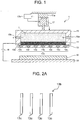
- FIG. 1 is a schematic exploded sectional view of a film forming apparatus 1 for a metal film of the embodiments of the present invention.
- FIG. 2A is a view showing a state of fibers included in a solid electrolyte membrane 13 shown in FIG. 1
- FIG. 2B and FIG. 2C show variations of the fibers shown in FIG. 2A .
- the film forming apparatus 1 according to the present embodiment is an apparatus forming a metal film on a surface of a substrate W.
- the substrate W may be formed by an aluminum (aluminum or aluminum alloy)-base material, a copper (copper or copper alloy)-base material, or a nickel (nickel or nickel alloy)-base material; and alternatively, the substrate W may be a substrate including a surface layer of one of the above metals formed on a surface of a non-conductive substrate, such as a silicon substrate and a resin substrate.
- a non-conductive substrate such as a silicon substrate and a resin substrate.
- the film forming apparatus 1 includes an anode 11, the solid electrolyte membrane 13 disposed between the anode 11 and the substrate W serving as a cathode, and a solution storage part 15 storing a metallic solution L containing metallic ions such that the metallic solution L comes in contact with the solid electrolyte membrane 13 from the anode 11 side. Furthermore, the film forming apparatus 1 includes a pressing part 17 pressing the solid electrolyte membrane 13 onto the substrate W, an electric power source 18 applying voltage between the anode 11 and the substrate W, and a placement table 19 on which the substrate W is placed.
- the placement table 19 is made of a metallic material, and electrically connects the substrate W and the electric power source 18 via the placement table 19.
- the placement table 19 may be omitted as far as the substrate W can stably be pressed by the solid electrolyte membrane 13, and the substrate W can be electrically connected to the electric power source 18.
- the anode 11 As an example of the anode 11, ruthenium oxide, platinum, or iridium oxide, which are insoluble in the metallic solution L, can be listed; and the anode 11 may be an anode formed by a copper plate coated with one of these metals. In the present embodiment, the anode 11 may be a soluble anode formed by the same metal (metal of metallic ions in the metallic solution L) as the metal of the metal film, and for example, if the metal film is a nickel film, the anode 11 is formed by nickel.
- the anode 11 is made of a porous material that the metallic solution L permeates and supplies the metallic ions to the solid electrolyte membrane.
- the porous material is not limited to a specific one, and any material may be employed as far as the porous material (1) has a corrosion resistance against the metallic solution L, (2) has enough electric conductivity for acting as an anode, (3) allows the metallic solution L to permeate the porous material, and (4) can be pressurized by the pressing part 17 described later; and for example, as an example of the above porous material, a metallic foamed body, such as titanium foam, having a smaller ionization tendency (or having a higher electrode potential) than that of plated metallic ions, and the metallic foamed body is formed by continuous foamed body having open pores.
- the porous body is used for the anode 11, but the anode 11 may be made of a non-porous body as far as a space can be provided between the solid electrolyte membrane 13 and the anode 11, and the metallic solution L can be stored in this space.
- the solid electrolyte membrane 13 can soak up the metallic ions thereinside when being in contact with the metallic solution L as described above, and can precipitate a metal deriving from the metallic ions on the surface of the substrate W when the voltage is applied by the electric power source 18. Detailed description of the configuration of the solid electrolyte membrane 13 will be provided later.
- the solution storage part 15 stores the metallic solution L such that the metallic solution L is in contact with the solid electrolyte membrane 13 on the anode 11 side.
- the solution storage part 15 is sealed by the solid electrolyte membrane 13 from the side where the substrate W is disposed.
- the anode 11 is a porous body; therefore, if the solution storage part 15 on the anode 11 side is charged with the metallic solution L while the anode 11 and the solid electrolyte membrane 13 are stacked, the metallic solution L permeates the anode 11, and the metallic solution L having permeated the anode 11 comes in contact with the solid electrolyte membrane 13 from the anode 11 side.
- the solution storage part 15 is formed with a supply passage 15a supplying the metallic solution L, and a discharge passage 15b discharging this metallic solution.
- the solution storage part 15 is made of an insoluble material to the metallic solution L, and may be formed by either of metal and resin.
- An example of the metallic solution L may include an electrolyte containing ions of copper, nickel, silver, or the like, the composition of the metallic solution L is not limited to a specific one as far as the metal to be the metal film can stay in an ionic state.
- An example of a solvent of the metallic solution L may include water, alcohol, or the like.
- an example of the solvent of the metallic solution L may include nickel sulfate, nickel nitrate, nickel acetate, or the like.
- the solution storage part 15 is connected to a supply source (not illustrated) supplying the metallic solution L, and the metallic solution L supplied from the supply source is supplied via the supply passage 15a into the inside of the solution storage part 15, and is then discharged from the discharge passage 15b to the outside of the solution storage part 15.
- a supply source not illustrated
- the pressing part 17 is a device configured to be connected to the solution storage part 15, and to press the solid electrolyte membrane 13 onto the substrate W.
- a mechanism of the pressing part 17 is not limited to a specific one as far as the solid electrolyte membrane 13 can be pressed onto the substrate W by moving the solution storage part 15 toward the substrate W.
- an electric actuator of a direct driven type configured to move the solution storage part 15 toward the substrate W is exemplified, but a cylinder of a hydraulic type or a pneumatic type that moves the solution storage part 15 toward the substrate W may also be employed.
- the film forming apparatus 1 may further include, if necessary, a pressure measurement unit 17a like a load cell configured to measure a pressure pressed by the pressing part 17, and a controller 17b configured to control the pressure by the pressing part 17 such that the pressure measured by the pressure measurement unit 17a becomes constant.
- a pressure measurement unit 17a like a load cell configured to measure a pressure pressed by the pressing part 17
- a controller 17b configured to control the pressure by the pressing part 17 such that the pressure measured by the pressure measurement unit 17a becomes constant.
- the pressing part 17 is an electric actuator of a direct driven type
- the controller 17b controls current to be supplied to the actuator of a direct driven type.
- the controller 17b controls pressure of a working fluid to be supplied to the pressing part 17.
- the electric power source 18 is a DC power source to apply voltage between the anode 11 and the substrate W, but the electric power source 18 may be an AC power source as far as the electric power source can apply voltage between the anode 11 and the substrate W.
- a positive electrode of the electric power source 18 is connected to the anode 11, and a negative electrode of the electric power source 18 is connected to the placement table 19.
- the placement table 19 is electrically connected to the substrate W, as described later.
- the substrate W serves as a cathode.
- the solid electrolyte membrane 13 includes: a first portion 13a formed by an ion permeable material that the metallic ions permeate; and a second portion 13b formed by a material having an electric insulating property and having a lower permeability of the metallic ions than that of the ion permeable material of the first portion 13a.
- the "material having a lower permeability of the metallic ions" referred to in the present specification also includes a "material that no metallic ions permeate".
- the material of the first portion 13a is not limited to a specific one as far as the material is an ion permeable material that the metallic solution permeates, and for example, as the material of the first portion 13a, fluorine-based resins such as Nafion (R) manufactured by DuPont, Inc., carbohydrate-based resins, polyamic acid resins, and solid electrolyte (resin) having a cation exchange function such as Selemion (CMV, CMD, CMF series) manufactured by Asahi Glass Co., Ltd, and others may be listed.
- a film thickness of the solid electrolyte membrane 13 may be 100 to 300 ⁇ m.
- the material of the second portion 13b is not limited to a specific one as far as the material has an electric insulating property, and also has a lower permeability of the metallic ions than that of the ion permeable material of the first portion 13a; and this material is formed by a dielectric substance to be polarized when voltage is applied by the electric power source 18, such as nylon 66, MC nylon, polytetrafluoroethylene (PTFE), vinyl chloride, and others.
- the present inventor has measured mechanical characteristics of the above-exemplified materials of the first portion 13a and the above-exemplified materials of the second portion 13b; and they were both made of resin materials, and thus they had almost the same mechanical characteristics. Accordingly, during the film formation as described later, when the solid electrolyte membrane 13 was pressed onto the substrate W, the second portion was not separated from the first portion 13a.
- the first portion 13a is formed by a fluorine-based resin
- the second portion 13b is formed by a fluorine-based resin such as polytetrafluoroethylene (PTFE)
- PTFE polytetrafluoroethylene
- the second portion 13b is embedded in the first portion 13a in such a manner that the second portion 13b is exposed from the surface of the solid electrolyte membrane 13, the surface facing the substrate W.
- the second portion 13b is embedded in the solid electrolyte membrane 13 only on the substrate W side.
- the second portion 13b is formed such that when voltage is applied between the anode 11 and the substrate W by the electric power source 18, the metallic ions passing through the first portion 13a pass around the second portion 13b, and the metal of the metallic ions is then precipitated on the surface of the substrate W, the surface facing the second portion 13b.
- the above-configured second portion 13b can be obtained by appropriately selecting a shape and a dimension of the second portion 13b, a ratio of the second portion 13b contained in the solid electrolyte membrane 13, and others under the above-described conditions of the material of the second portion 13b, in such a manner that when voltage is applied, the metal of the metallic ions is precipitated on the surface of the substrate W, the surface facing the second portion 13b.
- Such a second portion 13b may be configured by multiple blocks, multiple wires, multiple particles, or multiple fibers; and the multiple fibers may be either of long fibers and short fibers.
- the second portion 13b is formed by fibers 13c extending in one direction (that is, aligned in line in one direction) with intervals between the fibers as shown in FIG.2A .
- the dimension and the number of the fibers 13c are schematically illustrated, and for example, it is preferable to align approximately 1.6 to 16 fibers 13c per 1cm.
- the second portion 13b may be formed by plain fabric woven by multiple warps (fibers) 13d and multiple woofs (fibers) 13e, as shown in FIG. 2B ; and fabric other than this, such as twill fabric and satin fabric, may also be employed.
- the second portion 13b may be formed by leno weave fabric (cross weave fabric) structured by twisting warps (fibers) 13f and sacrifice yarns (fibers) 13g around woofs (fibers) 13h. In each of the warps (fibers) 13f and the woofs (fibers) 13h, it is preferable to align approximately 1.6 to 16 fibers per 1cm. As shown in FIG. 2B and FIG. 2C , if the second portion 13b is fabric formed by multiple fibers, it is possible to increase strength of the solid electrolyte membrane 13.
- Each of the multiple fibers shown in FIG. 2A to FIG. 2C has an oval sectional shape, and as shown in FIG. 1 , because of this shape, each of these fibers included in the second portion 13b has a portion swelling toward the side where the substrate W is disposed.
- each fiber has such a swelling portion
- the sectional shape of each fiber may be any shape, such as a circular shape and a polygonal shape, and the sectional shape thereof is not limited to a specific one.
- a fiber diameter of each fiber may be within a range of 12 to 70 ⁇ m.
- An aspect ratio of each fiber may be within a range of 1 to 10 or 1 to 3.
- the aspect ratio is a ratio between a width of a longer axis of the section (maximum width of the section) and a width of a shorter axis orthogonal to the longer axis; and an aspect ratio of a circle is 1.
- FIG. 3 is a variation of the film forming apparatus shown in FIG. 1 .
- This film forming apparatus is different from the film forming apparatus shown in FIG. 1 in that solid electrolyte membranes are stacked.
- the other configurations are the same, and thus detailed description thereof will be omitted.
- the solid electrolyte membrane 13 of the film forming apparatus 1 shown in FIG. 1 is defined to be a first solid electrolyte membrane 13A, and a second solid electrolyte membrane 13B, formed by the same ion permeable material as that of the first portion 13a, is stacked on the first solid electrolyte membrane 13A on the side where the second solid electrolyte membrane 13B comes in contact with the metallic solution L of the solution storage part 15. Specifically, the second solid electrolyte membrane 13B seals the solution storage part 15.
- this film forming apparatus 1 may be configured that when a metal film having a different film pattern is formed, the first solid electrolyte membrane 13A is removed from the second solid electrolyte membrane 13B, and then another first solid electrolyte membrane 13A for forming a metal film having a different film pattern is mounted to the second solid electrolyte membrane 13B.
- the solution storage part 15 is sealed by the second solid electrolyte membrane 13B, it is possible to prevent leakage of the metallic solution L from the solution storage part 15.
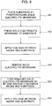
- FIG. 4 is a flowchart explaining the first film forming method using the film forming apparatus 1 shown in FIG. 1 .
- step S11 as shown in FIG. 1 , the substrate W is placed at a position facing the solid electrolyte membrane 13. With this, the solid electrolyte membrane 13 is disposed between the anode 11 and the substrate W.
- the metallic solution L is disposed in the solution storage part 15 such that the metallic solution L containing the metallic ions comes in contact with the solid electrolyte membrane 13 from the anode 11 side.
- step S12 the solid electrolyte membrane 13 is pressed onto the substrate W by the pressing part 17.
- the pressure pressed by the pressing part 17 is measured by the pressure measurement unit 17a, and the pressing of the pressing part 17 is controlled by the controller 17b so as to set the pressure measured by the pressure measurement unit 17a to be constant.
- the controller 17b controls the controller 17b so as to set the pressure measured by the pressure measurement unit 17a to be constant.
- step S13 by applying voltage between the anode 11 and the substrate W by the electric power source 18 while maintaining this pressing state, the metal film F deriving from the metallic ions is formed on the substrate W.
- the portion of the solid electrolyte membrane 13, the portion facing the second portion 13b becomes a precipitating region where the metal is precipitated
- the portion of the solid electrolyte membrane 13, the portion facing the first portion 13a becomes a non-precipitating region where the metal is unlikely to be precipitated.
- the second portion 13b is formed by the multiple fibers 13c extending in one direction, it is possible to form the metal film F with a stripe pattern, which is formed by linear metallic projections f where the metal is precipitated.
- the woofs (fibers) 13h having thicker element yarns than those of the warps (fibers) 13f and the sacrifice yarns 13g are more likely to be strongly pressed onto the substrate W, to thus form the metal film F with a stripe pattern.
- each of the linear metallic projections f (section orthogonal to the direction where the metallic projections f extend) has a triangular sectional shape, which sharply projects in a direction apart from the substrate W. Such a shape promotes an anchor effect of the surface of the substrate W on which the metal film F is formed.
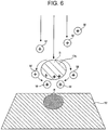
- FIG. 6 is a view explaining the film formation principle according to the present embodiment.
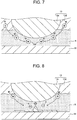
- FIG. 7 is an enlarged sectional view of the major part of FIG. 6 .
- FIG. 8 is a view explaining a growth state of the metallic projection during the film formation.
- a minimum passage of the metallic ions that pass through the solid electrolyte membrane 13 by applying voltage between the anode 11 and substrate W is a straight passage orthogonally extending from one surface to the other surface of the solid electrolyte membrane 13 (i.e. a passage extending along a direction orthogonal to the solid electrolyte membrane 13).
- the metallic ions M cannot move through the solid electrolyte membrane 13 in a straight perpendicular line, and thus the metallic ions inevitably move through passages avoiding the fibers 13c of the second portion 13b.
- Shadowing a portion of the solid electrolyte membrane 13 in which the metallic ions M inevitably move through the passages avoiding the fibers 13c is referred to as a shadow section S.
- Introducing the shadow section S into the solid electrolyte membrane 13 by using the fibers 13c of the second portion 13b encourages reduction in amount of the metallic ions M passing through the portion of the solid electrolyte membrane 13, the portion actively conveying the metallic ions M, to thereby increase operating voltage of the solid electrolyte membrane 13.
- a portion of the substrate W, the portion facing the shadow section S in the solid electrolyte membrane 13 adjacent to the substrate W in the direction where metallic ion fluxes pass through the first portion 13a, is referred to as a blind section B.
- the fibers 13c of the second portion 13b are locally disposed in the surface located on the substrate W side of the solid electrolyte membrane 13 so as to decrease the shadow section S in a thickness direction of the solid electrolyte membrane 13. It is thereby possible to suppress increase in operating voltage of the solid electrolyte membrane 13.
- the metallic ions M are soaked inside the solid electrolyte membrane 13, and the metal is precipitated from the metallic ions M to the surface of the substrate W.
- Nernst diffusion layer R A diffusion limiting current I in the Nernst diffusion layer R is in inverse proportion to a thickness of the Nernst diffusion layer R, as shown in the following formula.
- I Z ⁇ F ⁇ D ⁇ C / ⁇ , where I: diffusion limiting current, Z: valence number of metallic ions, F: Faraday constant, D: diffusion constant, C: concentration of metallic solution (electrolyte), ⁇ : Nernst diffusion layer R.
- the metallic ions M moving along an interface between the fibers 13c of the second portion 13b and the first portion are likely to be conveyed to the section where the substrate W and the fibers 13c are in contact with each other (blind section B) because a thickness of the Nernst diffusion layer R in the section where the substrate W and the fibers 13c are in contact with each other is thinner than a thickness of the Nernst diffusion layer R in the other portions.
- the Nernst diffusion layer R having the thickness in the blind section B with the fibers 13c in contact is decreased, to thereby increase the above-described diffusion limiting current; therefore, the metallic ions M are collected to the interface between the substrate W and the fibers 13c, and the metal is thereby precipitated to this portion.
- the metallic projections f having a thicker thickness than the predetermined thickness are formed on the metal film F formed by the film forming apparatus 1. This reason will be explained, hereinafter.
- Field electron emission is a phenomenon that electrons are emitted from a solid surface by externally applying an electric field to increase a tunneling probability (e.g. see O.UjsaghyPhys.rev.Lett.85,12,2558,2000).
- energy equal to the work function should be given from an electronic level until a vacuum level of the solid body, and if the energy is not more than this, the electrons are repelled against an image potential barrier.
- voltage is externally applied to form an external electric field potential, and a barrier of a synthetic potential of the external electric field potential and the image potential is thereby generated. Then, the electrons are emitted from the solid surface into vacuum with energy not more than the work function; and this phenomenon is called as the Schottky effect.
- the gradient of the external electric field potential becomes greater, and the barrier of the synthetic potential having a width with reference to the Fermi level is generated. Because electrons have wave-particle duality, there exist electrons passing through the barrier of the width due to the tunnel effect.
- the electrons having passed through the potential barrier are emitted and accelerated to the outside by the external electric field potential.
- the potential width becomes thinner, and thus the tunnel probability becomes increased.
- the metallic projections f formed on the surface of the substrate W shown in FIG. 8 are externally provided with the electric field through further film formation; thus, field electron emission becomes easier as the distance between the metallic projections f formed on the surface of the substrate W and the solid electrolyte membrane 13 is shorter. Therefore, it can be considered that due to the shadowing, the metallic ions M, moving along the interface between the fibers 13c of the second portion 13b and the solid electrolyte membrane 13, are trapped more frequently by the electrons emitted from the metallic projections f; therefore, the thickness of the metallic projections f becomes thicker than the predetermined thickness.
- the penetration probability (tunnel probability) T of the electrons is exponentially changed depending on the distance between the fibers 13c and the metallic projections f, as shown in the following Formula.
- T penetration probability of electrons
- z distance between fibers 13c and metallic projections f
- m mass of electron e
- h Planck constant / 2 ⁇
- V voltage
- E electronic energy.
- the distance z between the fibers 13c and the metallic projections f during the film formation becomes shorter; therefore, the penetration probability of the electrons becomes higher, thus encouraging the growth of the metallic projections f.
- FIG. 9 is a flowchart explaining the second film forming method using the film forming apparatus 1 shown in FIG. 3 .
- FIG. 10 is a schematic outline view explaining the metal film F formed by the second film forming method shown in FIG. 9 .
- step S21 to step S23 are the same as the respective steps in the first film forming method.
- the substrate W is placed at a position facing the first solid electrolyte membrane 13A.
- the first solid electrolyte membrane 13A is disposed between the anode 11 and the substrate W.
- the metallic solution L is set in the solution storage part 15 such that the metallic solution L containing the metallic ions comes in contact with the first solid electrolyte membrane 13A from the anode 11 side.
- step S22 the first solid electrolyte membrane 13A is pressed onto the substrate W by the pressing part 17.
- step S23 while maintaining this pressing state, voltage is applied between the anode 11 and the substrate W by the electric power source 18 so as to form the metal film F deriving from the metallic ions on the surface of the substrate.
- the second portion 13b is formed by the multiple fibers 13c extending along one direction; therefore, as shown in the left drawing of FIG. 10 , it is possible to form the metal film F with a stripe pattern configured by linear first metallic projections f1 where the metal is precipitated (first film forming step).
- step S24 after the first film forming step, the first solid electrolyte membrane 13A together with the solution storage part 15 are lifted up to remove the first solid electrolyte membrane 13A from the substrate W. Then, in step S25, with the substrate W (metal film F) facing the first solid electrolyte membrane 13A, while the position of the substrate W is retained, the first solid electrolyte membrane 13A is turned by 90°, and is mounted to the solution storage part 15. With this operation, the first solid electrolyte membrane 13A is disposed between the anode 11 and the substrate W.
- the first solid electrolyte membrane 13A is turned by 90°, but for example, the first solid electrolyte membrane 13A may not be turned, and only the substrate W may be turned by 90°.
- step S26 the solid electrolyte membrane 13 is pressed onto the substrate W, and voltage is applied between them by the electric power source 18.
- linear second metallic projections f2 where the metal is precipitated are formed along a direction intersecting the direction where the first metallic projections f1 extend; and the metal film F with a grid pattern is formed by the second metallic projections f2 and the first metallic projections f1 (second film forming step).
- step S25 because the first solid electrolyte membrane 13A is turned by 90°, the linear first metallic projections f1 and the linear second metallic projections f2 intersect each other at 90°.
- the film formation may be carried out after the solid electrolyte membrane 13 or the substrate W is turned at this desired angle.
- the metal film F with a grid pattern can be formed; therefore, it is possible to enhance the anchor effect of the surface of the substrate W.
- a support body of an electrode (positive electrode) formed by nickel for a dischargeable battery e.g. a nickel-hydrogen battery
- a solution containing nickel ions is used as the metallic solution
- an electrode emitter or collector
- a solution containing nickel ions is used as the metallic solution
- Film formation of metal films was carried out by the following method. Specifically, films were formed by a film forming apparatus having the basic configuration of the film forming apparatus shown in FIG. 3 .
- This film forming apparatus is different from the film forming apparatus shown in FIG. 3 in that an anode is a non-porous anode, and a flowing structure of the metallic solution flowing between the anode and the solid electrolyte membrane is employed.
- a nickel plate (NI-313551, dimension: 2t ⁇ 40 ⁇ 50 mm, manufactured by The Nilaco corporation) was prepared.
- an ion exchange membrane electrolyte membrane: N117, manufactured by Sigma-Aldrich
- the first solid electrolyte membrane an electrolyte membrane a: N424, and an electrolyte membrane b: N324, manufactured by Sigma-Aldrich
- the second portion formed by leno weave fabric shown in FIG. 2C and others was embedded in the first portion.
- the aspect ratio of the section of each yarn that is a fiber included in the electrolyte membrane a was within a range of 1 to 3
- the aspect ratio of the section of each yarn that is a fiber included in the electrolyte membrane b was within a range of 1.5 to 3.
- the aspect ratio is a ratio of a width of a longer axis of the section (maximum width of the section) and a width of a shorter axis orthogonal to this longer axis.
- a nickel foil film thickness: 15 ⁇ m, dimension: 1260 ⁇ 350 mm, manufactured by Fukuda Metal Foil & Powder Co., Ltd.
- the film forming condition was as follows: a temperature of the substrate was 80°C, a pressing pressure was 0.1 MPa, a film forming speed was 0.20 ⁇ m min., and a nickel film forming area was 2.5 cm ⁇ 2.5 cm.
- the film formation was carried out by the second film forming method shown in FIG. 9 .
- a metal film with a stripe pattern was formed. This can be considered that metallic projections were formed on the surface facing woofs of the leno weave fabric.
- the first solid electrolyte membrane was removed from the film forming apparatus, and then the first solid electrolyte membrane was mounted to the film forming apparatus again while the first solid electrolyte membrane is turned by 90° so as to carry out the metal film formation.
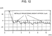
- FIG. 11 shows a photograph of a surface of the metal film formed in the confirmation test using the electrolyte membrane a. Furthermore, in order to confirm heights of the metallic projections of the metal film, a profile curve (surface roughness) was measured by a roughness meter (SURFCOM1400G25, manufactured by Tosei Systems Co., Ltd.).
- FIG. 12 is a graph showing measurement results of the surface roughness of the metal film formed in the confirmation test using the electrolyte membrane a.
- the metal film facing the second portion is also formed with metallic projections having a shape shown in FIG.11 .
Landscapes
- Chemical & Material Sciences (AREA)
- Chemical Kinetics & Catalysis (AREA)
- Engineering & Computer Science (AREA)
- Organic Chemistry (AREA)
- Materials Engineering (AREA)
- Metallurgy (AREA)
- Electrochemistry (AREA)
- Inorganic Chemistry (AREA)
- Mechanical Engineering (AREA)
- Life Sciences & Earth Sciences (AREA)
- Sustainable Development (AREA)
- Electroplating Methods And Accessories (AREA)
- Fuel Cell (AREA)
Abstract
Description
- The present invention relates to a film forming method for forming a metal film on a surface of a substrate and a film forming apparatus for the same, and particularly relates to a film forming method for forming a metal film on a surface of a substrate by applying voltage between an anode and the substrate via a solid electrolyte membrane, and a film forming apparatus for the same.
- Conventionally, when a metal film is formed on a surface of a substrate, the metal film is sometimes formed using a film forming apparatus including a solid electrolyte membrane. In such a film forming apparatus, for example, in Japanese Patent Application Publication No.
2016-169398 JP 2016-169398 A - The solid electrolyte membrane of the film forming apparatus is formed with recessed portions that are recessed relative to a contact surface in contact with a film forming region such that the solid electrolyte membrane comes in contact with the film forming region in the surface of the substrate, the region where the metal film is formed, and the solid electrolyte membrane is out of contact with the surface excluding the film forming region. With this configuration, since portions (specifically, projecting portions) excluding the recessed portions in the solid electrolyte membrane are partially in contact with the surface of the substrate, it is possible to form a metal film on a part of the surface of the substrate.
- However, when the metal film is formed using the film forming apparatus disclosed in
JP 2016-169398 A - The present invention provides a film forming method for a metal film that can form a metal film within a desired range in a substrate, and a film forming apparatus for the same.
- In light of the above problem, the inventors have repeatedly conducted enthusiastic studies, and have finally come to such a conclusion that by bringing the metallic ions passing through the solid electrolyte membrane to move so as to be collected to a predetermined position located on the substrate side, it is possible to form the metal film in a desired region in the substrate.
- A film forming method for a metal film according to the first aspect of the present invention, includes: supplying a metallic solution containing metallic ions such that the metallic solution comes in contact with a solid electrolyte membrane from an anode side of the solid electrolyte membrane in a state in which the solid electrolyte membrane is disposed between the anode and a substrate; pressing the solid electrolyte membrane to the substrate; and applying voltage between the anode and the substrate in a state in which the solid electrolyte membrane is pressed to the substrate so as to form a metal film deriving from the metallic ions on a surface of the substrate, wherein the solid electrolyte membrane includes: a first portion made of an ion permeable material that the metallic ions permeate; and a second portion made of a material having an electric insulating property and having a lower permeability of the metallic ions than that of the ion permeable material of the first portion, the second portion being embedded in the first portion so as to be exposed from a surface of the solid electrolyte membrane, the surface of the solid electrolyte membrane facing the substrate.
- According to the first aspect of the present invention, when the voltage is applied between the anode and the substrate in a state in which the solid electrolyte membrane is pressed onto the substrate, the second portion becomes polarized. When the metallic ions having passed through the first portion come closer to the polarized second portion, the metallic ions are attracted toward the second portion, and then move in the vicinity of the interface between the first portion and the second portion, toward the substrate. Since the metallic solution between the substrate and the second portion functions as a Nernst diffusion layer, the metallic ions move on the surface of the substrate facing the second portion, and the metal of the metallic ions is precipitated thereon. Due to the tunnel effect, the metallic ions move in such a manner as to be collected on the surface of the substrate facing the second portion, the metal film is unlikely to be formed on the surface of the substrate facing the first portion. Accordingly, it is possible to form the metal film to be located within a desired range in the substrate. Note that the precipitation principle of the metal (film formation principle of the metal film) will be explained in the following description of the embodiment.
- "The solid electrolyte membrane including the second portion formed such that when the voltage is applied, the metallic ions passing through the first portion pass around the second portion, and a metal of the metallic ions is precipitated on the surface of the substrate, the surface facing the second portion" as set forth in the first aspect of the present invention, as described later, can be obtained by appropriately selecting a shape and a dimension of the second portion, a rate of the second portion included in the solid electrolyte membrane, and others, under conditions of the material of the second portion in such a manner that the metal of the metallic ions is precipitated on the surface of the substrate, the surface facing the second portion when voltage is applied.
- In the first aspect of the present invention, the solid electrolyte membrane may include the second portion formed such that when the voltage is applied, the metallic ions passing through the first portion pass around the second portion, and a metal of the metallic ions is precipitated on the surface of the substrate, the surface of the substrate facing the second portion.
- Further, in the first aspect of the present invention, the second portion may include portions swelling toward the side where the substrate is disposed. According to this aspect, because the second portion has portions swelling toward the side where the substrate is disposed, the metallic ions move around the swelling portions of the second portion, so that the metallic ions can easily move. Accordingly, it is possible to form the metal film in a finer area.
- In this case, the second portion may include multiple blocks, multiple wires, multiple particles, or multiple fibers. For example, if the second portion is formed by multiple fibers, the metallic ions move along the surface of the substrate, the surface facing the respective fibers of the multiple fibers, and the metal thereof is precipitated thereon; therefore, it is possible to form, on the surface of the substrate, the metal film with a pattern corresponding to the fiber patterns of the multiple fibers.
- In the case in which the second portion is formed by the multiple fibers, "the second portion formed such that when the voltage is applied, the metallic ions passing through the first portion pass around the second portion, and a metal of the metallic ions is precipitated on the surface of the substrate, the surface facing the second portion" set forth in the first aspect of the present invention corresponds to the "second portion formed by the multiple fibers"; and by using the multiple fibers, it is possible to precipitate the metal of the metallic ions on the surface of the substrate, facing the respective fibers.
- In the first aspect of the present invention, the second portion includes multiple fibers extending along one direction with intervals between the fibers, wherein the film forming method includes: pressing the solid electrolyte membrane to the substrate and applying voltage so as to form a metal film with a stripe pattern including linear first metallic projections where the metal is precipitated, on the surface of the substrate, the surface facing the fibers (first film forming step); after the first film forming step, turning the substrate or the solid electrolyte membrane with the metal film facing the solid electrolyte membrane; and after turning the substrate or the solid electrolyte membrane, by pressing the solid electrolyte membrane to the substrate and applying voltage, forming linear second metallic projections where the metal is precipitated, along a direction intersecting the direction where the first metallic projections extend so as to form a metal film with a grid pattern including the first metallic projections and the second metallic projections (second film forming step).
- According to this aspect, through the first film forming step and the second film forming step, the metal film with a grid pattern can be formed; therefore, it is possible to promote an anchor effect on the surface of the substrate.
- The present specification discloses a film forming apparatus for suitably carrying out the aforementioned film forming method for a metal film. The film forming apparatus for a metal film according to the second aspect of the present invention relates to a film forming apparatus for a metal film, including: an anode; a solid electrolyte membrane disposed between the anode and the substrate; a solution storage part storing a metallic solution containing metallic ions such that the metallic solution comes in contact with the solid electrolyte membrane from an anode side of the solid electrolyte membrane; a pressing part pressing the solid electrolyte membrane to the substrate; and an electric power source applying voltage between the anode and the substrate, wherein the film forming apparatus forms a metal film deriving from the metallic ions on a surface of the substrate by applying voltage by the electric power source. The solid electrolyte membrane of the second aspect of the present invention includes: a first portion made of an ion permeable material that the metallic ions permeate; and a second portion made of a material having an electric insulating property and having a lower permeability of the metallic ions than that of the ion permeable material, the second portion being embedded in the first portion so as to be exposed from a surface of the solid electrolyte membrane, the surface of the solid electrolyte membrane facing the substrate.
- According to the second aspect of the present invention, in the state in which the solid electrolyte membrane is pressed onto the substrate by the pressing part, when voltage is applied between the anode and the substrate by the electric power source, the second portion becomes polarized, and the metallic ions having passed through the first portion come closer to the polarized second portion. The metallic ions are further attracted to the second portion, and move through the vicinity of the interface between the first portion and the second portion toward the substrate. Since the metallic ions permeate the first portion, the metallic solution slightly oozes, so that the metallic solution is present between the substrate and the second portion, thus functioning as the Nernst diffusion layer. Hence, the metallic ions move to the surface of the substrate facing the second portion, and the metal of the metallic ions is precipitated thereon. In addition, due to the tunnel effect, the metallic ions move in such a manner as to be collected on the surface of the substrate facing the second portion, the metal film is unlikely to be formed on the surface of the substrate facing the first portion. Accordingly, it is possible to form the metal film so as to be located within a desired range in the substrate. The precipitation principle of this metal (film formation principle of the metal film) will be explained in detail in the following description of the embodiment.
- In the second aspect of the present invention, the second portion may be formed such that when the voltage is applied, the metallic ions passing through the first portion pass around the second portion, and a metal of the metallic ions is precipitated on the surface of the substrate, the surface of the substrate facing the second portion.
- In the second aspect of the present invention, the surface from which the second portion is exposed may include portions swelling toward a side where the substrate is disposed. According to this aspect, because the second portion has the portions swelling toward the side where the substrate is disposed, the metallic ions move around the swelling portion of the second portion, so that the metallic ions can easily move. Accordingly, it is possible to form the metal film in a finer area.
- Here, the second portion may include, for example, multiple blocks, multiple wires, multiple particles, or multiple fibers. For example, if the second portion is formed by multiple fibers, the metallic ions move to the surface of the substrate, the surface facing the respective fibers of the multiple fibers, and the metal of the metallic ions is precipitated on the surface; therefore, it is possible to form, on the surface of the substrate, the metal film with a pattern corresponding to the fiber patterns of the multiple fibers.
- In the case in which the second portion is formed by the multiple fibers, "the second portion formed such that when the voltage is applied, the metallic ions passing through the first portion pass around the second portion, and a metal of the metallic ions is precipitated on the surface of the substrate, the surface facing the second portion" in the second aspect of the present invention corresponds to the "second portion formed by the multiple fibers"; and by using the multiple fibers, it is possible to precipitate the metal of the metallic ions on the surface of the substrate facing the respective fibers.
- In the second aspect of the present invention, the second portion may include multiple fibers extending along one direction with intervals between the fibers. According to this aspect, by pressing the solid electrolyte membrane to the substrate and applying voltage, a metal film with a stripe pattern configured by linear metallic projections where the metal is precipitated can be formed on the surface of the substrate, the surface facing the respective fibers. Furthermore, after the solid electrolyte membrane is removed from the substrate, in the state in which the metal film faces the solid electrolyte membrane, the substrate or the solid electrolyte membrane is turned by a predetermined turning angle (e.g. 90°), and thereafter, the solid electrolyte membrane is pressed to the substrate and voltage is applied, to thereby form a metal film with a grid pattern formed by the linear metallic projections and newly-formed linear metallic projections.
- In addition, in the second aspect of the present invention, the solid electrolyte membrane may be set to be a first solid electrolyte membrane, and a second solid electrolyte membrane made of an ion permeable material that the metallic ions permeate may be stacked on the first solid electrolyte membrane on the side where the second solid electrolyte membrane comes in contact with the metallic solution in the solution storage part. According to this aspect, when a metal film having different film formation patterns is formed, simply by removing the first solid electrolyte membrane from the second solid electrolyte membrane, and replacing this with a different first solid electrolyte membrane, because the solution storing part is sealed by the second solid electrolyte membrane, it is possible to prevent leakage of the metallic solution from the solution storing part.
- According to the present invention, it is possible to form the metal film located within a desired range of the substrate.
- Features, advantages, and technical and industrial significance of exemplary embodiments of the invention will be described below with reference to the accompanying drawings, in which like numerals denote like elements, and wherein:
-
FIG. 1 is a schematic exploded sectional view of a film forming apparatus for a metal film of embodiments of the present invention; -
FIG. 2A is a view showing a state of fibers included in a solid electrolyte membrane shown inFIG. 1 ; -
FIG. 2B is a view showing a variation of fibers shown inFIG. 2A ; -
FIG. 2C is a view showing another variation of the fibers shown inFIG. 2A ; -
FIG. 3 is a variation of the film forming apparatus shown inFIG. 1 ; -
FIG. 4 is a flowchart explaining a first film forming method using the film forming apparatus shown inFIG. 1 ; -
FIG. 5 is a schematic sectional view explaining a film formation state of a surface of a substrate; -
FIG. 6 is a view explaining a film formation principle according to the present embodiment; -
FIG. 7 is an enlarged sectional view of a major part ofFIG. 6 ; -
FIG. 8 is a view explaining a growth state of a metallic projection during the film formation; -
FIG. 9 is a flowchart explaining a second film forming method using the film forming apparatus shown inFIG. 3 ; -
FIG. 10 is a schematic outline view explaining a metal film formed in the second film forming method shown inFIG. 9 ; -
FIG. 11 is a view showing a photograph of a surface of a metal film formed in a confirmation test; and -
FIG. 12 is a graph showing measurement results of a surface roughness of the metal film formed in the confirmation test. - Hereinafter, a film forming apparatus that can suitably carry out film formation of a metal film according to embodiments of the present invention will be described with reference to
FIG. 1 to FIG. 3 . -
FIG. 1 is a schematic exploded sectional view of afilm forming apparatus 1 for a metal film of the embodiments of the present invention.FIG. 2A is a view showing a state of fibers included in asolid electrolyte membrane 13 shown inFIG. 1 , andFIG. 2B andFIG. 2C show variations of the fibers shown inFIG. 2A . Thefilm forming apparatus 1 according to the present embodiment is an apparatus forming a metal film on a surface of a substrate W. - The substrate W may be formed by an aluminum (aluminum or aluminum alloy)-base material, a copper (copper or copper alloy)-base material, or a nickel (nickel or nickel alloy)-base material; and alternatively, the substrate W may be a substrate including a surface layer of one of the above metals formed on a surface of a non-conductive substrate, such as a silicon substrate and a resin substrate.
- The
film forming apparatus 1 includes ananode 11, thesolid electrolyte membrane 13 disposed between theanode 11 and the substrate W serving as a cathode, and asolution storage part 15 storing a metallic solution L containing metallic ions such that the metallic solution L comes in contact with thesolid electrolyte membrane 13 from theanode 11 side. Furthermore, thefilm forming apparatus 1 includes apressing part 17 pressing thesolid electrolyte membrane 13 onto the substrate W, anelectric power source 18 applying voltage between theanode 11 and the substrate W, and a placement table 19 on which the substrate W is placed. - The placement table 19 is made of a metallic material, and electrically connects the substrate W and the
electric power source 18 via the placement table 19. In the present embodiment, although thefilm forming apparatus 1 includes the placement table 19, the placement table 19 may be omitted as far as the substrate W can stably be pressed by thesolid electrolyte membrane 13, and the substrate W can be electrically connected to theelectric power source 18. - As an example of the
anode 11, ruthenium oxide, platinum, or iridium oxide, which are insoluble in the metallic solution L, can be listed; and theanode 11 may be an anode formed by a copper plate coated with one of these metals. In the present embodiment, theanode 11 may be a soluble anode formed by the same metal (metal of metallic ions in the metallic solution L) as the metal of the metal film, and for example, if the metal film is a nickel film, theanode 11 is formed by nickel. - In the present embodiment, the
anode 11 is made of a porous material that the metallic solution L permeates and supplies the metallic ions to the solid electrolyte membrane. The porous material is not limited to a specific one, and any material may be employed as far as the porous material (1) has a corrosion resistance against the metallic solution L, (2) has enough electric conductivity for acting as an anode, (3) allows the metallic solution L to permeate the porous material, and (4) can be pressurized by thepressing part 17 described later; and for example, as an example of the above porous material, a metallic foamed body, such as titanium foam, having a smaller ionization tendency (or having a higher electrode potential) than that of plated metallic ions, and the metallic foamed body is formed by continuous foamed body having open pores. - In the present embodiment, the porous body is used for the
anode 11, but theanode 11 may be made of a non-porous body as far as a space can be provided between thesolid electrolyte membrane 13 and theanode 11, and the metallic solution L can be stored in this space. - The
solid electrolyte membrane 13 can soak up the metallic ions thereinside when being in contact with the metallic solution L as described above, and can precipitate a metal deriving from the metallic ions on the surface of the substrate W when the voltage is applied by theelectric power source 18. Detailed description of the configuration of thesolid electrolyte membrane 13 will be provided later. - The
solution storage part 15 stores the metallic solution L such that the metallic solution L is in contact with thesolid electrolyte membrane 13 on theanode 11 side. Thesolution storage part 15 is sealed by thesolid electrolyte membrane 13 from the side where the substrate W is disposed. In the present embodiment, theanode 11 is a porous body; therefore, if thesolution storage part 15 on theanode 11 side is charged with the metallic solution L while theanode 11 and thesolid electrolyte membrane 13 are stacked, the metallic solution L permeates theanode 11, and the metallic solution L having permeated theanode 11 comes in contact with thesolid electrolyte membrane 13 from theanode 11 side. - The
solution storage part 15 is formed with asupply passage 15a supplying the metallic solution L, and adischarge passage 15b discharging this metallic solution. Thesolution storage part 15 is made of an insoluble material to the metallic solution L, and may be formed by either of metal and resin. - An example of the metallic solution L may include an electrolyte containing ions of copper, nickel, silver, or the like, the composition of the metallic solution L is not limited to a specific one as far as the metal to be the metal film can stay in an ionic state. An example of a solvent of the metallic solution L may include water, alcohol, or the like. For example, in the case of nickel ions, an example of the solvent of the metallic solution L may include nickel sulfate, nickel nitrate, nickel acetate, or the like.
- The
solution storage part 15 is connected to a supply source (not illustrated) supplying the metallic solution L, and the metallic solution L supplied from the supply source is supplied via thesupply passage 15a into the inside of thesolution storage part 15, and is then discharged from thedischarge passage 15b to the outside of thesolution storage part 15. - The
pressing part 17 is a device configured to be connected to thesolution storage part 15, and to press thesolid electrolyte membrane 13 onto the substrate W. A mechanism of thepressing part 17 is not limited to a specific one as far as thesolid electrolyte membrane 13 can be pressed onto the substrate W by moving thesolution storage part 15 toward the substrate W. For example, as an example of thepressing part 17, an electric actuator of a direct driven type configured to move thesolution storage part 15 toward the substrate W is exemplified, but a cylinder of a hydraulic type or a pneumatic type that moves thesolution storage part 15 toward the substrate W may also be employed. - In addition, in the present embodiment, the
film forming apparatus 1 may further include, if necessary, apressure measurement unit 17a like a load cell configured to measure a pressure pressed by thepressing part 17, and acontroller 17b configured to control the pressure by thepressing part 17 such that the pressure measured by thepressure measurement unit 17a becomes constant. Although not illustrated in detail inFIG. 1 , if thepressing part 17 is an electric actuator of a direct driven type, thecontroller 17b controls current to be supplied to the actuator of a direct driven type. If thepressing part 17 is a cylinder of a hydraulic type or a pneumatic type, thecontroller 17b controls pressure of a working fluid to be supplied to thepressing part 17. - In the present embodiment, the
electric power source 18 is a DC power source to apply voltage between theanode 11 and the substrate W, but theelectric power source 18 may be an AC power source as far as the electric power source can apply voltage between theanode 11 and the substrate W. A positive electrode of theelectric power source 18 is connected to theanode 11, and a negative electrode of theelectric power source 18 is connected to the placement table 19. The placement table 19 is electrically connected to the substrate W, as described later. Hence, the substrate W serves as a cathode. - In the present embodiment, the
solid electrolyte membrane 13 includes: afirst portion 13a formed by an ion permeable material that the metallic ions permeate; and asecond portion 13b formed by a material having an electric insulating property and having a lower permeability of the metallic ions than that of the ion permeable material of thefirst portion 13a. The "material having a lower permeability of the metallic ions" referred to in the present specification also includes a "material that no metallic ions permeate". - The material of the
first portion 13a is not limited to a specific one as far as the material is an ion permeable material that the metallic solution permeates, and for example, as the material of thefirst portion 13a, fluorine-based resins such as Nafion (R) manufactured by DuPont, Inc., carbohydrate-based resins, polyamic acid resins, and solid electrolyte (resin) having a cation exchange function such as Selemion (CMV, CMD, CMF series) manufactured by Asahi Glass Co., Ltd, and others may be listed. A film thickness of thesolid electrolyte membrane 13 may be 100 to 300 µm. - The material of the
second portion 13b is not limited to a specific one as far as the material has an electric insulating property, and also has a lower permeability of the metallic ions than that of the ion permeable material of thefirst portion 13a; and this material is formed by a dielectric substance to be polarized when voltage is applied by theelectric power source 18, such as nylon 66, MC nylon, polytetrafluoroethylene (PTFE), vinyl chloride, and others. - The present inventor has measured mechanical characteristics of the above-exemplified materials of the
first portion 13a and the above-exemplified materials of thesecond portion 13b; and they were both made of resin materials, and thus they had almost the same mechanical characteristics. Accordingly, during the film formation as described later, when thesolid electrolyte membrane 13 was pressed onto the substrate W, the second portion was not separated from thefirst portion 13a. In particular, if thefirst portion 13a is formed by a fluorine-based resin, and thesecond portion 13b is formed by a fluorine-based resin such as polytetrafluoroethylene (PTFE), it is possible to promote enhancement of a tight contact between them. - In this case, the
second portion 13b is embedded in thefirst portion 13a in such a manner that thesecond portion 13b is exposed from the surface of thesolid electrolyte membrane 13, the surface facing the substrate W. In the present embodiment, thesecond portion 13b is embedded in thesolid electrolyte membrane 13 only on the substrate W side. Thesecond portion 13b is formed such that when voltage is applied between theanode 11 and the substrate W by theelectric power source 18, the metallic ions passing through thefirst portion 13a pass around thesecond portion 13b, and the metal of the metallic ions is then precipitated on the surface of the substrate W, the surface facing thesecond portion 13b. - The above-configured
second portion 13b can be obtained by appropriately selecting a shape and a dimension of thesecond portion 13b, a ratio of thesecond portion 13b contained in thesolid electrolyte membrane 13, and others under the above-described conditions of the material of thesecond portion 13b, in such a manner that when voltage is applied, the metal of the metallic ions is precipitated on the surface of the substrate W, the surface facing thesecond portion 13b. - Such a
second portion 13b may be configured by multiple blocks, multiple wires, multiple particles, or multiple fibers; and the multiple fibers may be either of long fibers and short fibers. In the present embodiment, thesecond portion 13b is formed byfibers 13c extending in one direction (that is, aligned in line in one direction) with intervals between the fibers as shown inFIG.2A . InFIG. 1 andFIG. 3 , the dimension and the number of thefibers 13c are schematically illustrated, and for example, it is preferable to align approximately 1.6 to 16fibers 13c per 1cm. - As another aspect, the
second portion 13b may be formed by plain fabric woven by multiple warps (fibers) 13d and multiple woofs (fibers) 13e, as shown inFIG. 2B ; and fabric other than this, such as twill fabric and satin fabric, may also be employed. - Other than the above fabric, as shown in
FIG. 2C , thesecond portion 13b may be formed by leno weave fabric (cross weave fabric) structured by twisting warps (fibers) 13f and sacrifice yarns (fibers) 13g around woofs (fibers) 13h. In each of the warps (fibers) 13f and the woofs (fibers) 13h, it is preferable to align approximately 1.6 to 16 fibers per 1cm. As shown inFIG. 2B andFIG. 2C , if thesecond portion 13b is fabric formed by multiple fibers, it is possible to increase strength of thesolid electrolyte membrane 13. - Each of the multiple fibers shown in
FIG. 2A to FIG. 2C has an oval sectional shape, and as shown inFIG. 1 , because of this shape, each of these fibers included in thesecond portion 13b has a portion swelling toward the side where the substrate W is disposed. - With this configuration, as shown in
FIG. 6 described later, during the film formation, the metallic ions move around the swelling portions of the fibers of thesecond portion 13b, so that the metallic ions can easily move. Accordingly, it is possible to form the metal film in a finer area. As far as each fiber has such a swelling portion, the sectional shape of each fiber may be any shape, such as a circular shape and a polygonal shape, and the sectional shape thereof is not limited to a specific one. - A fiber diameter of each fiber may be within a range of 12 to 70 µm. An aspect ratio of each fiber may be within a range of 1 to 10 or 1 to 3. The aspect ratio is a ratio between a width of a longer axis of the section (maximum width of the section) and a width of a shorter axis orthogonal to the longer axis; and an aspect ratio of a circle is 1. By satisfying these ranges, the metallic ions passing through the
first portion 13a of thesolid electrolyte membrane 13 are likely to pass around the fibers, and be easily collected at the swelling portions of the respective fibers. -
FIG. 3 is a variation of the film forming apparatus shown inFIG. 1 . This film forming apparatus is different from the film forming apparatus shown inFIG. 1 in that solid electrolyte membranes are stacked. The other configurations are the same, and thus detailed description thereof will be omitted. - As shown in
FIG. 3 , in the present embodiment, thesolid electrolyte membrane 13 of thefilm forming apparatus 1 shown inFIG. 1 is defined to be a firstsolid electrolyte membrane 13A, and a secondsolid electrolyte membrane 13B, formed by the same ion permeable material as that of thefirst portion 13a, is stacked on the firstsolid electrolyte membrane 13A on the side where the secondsolid electrolyte membrane 13B comes in contact with the metallic solution L of thesolution storage part 15. Specifically, the secondsolid electrolyte membrane 13B seals thesolution storage part 15. - According to this
film forming apparatus 1, it may be configured that when a metal film having a different film pattern is formed, the firstsolid electrolyte membrane 13A is removed from the secondsolid electrolyte membrane 13B, and then another firstsolid electrolyte membrane 13A for forming a metal film having a different film pattern is mounted to the secondsolid electrolyte membrane 13B. In the present embodiment, since thesolution storage part 15 is sealed by the secondsolid electrolyte membrane 13B, it is possible to prevent leakage of the metallic solution L from thesolution storage part 15. - A first film forming method for the metal film according to the embodiments will be described, hereinafter.
FIG. 4 is a flowchart explaining the first film forming method using thefilm forming apparatus 1 shown inFIG. 1 . First, in step S11, as shown inFIG. 1 , the substrate W is placed at a position facing thesolid electrolyte membrane 13. With this, thesolid electrolyte membrane 13 is disposed between theanode 11 and the substrate W. In thefilm forming apparatus 1 shown inFIG. 1 , with the above-described structure, the metallic solution L is disposed in thesolution storage part 15 such that the metallic solution L containing the metallic ions comes in contact with thesolid electrolyte membrane 13 from theanode 11 side. - Next, in step S12, the
solid electrolyte membrane 13 is pressed onto the substrate W by thepressing part 17. During this pressing, it is possible that the pressure pressed by thepressing part 17 is measured by thepressure measurement unit 17a, and the pressing of thepressing part 17 is controlled by thecontroller 17b so as to set the pressure measured by thepressure measurement unit 17a to be constant. Through this control, it is possible to press thesolid electrolyte membrane 13 onto the substrate W in a stable manner, to thereby form a homogeneous metal film F. - Subsequently, in step S13, by applying voltage between the
anode 11 and the substrate W by theelectric power source 18 while maintaining this pressing state, the metal film F deriving from the metallic ions is formed on the substrate W. With this film formation, as shown inFIG. 5 , the portion of thesolid electrolyte membrane 13, the portion facing thesecond portion 13b, becomes a precipitating region where the metal is precipitated, and the portion of thesolid electrolyte membrane 13, the portion facing thefirst portion 13a, becomes a non-precipitating region where the metal is unlikely to be precipitated. Because thesecond portion 13b is formed by themultiple fibers 13c extending in one direction, it is possible to form the metal film F with a stripe pattern, which is formed by linear metallic projections f where the metal is precipitated. - For example, as shown in
FIG. 2C , if leno weave fabric is used for thesecond portion 13b, according to the experiments conducted by the inventors described later, the woofs (fibers) 13h having thicker element yarns than those of the warps (fibers) 13f and thesacrifice yarns 13g are more likely to be strongly pressed onto the substrate W, to thus form the metal film F with a stripe pattern. - In addition, the section of each of the linear metallic projections f (section orthogonal to the direction where the metallic projections f extend) has a triangular sectional shape, which sharply projects in a direction apart from the substrate W. Such a shape promotes an anchor effect of the surface of the substrate W on which the metal film F is formed.
- Here, with reference to
FIG. 6 to FIG. 8 , the film formation principle of the above-described metal film F will be described.FIG. 6 is a view explaining the film formation principle according to the present embodiment.FIG. 7 is an enlarged sectional view of the major part ofFIG. 6 .FIG. 8 is a view explaining a growth state of the metallic projection during the film formation. - Normally, a minimum passage of the metallic ions that pass through the
solid electrolyte membrane 13 by applying voltage between theanode 11 and substrate W is a straight passage orthogonally extending from one surface to the other surface of the solid electrolyte membrane 13 (i.e. a passage extending along a direction orthogonal to the solid electrolyte membrane 13). - However, in the
second portion 13b of thesolid electrolyte membrane 13 used in the present embodiment, the metallic ions M cannot move through thesolid electrolyte membrane 13 in a straight perpendicular line, and thus the metallic ions inevitably move through passages avoiding thefibers 13c of thesecond portion 13b. - This phenomenon is referred to as shadowing, and a portion of the
solid electrolyte membrane 13 in which the metallic ions M inevitably move through the passages avoiding thefibers 13c is referred to as a shadow section S. Introducing the shadow section S into thesolid electrolyte membrane 13 by using thefibers 13c of thesecond portion 13b encourages reduction in amount of the metallic ions M passing through the portion of thesolid electrolyte membrane 13, the portion actively conveying the metallic ions M, to thereby increase operating voltage of thesolid electrolyte membrane 13. - Here, a portion of the substrate W, the portion facing the shadow section S in the
solid electrolyte membrane 13 adjacent to the substrate W in the direction where metallic ion fluxes pass through thefirst portion 13a, is referred to as a blind section B. In thesolid electrolyte membrane 13 of the present embodiment, thefibers 13c of thesecond portion 13b are locally disposed in the surface located on the substrate W side of thesolid electrolyte membrane 13 so as to decrease the shadow section S in a thickness direction of thesolid electrolyte membrane 13. It is thereby possible to suppress increase in operating voltage of thesolid electrolyte membrane 13. - During the film formation, by applying voltage between the
anode 11 and the substrate W, the metallic ions M are soaked inside thesolid electrolyte membrane 13, and the metal is precipitated from the metallic ions M to the surface of the substrate W. - At this time, in the section where the substrate W and the
fibers 13c of thesecond portion 13b are in contact with each other (i.e. the blind section B) as well as the vicinity of this region, a slight amount of the metallic solution L having permeated thesolid electrolyte membrane 13 is formed as a Nernst diffusion layer R (seeFIG. 7 ). A diffusion limiting current I in the Nernst diffusion layer R is in inverse proportion to a thickness of the Nernst diffusion layer R, as shown in the following formula.

- Specifically, due to the shadowing, the metallic ions M moving along an interface between the
fibers 13c of thesecond portion 13b and the first portion are likely to be conveyed to the section where the substrate W and thefibers 13c are in contact with each other (blind section B) because a thickness of the Nernst diffusion layer R in the section where the substrate W and thefibers 13c are in contact with each other is thinner than a thickness of the Nernst diffusion layer R in the other portions. - Specifically, due to the pressurizing onto the substrate W by the
solid electrolyte membrane 13, the Nernst diffusion layer R having the thickness in the blind section B with thefibers 13c in contact is decreased, to thereby increase the above-described diffusion limiting current; therefore, the metallic ions M are collected to the interface between the substrate W and thefibers 13c, and the metal is thereby precipitated to this portion. - In addition, when the metal film is formed under a condition to form a smooth metal film having a predetermined thickness, the metallic projections f having a thicker thickness than the predetermined thickness are formed on the metal film F formed by the
film forming apparatus 1. This reason will be explained, hereinafter. - Field electron emission is a phenomenon that electrons are emitted from a solid surface by externally applying an electric field to increase a tunneling probability (e.g. see O.UjsaghyPhys.rev.Lett.85,12,2558,2000). In order to emit electrons from the solid surface to the outside, energy equal to the work function should be given from an electronic level until a vacuum level of the solid body, and if the energy is not more than this, the electrons are repelled against an image potential barrier. When voltage is externally applied to form an external electric field potential, and a barrier of a synthetic potential of the external electric field potential and the image potential is thereby generated. Then, the electrons are emitted from the solid surface into vacuum with energy not more than the work function; and this phenomenon is called as the Schottky effect.
- As the externally applied voltage is gradually increased, the gradient of the external electric field potential becomes greater, and the barrier of the synthetic potential having a width with reference to the Fermi level is generated. Because electrons have wave-particle duality, there exist electrons passing through the barrier of the width due to the tunnel effect.
- The electrons having passed through the potential barrier are emitted and accelerated to the outside by the external electric field potential. At this time, by gradually increasing the voltage externally applied, the potential width becomes thinner, and thus the tunnel probability becomes increased. By forming the solid body in a recess-projection shape, it is possible to generate a non-uniform electric field so as to increase the tunnel probability from the surface.
- With the above tunnel effect, the metallic projections f formed on the surface of the substrate W shown in
FIG. 8 are externally provided with the electric field through further film formation; thus, field electron emission becomes easier as the distance between the metallic projections f formed on the surface of the substrate W and thesolid electrolyte membrane 13 is shorter. Therefore, it can be considered that due to the shadowing, the metallic ions M, moving along the interface between thefibers 13c of thesecond portion 13b and thesolid electrolyte membrane 13, are trapped more frequently by the electrons emitted from the metallic projections f; therefore, the thickness of the metallic projections f becomes thicker than the predetermined thickness. - That is, if the film formation according to the present embodiment is carried out, the penetration probability (tunnel probability) T of the electrons is exponentially changed depending on the distance between the
fibers 13c and the metallic projections f, as shown in the following Formula.

fibers 13c and metallic projections f, m: mass of electron e, h: Planck constant / 2π, φ: work function, V: voltage, E: electronic energy. - In the film formation, due to the pressing by the
pressing part 17, the distance z between thefibers 13c and the metallic projections f during the film formation becomes shorter; therefore, the penetration probability of the electrons becomes higher, thus encouraging the growth of the metallic projections f. - A second film forming method for the metal film according to the embodiment will be described, hereinafter.
FIG. 9 is a flowchart explaining the second film forming method using thefilm forming apparatus 1 shown inFIG. 3 .FIG. 10 is a schematic outline view explaining the metal film F formed by the second film forming method shown inFIG. 9 . - First, step S21 to step S23 are the same as the respective steps in the first film forming method. Specifically, as shown in
FIG. 9 , in step S21, the substrate W is placed at a position facing the firstsolid electrolyte membrane 13A. With this, the firstsolid electrolyte membrane 13A is disposed between theanode 11 and the substrate W. In thefilm forming apparatus 1 shown inFIG. 3 , with the above-described structure, the metallic solution L is set in thesolution storage part 15 such that the metallic solution L containing the metallic ions comes in contact with the firstsolid electrolyte membrane 13A from theanode 11 side. - Next, in step S22, the first
solid electrolyte membrane 13A is pressed onto the substrate W by thepressing part 17. Subsequently, in step S23, while maintaining this pressing state, voltage is applied between theanode 11 and the substrate W by theelectric power source 18 so as to form the metal film F deriving from the metallic ions on the surface of the substrate. Thesecond portion 13b is formed by themultiple fibers 13c extending along one direction; therefore, as shown in the left drawing ofFIG. 10 , it is possible to form the metal film F with a stripe pattern configured by linear first metallic projections f1 where the metal is precipitated (first film forming step). - Next, proceeding to step S24, after the first film forming step, the first
solid electrolyte membrane 13A together with thesolution storage part 15 are lifted up to remove the firstsolid electrolyte membrane 13A from the substrate W. Then, in step S25, with the substrate W (metal film F) facing the firstsolid electrolyte membrane 13A, while the position of the substrate W is retained, the firstsolid electrolyte membrane 13A is turned by 90°, and is mounted to thesolution storage part 15. With this operation, the firstsolid electrolyte membrane 13A is disposed between theanode 11 and the substrate W. - As described above, even if the first
solid electrolyte membrane 13A is removed, the metallic solution L stored in thesolution storage part 15 is prevented by the secondsolid electrolyte membrane 13B from leaking out from thesolution storage part 15. In the present embodiment, the firstsolid electrolyte membrane 13A is turned by 90°, but for example, the firstsolid electrolyte membrane 13A may not be turned, and only the substrate W may be turned by 90°. - Next, proceeding to step S26, the
solid electrolyte membrane 13 is pressed onto the substrate W, and voltage is applied between them by theelectric power source 18. With this operation, as shown in the right drawing ofFIG. 10 , linear second metallic projections f2 where the metal is precipitated are formed along a direction intersecting the direction where the first metallic projections f1 extend; and the metal film F with a grid pattern is formed by the second metallic projections f2 and the first metallic projections f1 (second film forming step). In the present embodiment, in step S25, because the firstsolid electrolyte membrane 13A is turned by 90°, the linear first metallic projections f1 and the linear second metallic projections f2 intersect each other at 90°. If the linear first metallic projections f1 and the linear second metallic projections f2 are attempted to intersect each other at a desired angle, in step S25, the film formation may be carried out after thesolid electrolyte membrane 13 or the substrate W is turned at this desired angle. - By carrying out steps S21 to S26 in series, the metal film F with a grid pattern can be formed; therefore, it is possible to enhance the anchor effect of the surface of the substrate W. In such a film formation, if a support body of an electrode (positive electrode) formed by nickel for a dischargeable battery (e.g. a nickel-hydrogen battery) is used as a substrate, and a solution containing nickel ions is used as the metallic solution, it is possible to form a metal film with a grid pattern on the surface of the electrode support body. With this, it is possible to enhance the anchor effect with respect to a positive electrode active material or an active substance support material that adheres to the electrode support body configuring the electrode.
- Furthermore, if an electrode (emitter or collector) of a semiconductor of which surface is coated with nickel or a nickel electrode is used as the substrate, and a solution containing nickel ions is used as the metallic solution, it is possible to form a metal film with a grid pattern on the surface of the electrode. With this, it is possible to enhance the anchor effect with respect to resin or solder in contact with this electrode.
- Film formation of metal films was carried out by the following method. Specifically, films were formed by a film forming apparatus having the basic configuration of the film forming apparatus shown in
FIG. 3 . This film forming apparatus is different from the film forming apparatus shown inFIG. 3 in that an anode is a non-porous anode, and a flowing structure of the metallic solution flowing between the anode and the solid electrolyte membrane is employed. - First, as the anode, a nickel plate (NI-313551, dimension: 2t × 40 × 50 mm, manufactured by The Nilaco corporation) was prepared. As the metallic solution, a solution (pH3.0) containing nickel chloride of 1M and acetic acid-nickel acetate buffer solution of 0.5M was prepared. Next, as the second solid electrolyte membrane, an ion exchange membrane (electrolyte membrane: N117, manufactured by Sigma-Aldrich), and the first solid electrolyte membrane (an electrolyte membrane a: N424, and an electrolyte membrane b: N324, manufactured by Sigma-Aldrich) were prepared.
- In each of the electrolyte membrane a and the electrolyte membrane b, the second portion formed by leno weave fabric shown in
FIG. 2C and others was embedded in the first portion. The aspect ratio of the section of each yarn that is a fiber included in the electrolyte membrane a was within a range of 1 to 3, and the aspect ratio of the section of each yarn that is a fiber included in the electrolyte membrane b was within a range of 1.5 to 3. The aspect ratio is a ratio of a width of a longer axis of the section (maximum width of the section) and a width of a shorter axis orthogonal to this longer axis. - Next, as the substrate (cathode), a nickel foil (film thickness: 15 µm, dimension: 1260 × 350 mm, manufactured by Fukuda Metal Foil & Powder Co., Ltd.) was used. The film forming condition was as follows: a temperature of the substrate was 80°C, a pressing pressure was 0.1 MPa, a film forming speed was 0.20 µm min., and a nickel film forming area was 2.5 cm × 2.5 cm.
- The film formation was carried out by the second film forming method shown in
FIG. 9 . In the first film forming step, a metal film with a stripe pattern was formed. This can be considered that metallic projections were formed on the surface facing woofs of the leno weave fabric. Next, in the second film forming step, the first solid electrolyte membrane was removed from the film forming apparatus, and then the first solid electrolyte membrane was mounted to the film forming apparatus again while the first solid electrolyte membrane is turned by 90° so as to carry out the metal film formation. - The metal film obtained through this film formation was observed.
FIG. 11 shows a photograph of a surface of the metal film formed in the confirmation test using the electrolyte membrane a. Furthermore, in order to confirm heights of the metallic projections of the metal film, a profile curve (surface roughness) was measured by a roughness meter (SURFCOM1400G25, manufactured by Tosei Systems Co., Ltd.).FIG. 12 is a graph showing measurement results of the surface roughness of the metal film formed in the confirmation test using the electrolyte membrane a. - As shown in
FIG. 11 andFIG. 12 , in the case of using the electrolyte membrane a, it was confirmed that a metal film with a grid pattern was formed; and the height of the metallic projections was 5 µm. Similarly, in the case of using the electrolyte membrane b, it was also confirmed that a metal film with a grid pattern was formed; and the height of the metallic projections was 20 µm. - As described above, although one embodiment of the present invention has been described in detail, the present invention is not limited to the embodiment, and various design changes can be carried out without departing from the scope and spirit of the present invention described in the claims.
- In the aforementioned embodiment, no metal is precipitated in the portion facing the first portion; however, by setting the fiber intervals to be wider, a metal film having a thinner thickness than that of the second portion may be formed on the surface of the substrate facing the first portion. In this case, the metal film facing the second portion is also formed with metallic projections having a shape shown in
FIG.11 .
Claims (11)
- A film forming method for a metal film, the method comprising:supplying a metallic solution containing metallic ions such that the metallic solution comes in contact with a solid electrolyte membrane (13) from an anode (11) side of the solid electrolyte membrane (13) in a state in which the solid electrolyte membrane (13) is disposed between the anode (11) and a substrate (W);pressing the solid electrolyte membrane (13) to the substrate (W); andapplying voltage between the anode (11) and the substrate (W) in a state in which the solid electrolyte membrane (13) is pressed to the substrate (W) so as to form the metal film deriving from the metallic ions on a surface of the substrate (W),whereinthe solid electrolyte membrane (13) includes: a first portion (13a) made of an ion permeable material that the metallic ions permeate; anda second portion (13b) made of a material having an electric insulating property and having a lower permeability of the metallic ions than a permeability of the ion permeable material of the first portion (13a), the second portion (13b) being embedded in the first portion (13a) so as to be exposed from a surface of the solid electrolyte membrane (13), the surface of the solid electrolyte membrane (13) facing the substrate (W).
- The film forming method for the metal film according to claim 1, wherein
the solid electrolyte membrane (13) includes the second portion (13b) formed such that when the voltage is applied, the metallic ions passing through the first portion (13a) pass around the second portion (13b), and a metal of the metallic ions is precipitated on the surface of the substrate (W), the surface of the substrate (W) facing the second portion (13b). - The film forming method for the metal film according to claim 1 or claim 2, wherein
the second portion (13b) includes portions swelling toward a side where the substrate (W) is disposed. - The film forming method for the metal film according to any one of claims 1 to claim 3, wherein
the second portion (13b) includes multiple fibers (13c). - The film forming method for the metal film according to claim 4, wherein
the second portion (13b) includes multiple fibers (13c) extending along one direction with intervals between the fibers,
wherein
the film forming method comprises:pressing the solid electrolyte membrane (13) to the substrate (W) and applying voltage so as to form the metal film with a stripe pattern including linear first metallic projections where the metal is precipitated, on the surface of the substrate (W), the surface of the substrate (W) facing the fibers;turning the substrate (W) or the solid electrolyte membrane (13) with the metal film facing the solid electrolyte membrane (13); andafter turning the substrate (W) or the solid electrolyte membrane (13), by pressing the solid electrolyte membrane (13) to the substrate (W) and applying voltage, forming linear second metallic projections where the metal is precipitated, along a direction intersecting the direction where the first metallic projections extend so as to form the metal film with a grid pattern including the first metallic projections and the second metallic projections. - A film forming apparatus (1) for a metal film, the apparatus comprising:an anode (11);a solid electrolyte membrane (13) disposed between the anode (11) and a substrate (W);a solution storage part (15) storing a metallic solution containing metallic ions such that the metallic solution comes in contact with the solid electrolyte membrane (13) from an anode (11) side of the solid electrolyte membrane (13);a pressing part (17) pressing the solid electrolyte membrane (13) to the substrate (W); andan electric power source (18) applying voltage between the anode (11) and the substrate (W),whereinthe film forming apparatus forms the metal film deriving from the metallic ions on a surface of the substrate (W) by applying voltage by the electric power source (18),whereinthe solid electrolyte membrane (13) includes:a first portion (13a) made of an ion permeable material that the metallic ions permeate; anda second portion (13b) made of a material having an electric insulating property and having a lower permeability of the metallic ions than a permeability of the ion permeable material, the second portion (13b) being embedded in the first portion (13a) so as to be exposed from a surface of the solid electrolyte membrane (13), the surface of the solid electrolyte membrane (13) facing the substrate (W).
- The film forming apparatus (1) for the metal film according to claim 6, wherein
the second portion (13b) is formed such that when the voltage is applied, the metallic ions passing through the first portion (13a) pass around the second portion (13b), and a metal of the metallic ions is precipitated on the surface of the substrate (W), the surface of the substrate (W) facing the second portion (13b). - The film forming apparatus (1) for the metal film according to claim 6 or claim 7, wherein
a surface from which the second portion (13b) is exposed includes portions swelling toward a side where the substrate (W) is disposed. - The film forming apparatus (1) for the metal film according to any one of claims 6 to claim 8, wherein
the second portion (13b) includes multiple fibers (13c). - The film forming apparatus (1) for the metal film according to claim 9, wherein
the second portion (13b) includes multiple fibers (13c) extending along one direction with intervals between the fibers. - The film forming apparatus (1) for the metal film according to any one of claims 6 to claim 10, wherein
the solid electrolyte membrane (13) is set to be a first solid electrolyte membrane (13A), and
a second solid electrolyte membrane (13B) made of an ion permeable material that the metallic ions permeate is stacked on the first solid electrolyte membrane (13A) on a side where the second solid electrolyte membrane (13B) comes in contact with the metallic solution in the solution storage part (15).
Applications Claiming Priority (1)
| Application Number | Priority Date | Filing Date | Title |
|---|---|---|---|
| JP2017188428A JP6819531B2 (en) | 2017-09-28 | 2017-09-28 | Metal film forming method and metal film forming device |
Publications (2)
| Publication Number | Publication Date |
|---|---|
| EP3461934A1 true EP3461934A1 (en) | 2019-04-03 |
| EP3461934B1 EP3461934B1 (en) | 2020-01-01 |
Family
ID=63637775
Family Applications (1)
| Application Number | Title | Priority Date | Filing Date |
|---|---|---|---|
| EP18194887.8A Active EP3461934B1 (en) | 2017-09-28 | 2018-09-17 | Film forming method for metal film and film forming apparatus for metal film |
Country Status (7)
| Country | Link |
|---|---|
| US (1) | US11035049B2 (en) |
| EP (1) | EP3461934B1 (en) |
| JP (1) | JP6819531B2 (en) |
| KR (1) | KR102165866B1 (en) |
| CN (1) | CN109576746B (en) |
| BR (1) | BR102018069919A2 (en) |
| RU (1) | RU2695790C1 (en) |
Cited By (1)
| Publication number | Priority date | Publication date | Assignee | Title |
|---|---|---|---|---|
| CN110528031A (en) * | 2019-08-06 | 2019-12-03 | 国网山东省电力公司电力科学研究院 | Cyanide-free electroplating solution based on EDTA multiple coordination system and preparation method thereof |
Families Citing this family (8)
| Publication number | Priority date | Publication date | Assignee | Title |
|---|---|---|---|---|
| JP7092056B2 (en) * | 2019-01-25 | 2022-06-28 | トヨタ自動車株式会社 | A film forming apparatus and a method for forming a metal film using the film forming apparatus. |
| JP7176468B2 (en) | 2019-04-26 | 2022-11-22 | トヨタ自動車株式会社 | Metal film deposition equipment |
| JP7310599B2 (en) * | 2019-12-26 | 2023-07-19 | トヨタ自動車株式会社 | Wiring board manufacturing method and wiring board |
| JP7354944B2 (en) * | 2020-07-06 | 2023-10-03 | トヨタ自動車株式会社 | Manufacturing method of wiring board |
| JP7838485B2 (en) * | 2020-10-22 | 2026-04-01 | Agc株式会社 | Electrolyte membranes, electrolytic devices, and redox flow batteries |
| JP7472770B2 (en) * | 2020-12-15 | 2024-04-23 | トヨタ自動車株式会社 | Metal plating film forming apparatus and method |
| JP7552548B2 (en) * | 2021-10-14 | 2024-09-18 | トヨタ自動車株式会社 | Metal film forming apparatus and method for forming metal film |
| JP2023063249A (en) * | 2021-10-22 | 2023-05-09 | ミカドテクノス株式会社 | Surface treatment equipment and membrane protection member |
Citations (3)
| Publication number | Priority date | Publication date | Assignee | Title |
|---|---|---|---|---|
| GB1098182A (en) * | 1963-12-27 | 1968-01-10 | Ibm | Electrolyte or electroless plating process |
| US20090004550A1 (en) * | 2007-03-01 | 2009-01-01 | Mcfarland Eric W | In situ fabricated electrochemical device |
| JP2016169398A (en) | 2015-03-11 | 2016-09-23 | トヨタ自動車株式会社 | Apparatus and method for film deposition of metal coating |
Family Cites Families (13)
| Publication number | Priority date | Publication date | Assignee | Title |
|---|---|---|---|---|
| GB108182A (en) | 1916-07-24 | 1917-07-24 | Reginald Walter Maudslay | Improvements in the Lubrication of Laminated Springs. |
| DE3840310A1 (en) * | 1987-12-24 | 1989-07-06 | Bbc Brown Boveri & Cie | Method for accelerated deposition of a thick reconditioning layer on a worn workpiece |
| JP4873695B2 (en) * | 2006-04-14 | 2012-02-08 | ダイソー株式会社 | Hollow electrode with electrodeposition film |
| US7998323B1 (en) * | 2006-06-07 | 2011-08-16 | Actus Potentia, Inc. | Apparatus for focused electric-field imprinting for micron and sub-micron patterns on wavy or planar surfaces |
| KR102212144B1 (en) | 2013-05-31 | 2021-02-04 | 가부시기가이샤야스나가 | Electrode for non-aqueous electrolyte secondary battery, and manufacturing method of electrode for non-aqueous electrolyte secondary battery |
| JP5967034B2 (en) * | 2013-08-20 | 2016-08-10 | トヨタ自動車株式会社 | Metal film forming apparatus and film forming method |
| JP6024714B2 (en) * | 2013-10-03 | 2016-11-16 | トヨタ自動車株式会社 | Nickel solution for film formation and film forming method using the same |
| BR112016009844B1 (en) * | 2013-11-14 | 2022-02-22 | Toyota Jidosha Kabushiki Kaisha | METALLIC FILM FILM FORMING APPARATUS AND METALLIC FILM FILM FORMING METHOD |
| JP6265841B2 (en) | 2014-06-11 | 2018-01-24 | 東京エレクトロン株式会社 | Plasma processing apparatus and method of operating plasma processing apparatus |
| JP6107799B2 (en) | 2014-12-03 | 2017-04-05 | トヨタ自動車株式会社 | Surface treatment method and surface treatment apparatus |
| JP6176235B2 (en) * | 2014-12-26 | 2017-08-09 | トヨタ自動車株式会社 | Metal film forming apparatus and film forming method |
| RU161024U1 (en) * | 2015-09-17 | 2016-04-10 | Некоммерческая организация Фонд поддержки научной, научно-технической и инновационной деятельности "Энергия без границ" (Фонд "Энергия без границ") | SOLID ELECTROLYTE MEMBRANE FOR SOLID OXIDE FUEL CELLS |
| JP2017101300A (en) | 2015-12-03 | 2017-06-08 | トヨタ自動車株式会社 | Wiring board manufacturing method |
-
2017
- 2017-09-28 JP JP2017188428A patent/JP6819531B2/en active Active
-
2018
- 2018-09-17 EP EP18194887.8A patent/EP3461934B1/en active Active
- 2018-09-17 RU RU2018132838A patent/RU2695790C1/en active
- 2018-09-18 CN CN201811084297.9A patent/CN109576746B/en active Active
- 2018-09-19 US US16/135,586 patent/US11035049B2/en active Active
- 2018-09-20 KR KR1020180112823A patent/KR102165866B1/en active Active
- 2018-09-27 BR BR102018069919-9A patent/BR102018069919A2/en not_active Application Discontinuation
Patent Citations (3)
| Publication number | Priority date | Publication date | Assignee | Title |
|---|---|---|---|---|
| GB1098182A (en) * | 1963-12-27 | 1968-01-10 | Ibm | Electrolyte or electroless plating process |
| US20090004550A1 (en) * | 2007-03-01 | 2009-01-01 | Mcfarland Eric W | In situ fabricated electrochemical device |
| JP2016169398A (en) | 2015-03-11 | 2016-09-23 | トヨタ自動車株式会社 | Apparatus and method for film deposition of metal coating |
Cited By (1)
| Publication number | Priority date | Publication date | Assignee | Title |
|---|---|---|---|---|
| CN110528031A (en) * | 2019-08-06 | 2019-12-03 | 国网山东省电力公司电力科学研究院 | Cyanide-free electroplating solution based on EDTA multiple coordination system and preparation method thereof |
Also Published As
| Publication number | Publication date |
|---|---|
| BR102018069919A2 (en) | 2019-04-16 |
| RU2695790C1 (en) | 2019-07-26 |
| CN109576746B (en) | 2021-03-30 |
| US20190093247A1 (en) | 2019-03-28 |
| CN109576746A (en) | 2019-04-05 |
| KR102165866B1 (en) | 2020-10-14 |
| EP3461934B1 (en) | 2020-01-01 |
| US11035049B2 (en) | 2021-06-15 |
| JP2019065314A (en) | 2019-04-25 |
| JP6819531B2 (en) | 2021-01-27 |
| KR20190037129A (en) | 2019-04-05 |
Similar Documents
| Publication | Publication Date | Title |
|---|---|---|
| EP3461934B1 (en) | Film forming method for metal film and film forming apparatus for metal film | |
| US12529155B2 (en) | Carbon dioxide electrolysis device | |
| US12241170B2 (en) | Carbon dioxide electrolytic device | |
| JP7278444B2 (en) | Laminate manufacturing jig, laminate manufacturing method, package, laminate, electrolytic cell, and electrolytic cell manufacturing method | |
| López-Fernández et al. | CuxCo3-xO4 ultra-thin film as efficient anodic catalysts for anion exchange membrane water electrolysers | |
| EP3591095B1 (en) | Cathode, method of producing same, electrolyzer using same | |
| CN110938835B (en) | Manufacturing method of electrodes | |
| JP6837130B2 (en) | Anode, multi-pole electrolytic cell, hydrogen production method | |
| EP3575444A1 (en) | Bipolar electrolytic cell, bipolar electrolytic vessel, and method for manufacturing hydrogen | |
| JP7230050B2 (en) | Electrodes for electrolysis and laminates | |
| WO2015146944A1 (en) | Device for manufacturing organic hydride | |
| US20240279823A1 (en) | Electrolytic cell for polymer electrolyte membrane electrolysis and method for the production thereof | |
| EP3054035A1 (en) | Nickel solution for forming film and film-forming method using same | |
| US20140308592A1 (en) | Method of manufacturing dispersion liquid for electrode catalyst, dispersion liquid for electrode catalyst, method of manufacturing electrode catalyst, electrode catalyst, electrode structure, membrane electrode assembly, fuel cell and air cell | |
| CN114540853A (en) | Laminate, electrolytic cell and method for producing same, method for renewing electrode, method for renewing laminate, and method for producing wound body | |
| EP4471188A1 (en) | Negative electrode for hydrogen generation, negative electrode for alkaline water electrolysis, method for producing negative electrode, bipolar electrolytic cell, electrolysis cell for alkaline water electrolysis, and method for producing hydrogen | |
| Kim et al. | Performance analysis with various amounts of electrolyte in a molten carbonate fuel cell | |
| KR20180040831A (en) | Separator, manufacturing method thereof and Fuel cell stack comprising the same | |
| Magliocca | Multiscale Optimization of Polymer Electrolyte Fuel Cells Membrane Electrode Assembly | |
| WO2025254008A1 (en) | Electrode, method for producing electrode, electrolysis cell, electrolysis tank for alkaline water electrolysis, and method for producing hydrogen | |
| Kamada et al. | Solid Electrochemical Micromachining Using a Tungsten Microelectrode Coated with a Polymer Electrolyte |
Legal Events
| Date | Code | Title | Description |
|---|---|---|---|
| PUAI | Public reference made under article 153(3) epc to a published international application that has entered the european phase |
Free format text: ORIGINAL CODE: 0009012 |
|
| STAA | Information on the status of an ep patent application or granted ep patent |
Free format text: STATUS: REQUEST FOR EXAMINATION WAS MADE |
|
| 17P | Request for examination filed |
Effective date: 20180917 |
|
| AK | Designated contracting states |
Kind code of ref document: A1 Designated state(s): AL AT BE BG CH CY CZ DE DK EE ES FI FR GB GR HR HU IE IS IT LI LT LU LV MC MK MT NL NO PL PT RO RS SE SI SK SM TR |
|
| AX | Request for extension of the european patent |
Extension state: BA ME |
|
| GRAP | Despatch of communication of intention to grant a patent |
Free format text: ORIGINAL CODE: EPIDOSNIGR1 |
|
| STAA | Information on the status of an ep patent application or granted ep patent |
Free format text: STATUS: GRANT OF PATENT IS INTENDED |
|
| RIC1 | Information provided on ipc code assigned before grant |
Ipc: C25D 7/12 20060101ALN20190902BHEP Ipc: C25D 17/00 20060101AFI20190902BHEP Ipc: C25D 5/02 20060101ALI20190902BHEP Ipc: C25D 3/12 20060101ALN20190902BHEP Ipc: C25D 3/00 20060101ALI20190902BHEP Ipc: C25D 17/12 20060101ALN20190902BHEP |
|
| RIC1 | Information provided on ipc code assigned before grant |
Ipc: C25D 7/12 20060101ALN20190911BHEP Ipc: C25D 17/00 20060101AFI20190911BHEP Ipc: C25D 5/02 20060101ALI20190911BHEP Ipc: C25D 3/12 20060101ALN20190911BHEP Ipc: C25D 17/12 20060101ALN20190911BHEP Ipc: C25D 3/00 20060101ALI20190911BHEP |
|
| INTG | Intention to grant announced |
Effective date: 20191007 |
|
| GRAS | Grant fee paid |
Free format text: ORIGINAL CODE: EPIDOSNIGR3 |
|
| GRAA | (expected) grant |
Free format text: ORIGINAL CODE: 0009210 |
|
| STAA | Information on the status of an ep patent application or granted ep patent |
Free format text: STATUS: THE PATENT HAS BEEN GRANTED |
|
| AK | Designated contracting states |
Kind code of ref document: B1 Designated state(s): AL AT BE BG CH CY CZ DE DK EE ES FI FR GB GR HR HU IE IS IT LI LT LU LV MC MK MT NL NO PL PT RO RS SE SI SK SM TR |
|
| REG | Reference to a national code |
Ref country code: GB Ref legal event code: FG4D |
|
| REG | Reference to a national code |
Ref country code: CH Ref legal event code: EP Ref country code: AT Ref legal event code: REF Ref document number: 1219871 Country of ref document: AT Kind code of ref document: T Effective date: 20200115 |
|
| REG | Reference to a national code |
Ref country code: IE Ref legal event code: FG4D |
|
| REG | Reference to a national code |
Ref country code: DE Ref legal event code: R096 Ref document number: 602018001887 Country of ref document: DE |
|
| REG | Reference to a national code |
Ref country code: NL Ref legal event code: MP Effective date: 20200101 |
|
| REG | Reference to a national code |
Ref country code: LT Ref legal event code: MG4D |
|
| PG25 | Lapsed in a contracting state [announced via postgrant information from national office to epo] |
Ref country code: NL Free format text: LAPSE BECAUSE OF FAILURE TO SUBMIT A TRANSLATION OF THE DESCRIPTION OR TO PAY THE FEE WITHIN THE PRESCRIBED TIME-LIMIT Effective date: 20200101 Ref country code: RS Free format text: LAPSE BECAUSE OF FAILURE TO SUBMIT A TRANSLATION OF THE DESCRIPTION OR TO PAY THE FEE WITHIN THE PRESCRIBED TIME-LIMIT Effective date: 20200101 Ref country code: PT Free format text: LAPSE BECAUSE OF FAILURE TO SUBMIT A TRANSLATION OF THE DESCRIPTION OR TO PAY THE FEE WITHIN THE PRESCRIBED TIME-LIMIT Effective date: 20200527 Ref country code: CZ Free format text: LAPSE BECAUSE OF FAILURE TO SUBMIT A TRANSLATION OF THE DESCRIPTION OR TO PAY THE FEE WITHIN THE PRESCRIBED TIME-LIMIT Effective date: 20200101 Ref country code: NO Free format text: LAPSE BECAUSE OF FAILURE TO SUBMIT A TRANSLATION OF THE DESCRIPTION OR TO PAY THE FEE WITHIN THE PRESCRIBED TIME-LIMIT Effective date: 20200401 Ref country code: FI Free format text: LAPSE BECAUSE OF FAILURE TO SUBMIT A TRANSLATION OF THE DESCRIPTION OR TO PAY THE FEE WITHIN THE PRESCRIBED TIME-LIMIT Effective date: 20200101 Ref country code: LT Free format text: LAPSE BECAUSE OF FAILURE TO SUBMIT A TRANSLATION OF THE DESCRIPTION OR TO PAY THE FEE WITHIN THE PRESCRIBED TIME-LIMIT Effective date: 20200101 |
|
| PG25 | Lapsed in a contracting state [announced via postgrant information from national office to epo] |
Ref country code: LV Free format text: LAPSE BECAUSE OF FAILURE TO SUBMIT A TRANSLATION OF THE DESCRIPTION OR TO PAY THE FEE WITHIN THE PRESCRIBED TIME-LIMIT Effective date: 20200101 Ref country code: SE Free format text: LAPSE BECAUSE OF FAILURE TO SUBMIT A TRANSLATION OF THE DESCRIPTION OR TO PAY THE FEE WITHIN THE PRESCRIBED TIME-LIMIT Effective date: 20200101 Ref country code: GR Free format text: LAPSE BECAUSE OF FAILURE TO SUBMIT A TRANSLATION OF THE DESCRIPTION OR TO PAY THE FEE WITHIN THE PRESCRIBED TIME-LIMIT Effective date: 20200402 Ref country code: BG Free format text: LAPSE BECAUSE OF FAILURE TO SUBMIT A TRANSLATION OF THE DESCRIPTION OR TO PAY THE FEE WITHIN THE PRESCRIBED TIME-LIMIT Effective date: 20200401 Ref country code: IS Free format text: LAPSE BECAUSE OF FAILURE TO SUBMIT A TRANSLATION OF THE DESCRIPTION OR TO PAY THE FEE WITHIN THE PRESCRIBED TIME-LIMIT Effective date: 20200501 Ref country code: HR Free format text: LAPSE BECAUSE OF FAILURE TO SUBMIT A TRANSLATION OF THE DESCRIPTION OR TO PAY THE FEE WITHIN THE PRESCRIBED TIME-LIMIT Effective date: 20200101 |
|
| REG | Reference to a national code |
Ref country code: DE Ref legal event code: R097 Ref document number: 602018001887 Country of ref document: DE |
|
| PG25 | Lapsed in a contracting state [announced via postgrant information from national office to epo] |
Ref country code: SM Free format text: LAPSE BECAUSE OF FAILURE TO SUBMIT A TRANSLATION OF THE DESCRIPTION OR TO PAY THE FEE WITHIN THE PRESCRIBED TIME-LIMIT Effective date: 20200101 Ref country code: EE Free format text: LAPSE BECAUSE OF FAILURE TO SUBMIT A TRANSLATION OF THE DESCRIPTION OR TO PAY THE FEE WITHIN THE PRESCRIBED TIME-LIMIT Effective date: 20200101 Ref country code: DK Free format text: LAPSE BECAUSE OF FAILURE TO SUBMIT A TRANSLATION OF THE DESCRIPTION OR TO PAY THE FEE WITHIN THE PRESCRIBED TIME-LIMIT Effective date: 20200101 Ref country code: SK Free format text: LAPSE BECAUSE OF FAILURE TO SUBMIT A TRANSLATION OF THE DESCRIPTION OR TO PAY THE FEE WITHIN THE PRESCRIBED TIME-LIMIT Effective date: 20200101 Ref country code: RO Free format text: LAPSE BECAUSE OF FAILURE TO SUBMIT A TRANSLATION OF THE DESCRIPTION OR TO PAY THE FEE WITHIN THE PRESCRIBED TIME-LIMIT Effective date: 20200101 Ref country code: ES Free format text: LAPSE BECAUSE OF FAILURE TO SUBMIT A TRANSLATION OF THE DESCRIPTION OR TO PAY THE FEE WITHIN THE PRESCRIBED TIME-LIMIT Effective date: 20200101 |
|
| PLBE | No opposition filed within time limit |
Free format text: ORIGINAL CODE: 0009261 |
|
| STAA | Information on the status of an ep patent application or granted ep patent |
Free format text: STATUS: NO OPPOSITION FILED WITHIN TIME LIMIT |
|
| REG | Reference to a national code |
Ref country code: AT Ref legal event code: MK05 Ref document number: 1219871 Country of ref document: AT Kind code of ref document: T Effective date: 20200101 |
|
| 26N | No opposition filed |
Effective date: 20201002 |
|
| PG25 | Lapsed in a contracting state [announced via postgrant information from national office to epo] |
Ref country code: AT Free format text: LAPSE BECAUSE OF FAILURE TO SUBMIT A TRANSLATION OF THE DESCRIPTION OR TO PAY THE FEE WITHIN THE PRESCRIBED TIME-LIMIT Effective date: 20200101 Ref country code: IT Free format text: LAPSE BECAUSE OF FAILURE TO SUBMIT A TRANSLATION OF THE DESCRIPTION OR TO PAY THE FEE WITHIN THE PRESCRIBED TIME-LIMIT Effective date: 20200101 |
|
| PG25 | Lapsed in a contracting state [announced via postgrant information from national office to epo] |
Ref country code: SI Free format text: LAPSE BECAUSE OF FAILURE TO SUBMIT A TRANSLATION OF THE DESCRIPTION OR TO PAY THE FEE WITHIN THE PRESCRIBED TIME-LIMIT Effective date: 20200101 Ref country code: PL Free format text: LAPSE BECAUSE OF FAILURE TO SUBMIT A TRANSLATION OF THE DESCRIPTION OR TO PAY THE FEE WITHIN THE PRESCRIBED TIME-LIMIT Effective date: 20200101 |
|
| REG | Reference to a national code |
Ref country code: BE Ref legal event code: MM Effective date: 20200930 |
|
| PG25 | Lapsed in a contracting state [announced via postgrant information from national office to epo] |
Ref country code: LU Free format text: LAPSE BECAUSE OF NON-PAYMENT OF DUE FEES Effective date: 20200917 |
|
| REG | Reference to a national code |
Ref country code: DE Ref legal event code: R084 Ref document number: 602018001887 Country of ref document: DE |
|
| PG25 | Lapsed in a contracting state [announced via postgrant information from national office to epo] |
Ref country code: BE Free format text: LAPSE BECAUSE OF NON-PAYMENT OF DUE FEES Effective date: 20200930 Ref country code: IE Free format text: LAPSE BECAUSE OF NON-PAYMENT OF DUE FEES Effective date: 20200917 |
|
| REG | Reference to a national code |
Ref country code: GB Ref legal event code: 746 Effective date: 20210929 |
|
| REG | Reference to a national code |
Ref country code: CH Ref legal event code: PL |
|
| PG25 | Lapsed in a contracting state [announced via postgrant information from national office to epo] |
Ref country code: TR Free format text: LAPSE BECAUSE OF FAILURE TO SUBMIT A TRANSLATION OF THE DESCRIPTION OR TO PAY THE FEE WITHIN THE PRESCRIBED TIME-LIMIT Effective date: 20200101 Ref country code: MT Free format text: LAPSE BECAUSE OF FAILURE TO SUBMIT A TRANSLATION OF THE DESCRIPTION OR TO PAY THE FEE WITHIN THE PRESCRIBED TIME-LIMIT Effective date: 20200101 Ref country code: CY Free format text: LAPSE BECAUSE OF FAILURE TO SUBMIT A TRANSLATION OF THE DESCRIPTION OR TO PAY THE FEE WITHIN THE PRESCRIBED TIME-LIMIT Effective date: 20200101 |
|
| PG25 | Lapsed in a contracting state [announced via postgrant information from national office to epo] |
Ref country code: MK Free format text: LAPSE BECAUSE OF FAILURE TO SUBMIT A TRANSLATION OF THE DESCRIPTION OR TO PAY THE FEE WITHIN THE PRESCRIBED TIME-LIMIT Effective date: 20200101 Ref country code: MC Free format text: LAPSE BECAUSE OF FAILURE TO SUBMIT A TRANSLATION OF THE DESCRIPTION OR TO PAY THE FEE WITHIN THE PRESCRIBED TIME-LIMIT Effective date: 20200101 Ref country code: AL Free format text: LAPSE BECAUSE OF FAILURE TO SUBMIT A TRANSLATION OF THE DESCRIPTION OR TO PAY THE FEE WITHIN THE PRESCRIBED TIME-LIMIT Effective date: 20200101 |
|
| PG25 | Lapsed in a contracting state [announced via postgrant information from national office to epo] |
Ref country code: LI Free format text: LAPSE BECAUSE OF NON-PAYMENT OF DUE FEES Effective date: 20210930 Ref country code: CH Free format text: LAPSE BECAUSE OF NON-PAYMENT OF DUE FEES Effective date: 20210930 |
|
| P01 | Opt-out of the competence of the unified patent court (upc) registered |
Effective date: 20230427 |
|
| PGFP | Annual fee paid to national office [announced via postgrant information from national office to epo] |
Ref country code: DE Payment date: 20250730 Year of fee payment: 8 |
|
| PGFP | Annual fee paid to national office [announced via postgrant information from national office to epo] |
Ref country code: GB Payment date: 20250731 Year of fee payment: 8 |
|
| PGFP | Annual fee paid to national office [announced via postgrant information from national office to epo] |
Ref country code: FR Payment date: 20250808 Year of fee payment: 8 |