EP3460637B1 - Electronic device and terminal - Google Patents
Electronic device and terminal Download PDFInfo
- Publication number
- EP3460637B1 EP3460637B1 EP16906771.7A EP16906771A EP3460637B1 EP 3460637 B1 EP3460637 B1 EP 3460637B1 EP 16906771 A EP16906771 A EP 16906771A EP 3460637 B1 EP3460637 B1 EP 3460637B1
- Authority
- EP
- European Patent Office
- Prior art keywords
- resistor
- bonded
- display
- foam
- film
- Prior art date
- Legal status (The legal status is an assumption and is not a legal conclusion. Google has not performed a legal analysis and makes no representation as to the accuracy of the status listed.)
- Active
Links
Images







Classifications
-
- G—PHYSICS
- G06—COMPUTING OR CALCULATING; COUNTING
- G06F—ELECTRIC DIGITAL DATA PROCESSING
- G06F3/00—Input arrangements for transferring data to be processed into a form capable of being handled by the computer; Output arrangements for transferring data from processing unit to output unit, e.g. interface arrangements
- G06F3/01—Input arrangements or combined input and output arrangements for interaction between user and computer
- G06F3/03—Arrangements for converting the position or the displacement of a member into a coded form
- G06F3/041—Digitisers, e.g. for touch screens or touch pads, characterised by the transducing means
- G06F3/0414—Digitisers, e.g. for touch screens or touch pads, characterised by the transducing means using force sensing means to determine a position
-
- G—PHYSICS
- G06—COMPUTING OR CALCULATING; COUNTING
- G06F—ELECTRIC DIGITAL DATA PROCESSING
- G06F3/00—Input arrangements for transferring data to be processed into a form capable of being handled by the computer; Output arrangements for transferring data from processing unit to output unit, e.g. interface arrangements
- G06F3/01—Input arrangements or combined input and output arrangements for interaction between user and computer
- G06F3/03—Arrangements for converting the position or the displacement of a member into a coded form
- G06F3/041—Digitisers, e.g. for touch screens or touch pads, characterised by the transducing means
- G06F3/0412—Digitisers structurally integrated in a display
-
- G—PHYSICS
- G06—COMPUTING OR CALCULATING; COUNTING
- G06F—ELECTRIC DIGITAL DATA PROCESSING
- G06F3/00—Input arrangements for transferring data to be processed into a form capable of being handled by the computer; Output arrangements for transferring data from processing unit to output unit, e.g. interface arrangements
- G06F3/01—Input arrangements or combined input and output arrangements for interaction between user and computer
- G06F3/03—Arrangements for converting the position or the displacement of a member into a coded form
- G06F3/041—Digitisers, e.g. for touch screens or touch pads, characterised by the transducing means
- G06F3/0416—Control or interface arrangements specially adapted for digitisers
-
- G—PHYSICS
- G06—COMPUTING OR CALCULATING; COUNTING
- G06F—ELECTRIC DIGITAL DATA PROCESSING
- G06F1/00—Details not covered by groups G06F3/00 - G06F13/00 and G06F21/00
- G06F1/16—Constructional details or arrangements
- G06F1/1613—Constructional details or arrangements for portable computers
- G06F1/1626—Constructional details or arrangements for portable computers with a single-body enclosure integrating a flat display, e.g. Personal Digital Assistants [PDAs]
-
- G—PHYSICS
- G06—COMPUTING OR CALCULATING; COUNTING
- G06F—ELECTRIC DIGITAL DATA PROCESSING
- G06F3/00—Input arrangements for transferring data to be processed into a form capable of being handled by the computer; Output arrangements for transferring data from processing unit to output unit, e.g. interface arrangements
- G06F3/01—Input arrangements or combined input and output arrangements for interaction between user and computer
- G06F3/03—Arrangements for converting the position or the displacement of a member into a coded form
- G06F3/041—Digitisers, e.g. for touch screens or touch pads, characterised by the transducing means
-
- G—PHYSICS
- G06—COMPUTING OR CALCULATING; COUNTING
- G06F—ELECTRIC DIGITAL DATA PROCESSING
- G06F3/00—Input arrangements for transferring data to be processed into a form capable of being handled by the computer; Output arrangements for transferring data from processing unit to output unit, e.g. interface arrangements
- G06F3/01—Input arrangements or combined input and output arrangements for interaction between user and computer
- G06F3/03—Arrangements for converting the position or the displacement of a member into a coded form
- G06F3/041—Digitisers, e.g. for touch screens or touch pads, characterised by the transducing means
- G06F3/0414—Digitisers, e.g. for touch screens or touch pads, characterised by the transducing means using force sensing means to determine a position
- G06F3/04144—Digitisers, e.g. for touch screens or touch pads, characterised by the transducing means using force sensing means to determine a position using an array of force sensing means
-
- H—ELECTRICITY
- H10—SEMICONDUCTOR DEVICES; ELECTRIC SOLID-STATE DEVICES NOT OTHERWISE PROVIDED FOR
- H10K—ORGANIC ELECTRIC SOLID-STATE DEVICES
- H10K59/00—Integrated devices, or assemblies of multiple devices, comprising at least one organic light-emitting element covered by group H10K50/00
- H10K59/40—OLEDs integrated with touch screens
-
- G—PHYSICS
- G06—COMPUTING OR CALCULATING; COUNTING
- G06F—ELECTRIC DIGITAL DATA PROCESSING
- G06F2203/00—Indexing scheme relating to G06F3/00 - G06F3/048
- G06F2203/041—Indexing scheme relating to G06F3/041 - G06F3/045
- G06F2203/04102—Flexible digitiser, i.e. constructional details for allowing the whole digitising part of a device to be flexed or rolled like a sheet of paper
-
- G—PHYSICS
- G06—COMPUTING OR CALCULATING; COUNTING
- G06F—ELECTRIC DIGITAL DATA PROCESSING
- G06F2203/00—Indexing scheme relating to G06F3/00 - G06F3/048
- G06F2203/041—Indexing scheme relating to G06F3/041 - G06F3/045
- G06F2203/04103—Manufacturing, i.e. details related to manufacturing processes specially suited for touch sensitive devices
-
- G—PHYSICS
- G06—COMPUTING OR CALCULATING; COUNTING
- G06F—ELECTRIC DIGITAL DATA PROCESSING
- G06F2203/00—Indexing scheme relating to G06F3/00 - G06F3/048
- G06F2203/041—Indexing scheme relating to G06F3/041 - G06F3/045
- G06F2203/04111—Cross over in capacitive digitiser, i.e. details of structures for connecting electrodes of the sensing pattern where the connections cross each other, e.g. bridge structures comprising an insulating layer, or vias through substrate
Definitions
- the present invention relates to the field of display technologies, and in particular, to a display with a pressure sensor, and a terminal.
- FIG. 1 is a schematic structural diagram of an LCD display and an OLED display.
- the LCD display includes a backlight unit (Back Light Unit, BLU) 132, a bottom polarizer 134, a thin-film transistor (Thin-Film Transistor, TFT) glass layer 136, a liquid crystal layer 138, a color filter (Color Filter, CF) 140, and a top polarizer 142.
- a structure of the OLED display includes a TFT glass substrate 150, an OLED layer 152, a package glass 154, and a polarizer 156.
- OLED display For a detailed description about the OLED display, refer to a webpage of Wikipedia: https://en.wikipedia.org/wiki/OLED (last access time is June 27 th , 2016).
- LCD display For a detailed description about the LCD display, refer to a webpage of Wikipedia: https://en.wikipedia.org/wiki/Liquid-crystal display (last access time is June 27 th , 2016).
- this touchable display is referred to as a touchscreen.
- FIG. 2 is a schematic diagram of an iPhone with a pressure (force) sensing function.
- 102 is a cover glass (Cover Glass, CG) of the mobile phone
- 104 is a display
- 110 is an iron frame of the mobile phone.
- air gap air gap
- a basic principle of the capacitive pressure sensor of Apple company is as follows: A first electrode 106 is disposed below the display 104, and a second electrode 108 is disposed above a middle frame (not shown in the figure) or the iron frame 110 of the mobile phone. The first electrode 106, the second electrode 108, and the air gap between the first electrode 106 and the second electrode 108 jointly form a capacitor C. An equivalent circuit of the capacitor C is shown in FIG. 3(1) . The air gap is used as a dielectric of the capacitor C. When the user presses the screen, because there is the air gap between the display 104 and the iron frame 110, a small deformation is caused to the screen in a pressing direction of the user. As shown in FIG.
- the small deformation causes a change of a capacitance value of the capacitor C, and a variation of the capacitance value is directly proportional to a value of pressure. That is, the variation of the capacitance value may be detected, to detect the value of the pressure.
- the capacitive pressure sensor detects the pressure on the display mainly according to a change of a distance between the dioxides. Therefore, the distance between the dioxides needs to be large enough to ensure accuracy. This increases an overall thickness of the terminal device.
- bottom stacked layers of the OLED display are the TFT and the OLED.
- the TFT and the OLED are relatively fragile, and have a poor impact resistance capability. Therefore, when the OLED display is applied to the terminal device, a thin foam layer is disposed at the bottom of the OLED display, to mitigate an impact.
- the foregoing solution of the capacitive pressure sensor is not applicable to the OLED display due to the foam.
- CN 105 094 49 A describes a pressure sensing input module which includes a first pressure sensing unit and second pressure sensing unit disposed on the upper and lower surfaces of the substrate.
- strain gauge i.e. a device whose electrical resistance varies in proportion to the amount of strain in the device.
- the touch pad comprises a capacitive touch sensor having an array of capacitive electrodes.
- a first aspect of the present invention provides an electronic device, where the electronic device is an OLED display with a pressure sensor.
- a pressure sensor is added on a basis of an existing display.
- the electronic device includes an OLED display, foam, and a film. The form is located below the OLED display, and the pressure sensor is located below the foam.
- the pressure sensor includes the film.
- Multiple bridge circuits are disposed on the film. Each bridge circuit includes a first branch and a second branch. The first branch is connected in parallel to the second branch.
- the first branch includes a first resistor and a third resistor, and the second branch includes a second resistor and a fourth resistor. A first end of the first resistor is connected to a first end of the second resistor.
- a second end of the first resistor is connected to a first end of the third resistor.
- a second end of the second resistor is connected to a first end of the fourth resistor.
- a second end of the third resistor is connected to a second end of the fourth resistor.
- the multiple bridge circuits are located on a same side of the film. At least one resistor in the four resistors is bonded to the foam, and at least one resistor is not bonded to the foam.
- the resistor that is bonded to the foam is made from a first material. A strain sensitivity coefficient of the first material is greater than 100.
- a film area in which the resistor that is bonded to the foam is located is covered by a second material, and a film area in which the resistor that is not bonded to the foam is located is not covered by the second material.
- a Young's modulus of the second material is greater than 30.
- the second resistor and the third resistor are bonded to the foam, and are made from the first material, and the first resistor and the fourth resistor are not bonded to the foam; and film areas in which the second resistor and the third resistor are located are covered by the second material, and film areas in which the first resistor and the fourth resistor are located are not covered by the second material.
- the second resistor is bonded to the foam, and is made from the first material, and the first resistor, the third resistor, and the fourth resistor are not bonded to the foam; and a film area in which the second resistor is located is covered by the second material, and film areas in which the first resistor, the third resistor, and the fourth resistor are located are not covered by the second material.
- the first possible implementation of the first aspect and the second possible implementation of the first aspect are two solutions in which pressure detection can be implemented.
- some film areas near the resistor that is not bonded to the foam are slotted or hollowed out. Because some resistors are not bonded to the foam, and some film areas near the resistors that are not bonded to the foam are slotted or hollowed out, when a force is directly or indirectly imposed on the electronic device, a strain on the resistor that is bonded to the foam is further isolated from a strain on the resistor that is not bonded to the foam.
- the film area in which the resistor that is not bonded to the foam is located and a film area near the resistor that is not bonded to the foam are not covered by the second material. It is easier to implement the manner in which the film area is not covered by the second material. In addition, in this manner, a possible strain on a non-bonded resistor can be further reduced.
- the resistor that is not bonded to the foam is made from the first material. That is, the first resistor, the second resistor, the third resistor, and the fourth resistor are made from the same strain sensitive material, so as to simplify a technological process.
- a second aspect of the present invention provides an electronic device, where the electronic device is a display with a pressure sensor.
- the pressure sensor is added on a basis of an existing display.
- the display may be an LCE display, or an OLED display.
- the pressure sensor is located below the display.
- the pressure sensor includes a film. Multiple bridge circuits are disposed on the film. Each bridge circuit includes a first branch and a second branch. The first branch is connected in parallel to the second branch.
- the first branch includes a first resistor and a third resistor, and the second branch includes a second resistor and a fourth resistor. A first end of the first resistor is connected to a first end of the second resistor. A second end of the first resistor is connected to a first end of the third resistor.
- a second end of the second resistor is connected to a first end of the fourth resistor.
- a second end of the third resistor is connected to a second end of the fourth resistor.
- the multiple bridge circuits are located on a same side of the film.
- At least one of the first resistor, the second resistor, the third resistor, or the fourth resistor is bonded to the display, and at least one resistor is not bonded to the display.
- the resistor that is bonded to the display is made from a first material.
- a strain sensitivity coefficient of the first material is greater than 100.
- the second resistor and the third resistor are bonded to the display, and are made from the first material, and the first resistor and the fourth resistor are not bonded to the display; and some film areas near the first resistor and the fourth resistor are slotted or hollowed out.
- the second resistor is bonded to the display, and is made from the first material, and the first resistor, the third resistor, and the fourth resistor are not bonded to the display; and some film areas near the first resistor, the third resistor, and the fourth resistor are slotted or hollowed out.
- a film area in which the resistor that is bonded to the display is located is covered by a second material, and a film area in which the resistor that is not bonded to the display is located is not covered by the second material, where a Young's modulus of the second material is greater than 30.
- a strain on a bonded resistor can be further differentiated from a strain on a non-bonded resistor.
- a film area near the resistor that is not bonded to the foam is not covered by the second material. In this solution, a possible strain on a bonded resistor can be further reduced.
- the resistor that is not bonded to the display is made from the first material.
- the four resistors are made from the same strain sensitive material, so as to simplify a technological process.
- the electronic device is a liquid crystal display LCD or an organic light-emitting diode OLED display.
- a third aspect of the present invention provides a terminal.
- the terminal is a terminal with a pressure sensor display.
- the terminal includes a power supply and the electronic device provided in the first aspect or the second aspect.
- the power supply supplies power to each bridge circuit in the electronic device.
- a first end of the power supply is connected to a first end of a first resistor, and a second end of the power supply is connected to a second end of a third resistor.
- the bridge circuits are connected in parallel to each other. Each bridge circuit can work independently.
- the terminal can detect a pressure imposed by a user on the display, to implement a pressure detection operation.
- a resistor that is not bonded to foam is a fixed-value resistor.
- the fixed-value resistor is not bonded to the foam. Therefore, basically, a strain is not passed to the fixed-value resistor. Alternatively, even if a strain is passed to the fixed-value resistor, a resistance value of the fixed-value resistor does not change.
- the present invention can still be implemented.
- the first material is one of the following materials: a carbon-based material, an oxide material, or a semiconductor material. These materials have a relatively large strain sensitivity coefficient each. Therefore, a relatively good effect is achieved by using these materials to make a strain resistor.
- the second material is copper.
- Covering copper on a film is a relatively mature technology by using which the present invention can be simply implemented and a good effect can be achieved.
- the film is a flexible printed circuit FPC or a polyethylene terephthalate PET material.
- the display with the pressure sensor can be implemented.
- a status of a force imposed by the user on the display can be detected, and a corresponding operation is implemented according to the force status. For example, if it is detected that the force imposed by the user is relatively large, an image displayed on the display may be zoomed in; if it is detected that the force imposed by the user is relatively small, music that is being played may be paused.
- the electronic device may be a display with a touch function. When detecting a touch operation of the user, the electronic device may further detect a press operation of the user, so as to improve operation experience of the user.
- a terminal mentioned in the present invention may be, for example, a mobile phone, a tablet computer, a computer display, a computer input device (such as a touch control panel, a keyboard, or a mouse), a wearable device, a health monitor device, or a sports auxiliary device.
- a computer input device such as a touch control panel, a keyboard, or a mouse
- a touchscreen of the terminal can detect a touch operation performed by a user on the screen.
- a touchscreen with a pressure sensor can detect a touch event of the user, and further detect a value of a force imposed by the user on the touchscreen.
- a touch operation with a pressure may be performed on the touchscreen of the terminal, or another surface related to the terminal.
- the value of the force detected by the pressure sensor by means of measurement may be used as an input signal, input data, or other input information of the terminal.
- an input event generated by a large pressure may be different from an input event generated by a small pressure.
- a smartphone when detecting that a pressure exceeds a preset threshold, a smartphone may unlock a display by means of an input event generated by the high force (high force); when detecting that a pressure is less than a preset threshold, a smartphone may pause output of voice by means of an input event generated by the low force (low force). Therefore, even if two pressures are imposed on a same position of a same terminal, responses or outputs of the terminal that are corresponding to the two inputs may be different from each other.
- a force change may be explained as an input event of an additional type.
- the user may keep a wearable device with a force sensor close to an artery, to measure a blood pressure and a heart rate of the user. It can be understood that the force sensor may be configured to collect various types of user inputs.
- the pressure sensor may be implemented by using a resistor made from a strain sensitive (strain-sensitive) material that is referred to as a strain resistor in the following.
- strain is defined as a deformation generated when a stress is imposed on a tiny material element. Strain may be alternatively referred to as a deformation per unit length. Strain is a dimensionless quantity.
- This type of resistor is a resistor whose resistance value changes with a strain. For example, when an external force is directly or indirectly imposed on the resistor, a strain of the resistor changes. Therefore, the resistance value of the resistor may change in response to the strain or the external force.
- a specific variation of the resistance value of the resistor may be measured by using a bridge circuit (Bridge Circuit).
- FIG. 4 is a schematic diagram of a bridge circuit.
- the bridge circuit is a full bridge circuit (Full Bridge Circuit).
- the bridge circuit includes two branches with four bridge arms (Bridge Arm or Bridge Leg), and each of R1, R2, R3, and R4 is located on one bridge arm.
- a first branch includes the resistors R1 and R3, and a second branch includes the resistors R2 and R4.
- the first branch is connected in parallel to the second branch.
- the resistors R1 and R3 are connected in series, and the resistors R2 and R4 are connected in series.
- Ui is a constant power supply voltage
- the resistors R2 and R3 are strain resistors, and are made from a strain sensitive material
- the resistors R1 and R4 are fixed-value resistors, that is, a resistance value of R1 and that of R4 basically do not change with a strain
- Uo is an output voltage.
- the strain sensitive material is generally a material with a relatively large strain sensitivity coefficient.
- the strain sensitivity coefficient (Gauge Factor) is also referred to as a strain coefficient, a strain sensitive coefficient, a strain sensitivity factor, or a strain gauge sensitivity coefficient.
- the strain sensitive material may be a carbon-based material, an oxide material, or a semiconductor material. Strain sensitivity coefficients of these materials are mostly greater than 100.
- the output voltage Uo may be obtained by means of measurement by using a tool such as a multimeter or an oscillometer. In a circuit of an actual terminal product, the output voltage Uo may be directly obtained by means of reading by using a dedicated circuit and a dedicated component.
- ⁇ R can be obtained, that is, variations of resistance values that are caused due to strains on the resistors R2 and R3.
- S is a strain sensitivity coefficient (Gauge Factor) that is also referred to as a strain coefficient, a strain sensitive coefficient, a strain sensitivity factor, or a strain gauge sensitivity coefficient
- S of a metal material is generally 1.8 to 3.6
- S of a semiconductor material is generally greater than 100. It can be learned that a sensitivity of the semiconductor material is far higher than that of the metal material.
- ⁇ is a strain. The strain ⁇ is proportional to a force F imposed on the resistor. A larger strain ⁇ indicates a greater force F imposed on the resistor.
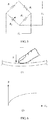
- FIG. 6 a value relationship may be established between the output voltage Uo and the force F, to implement the pressure sensor.
- a finger of a user presses a display. A deformation is caused to the display. The deformation is passed to a resistor. Therefore, a resistance value of the resistor changes, and original bridge balance is broken. The output voltage Uo changes.
- FIG. 6(2) roughly shows the relationship between the output voltage Uo and the force F.
- a larger strain sensitivity coefficient of a material indicates a larger variation of a resistance value. Therefore, if a resistor is made from a material with a larger strain sensitivity coefficient, when an external force is imposed on the screen, a variation of a resistance value of the resistor is larger, and an obtained measurement result of the external force is more accurate.
- the bridge circuit includes a half-bridge circuit (Half Bridge Circuit) and a full bridge circuit (Full Bridge Circuit).
- the circuit shown in FIG. 4 is a full bridge circuit.
- FIG. 5 is a schematic diagram of a half-bridge circuit.
- the half-bridge circuit shown in FIG. 5 is also referred to as a Wheatstone bridge (Wheatstone bridge), a Wheatstone bridge, a Wheatstone bridge, or a one-armed bridge.
- Wheatstone bridge Wheatstone bridge
- U i ⁇ R 4 R 0 + 2 ⁇ R U i
- a relationship between U o and ⁇ R may be calculated by using the formula (5).
- the calculation may be simplified.
- ⁇ R ⁇ R 0 the formula (5) may be simplified to obtain: U o ⁇ ⁇ R 4 R 0 U i
- FIG. 7 is a schematic structural diagram of a display with a pressure sensor.
- the display 104 includes a top surface 1041 and a bottom surface 1042.
- the top surface 1041 and the bottom surface 1042 are two surfaces that are face to face with each other. If the display is an LCD display, the bottom surface 1042 may be a backlight module. If the display is an OLED display, the bottom surface 1042 may be a TFT glass substrate.
- a thin film 202 is disposed on the bottom surface of the display 104.
- the thin film 202 may be a flexible printed circuit (Flexible Printed Circuit, FPC), a polyethylene terephthalate (Polyethylene Terephthalate, PET) material, or the like.
- a bridge array 204 is disposed on the thin film 202. Some areas of the thin film 202 are bonded to the bottom surface 1042, and some areas of the thin film 202 are not bonded to the bottom surface 1042.
- the bridge array 204 is an array including multiple bridge circuits.
- an optical clear adhesive Optically Clear Adhesive, OCA
- the optical clear adhesive is a transparent adhesive.
- FIG. 8 is a locally enlarged schematic diagram of FIG. 7 .
- 2041 is a first bridge circuit
- 2042 is a second bridge circuit
- 2043 is a third bridge circuit.
- 2041, 2042, and 2043 may be the bridge circuits shown in FIG. 4 .
- 2041, 2042, and 2043 may be the bridge circuits shown in FIG. 5 .
- 2041, 2042, and 2043 may be a combination of the bridge circuits shown in FIG. 4 and the bridge circuits shown in FIG. 5 .
- 2041 is the bridge circuit shown in FIG.
- FIG. 4 and 2042 and 2043 are the bridge circuits shown in FIG. 5 .
- a connection manner of resistors R1, R2, R3, and R4 is the same as that of the bridge circuit shown in FIG. 4 .
- Each of the resistors R1, R2, R3, and R4 may be a resistor made from a strain sensitive material. Areas on the thin film 202 in which the resistors R2 and R3 are disposed are bonded to the display 104, and areas on the thin film 202 in which the resistors R1 and R4 are disposed are not bonded to the display 104.
- Some areas near the resistors R1 and R4 are slotted or hollowed out.
- a force is directly or indirectly imposed on the thin film 202, because the areas on the thin film 202 in which the resistors R2 and R3 are disposed are bonded to the display 104, a strain on the thin film 202 is passed to the resistors R2 and R3. Therefore, resistance values of the resistors R2 and R3 change. Because the areas on the thin film 202 in which the resistors R1 and R4 are disposed are not bonded to the display 104, and the areas near the resistors R1 and R4 are slotted or hollowed out, basically, the strain on the thin film 202 is not passed to the resistors R1 and R4.
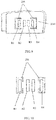
- FIG. 9 is a locally enlarged schematic diagram of FIG. 8 , and 206 indicates slotted or hollowed-out areas. Some areas near the resistor R1 and some areas near the resistor R4 are slotted or hollowed out. An implementation may be further shown in FIG. 10 . Because the resistor is disposed on the thin film, the resistor is bonded to the display. A person skilled in the art may understand that an area on the thin film in which a resistor is disposed is bonded to the display.
- R2 and R3 may be resistors made from materials with a same strain sensitivity coefficient, and R1 and R4 may be fixed-value resistors. Areas on the thin film 202 in which the resistors R2 and R3 are disposed are bonded to the display 104, and areas on the thin film 202 in which the resistors R1 and R4 are disposed are not bonded to the display 104. When a force is directly or indirectly imposed on the thin film 202, a strain on the thin film is passed to the resistors R1, R2, R3, and R4.
- Resistance values of the resistors R2 and R3 change with the strain, and resistance values of the resistors R1 and R4 do not change with the strain because the resistors R1 and R4 are fixed-value resistors. In some other embodiments, further, some areas near the resistors R1 and R4 are slotted or hollowed out.
- an area on the thin film in which a resistor made from a strain sensitive material is disposed is bonded to the bottom surface of the display module, and an area on the thin film in which a fixed-value resistor is disposed is not bonded to the display module. Further, some areas near the fixed-value resistor may be slotted or hollowed out.
- R1, R2, R3, and R4 are made from a same strain sensitive material.
- an external force is imposed on the display 104, for example, a finger of a user presses the display 104, a small deformation is caused to the display 104, and accordingly, a deformation is caused to the thin film 202.
- the resistors R2 and R3 are bonded to the display module, the small deformation may be passed to the resistors R2 and R3.
- the deformation on the thin film 202 is not passed to the resistors R1 and R4 because the resistors R1 and R4 are not bonded to the display module and some areas near the resistors R1 and R4 are hollowed out.
- resistance values of the resistors R2 and R3 change with a strain, and resistance values of the resistors R1 and R4 basically do not change.
- a relationship between an output voltage Uo and a force F may be obtained, so as to determine a user operation according to the force F. For example, if the force imposed by the user is relatively large, an image viewed by the user may be zoomed in; if the force imposed by the user is relatively small, music that is being played by the user may be paused.
- the thin film may be covered by copper, so that the small deformation on the display can be better passed to the bonded resistor.
- a deformation on the resistor bonded to the thin film may be basically the same as the deformation on the display.
- a front surface or a back surface of the thin film may be covered by copper.
- an area on a thin film 402 in which a non-bonded resistor is disposed is not covered by copper.
- copper 404 which is shown in a slashed shadow area and does not include a slotted or hollowed out area 406
- copper removal is performed on the area on the thin film 402 in which the non-bonded resistor is disposed.
- copper in film areas in which resistors R1 and R4 are located is removed in a corroding manner or the like. In this way, the area on the thin film 402 in which the non-bonded resistor is disposed is not covered by copper.
- resistors included in a bridge circuit are resistors included in a bridge circuit. Multiple bridge circuits may be disposed on the thin film 402. The multiple bridge circuits form a bridge array. Setting of another bridge circuit is similar to the setting of the bridge circuit with marks on an upper-left corner of the figure. In this solution, a strain on a resistor bonded to the display can be enhanced, and a possible deformation on a non-bonded resistor may be reduced.
- the thin film may be alternatively covered by a material with a relatively large Young's modulus. Young's modulus is also referred to as Young's modulus (Young's modulus). Covering copper on the thin film is a mature technology and is commonly used, and has a relatively good effect. Table 1 gives Young's moduli of different materials. Generally, a material whose Young's modulus is greater than 30 may be selected. Table 1 Young's moduli of different materials Material Young's modulus (E)/GPa Magnesium 45 Glass 71.7 Aluminum 69 Copper 103-124 Titanium 105-120 Carbon fiber reinforced plastic 150 Alloy and steel 190-210
- copper removal performed on some areas on the thin film in the following solution may also be understood as removal of the material with the relatively large Young's modulus that covers the thin film. It may be understood that removing copper in a corroding manner or the like is a manner for implementing that a film area in which a non-bonded resistor is located is not covered by copper.
- a thin film 502 is covered by copper 504 (which is shown in a slashed shadow area)
- copper removal is performed on areas in which non-bonded resistors R1 and R4 are located and areas near the non-bonded resistors R1 and R4, that is, an area 508 is an area that is not covered by copper, so as to further reduce possible deformations caused to the resistors R1 and R4.
- 506 is a slotted or hollowed out area. A slotting or hollowing out manner may be shown in FIG. 10 .
- resistors in a same bridge circuit may be made from a same strain sensitive material, and may be disposed as close to each other as possible, so that temperatures of the resistors in the same bridge circuit are the same or temperature changes of the resistors in the same bridge circuit are basically the same.
- the resistors R1, R2, R3, and R4 are made from a same strain sensitive material, and are disposed on the thin film as close to each other as possible, so as to reduce a temperature difference between the resistors.
- a manner of processing the resistor R2 in FIG. 5 is similar to a manner of processing the resistors R2 and R3 in FIG. 4
- a manner of processing the resistors R1, R3, and R4 in FIG. 5 is similar to a manner of processing the resistors R1 and R4 in FIG. 4 .
- a bridge circuit on a thin film may be shown in FIG. 4 or FIG. 5 .
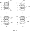
- a slotting manner may be shown in FIG. 14 .
- a slotting manner of the full bridge circuit in FIG. 4 is shown in FIG. 14(3) and FIG. 14(4) .
- 6023 indicates a slotted area, and a resistor in the slotted area, for example, the resistor R3, is not bonded to the display;
- 6043 indicates resistors that are bonded to the display, for example, the resistors R2 and R3.
- FIG. 14(3) 6023 indicates a slotted area, and a resistor in the slotted area, for example, the resistor R3, is not bonded to the display;
- 6043 indicates resistors that are bonded to the display, for example, the resistors R2 and R3.
- 6024 indicates a slotted area, and a resistor in the slotted area, for example, the resistor R2 or R3, is not bonded to the display; 6044 indicates resistors that are bonded to the display, for example, the resistors R1 and R4.
- a slotting manner of the half-bridge circuit shown in FIG. 5 is shown in FIG. 14(2) .
- 6022 indicates a slotted area, and a resistor in the slotted area, for example, the resistor R1, R2, or R4, is not bonded to the display;
- 6042 indicates a resistor that is bonded to the display, for example, the resistor R3.
- FIG. 14(4) 6024 indicates a slotted area, and a resistor in the slotted area, for example, the resistor R2 or R3, is not bonded to the display; 6044 indicates resistors that are bonded to the display, for example, the resistors R1 and R4.
- FIG. 14(2) A slotting manner of the half-bridge circuit shown in FIG. 5 is shown in
- 6021 indicates a slotted area, and a resistor in the slotted area, for example, the resistor R3, is not bonded to the display; 6041 indicates resistors that are bonded to the display, for example, the resistors R1, R2, and R4; this circuit belongs to a full bridge circuit, that is, a circuit with three strain resistors. Resistors that are bonded to the display may be made from materials with basically the same strain sensitive coefficients.
- a thickness of the thin film is approximately 0.1 millimeters.
- an OLED display When an OLED display is disposed in a terminal device, generally, foam is added below the OLED display, to protect an organic light-emitting diode of the OLED display.
- a thin film including a bridge array may be disposed below the foam.
- An embodiment of the present invention provides an electronic device.
- the electronic device is an OLED display with a pressure sensor.
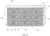
- the OLED display 702 includes a top surface 7201 and a bottom surface 7022.
- the bottom surface of the OLED display 702 may be a TFT glass substrate.
- the top surface 7021 is a surface that is face to face with the bottom surface 7022.
- Foam 704 is disposed on the bottom surface 7022 of the OLED display 702, to protect an organic light-emitting diode of the OLED display.
- a thin film 706 is disposed below the foam 704.
- the thin film may be made from a material such as an FPC or PET.
- a bridge array is disposed on the thin film 706.
- 708 indicates a bridge circuit in the bridge array.
- a connection manner of each bridge circuit may be shown in FIG. 4 or FIG. 5 . Description is given in the following by using an example in which a connection manner of the bridge circuit 708 is the connection manner shown in FIG. 4 .
- Resistors R1, R2, R3, and R4 may be made from a same strain sensitive material, that is, resistance values of the resistors R1, R2, R3, and R4 change with a strain. Some areas of the thin film 706 are bonded to the foam 704, and some areas of the thin film 202 are not bonded to the foam 704. In some embodiments, areas on the thin film in which the resistors R1 and R4 are disposed are not bonded to the foam, and areas on the thin film in which the resistors R2 and R3 are disposed are bonded to the foam.
- areas on the thin film in which the resistors R1 and R4 are disposed are not bonded to the foam, and areas on the thin film in which the resistors R1 and R4 are not disposed are bonded to the foam.
- the areas in which the resistors R1 and R4 are not disposed may include areas in which the resistors R2 and R3 are disposed and an area in which no resistor is disposed.
- the thin-film areas in which the resistors R1 and R4 are located are not bonded to the foam 704; and other areas on the thin film 706 are bonded to the foam 704, including the areas in which the resistors R2 and R3 are located. Because the resistor is disposed on the thin film, the resistor is bonded to the foam. A person skilled in the art may understand that an area on the thin film in which a resistor is disposed is bonded to the foam.
- the resistors R2 and R3 are made from a same strain sensitive material, and the resistors R1 and R4 are fixed-value resistors, that is, resistance values of the resistors R1 and R4 do not change with a strain.
- Some areas of the thin film 706 are bonded to the foam 704, and some areas of the thin film 706 are not bonded to the foam 704.
- an area on the thin film in which a fixed-value resistor is disposed is not bonded to the foam, and an area on the thin film in which a resistor made from a strain sensitive material is disposed is bonded to the foam.
- an area on the thin film in which a fixed-value resistor is disposed is not bonded to the foam, and an area on the thin film in which the fixed-value resistor is not disposed is bonded to the foam.
- the area in which the fixed-value resistor is not disposed may include an area in which a resistor made from a strain sensitive material is disposed and an area in which no resistor is disposed.
- the thin-film areas in which the resistors R1 and R4 are located are not bonded to the foam 704; and other areas on the thin film 706 are bonded to the foam 704, including the areas in which the resistors R2 and R3 are located.
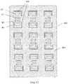
- a front surface or a back surface of the thin film 706 is covered by copper 710 (a shadow area shown in the figure). Copper removal is performed on the areas on the thin film 706 in which the resistors R1 and R4 are disposed.
- a copper removal manner is basically the same as the manner in the embodiment described in FIG. 12 . As shown in FIG. 15 , backgrounds of the resistors R1 and R4 are white, and do not belong to the shadow area indicating the copper 710.
- the thin-film areas in which the resistors R2 and R3 are located are covered by copper and are bonded to the foam, and the thin-film areas in which the resistors R1 and R4 are located are not covered by copper and are not bonded to the foam. Therefore, when a force is imposed on the OLED display, a deformation on the OLED display can be passed to the resistors R2 and R3, and basically cannot be passed to the resistors R1 and R4. In this way, strains in different areas on the film are different.
- resistance values of resistors in different areas on the film change differently.
- the force imposed by a user on the OLED display can be detected according to the difference. For example, whether the force F is greater than a threshold is detected, or whether the force F is less than a threshold is detected.
- the terminal device may perform different operations according to the force.
- a copper-removed area is not completely equal to areas that are occupied by the resistors R1 and R4 on the film.
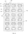
- a thin film 802 is covered by copper 804 (a shadow area shown in the figure), and a copper-removed area includes areas that are occupied by resistors R1 and R4 on the thin film and areas near the resistors R1 and R4.
- An area 806 is an area that is not covered by copper. In this case, the area 806 may indicate an area that is not bonded to foam.
- some areas near the resistors R1 and R4 may be slotted or hollowed out.
- a slotting manner or a hollowing out manner is similar to the solution described in the embodiments of FIG. 7 to FIG. 10 .
- an implementation may be shown in FIG. 12 in which copper removal is performed on areas in which resistors R1 and R4 are located and 406 is a slotted or hollowed out area; or may be shown in FIG. 13 in which 508 is a copper-removed area and 506 is a slotted or hollowed out area.
- the copper-removed areas 508 include areas in which resistors R1 and R4 are located and areas near the resistors R1 and R4.
- resistors in a same bridge circuit may be made from a same strain sensitive material, and may be disposed as close to each other as possible, so that temperatures of the resistors in the same bridge circuit are the same or temperature changes of the resistors in the same bridge circuit are basically the same.
- the resistors R1, R2, R3, and R4 are made from a same strain sensitive material, and are disposed on the thin film as close to each other as possible, so as to reduce a temperature difference between the resistors.
- a connection manner of the bridge circuits 708 is the connection manner shown in FIG. 5
- a manner of processing the resistor R2 in FIG. 5 is similar to a manner of processing the resistors R2 and R3 in FIG. 4
- a manner of processing the resistors R1, R3, and R4 in FIG. 5 is similar to a manner of processing the resistors R1 and R4 in FIG. 4 .
- a thickness of the thin film is approximately 0.1 millimeters.
- an embodiment of the present invention provides a terminal.
- the terminal includes a display described in an embodiment corresponding to FIG. 7 , FIG. 12 , FIG. 13 , FIG. 15 , or FIG. 16 .
- a specific structure of the display is not shown in FIG. 17 .
- description is given by using 912 to indicate a bridge array of the display.
- the bridge array includes multiple bridge circuits. Two bridge circuits are used as an example in the figure.
- a power supply supplies power to the bridge array 912. In an example in which the bridge circuit is connected in the manner in FIG. 4 , before a user presses the display by using a finger or a touch control pen, the bridge is in a balanced state, and an output voltage Uo is 0.
- the bridge balance is broken, and the output voltage Uo changes and is not 0.
- the output voltage Uo of the bridge circuit is relatively small and is hard to obtain by means of direct measurement. Therefore, the output voltage is usually enlarged by using an amplifier; noise is filtered out by using a filter circuit; and then the output voltage is measured.
- the force imposed by the user on the display may be obtained by means of calculation, so as to determine a user operation according to the force F. For example, if the force imposed by the user is relatively large, an image viewed by the user may be zoomed in; if the force imposed by the user is relatively small, music that is being played by the user may be paused.
- an amplifier 904 and an amplifier 908 may be a same amplifier, and a filter circuit 906 and a filter circuit 910 may be a same filter circuit. This is not limited in the present invention.
- the electronic device provided in this embodiment of the present invention may be a display with a pressure sensor.
- the display may further have a touch control function.
- a touch layer is integrated in an LCD display or an OLED display.
- the touch layer may be an indium tin oxide (Indium Tin Oxide, ITO) film.
- ITO Indium Tin Oxide
Landscapes
- Engineering & Computer Science (AREA)
- Theoretical Computer Science (AREA)
- General Engineering & Computer Science (AREA)
- Human Computer Interaction (AREA)
- Physics & Mathematics (AREA)
- General Physics & Mathematics (AREA)
- Computer Hardware Design (AREA)
- Force Measurement Appropriate To Specific Purposes (AREA)
- Electroluminescent Light Sources (AREA)
- Input From Keyboards Or The Like (AREA)
- Devices For Indicating Variable Information By Combining Individual Elements (AREA)
Description
- The present invention relates to the field of display technologies, and in particular, to a display with a pressure sensor, and a terminal.
- Currently, a mainstream display (Display) is also referred to as a display panel. There are two main types of displays: a liquid crystal display (Liquid-Crystal Display, LCD) and an organic light-emitting diode (organic light-emitting diode, OLED) display.
FIG. 1 is a schematic structural diagram of an LCD display and an OLED display. The LCD display includes a backlight unit (Back Light Unit, BLU) 132, abottom polarizer 134, a thin-film transistor (Thin-Film Transistor, TFT)glass layer 136, aliquid crystal layer 138, a color filter (Color Filter, CF) 140, and atop polarizer 142. A structure of the OLED display includes aTFT glass substrate 150, anOLED layer 152, apackage glass 154, and apolarizer 156. - For a detailed description about the OLED display, refer to a webpage of Wikipedia: https://en.wikipedia.org/wiki/OLED (last access time is June 27th, 2016). For a detailed description about the LCD display, refer to a webpage of Wikipedia: https://en.wikipedia.org/wiki/Liquid-crystal display (last access time is June 27th, 2016).
- Currently, many displays further include a touch control layer, and accordingly, this touchable display is referred to as a touchscreen.
- To improve interaction between human and a terminal device such as a mobile phone, a watch, or a wearable device, currently, a pressure sensor is widely applied to parts of the terminal device such as a touchscreen and a housing, so as to identify touch pressure of the user as well as a touch position of the user. Therefore, operation experience with richer content is implemented. A capacitive pressure sensor of Apple company is used as an example. A screen of the mobile phone product iPhone 6s of Apple company is an LCD display.
FIG. 2 is a schematic diagram of an iPhone with a pressure (force) sensing function. Herein, 102 is a cover glass (Cover Glass, CG) of the mobile phone, 104 is a display, and 110 is an iron frame of the mobile phone. There is an extremely thin air gap (air gap) between thedisplay 104 and theiron frame 110. A specific structure of thedisplay 104 may be the LCD display structure shown inFIG. 1 . - A basic principle of the capacitive pressure sensor of Apple company is as follows: A
first electrode 106 is disposed below thedisplay 104, and asecond electrode 108 is disposed above a middle frame (not shown in the figure) or theiron frame 110 of the mobile phone. Thefirst electrode 106, thesecond electrode 108, and the air gap between thefirst electrode 106 and thesecond electrode 108 jointly form a capacitor C. An equivalent circuit of the capacitor C is shown inFIG. 3(1) . The air gap is used as a dielectric of the capacitor C. When the user presses the screen, because there is the air gap between thedisplay 104 and theiron frame 110, a small deformation is caused to the screen in a pressing direction of the user. As shown inFIG. 3(2) , the small deformation causes a change of a capacitance value of the capacitor C, and a variation of the capacitance value is directly proportional to a value of pressure. That is, the variation of the capacitance value may be detected, to detect the value of the pressure. However, the capacitive pressure sensor detects the pressure on the display mainly according to a change of a distance between the dioxides. Therefore, the distance between the dioxides needs to be large enough to ensure accuracy. This increases an overall thickness of the terminal device. - In addition, bottom stacked layers of the OLED display are the TFT and the OLED. The TFT and the OLED are relatively fragile, and have a poor impact resistance capability. Therefore, when the OLED display is applied to the terminal device, a thin foam layer is disposed at the bottom of the OLED display, to mitigate an impact. The foregoing solution of the capacitive pressure sensor is not applicable to the OLED display due to the foam.
-
CN 105 094 49 A describes a pressure sensing input module which includes a first pressure sensing unit and second pressure sensing unit disposed on the upper and lower surfaces of the substrate. - "Application Note 078 Strain Gauge measurements - A tutorial" (Application
- Note 78, National Instruments Corporation) describes the basic principles of measuring strain using a strain gauge, i.e. a device whose electrical resistance varies in proportion to the amount of strain in the device.
- Document
US 2011/0141054 A1 describes a touch pad with force sensors and actuator feedback. The touch pad comprises a capacitive touch sensor having an array of capacitive electrodes. - The document "Residual stress measurement by successive extension of a slot: The crack compliance method" (M.B. Prime et al., Applied Mechanics reviews, Vol.52, No. 2, pages 75-96, 1999) describes the crack compliance method whose goal is to give adequate knowledge of residual stresses.
- A first aspect of the present invention provides an electronic device, where the electronic device is an OLED display with a pressure sensor. In the present invention, a pressure sensor is added on a basis of an existing display. The electronic device includes an OLED display, foam, and a film. The form is located below the OLED display, and the pressure sensor is located below the foam. The pressure sensor includes the film. Multiple bridge circuits are disposed on the film. Each bridge circuit includes a first branch and a second branch. The first branch is connected in parallel to the second branch. The first branch includes a first resistor and a third resistor, and the second branch includes a second resistor and a fourth resistor. A first end of the first resistor is connected to a first end of the second resistor. A second end of the first resistor is connected to a first end of the third resistor. A second end of the second resistor is connected to a first end of the fourth resistor. A second end of the third resistor is connected to a second end of the fourth resistor. The multiple bridge circuits are located on a same side of the film. At least one resistor in the four resistors is bonded to the foam, and at least one resistor is not bonded to the foam. The resistor that is bonded to the foam is made from a first material. A strain sensitivity coefficient of the first material is greater than 100. A film area in which the resistor that is bonded to the foam is located is covered by a second material, and a film area in which the resistor that is not bonded to the foam is located is not covered by the second material. A Young's modulus of the second material is greater than 30. According to this solution, the display with the pressure sensor is implemented, so as to detect a force imposed by a user on the display.
- According to the first aspect, in a first possible implementation of the first aspect, the second resistor and the third resistor are bonded to the foam, and are made from the first material, and the first resistor and the fourth resistor are not bonded to the foam; and film areas in which the second resistor and the third resistor are located are covered by the second material, and film areas in which the first resistor and the fourth resistor are located are not covered by the second material.
- According to the first aspect, in a second possible implementation of the first aspect, the second resistor is bonded to the foam, and is made from the first material, and the first resistor, the third resistor, and the fourth resistor are not bonded to the foam; and a film area in which the second resistor is located is covered by the second material, and film areas in which the first resistor, the third resistor, and the fourth resistor are located are not covered by the second material.
- The first possible implementation of the first aspect and the second possible implementation of the first aspect are two solutions in which pressure detection can be implemented.
- According to any one of the first aspect to the second possible implementation of the first aspect, in a third possible implementation of the first aspect, some film areas near the resistor that is not bonded to the foam are slotted or hollowed out. Because some resistors are not bonded to the foam, and some film areas near the resistors that are not bonded to the foam are slotted or hollowed out, when a force is directly or indirectly imposed on the electronic device, a strain on the resistor that is bonded to the foam is further isolated from a strain on the resistor that is not bonded to the foam.
- According to any one of the first aspect to the third possible implementation of the first aspect, in a fourth possible implementation of the first aspect, the film area in which the resistor that is not bonded to the foam is located and a film area near the resistor that is not bonded to the foam are not covered by the second material. It is easier to implement the manner in which the film area is not covered by the second material. In addition, in this manner, a possible strain on a non-bonded resistor can be further reduced.
- According to any one of the first aspect to the fourth possible implementation of the first aspect, in a fifth possible implementation of the first aspect, the resistor that is not bonded to the foam is made from the first material. That is, the first resistor, the second resistor, the third resistor, and the fourth resistor are made from the same strain sensitive material, so as to simplify a technological process.
- A second aspect of the present invention provides an electronic device, where the electronic device is a display with a pressure sensor. In the present invention, the pressure sensor is added on a basis of an existing display. The display may be an LCE display, or an OLED display. The pressure sensor is located below the display. The pressure sensor includes a film. Multiple bridge circuits are disposed on the film. Each bridge circuit includes a first branch and a second branch. The first branch is connected in parallel to the second branch. The first branch includes a first resistor and a third resistor, and the second branch includes a second resistor and a fourth resistor. A first end of the first resistor is connected to a first end of the second resistor. A second end of the first resistor is connected to a first end of the third resistor. A second end of the second resistor is connected to a first end of the fourth resistor. A second end of the third resistor is connected to a second end of the fourth resistor. The multiple bridge circuits are located on a same side of the film. At least one of the first resistor, the second resistor, the third resistor, or the fourth resistor is bonded to the display, and at least one resistor is not bonded to the display. The resistor that is bonded to the display is made from a first material. A strain sensitivity coefficient of the first material is greater than 100. Some film areas near the resistor that is not bonded to the display are slotted or hollowed out. According to this solution, the display with the pressure sensor is implemented, so as to detect a force imposed by a user on the display.
- According to the second aspect, in a first possible implementation of the second aspect, the second resistor and the third resistor are bonded to the display, and are made from the first material, and the first resistor and the fourth resistor are not bonded to the display; and some film areas near the first resistor and the fourth resistor are slotted or hollowed out.
- According to the second aspect, in a second possible implementation of the second aspect, the second resistor is bonded to the display, and is made from the first material, and the first resistor, the third resistor, and the fourth resistor are not bonded to the display; and some film areas near the first resistor, the third resistor, and the fourth resistor are slotted or hollowed out.
- According to any one of the second aspect to the second possible implementation of the second aspect, in a third possible implementation of the second aspect, a film area in which the resistor that is bonded to the display is located is covered by a second material, and a film area in which the resistor that is not bonded to the display is located is not covered by the second material, where a Young's modulus of the second material is greater than 30. In this solution, a strain on a bonded resistor can be further differentiated from a strain on a non-bonded resistor.
- According to the third possible implementation of the second aspect, in a fourth possible implementation of the second aspect, a film area near the resistor that is not bonded to the foam is not covered by the second material. In this solution, a possible strain on a bonded resistor can be further reduced.
- According to any one of the second aspect to the fourth possible implementation of the second aspect, in a fifth possible implementation of the second aspect, the resistor that is not bonded to the display is made from the first material. The four resistors are made from the same strain sensitive material, so as to simplify a technological process.
- According to any one of the second aspect to the fifth possible implementation of the second aspect, in a sixth possible implementation of the second aspect, the electronic device is a liquid crystal display LCD or an organic light-emitting diode OLED display.
- A third aspect of the present invention provides a terminal. The terminal is a terminal with a pressure sensor display. The terminal includes a power supply and the electronic device provided in the first aspect or the second aspect. The power supply supplies power to each bridge circuit in the electronic device. In each bridge circuit, a first end of the power supply is connected to a first end of a first resistor, and a second end of the power supply is connected to a second end of a third resistor. The bridge circuits are connected in parallel to each other. Each bridge circuit can work independently. The terminal can detect a pressure imposed by a user on the display, to implement a pressure detection operation.
- Optionally, a resistor that is not bonded to foam is a fixed-value resistor. The fixed-value resistor is not bonded to the foam. Therefore, basically, a strain is not passed to the fixed-value resistor. Alternatively, even if a strain is passed to the fixed-value resistor, a resistance value of the fixed-value resistor does not change. The present invention can still be implemented.
- Optionally, the first material is one of the following materials: a carbon-based material, an oxide material, or a semiconductor material. These materials have a relatively large strain sensitivity coefficient each. Therefore, a relatively good effect is achieved by using these materials to make a strain resistor.
- Optionally, the second material is copper. Covering copper on a film is a relatively mature technology by using which the present invention can be simply implemented and a good effect can be achieved.
- Optionally, the film is a flexible printed circuit FPC or a polyethylene terephthalate PET material.
- In this solution, the display with the pressure sensor can be implemented. When the user presses the display, a status of a force imposed by the user on the display can be detected, and a corresponding operation is implemented according to the force status. For example, if it is detected that the force imposed by the user is relatively large, an image displayed on the display may be zoomed in; if it is detected that the force imposed by the user is relatively small, music that is being played may be paused. The electronic device may be a display with a touch function. When detecting a touch operation of the user, the electronic device may further detect a press operation of the user, so as to improve operation experience of the user.
- To describe the technical solutions in the embodiments of the present invention more clearly, the following briefly describes the accompanying drawings required for describing the embodiments. Apparently, the accompanying drawings in the following description show merely some embodiments of the present invention, and a person of ordinary skill in the art may still derive other drawings from these accompanying drawings without creative efforts.
-
FIG. 1 is a schematic structural diagram of an LCD display and an OLED display; -
FIG. 2 is a schematic structural diagram of a screen with a pressure sensor implemented in an iPhone; -
FIG. 3 is a schematic diagram of a principle of a pressure sensor implemented in an iPhone; -
FIG. 4 is a schematic diagram of a full-bridge circuit according to the present invention; -
FIG. 5 is a schematic diagram of a half-bridge circuit according to the present invention; -
FIG. 6 is a schematic diagram of a relationship between an output voltage Uo and a force F according to the present invention; -
FIG. 7 is an electronic device according to the present invention; -
FIG. 8 is a locally enlarged schematic diagram of an electronic device according to the present invention; -
FIG. 9 is another locally enlarged schematic diagram of an electronic device according to the present invention; -
FIG. 10 is a schematic diagram of an implementation for slotting or hollowing out according to the present invention; -
FIG. 11 is a schematic diagram of a pressing principle after hollowing out according to the present invention; -
FIG. 12 is another electronic device according to the present invention; -
FIG. 13 is a schematic diagram of an implementation for copper removal according to the present invention; -
FIG. 14 is a schematic diagram of an implementation for slotting or hollowing out according to the present invention; -
FIG. 15 is another electronic device according to the present invention; -
FIG. 16 is a schematic diagram of another implementation for copper removal according to the present invention; and -
FIG. 17 is a schematic structural diagram of a terminal according to the present invention. - To make the objectives, technical solutions, and advantages of the embodiments of the present invention clearer, the following clearly describes the technical solutions in the embodiments of the present invention with reference to the accompanying drawings in the embodiments of the present invention. Apparently, the described embodiments are a part rather than all of the embodiments of the present invention. All other embodiments obtained by a person of ordinary skill in the art based on the embodiments of the present invention without creative efforts shall fall within the protection scope of the present invention, without departing from the scope of the claims of the present invention.
- A terminal mentioned in the present invention may be, for example, a mobile phone, a tablet computer, a computer display, a computer input device (such as a touch control panel, a keyboard, or a mouse), a wearable device, a health monitor device, or a sports auxiliary device.
- It should be understood that ordinal numbers such as "first" and "second", if mentioned in the embodiments of the present invention, are only used for distinguishing, unless the ordinal numbers definitely represent a sequence according to the context.
- A person skilled in the art easily understands that detailed descriptions about the accompanying drawings provided in this specification are merely for explanation and description and should not be constructed as limitation.
- Generally, a touchscreen of the terminal can detect a touch operation performed by a user on the screen. A touchscreen with a pressure sensor can detect a touch event of the user, and further detect a value of a force imposed by the user on the touchscreen. A touch operation with a pressure may be performed on the touchscreen of the terminal, or another surface related to the terminal. The value of the force detected by the pressure sensor by means of measurement may be used as an input signal, input data, or other input information of the terminal. In an example, an input event generated by a large pressure may be different from an input event generated by a small pressure. For example, when detecting that a pressure exceeds a preset threshold, a smartphone may unlock a display by means of an input event generated by the high force (high force); when detecting that a pressure is less than a preset threshold, a smartphone may pause output of voice by means of an input event generated by the low force (low force). Therefore, even if two pressures are imposed on a same position of a same terminal, responses or outputs of the terminal that are corresponding to the two inputs may be different from each other. Further, in an example, a force change may be explained as an input event of an additional type. For example, the user may keep a wearable device with a force sensor close to an artery, to measure a blood pressure and a heart rate of the user. It can be understood that the force sensor may be configured to collect various types of user inputs.
- In some embodiments, the pressure sensor may be implemented by using a resistor made from a strain sensitive (strain-sensitive) material that is referred to as a strain resistor in the following. (In mechanics, strain is defined as a deformation generated when a stress is imposed on a tiny material element. Strain may be alternatively referred to as a deformation per unit length. Strain is a dimensionless quantity.) This type of resistor is a resistor whose resistance value changes with a strain. For example, when an external force is directly or indirectly imposed on the resistor, a strain of the resistor changes. Therefore, the resistance value of the resistor may change in response to the strain or the external force. A specific variation of the resistance value of the resistor may be measured by using a bridge circuit (Bridge Circuit).
-
FIG. 4 is a schematic diagram of a bridge circuit. The bridge circuit is a full bridge circuit (Full Bridge Circuit). The bridge circuit includes two branches with four bridge arms (Bridge Arm or Bridge Leg), and each of R1, R2, R3, and R4 is located on one bridge arm. A first branch includes the resistors R1 and R3, and a second branch includes the resistors R2 and R4. The first branch is connected in parallel to the second branch. The resistors R1 and R3 are connected in series, and the resistors R2 and R4 are connected in series. Herein, Ui is a constant power supply voltage; the resistors R2 and R3 are strain resistors, and are made from a strain sensitive material; the resistors R1 and R4 are fixed-value resistors, that is, a resistance value of R1 and that of R4 basically do not change with a strain; Uo is an output voltage. The strain sensitive material is generally a material with a relatively large strain sensitivity coefficient. The strain sensitivity coefficient (Gauge Factor) is also referred to as a strain coefficient, a strain sensitive coefficient, a strain sensitivity factor, or a strain gauge sensitivity coefficient. For example, the strain sensitive material may be a carbon-based material, an oxide material, or a semiconductor material. Strain sensitivity coefficients of these materials are mostly greater than 100. When a force is directly or indirectly imposed on a resistor made from a material with a relatively large strain sensitivity coefficient, a resistance value change of the resistor is relatively obvious. - The output voltage Uo may be obtained by means of measurement by using a tool such as a multimeter or an oscillometer. In a circuit of an actual terminal product, the output voltage Uo may be directly obtained by means of reading by using a dedicated circuit and a dedicated component.
- Likewise, the output voltage Uo may be obtained by means of calculation by using the formula:

- It is assumed that a resistance value of R2 and that of R3 both change by ΔR. The formula (1) may change to:

- It is assumed that initial resistance values of the resistors R1, R2, R3, and R4 are all R 0. In this case,

- Therefore, a relationship between U o and ΔR may be obtained:

- Because Ui , U o, and R 0 are known values or can be obtained by means of measurement, ΔR can be obtained, that is, variations of resistance values that are caused due to strains on the resistors R2 and R3.
- Because R2 and R3 are made from the strain sensitive material, the following relationship generally exists:

- Herein, S is a strain sensitivity coefficient (Gauge Factor) that is also referred to as a strain coefficient, a strain sensitive coefficient, a strain sensitivity factor, or a strain gauge sensitivity coefficient, S of a metal material is generally 1.8 to 3.6, and S of a semiconductor material is generally greater than 100. It can be learned that a sensitivity of the semiconductor material is far higher than that of the metal material. ε is a strain. The strain ε is proportional to a force F imposed on the resistor. A larger strain ε indicates a greater force F imposed on the resistor.
- Therefore, as shown in
FIG. 6 , a value relationship may be established between the output voltage Uo and the force F, to implement the pressure sensor. InFIG. 6(1) , a finger of a user presses a display. A deformation is caused to the display. The deformation is passed to a resistor. Therefore, a resistance value of the resistor changes, and original bridge balance is broken. The output voltage Uo changes.FIG. 6(2) roughly shows the relationship between the output voltage Uo and the force F. - In a case of a same strain, a larger strain sensitivity coefficient of a material indicates a larger variation of a resistance value. Therefore, if a resistor is made from a material with a larger strain sensitivity coefficient, when an external force is imposed on the screen, a variation of a resistance value of the resistor is larger, and an obtained measurement result of the external force is more accurate.
- In some embodiments, the bridge circuit includes a half-bridge circuit (Half Bridge Circuit) and a full bridge circuit (Full Bridge Circuit). The circuit shown in
FIG. 4 is a full bridge circuit.FIG. 5 is a schematic diagram of a half-bridge circuit. The half-bridge circuit shown inFIG. 5 is also referred to as a Wheatstone bridge (Wheatstone bridge), a Wheatstone bridge, a Wheatstone bridge, or a one-armed bridge. The following can be obtained by means of calculation:
- A relationship between U o and ΔR may be calculated by using the formula (5).
- In some embodiments, the calculation may be simplified. Generally, ΔR << R 0. Therefore, the formula (5) may be simplified to obtain:

- An embodiment of the present invention provides an electronic device. The electronic device is a display with a pressure sensor.
FIG. 7 is a schematic structural diagram of a display with a pressure sensor. Thedisplay 104 includes atop surface 1041 and abottom surface 1042. Thetop surface 1041 and thebottom surface 1042 are two surfaces that are face to face with each other. If the display is an LCD display, thebottom surface 1042 may be a backlight module. If the display is an OLED display, thebottom surface 1042 may be a TFT glass substrate. Athin film 202 is disposed on the bottom surface of thedisplay 104. Thethin film 202 may be a flexible printed circuit (Flexible Printed Circuit, FPC), a polyethylene terephthalate (Polyethylene Terephthalate, PET) material, or the like. Abridge array 204 is disposed on thethin film 202. Some areas of thethin film 202 are bonded to thebottom surface 1042, and some areas of thethin film 202 are not bonded to thebottom surface 1042. Thebridge array 204 is an array including multiple bridge circuits. Specifically, an optical clear adhesive (Optically Clear Adhesive, OCA) may be used for the bonding. The optical clear adhesive is a transparent adhesive. - To more clearly describe this solution,
FIG. 8 is a locally enlarged schematic diagram ofFIG. 7 . As shown inFIG. 8 , 2041 is a first bridge circuit, 2042 is a second bridge circuit, and 2043 is a third bridge circuit. In some embodiments, 2041, 2042, and 2043 may be the bridge circuits shown inFIG. 4 . In some other embodiments, 2041, 2042, and 2043 may be the bridge circuits shown inFIG. 5 . It may be understood that in some other embodiments, 2041, 2042, and 2043 may be a combination of the bridge circuits shown inFIG. 4 and the bridge circuits shown inFIG. 5 . For example, 2041 is the bridge circuit shown inFIG. 4 , and 2042 and 2043 are the bridge circuits shown inFIG. 5 . Description is given in the following by using an example in which 2041, 2042, and 2043 are the bridge circuits shown inFIG. 4 . In an example of thefirst bridge circuit 2041, a connection manner of resistors R1, R2, R3, and R4 is the same as that of the bridge circuit shown inFIG. 4 . Each of the resistors R1, R2, R3, and R4 may be a resistor made from a strain sensitive material. Areas on thethin film 202 in which the resistors R2 and R3 are disposed are bonded to thedisplay 104, and areas on thethin film 202 in which the resistors R1 and R4 are disposed are not bonded to thedisplay 104. Some areas near the resistors R1 and R4 are slotted or hollowed out. When a force is directly or indirectly imposed on thethin film 202, because the areas on thethin film 202 in which the resistors R2 and R3 are disposed are bonded to thedisplay 104, a strain on thethin film 202 is passed to the resistors R2 and R3. Therefore, resistance values of the resistors R2 and R3 change. Because the areas on thethin film 202 in which the resistors R1 and R4 are disposed are not bonded to thedisplay 104, and the areas near the resistors R1 and R4 are slotted or hollowed out, basically, the strain on thethin film 202 is not passed to the resistors R1 and R4. Therefore, basically, resistance values of the resistors R1 and R4 do not change. Likewise, setting of resistors on another bridge circuit is similar to this solution. To more clearly describe this solution,FIG. 9 is a locally enlarged schematic diagram ofFIG. 8 , and 206 indicates slotted or hollowed-out areas. Some areas near the resistor R1 and some areas near the resistor R4 are slotted or hollowed out. An implementation may be further shown inFIG. 10 . Because the resistor is disposed on the thin film, the resistor is bonded to the display. A person skilled in the art may understand that an area on the thin film in which a resistor is disposed is bonded to the display. - In some embodiments, R2 and R3 may be resistors made from materials with a same strain sensitivity coefficient, and R1 and R4 may be fixed-value resistors. Areas on the
thin film 202 in which the resistors R2 and R3 are disposed are bonded to thedisplay 104, and areas on thethin film 202 in which the resistors R1 and R4 are disposed are not bonded to thedisplay 104. When a force is directly or indirectly imposed on thethin film 202, a strain on the thin film is passed to the resistors R1, R2, R3, and R4. Resistance values of the resistors R2 and R3 change with the strain, and resistance values of the resistors R1 and R4 do not change with the strain because the resistors R1 and R4 are fixed-value resistors. In some other embodiments, further, some areas near the resistors R1 and R4 are slotted or hollowed out. Likewise, in another bridge circuit, an area on the thin film in which a resistor made from a strain sensitive material is disposed is bonded to the bottom surface of the display module, and an area on the thin film in which a fixed-value resistor is disposed is not bonded to the display module. Further, some areas near the fixed-value resistor may be slotted or hollowed out. - As shown in
FIG. 11 , description is given by using an example in which R1, R2, R3, and R4 are made from a same strain sensitive material. When an external force is imposed on thedisplay 104, for example, a finger of a user presses thedisplay 104, a small deformation is caused to thedisplay 104, and accordingly, a deformation is caused to thethin film 202. Because the resistors R2 and R3 are bonded to the display module, the small deformation may be passed to the resistors R2 and R3. The deformation on thethin film 202 is not passed to the resistors R1 and R4 because the resistors R1 and R4 are not bonded to the display module and some areas near the resistors R1 and R4 are hollowed out. Therefore, resistance values of the resistors R2 and R3 change with a strain, and resistance values of the resistors R1 and R4 basically do not change. According to the foregoing described solution, a relationship between an output voltage Uo and a force F may be obtained, so as to determine a user operation according to the force F. For example, if the force imposed by the user is relatively large, an image viewed by the user may be zoomed in; if the force imposed by the user is relatively small, music that is being played by the user may be paused. - In some embodiments, the thin film may be covered by copper, so that the small deformation on the display can be better passed to the bonded resistor. In this way, a deformation on the resistor bonded to the thin film may be basically the same as the deformation on the display. A front surface or a back surface of the thin film may be covered by copper.
- In some embodiments, an area on a
thin film 402 in which a non-bonded resistor is disposed is not covered by copper. As shown inFIG. 12 , after thethin film 402 is evenly covered by copper 404 (which is shown in a slashed shadow area and does not include a slotted or hollowed out area 406), copper removal is performed on the area on thethin film 402 in which the non-bonded resistor is disposed. For example, copper in film areas in which resistors R1 and R4 are located is removed in a corroding manner or the like. In this way, the area on thethin film 402 in which the non-bonded resistor is disposed is not covered by copper. Resistors R1, R2, R3, and R4 shown inFIG. 12 are resistors included in a bridge circuit. Multiple bridge circuits may be disposed on thethin film 402. The multiple bridge circuits form a bridge array. Setting of another bridge circuit is similar to the setting of the bridge circuit with marks on an upper-left corner of the figure. In this solution, a strain on a resistor bonded to the display can be enhanced, and a possible deformation on a non-bonded resistor may be reduced. - In addition to copper, the thin film may be alternatively covered by a material with a relatively large Young's modulus. Young's modulus is also referred to as Young's modulus (Young's modulus). Covering copper on the thin film is a mature technology and is commonly used, and has a relatively good effect. Table 1 gives Young's moduli of different materials. Generally, a material whose Young's modulus is greater than 30 may be selected.
Table 1 Young's moduli of different materials Material Young's modulus (E)/GPa Magnesium 45 Glass 71.7 Aluminum 69 Copper 103-124 Titanium 105-120 Carbon fiber reinforced plastic 150 Alloy and steel 190-210 - If the thin film is covered by another material with a relatively large Young's modulus, copper removal performed on some areas on the thin film in the following solution may also be understood as removal of the material with the relatively large Young's modulus that covers the thin film. It may be understood that removing copper in a corroding manner or the like is a manner for implementing that a film area in which a non-bonded resistor is located is not covered by copper.
- In some other embodiments, as shown in
FIG. 13 , after athin film 502 is covered by copper 504 (which is shown in a slashed shadow area), copper removal is performed on areas in which non-bonded resistors R1 and R4 are located and areas near the non-bonded resistors R1 and R4, that is, anarea 508 is an area that is not covered by copper, so as to further reduce possible deformations caused to the resistors R1 and R4. Herein, 506 is a slotted or hollowed out area. A slotting or hollowing out manner may be shown inFIG. 10 . - In the foregoing embodiment, because of inaccuracy of a manufacturing technology, extremely small deformations may be caused to the non-bonded R1 and R4. In some embodiments, to better isolate strains on R1 and R4 from strains on R2 and R3, an area in which a non-bonded resistor is located and some areas near the non-bonded resistor may be slotted or hollowed out, so that a measurement result of a force is more accurate.
- In some other embodiments, resistors in a same bridge circuit may be made from a same strain sensitive material, and may be disposed as close to each other as possible, so that temperatures of the resistors in the same bridge circuit are the same or temperature changes of the resistors in the same bridge circuit are basically the same. For example, as shown in
FIG. 12 andFIG. 13 , the resistors R1, R2, R3, and R4 are made from a same strain sensitive material, and are disposed on the thin film as close to each other as possible, so as to reduce a temperature difference between the resistors. - If a connection manner of the
bridge circuits FIG. 5 , a manner of processing the resistor R2 inFIG. 5 is similar to a manner of processing the resistors R2 and R3 inFIG. 4 , and a manner of processing the resistors R1, R3, and R4 inFIG. 5 is similar to a manner of processing the resistors R1 and R4 inFIG. 4 . - A bridge circuit on a thin film may be shown in
FIG. 4 orFIG. 5 . Correspondingly, a slotting manner may be shown inFIG. 14 . A slotting manner of the full bridge circuit inFIG. 4 is shown inFIG. 14(3) and FIG. 14(4) . InFIG. 14(3) , 6023 indicates a slotted area, and a resistor in the slotted area, for example, the resistor R3, is not bonded to the display; 6043 indicates resistors that are bonded to the display, for example, the resistors R2 and R3. InFIG. 14(4) , 6024 indicates a slotted area, and a resistor in the slotted area, for example, the resistor R2 or R3, is not bonded to the display; 6044 indicates resistors that are bonded to the display, for example, the resistors R1 and R4. A slotting manner of the half-bridge circuit shown inFIG. 5 is shown inFIG. 14(2) . Herein, 6022 indicates a slotted area, and a resistor in the slotted area, for example, the resistor R1, R2, or R4, is not bonded to the display; 6042 indicates a resistor that is bonded to the display, for example, the resistor R3. InFIG. 14(1) , 6021 indicates a slotted area, and a resistor in the slotted area, for example, the resistor R3, is not bonded to the display; 6041 indicates resistors that are bonded to the display, for example, the resistors R1, R2, and R4; this circuit belongs to a full bridge circuit, that is, a circuit with three strain resistors. Resistors that are bonded to the display may be made from materials with basically the same strain sensitive coefficients. - In the foregoing solution, after the resistors are disposed on the thin film and the thin film is covered by copper, a thickness of the thin film is approximately 0.1 millimeters. In this manner for implementing a pressure sensor, it is unnecessary to add a stress bearing board and use the stress bearing board as an additional stress bearing structure, so as to reduce a thickness of the pressure sensor. Because the stress bearing board does not need to be added, material costs and manufacturing costs can be further reduced in a subsequent assembling phase.
- When an OLED display is disposed in a terminal device, generally, foam is added below the OLED display, to protect an organic light-emitting diode of the OLED display. For the solution in which the foam is disposed below the OLED display, a thin film including a bridge array may be disposed below the foam. An embodiment of the present invention provides an electronic device. The electronic device is an OLED display with a pressure sensor. As shown in
FIG. 15 , theOLED display 702 includes a top surface 7201 and abottom surface 7022. The bottom surface of theOLED display 702 may be a TFT glass substrate. Thetop surface 7021 is a surface that is face to face with thebottom surface 7022.Foam 704 is disposed on thebottom surface 7022 of theOLED display 702, to protect an organic light-emitting diode of the OLED display. Athin film 706 is disposed below thefoam 704. The thin film may be made from a material such as an FPC or PET. A bridge array is disposed on thethin film 706. Herein, 708 indicates a bridge circuit in the bridge array. A connection manner of each bridge circuit may be shown inFIG. 4 orFIG. 5 . Description is given in the following by using an example in which a connection manner of thebridge circuit 708 is the connection manner shown inFIG. 4 . Resistors R1, R2, R3, and R4 may be made from a same strain sensitive material, that is, resistance values of the resistors R1, R2, R3, and R4 change with a strain. Some areas of thethin film 706 are bonded to thefoam 704, and some areas of thethin film 202 are not bonded to thefoam 704. In some embodiments, areas on the thin film in which the resistors R1 and R4 are disposed are not bonded to the foam, and areas on the thin film in which the resistors R2 and R3 are disposed are bonded to the foam. In some other embodiments, areas on the thin film in which the resistors R1 and R4 are disposed are not bonded to the foam, and areas on the thin film in which the resistors R1 and R4 are not disposed are bonded to the foam. The areas in which the resistors R1 and R4 are not disposed may include areas in which the resistors R2 and R3 are disposed and an area in which no resistor is disposed. For example, the thin-film areas in which the resistors R1 and R4 are located are not bonded to thefoam 704; and other areas on thethin film 706 are bonded to thefoam 704, including the areas in which the resistors R2 and R3 are located. Because the resistor is disposed on the thin film, the resistor is bonded to the foam. A person skilled in the art may understand that an area on the thin film in which a resistor is disposed is bonded to the foam. - In some embodiments, the resistors R2 and R3 are made from a same strain sensitive material, and the resistors R1 and R4 are fixed-value resistors, that is, resistance values of the resistors R1 and R4 do not change with a strain. Some areas of the
thin film 706 are bonded to thefoam 704, and some areas of thethin film 706 are not bonded to thefoam 704. In some embodiments, an area on the thin film in which a fixed-value resistor is disposed is not bonded to the foam, and an area on the thin film in which a resistor made from a strain sensitive material is disposed is bonded to the foam. In some other embodiments, an area on the thin film in which a fixed-value resistor is disposed is not bonded to the foam, and an area on the thin film in which the fixed-value resistor is not disposed is bonded to the foam. The area in which the fixed-value resistor is not disposed may include an area in which a resistor made from a strain sensitive material is disposed and an area in which no resistor is disposed. For example, the thin-film areas in which the resistors R1 and R4 are located are not bonded to thefoam 704; and other areas on thethin film 706 are bonded to thefoam 704, including the areas in which the resistors R2 and R3 are located. - A front surface or a back surface of the
thin film 706 is covered by copper 710 (a shadow area shown in the figure). Copper removal is performed on the areas on thethin film 706 in which the resistors R1 and R4 are disposed. A copper removal manner is basically the same as the manner in the embodiment described inFIG. 12 . As shown inFIG. 15 , backgrounds of the resistors R1 and R4 are white, and do not belong to the shadow area indicating thecopper 710. - In the technical solution shown in
FIG. 15 , the thin-film areas in which the resistors R2 and R3 are located are covered by copper and are bonded to the foam, and the thin-film areas in which the resistors R1 and R4 are located are not covered by copper and are not bonded to the foam. Therefore, when a force is imposed on the OLED display, a deformation on the OLED display can be passed to the resistors R2 and R3, and basically cannot be passed to the resistors R1 and R4. In this way, strains in different areas on the film are different. Correspondingly, resistance values of resistors in different areas on the film change differently. The force imposed by a user on the OLED display can be detected according to the difference. For example, whether the force F is greater than a threshold is detected, or whether the force F is less than a threshold is detected. The terminal device may perform different operations according to the force. - In some embodiments, a copper-removed area is not completely equal to areas that are occupied by the resistors R1 and R4 on the film. As shown in
FIG. 16 , athin film 802 is covered by copper 804 (a shadow area shown in the figure), and a copper-removed area includes areas that are occupied by resistors R1 and R4 on the thin film and areas near the resistors R1 and R4. Anarea 806 is an area that is not covered by copper. In this case, thearea 806 may indicate an area that is not bonded to foam. - In some other embodiments, some areas near the resistors R1 and R4 may be slotted or hollowed out. A slotting manner or a hollowing out manner is similar to the solution described in the embodiments of
FIG. 7 to FIG. 10 . In some other embodiments, for a copper-removed area and a slotted area, an implementation may be shown inFIG. 12 in which copper removal is performed on areas in which resistors R1 and R4 are located and 406 is a slotted or hollowed out area; or may be shown inFIG. 13 in which 508 is a copper-removed area and 506 is a slotted or hollowed out area. The copper-removedareas 508 include areas in which resistors R1 and R4 are located and areas near the resistors R1 and R4. - In some other embodiments, resistors in a same bridge circuit may be made from a same strain sensitive material, and may be disposed as close to each other as possible, so that temperatures of the resistors in the same bridge circuit are the same or temperature changes of the resistors in the same bridge circuit are basically the same. For example, as shown in
FIG. 15 andFIG. 16 , the resistors R1, R2, R3, and R4 are made from a same strain sensitive material, and are disposed on the thin film as close to each other as possible, so as to reduce a temperature difference between the resistors. - If a connection manner of the
bridge circuits 708 is the connection manner shown inFIG. 5 , a manner of processing the resistor R2 inFIG. 5 is similar to a manner of processing the resistors R2 and R3 inFIG. 4 , and a manner of processing the resistors R1, R3, and R4 inFIG. 5 is similar to a manner of processing the resistors R1 and R4 inFIG. 4 . - In the foregoing solution, after the resistors are disposed on the thin film and the thin film is covered by copper, a thickness of the thin film is approximately 0.1 millimeters. In this manner for implementing a pressure sensor, it is unnecessary to add a stress bearing board and use the stress bearing board as an additional stress bearing structure, so as to reduce a thickness of the pressure sensor. Because the stress bearing board does not need to be added, material costs and manufacturing costs can be further reduced in a subsequent assembling phase.
- As shown in
FIG. 17 , an embodiment of the present invention provides a terminal. The terminal includes a display described in an embodiment corresponding toFIG. 7 ,FIG. 12 ,FIG. 13 ,FIG. 15 , orFIG. 16 . For ease of description, a specific structure of the display is not shown inFIG. 17 . Instead, description is given by using 912 to indicate a bridge array of the display. The bridge array includes multiple bridge circuits. Two bridge circuits are used as an example in the figure. A power supply supplies power to thebridge array 912. In an example in which the bridge circuit is connected in the manner inFIG. 4 , before a user presses the display by using a finger or a touch control pen, the bridge is in a balanced state, and an output voltage Uo is 0. When the user presses the display by using the finger or the touch control pen, a strain on the display is passed to the resistors R2 and R3. Resistance values of the resistors R2 and R3 change with the strain, and resistance values of the resistors R1 and R4 basically do not change. In this case, the bridge balance is broken, and the output voltage Uo changes and is not 0. Generally, the output voltage Uo of the bridge circuit is relatively small and is hard to obtain by means of direct measurement. Therefore, the output voltage is usually enlarged by using an amplifier; noise is filtered out by using a filter circuit; and then the output voltage is measured. According to the foregoing description in this embodiment, the force imposed by the user on the display may be obtained by means of calculation, so as to determine a user operation according to the force F. For example, if the force imposed by the user is relatively large, an image viewed by the user may be zoomed in; if the force imposed by the user is relatively small, music that is being played by the user may be paused. - In some embodiments, an
amplifier 904 and anamplifier 908 may be a same amplifier, and afilter circuit 906 and afilter circuit 910 may be a same filter circuit. This is not limited in the present invention. - It should be noted that the electronic device provided in this embodiment of the present invention may be a display with a pressure sensor. Certainly, the display may further have a touch control function. For example, a touch layer is integrated in an LCD display or an OLED display. For example, the touch layer may be an indium tin oxide (Indium Tin Oxide, ITO) film. In this way, the display is a display that can detect both a touch operation and a press operation of the user.
- Finally, it should be noted that the foregoing embodiments are merely intended for describing examples of the technical solutions of the present invention other than limiting the present invention. Although the present invention and benefits of the present invention are described in detail with reference to the foregoing embodiments, persons of ordinary skill in the art should understand that they may still make modifications to the technical solutions described in the foregoing embodiments, without departing from the scope of the claims of the present invention.
Claims (13)
- An electronic device, wherein the electronic device comprises an organic light-emitting diode OLED display (702), foam (704), and a film (706), wherein
the foam (704) is located below the OLED display (702), and the film (706) is located below the foam (704);
multiple bridge circuits (708) are disposed on the film (706), each bridge circuit (708) comprises a first branch and a second branch, and the first branch is connected in parallel to the second branch, wherein the first branch comprises a first resistor (R1) and a third resistor (R3), the second branch comprises a second resistor (R2) and a fourth resistor (R4), a first end of the first resistor (R1) is connected to a first end of the second resistor (R2), a second end of the first resistor (R1) is connected to a first end of the third resistor (R3), a second end of the second resistor (R2) is connected to a first end of the fourth resistor (R4), and a second end of the third resistor (R3) is connected to a second end of the fourth resistor (R4), and the multiple bridge circuits (708) are located on a same side of the film (706);
at least one of the first resistor (R1), the second resistor (R2), the third resistor (R3), or the fourth resistor (R4) is bonded to the foam (704), and at least one resistor is not bonded to the foam (704), wherein the resistor that is bonded to the foam (704) is made from a first material, and a strain sensitivity coefficient of the first material is greater than 100; and
a film area in which the resistor that is bonded to the foam (704) is located is covered by a second material, and a film area in which the resistor that is not bonded to the foam (704) is located is not covered by the second material, wherein a Young's modulus of the second material is greater than 30. - The electronic device according to claim 1, wherein
that at least one of the first resistor (R1), the second resistor (R2), the third resistor (R3), or the fourth resistor (R4) is bonded to the foam (704), and at least one resistor is not bonded to the foam (704), wherein the resistor that is bonded to the foam (704) is made from a first material is specifically:the second resistor (R2) and the third resistor (R3) are bonded to the foam (704), and are made from the first material, and the first resistor (R1) and the fourth resistor (R4) are not bonded to the foam (704); andthat a film area in which the resistor that is bonded to the foam (704) is located is covered by a second material, and a film area in which the resistor that is not bonded to the foam (704) is located is not covered by the second material is specifically: film areas in which the second resistor (R2) and the third resistor (R3) are located are covered by the second material, and film areas in which the first resistor (R1) and the fourth resistor (R4) are located are not covered by the second material. - The electronic device according to claim 1, wherein that at least one of the first resistor (R1), the second resistor (R2), the third resistor (R3), or the fourth resistor (R4) is bonded to the foam (704), and at least one resistor is not bonded to the foam (704), wherein the resistor that is bonded to the foam (704) is made from a first material is specifically:the second resistor (R2) is bonded to the foam (704), and is made from the first material, and the first resistor (R1), the third resistor (R3), and the fourth resistor (R4) are not bonded to the foam (704); andthat a film area in which the resistor that is bonded to the foam (704) is located is covered by a second material, and a film area in which the resistor that is not bonded to the foam (704) is located is not covered by the second material is specifically:
a film area in which the second resistor (R2) is located is covered by the second material, and film areas in which the first resistor (R1), the third resistor (R3), and the fourth resistor (R4) are located are not covered by the second material. - The electronic device according to any one of claims 1 to 3, wherein some film areas near the resistor that is not bonded to the foam (704) are slotted or hollowed out.
- The electronic device according to any one of claims 1 to 4, wherein a film area near the resistor that is not bonded to the foam (704) is not covered by the second material.
- The electronic device according to any one of claims 1 to 5, wherein the resistor that is not bonded to the foam (704) is made from the first material.
- An electronic device, wherein the electronic device comprises a display (702) and a film (706), wherein
the film (706) is located below the display (702);
multiple bridge circuits (708) are disposed on the film (706), each bridge circuit (708) comprises a first branch and a second branch, and the first branch is connected in parallel to the second branch, wherein the first branch comprises a first resistor (R1) and a third resistor (R3), the second branch comprises a second resistor (R2) and a fourth resistor (R4), a first end of the first resistor (R1) is connected to a first end of the second resistor, a second end of the first resistor (R1) is connected to a first end of the third resistor (R3), a second end of the second resistor (R2) is connected to a first end of the fourth resistor (R4), and a second end of the third resistor (R3) is connected to a second end of the fourth resistor (R4), and the multiple bridge circuits (708) are located on a same side of the film (706);
at least one of the first resistor (R1), the second resistor (R2), the third resistor (R3), or the fourth resistor (R4) is bonded to the display (702), and at least one resistor (R1) is not bonded to the display (702), wherein the resistor that is bonded to the display (702)is made from a first material, and a strain sensitivity coefficient of the first material is greater than 100; and
some film areas near the resistor that is not bonded to the display (702) are slotted or hollowed out. - The electronic device according to claim 7, wherein
that at least one of the first resistor (R1), the second resistor (R2), the third resistor (R3), or the fourth resistor (R4) is bonded to the display (702), and at least one resistor (R1) is not bonded to the display (702), wherein the resistor that is bonded to the display (702) is made from a first material is specifically:the second resistor (R2) and the third resistor (R3) are bonded to the display (702), and are made from the first material, and the first resistor (R1) and the fourth resistor (R4) are not bonded to the display (702); andthat some film areas near the resistor that is not bonded to the display (702) are slotted or hollowed out is specifically: some film areas near the first resistor (R1) and the fourth resistor (R4) are slotted or hollowed out. - The electronic device according to claim 7, wherein
that at least one of the first resistor (R1), the second resistor (R2), the third resistor (R3), or the fourth resistor (R4) is bonded to the display (702), and at least one resistor (R1) is not bonded to the display (702), wherein the resistor that is bonded to the display (702) is made from a first material is specifically:the second resistor (R2) is bonded to the display (702), and is made from the first material, and the first resistor (R1), the third resistor (R3), and the fourth resistor (R4) are not bonded to the display (702); andthat some film areas near the resistor that is not bonded to the display (702) are slotted or hollowed out is specifically:
some film areas near the first resistor (R1), the third resistor (R3), and the fourth resistor (R4) are slotted or hollowed out. - The electronic device according to any one of claims 7 to 9, wherein a film area in which the resistor that is bonded to the display (702) is located is covered by a second material, and a film area in which the resistor that is not bonded to the display (702) is located is not covered by the second material, wherein a Young's modulus of the second material is greater than 30.
- The electronic device according to claim 10, wherein a film area near the resistor that is not bonded to the display (702) is not covered by the second material.
- The electronic device according to any one of claims 7 to 11, wherein the resistor that is not bonded to the display (702) is made from the first material.
- A terminal, wherein the terminal comprises: a power supply, and the electronic device according to any one of claims 1 to 12, wherein the power supply supplies power to each bridge circuit (708) in the electronic device; and in each bridge circuit (708), a first end of the power supply is connected to a first end of the first resistor (R1), and a second end of the power supply is connected to a second end of a third resistor (R3)
Applications Claiming Priority (1)
| Application Number | Priority Date | Filing Date | Title |
|---|---|---|---|
| PCT/CN2016/087995 WO2018000371A1 (en) | 2016-06-30 | 2016-06-30 | Electronic device and terminal |
Publications (3)
| Publication Number | Publication Date |
|---|---|
| EP3460637A1 EP3460637A1 (en) | 2019-03-27 |
| EP3460637A4 EP3460637A4 (en) | 2019-05-01 |
| EP3460637B1 true EP3460637B1 (en) | 2020-06-03 |
Family
ID=60785039
Family Applications (1)
| Application Number | Title | Priority Date | Filing Date |
|---|---|---|---|
| EP16906771.7A Active EP3460637B1 (en) | 2016-06-30 | 2016-06-30 | Electronic device and terminal |
Country Status (6)
| Country | Link |
|---|---|
| US (1) | US10768743B2 (en) |
| EP (1) | EP3460637B1 (en) |
| JP (1) | JP6764957B2 (en) |
| KR (1) | KR102214010B1 (en) |
| CN (1) | CN108027674B (en) |
| WO (1) | WO2018000371A1 (en) |
Families Citing this family (3)
| Publication number | Priority date | Publication date | Assignee | Title |
|---|---|---|---|---|
| CN107102466B (en) * | 2017-06-30 | 2020-01-21 | 上海天马微电子有限公司 | A display panel and touch display device |
| CN112294279B (en) * | 2020-10-29 | 2024-06-25 | 江西理工大学 | Integrated invasive blood pressure sensor |
| CN112486351A (en) * | 2020-11-27 | 2021-03-12 | 深圳瑞湖科技有限公司 | Pressure sensing device and touch panel |
Citations (1)
| Publication number | Priority date | Publication date | Assignee | Title |
|---|---|---|---|---|
| US20160246420A1 (en) * | 2014-08-14 | 2016-08-25 | Shenzhen New Degree Technology Co.,Ltd. | A preesure sensing structure and a touch-control apparatus |
Family Cites Families (19)
| Publication number | Priority date | Publication date | Assignee | Title |
|---|---|---|---|---|
| JP4617732B2 (en) * | 2004-06-17 | 2011-01-26 | 株式会社日立製作所 | Mechanical quantity measuring device |
| CN1866007B (en) | 2006-05-12 | 2010-06-09 | 中国科学院上海微系统与信息技术研究所 | An integrated piezoresistive silicon dioxide cantilever beam ultra-micro detection sensor, manufacturing method and application |
| JP4958501B2 (en) | 2006-08-30 | 2012-06-20 | 本田技研工業株式会社 | Force sensor chip and external force transmission mechanism |
| US20100123686A1 (en) * | 2008-11-19 | 2010-05-20 | Sony Ericsson Mobile Communications Ab | Piezoresistive force sensor integrated in a display |
| US8633916B2 (en) | 2009-12-10 | 2014-01-21 | Apple, Inc. | Touch pad with force sensors and actuator feedback |
| EP2657812A4 (en) | 2010-12-24 | 2015-06-17 | Graphene Square Inc | Touch sensor using graphin for simultaneously detecting pressure and position |
| EP2788780A1 (en) * | 2011-12-05 | 2014-10-15 | Advanced Microsensors Corporation | Magnetic field sensing apparatus and methods |
| CN102629446B (en) | 2012-03-22 | 2015-08-05 | 京东方科技集团股份有限公司 | Display panel and method of controlling operation thereof thereof and display device |
| EP2693315A1 (en) * | 2012-07-31 | 2014-02-05 | Elo Touch Solutions, Inc. | Touch sensitive display with acoustic isolation |
| AU2015100011B4 (en) | 2014-01-13 | 2015-07-16 | Apple Inc. | Temperature compensating transparent force sensor |
| KR101855027B1 (en) * | 2014-02-12 | 2018-05-04 | 애플 인크. | Force determination employing sheet sensor and capacitive array |
| JP2016092193A (en) * | 2014-11-04 | 2016-05-23 | 日東電工株式会社 | Adhesive conductive cushioning material |
| CN204808289U (en) * | 2015-06-09 | 2015-11-25 | 南昌欧菲光科技有限公司 | Touch -sensitive screen and display device |
| CN204808275U (en) * | 2015-06-10 | 2015-11-25 | 宸鸿科技(厦门)有限公司 | Pressure sensing means |
| CN204740575U (en) | 2015-06-29 | 2015-11-04 | 深圳纽迪瑞科技开发有限公司 | Touch equipment is with pressing recognition device |
| CN105224129B (en) | 2015-09-01 | 2018-06-22 | 宸鸿科技(厦门)有限公司 | A pressure sensing input device |
| CN105094449B (en) | 2015-09-01 | 2018-09-28 | 宸鸿科技(厦门)有限公司 | A kind of pressure-sensing input module |
| CN205334427U (en) * | 2015-12-31 | 2016-06-22 | 华勤通讯技术有限公司 | Mobile terminal and pressure -sensitive device thereof |
| WO2017133016A1 (en) * | 2016-02-06 | 2017-08-10 | 深圳纽迪瑞科技开发有限公司 | Pressure sensor, electronic device, and method for manufacturing pressure sensor |
-
2016
- 2016-06-30 EP EP16906771.7A patent/EP3460637B1/en active Active
- 2016-06-30 CN CN201680026146.0A patent/CN108027674B/en active Active
- 2016-06-30 JP JP2018568763A patent/JP6764957B2/en active Active
- 2016-06-30 US US16/314,418 patent/US10768743B2/en not_active Expired - Fee Related
- 2016-06-30 WO PCT/CN2016/087995 patent/WO2018000371A1/en not_active Ceased
- 2016-06-30 KR KR1020197001642A patent/KR102214010B1/en not_active Expired - Fee Related
Patent Citations (1)
| Publication number | Priority date | Publication date | Assignee | Title |
|---|---|---|---|---|
| US20160246420A1 (en) * | 2014-08-14 | 2016-08-25 | Shenzhen New Degree Technology Co.,Ltd. | A preesure sensing structure and a touch-control apparatus |
Also Published As
| Publication number | Publication date |
|---|---|
| JP6764957B2 (en) | 2020-10-07 |
| CN108027674A (en) | 2018-05-11 |
| EP3460637A4 (en) | 2019-05-01 |
| KR20190018519A (en) | 2019-02-22 |
| JP2019527882A (en) | 2019-10-03 |
| WO2018000371A1 (en) | 2018-01-04 |
| CN108027674B (en) | 2020-11-10 |
| US10768743B2 (en) | 2020-09-08 |
| EP3460637A1 (en) | 2019-03-27 |
| KR102214010B1 (en) | 2021-02-08 |
| US20190171334A1 (en) | 2019-06-06 |
Similar Documents
| Publication | Publication Date | Title |
|---|---|---|
| US11803276B2 (en) | Force sensing architectures | |
| US10928950B2 (en) | Pressure-sensitive touch panel | |
| CN109952553B (en) | Capacitive touch panel with built-in pressure sensor | |
| EP2901255B1 (en) | Pressure sensing display device | |
| KR100997107B1 (en) | Touch input structure for detecting push force and acting position, touch input device and method for detecting push force and acting position using same | |
| EP3293617B1 (en) | Touch sensor, touch detection apparatus and detection method, and touch control device | |
| CN205091721U (en) | Electronic equipment and force transducer who is used for electronic equipment | |
| CN204926052U (en) | Touch display apparatus | |
| JP5042316B2 (en) | Touch panel and display device including the same | |
| CN105739788B (en) | Touch substrate and display device | |
| KR101626299B1 (en) | Adhesion layer-equipped film-shaped pressure-sensitive sensor, and touch pad, protection panel with touch input function, and electronic device which use same | |
| US8711122B2 (en) | Sensor apparatus and information processing apparatus | |
| EP2634553A1 (en) | Temperature sensing device | |
| US20130154998A1 (en) | Electronic Device with Noise-Cancelling Force Sensor | |
| CN104685455A (en) | Input device and control method using input device | |
| JP2005522791A (en) | Touch sensitive display | |
| US10768743B2 (en) | Electronic device and terminal | |
| KR20170074614A (en) | Flexible Display | |
| CN105867682A (en) | Touch control display panel | |
| CN106708300A (en) | Pressure touch unit, manufacture method therefore, and touch display device | |
| Reynolds et al. | 46‐1: Invited Paper: Touch and Display Integration with Force | |
| KR20170040408A (en) | Flexible display device having touch sensor integarted bend sensor | |
| WO2018010292A1 (en) | Force touch structure | |
| WO2017210986A1 (en) | Pressure-sensing touch-control liquid crystal display device, and manufacturing method thereof. | |
| KR100456156B1 (en) | Apparatus And Method For Measuring Linearity Touch Panel |
Legal Events
| Date | Code | Title | Description |
|---|---|---|---|
| STAA | Information on the status of an ep patent application or granted ep patent |
Free format text: STATUS: THE INTERNATIONAL PUBLICATION HAS BEEN MADE |
|
| PUAI | Public reference made under article 153(3) epc to a published international application that has entered the european phase |
Free format text: ORIGINAL CODE: 0009012 |
|
| STAA | Information on the status of an ep patent application or granted ep patent |
Free format text: STATUS: REQUEST FOR EXAMINATION WAS MADE |
|
| 17P | Request for examination filed |
Effective date: 20181219 |
|
| AK | Designated contracting states |
Kind code of ref document: A1 Designated state(s): AL AT BE BG CH CY CZ DE DK EE ES FI FR GB GR HR HU IE IS IT LI LT LU LV MC MK MT NL NO PL PT RO RS SE SI SK SM TR |
|
| AX | Request for extension of the european patent |
Extension state: BA ME |
|
| A4 | Supplementary search report drawn up and despatched |
Effective date: 20190401 |
|
| RIC1 | Information provided on ipc code assigned before grant |
Ipc: G06F 3/041 20060101AFI20190326BHEP |
|
| DAV | Request for validation of the european patent (deleted) | ||
| DAX | Request for extension of the european patent (deleted) | ||
| GRAP | Despatch of communication of intention to grant a patent |
Free format text: ORIGINAL CODE: EPIDOSNIGR1 |
|
| STAA | Information on the status of an ep patent application or granted ep patent |
Free format text: STATUS: GRANT OF PATENT IS INTENDED |
|
| INTG | Intention to grant announced |
Effective date: 20200102 |
|
| GRAS | Grant fee paid |
Free format text: ORIGINAL CODE: EPIDOSNIGR3 |
|
| GRAA | (expected) grant |
Free format text: ORIGINAL CODE: 0009210 |
|
| STAA | Information on the status of an ep patent application or granted ep patent |
Free format text: STATUS: THE PATENT HAS BEEN GRANTED |
|
| AK | Designated contracting states |
Kind code of ref document: B1 Designated state(s): AL AT BE BG CH CY CZ DE DK EE ES FI FR GB GR HR HU IE IS IT LI LT LU LV MC MK MT NL NO PL PT RO RS SE SI SK SM TR |
|
| REG | Reference to a national code |
Ref country code: GB Ref legal event code: FG4D |
|
| REG | Reference to a national code |
Ref country code: CH Ref legal event code: EP Ref country code: AT Ref legal event code: REF Ref document number: 1277688 Country of ref document: AT Kind code of ref document: T Effective date: 20200615 |
|
| REG | Reference to a national code |
Ref country code: DE Ref legal event code: R096 Ref document number: 602016037755 Country of ref document: DE |
|
| REG | Reference to a national code |
Ref country code: LT Ref legal event code: MG4D |
|
| PG25 | Lapsed in a contracting state [announced via postgrant information from national office to epo] |
Ref country code: LT Free format text: LAPSE BECAUSE OF FAILURE TO SUBMIT A TRANSLATION OF THE DESCRIPTION OR TO PAY THE FEE WITHIN THE PRESCRIBED TIME-LIMIT Effective date: 20200603 Ref country code: GR Free format text: LAPSE BECAUSE OF FAILURE TO SUBMIT A TRANSLATION OF THE DESCRIPTION OR TO PAY THE FEE WITHIN THE PRESCRIBED TIME-LIMIT Effective date: 20200904 Ref country code: FI Free format text: LAPSE BECAUSE OF FAILURE TO SUBMIT A TRANSLATION OF THE DESCRIPTION OR TO PAY THE FEE WITHIN THE PRESCRIBED TIME-LIMIT Effective date: 20200603 Ref country code: NO Free format text: LAPSE BECAUSE OF FAILURE TO SUBMIT A TRANSLATION OF THE DESCRIPTION OR TO PAY THE FEE WITHIN THE PRESCRIBED TIME-LIMIT Effective date: 20200903 Ref country code: SE Free format text: LAPSE BECAUSE OF FAILURE TO SUBMIT A TRANSLATION OF THE DESCRIPTION OR TO PAY THE FEE WITHIN THE PRESCRIBED TIME-LIMIT Effective date: 20200603 |
|
| REG | Reference to a national code |
Ref country code: NL Ref legal event code: MP Effective date: 20200603 |
|
| PG25 | Lapsed in a contracting state [announced via postgrant information from national office to epo] |
Ref country code: LV Free format text: LAPSE BECAUSE OF FAILURE TO SUBMIT A TRANSLATION OF THE DESCRIPTION OR TO PAY THE FEE WITHIN THE PRESCRIBED TIME-LIMIT Effective date: 20200603 Ref country code: RS Free format text: LAPSE BECAUSE OF FAILURE TO SUBMIT A TRANSLATION OF THE DESCRIPTION OR TO PAY THE FEE WITHIN THE PRESCRIBED TIME-LIMIT Effective date: 20200603 Ref country code: HR Free format text: LAPSE BECAUSE OF FAILURE TO SUBMIT A TRANSLATION OF THE DESCRIPTION OR TO PAY THE FEE WITHIN THE PRESCRIBED TIME-LIMIT Effective date: 20200603 Ref country code: BG Free format text: LAPSE BECAUSE OF FAILURE TO SUBMIT A TRANSLATION OF THE DESCRIPTION OR TO PAY THE FEE WITHIN THE PRESCRIBED TIME-LIMIT Effective date: 20200903 |
|
| REG | Reference to a national code |
Ref country code: AT Ref legal event code: MK05 Ref document number: 1277688 Country of ref document: AT Kind code of ref document: T Effective date: 20200603 |
|
| PG25 | Lapsed in a contracting state [announced via postgrant information from national office to epo] |
Ref country code: NL Free format text: LAPSE BECAUSE OF FAILURE TO SUBMIT A TRANSLATION OF THE DESCRIPTION OR TO PAY THE FEE WITHIN THE PRESCRIBED TIME-LIMIT Effective date: 20200603 Ref country code: AL Free format text: LAPSE BECAUSE OF FAILURE TO SUBMIT A TRANSLATION OF THE DESCRIPTION OR TO PAY THE FEE WITHIN THE PRESCRIBED TIME-LIMIT Effective date: 20200603 |
|
| PG25 | Lapsed in a contracting state [announced via postgrant information from national office to epo] |
Ref country code: CZ Free format text: LAPSE BECAUSE OF FAILURE TO SUBMIT A TRANSLATION OF THE DESCRIPTION OR TO PAY THE FEE WITHIN THE PRESCRIBED TIME-LIMIT Effective date: 20200603 Ref country code: PT Free format text: LAPSE BECAUSE OF FAILURE TO SUBMIT A TRANSLATION OF THE DESCRIPTION OR TO PAY THE FEE WITHIN THE PRESCRIBED TIME-LIMIT Effective date: 20201006 Ref country code: IT Free format text: LAPSE BECAUSE OF FAILURE TO SUBMIT A TRANSLATION OF THE DESCRIPTION OR TO PAY THE FEE WITHIN THE PRESCRIBED TIME-LIMIT Effective date: 20200603 Ref country code: EE Free format text: LAPSE BECAUSE OF FAILURE TO SUBMIT A TRANSLATION OF THE DESCRIPTION OR TO PAY THE FEE WITHIN THE PRESCRIBED TIME-LIMIT Effective date: 20200603 Ref country code: SM Free format text: LAPSE BECAUSE OF FAILURE TO SUBMIT A TRANSLATION OF THE DESCRIPTION OR TO PAY THE FEE WITHIN THE PRESCRIBED TIME-LIMIT Effective date: 20200603 Ref country code: AT Free format text: LAPSE BECAUSE OF FAILURE TO SUBMIT A TRANSLATION OF THE DESCRIPTION OR TO PAY THE FEE WITHIN THE PRESCRIBED TIME-LIMIT Effective date: 20200603 Ref country code: RO Free format text: LAPSE BECAUSE OF FAILURE TO SUBMIT A TRANSLATION OF THE DESCRIPTION OR TO PAY THE FEE WITHIN THE PRESCRIBED TIME-LIMIT Effective date: 20200603 Ref country code: ES Free format text: LAPSE BECAUSE OF FAILURE TO SUBMIT A TRANSLATION OF THE DESCRIPTION OR TO PAY THE FEE WITHIN THE PRESCRIBED TIME-LIMIT Effective date: 20200603 |
|
| REG | Reference to a national code |
Ref country code: CH Ref legal event code: PL |
|
| PG25 | Lapsed in a contracting state [announced via postgrant information from national office to epo] |
Ref country code: SK Free format text: LAPSE BECAUSE OF FAILURE TO SUBMIT A TRANSLATION OF THE DESCRIPTION OR TO PAY THE FEE WITHIN THE PRESCRIBED TIME-LIMIT Effective date: 20200603 Ref country code: PL Free format text: LAPSE BECAUSE OF FAILURE TO SUBMIT A TRANSLATION OF THE DESCRIPTION OR TO PAY THE FEE WITHIN THE PRESCRIBED TIME-LIMIT Effective date: 20200603 Ref country code: IS Free format text: LAPSE BECAUSE OF FAILURE TO SUBMIT A TRANSLATION OF THE DESCRIPTION OR TO PAY THE FEE WITHIN THE PRESCRIBED TIME-LIMIT Effective date: 20201003 |
|
| REG | Reference to a national code |
Ref country code: DE Ref legal event code: R097 Ref document number: 602016037755 Country of ref document: DE |
|
| PG25 | Lapsed in a contracting state [announced via postgrant information from national office to epo] |
Ref country code: MC Free format text: LAPSE BECAUSE OF FAILURE TO SUBMIT A TRANSLATION OF THE DESCRIPTION OR TO PAY THE FEE WITHIN THE PRESCRIBED TIME-LIMIT Effective date: 20200603 Ref country code: LU Free format text: LAPSE BECAUSE OF NON-PAYMENT OF DUE FEES Effective date: 20200630 |
|
| PLBE | No opposition filed within time limit |
Free format text: ORIGINAL CODE: 0009261 |
|
| STAA | Information on the status of an ep patent application or granted ep patent |
Free format text: STATUS: NO OPPOSITION FILED WITHIN TIME LIMIT |
|
| REG | Reference to a national code |
Ref country code: BE Ref legal event code: MM Effective date: 20200630 |
|
| PG25 | Lapsed in a contracting state [announced via postgrant information from national office to epo] |
Ref country code: IE Free format text: LAPSE BECAUSE OF NON-PAYMENT OF DUE FEES Effective date: 20200630 Ref country code: CH Free format text: LAPSE BECAUSE OF NON-PAYMENT OF DUE FEES Effective date: 20200630 Ref country code: DK Free format text: LAPSE BECAUSE OF FAILURE TO SUBMIT A TRANSLATION OF THE DESCRIPTION OR TO PAY THE FEE WITHIN THE PRESCRIBED TIME-LIMIT Effective date: 20200603 Ref country code: LI Free format text: LAPSE BECAUSE OF NON-PAYMENT OF DUE FEES Effective date: 20200630 |
|
| 26N | No opposition filed |
Effective date: 20210304 |
|
| PG25 | Lapsed in a contracting state [announced via postgrant information from national office to epo] |
Ref country code: BE Free format text: LAPSE BECAUSE OF NON-PAYMENT OF DUE FEES Effective date: 20200630 Ref country code: SI Free format text: LAPSE BECAUSE OF FAILURE TO SUBMIT A TRANSLATION OF THE DESCRIPTION OR TO PAY THE FEE WITHIN THE PRESCRIBED TIME-LIMIT Effective date: 20200603 |
|
| PG25 | Lapsed in a contracting state [announced via postgrant information from national office to epo] |
Ref country code: TR Free format text: LAPSE BECAUSE OF FAILURE TO SUBMIT A TRANSLATION OF THE DESCRIPTION OR TO PAY THE FEE WITHIN THE PRESCRIBED TIME-LIMIT Effective date: 20200603 Ref country code: MT Free format text: LAPSE BECAUSE OF FAILURE TO SUBMIT A TRANSLATION OF THE DESCRIPTION OR TO PAY THE FEE WITHIN THE PRESCRIBED TIME-LIMIT Effective date: 20200603 Ref country code: CY Free format text: LAPSE BECAUSE OF FAILURE TO SUBMIT A TRANSLATION OF THE DESCRIPTION OR TO PAY THE FEE WITHIN THE PRESCRIBED TIME-LIMIT Effective date: 20200603 |
|
| PG25 | Lapsed in a contracting state [announced via postgrant information from national office to epo] |
Ref country code: MK Free format text: LAPSE BECAUSE OF FAILURE TO SUBMIT A TRANSLATION OF THE DESCRIPTION OR TO PAY THE FEE WITHIN THE PRESCRIBED TIME-LIMIT Effective date: 20200603 |
|
| PGFP | Annual fee paid to national office [announced via postgrant information from national office to epo] |
Ref country code: GB Payment date: 20260511 Year of fee payment: 11 |
|
| PGFP | Annual fee paid to national office [announced via postgrant information from national office to epo] |
Ref country code: DE Payment date: 20260506 Year of fee payment: 11 |
|
| PGFP | Annual fee paid to national office [announced via postgrant information from national office to epo] |
Ref country code: FR Payment date: 20260511 Year of fee payment: 11 |