EP3458930B1 - Power supplies with feedback - Google Patents
Power supplies with feedback Download PDFInfo
- Publication number
- EP3458930B1 EP3458930B1 EP17723179.2A EP17723179A EP3458930B1 EP 3458930 B1 EP3458930 B1 EP 3458930B1 EP 17723179 A EP17723179 A EP 17723179A EP 3458930 B1 EP3458930 B1 EP 3458930B1
- Authority
- EP
- European Patent Office
- Prior art keywords
- power supply
- circuit
- current
- voltage
- supply rail
- Prior art date
- Legal status (The legal status is an assumption and is not a legal conclusion. Google has not performed a legal analysis and makes no representation as to the accuracy of the status listed.)
- Active
Links
Images


Classifications
-
- H—ELECTRICITY
- H02—GENERATION; CONVERSION OR DISTRIBUTION OF ELECTRIC POWER
- H02J—ELECTRIC POWER NETWORKS; CIRCUIT ARRANGEMENTS OR SYSTEMS FOR SUPPLYING OR DISTRIBUTING ELECTRIC POWER; SYSTEMS FOR STORING ELECTRIC ENERGY
- H02J4/00—Circuit arrangements for mains or distribution networks not specified as AC or DC; Circuit arrangements for mains or distribution networks combining AC and DC sections or sub-networks
-
- G—PHYSICS
- G06—COMPUTING OR CALCULATING; COUNTING
- G06F—ELECTRIC DIGITAL DATA PROCESSING
- G06F1/00—Details not covered by groups G06F3/00 - G06F13/00 and G06F21/00
- G06F1/26—Power supply means, e.g. regulation thereof
-
- H—ELECTRICITY
- H02—GENERATION; CONVERSION OR DISTRIBUTION OF ELECTRIC POWER
- H02M—APPARATUS FOR CONVERSION BETWEEN AC AND AC, BETWEEN AC AND DC, OR BETWEEN DC AND DC, AND FOR USE WITH MAINS OR SIMILAR POWER SUPPLY SYSTEMS; CONVERSION OF DC OR AC INPUT POWER INTO SURGE OUTPUT POWER; CONTROL OR REGULATION THEREOF
- H02M3/00—Conversion of DC power input into DC power output
- H02M3/02—Conversion of DC power input into DC power output without intermediate conversion into AC
- H02M3/04—Conversion of DC power input into DC power output without intermediate conversion into AC by static converters
- H02M3/10—Conversion of DC power input into DC power output without intermediate conversion into AC by static converters using discharge tubes with control electrode or semiconductor devices with control electrode
- H02M3/145—Conversion of DC power input into DC power output without intermediate conversion into AC by static converters using discharge tubes with control electrode or semiconductor devices with control electrode using devices of a triode or transistor type requiring continuous application of a control signal
- H02M3/155—Conversion of DC power input into DC power output without intermediate conversion into AC by static converters using discharge tubes with control electrode or semiconductor devices with control electrode using devices of a triode or transistor type requiring continuous application of a control signal using semiconductor devices only
- H02M3/156—Conversion of DC power input into DC power output without intermediate conversion into AC by static converters using discharge tubes with control electrode or semiconductor devices with control electrode using devices of a triode or transistor type requiring continuous application of a control signal using semiconductor devices only with automatic control of output voltage or current, e.g. switching regulators
- H02M3/1566—Conversion of DC power input into DC power output without intermediate conversion into AC by static converters using discharge tubes with control electrode or semiconductor devices with control electrode using devices of a triode or transistor type requiring continuous application of a control signal using semiconductor devices only with automatic control of output voltage or current, e.g. switching regulators with means for compensating against rapid load changes, e.g. with auxiliary current source, with dual mode control or with inductance variation
-
- H—ELECTRICITY
- H02—GENERATION; CONVERSION OR DISTRIBUTION OF ELECTRIC POWER
- H02M—APPARATUS FOR CONVERSION BETWEEN AC AND AC, BETWEEN AC AND DC, OR BETWEEN DC AND DC, AND FOR USE WITH MAINS OR SIMILAR POWER SUPPLY SYSTEMS; CONVERSION OF DC OR AC INPUT POWER INTO SURGE OUTPUT POWER; CONTROL OR REGULATION THEREOF
- H02M3/00—Conversion of DC power input into DC power output
- H02M3/02—Conversion of DC power input into DC power output without intermediate conversion into AC
- H02M3/04—Conversion of DC power input into DC power output without intermediate conversion into AC by static converters
- H02M3/10—Conversion of DC power input into DC power output without intermediate conversion into AC by static converters using discharge tubes with control electrode or semiconductor devices with control electrode
- H02M3/145—Conversion of DC power input into DC power output without intermediate conversion into AC by static converters using discharge tubes with control electrode or semiconductor devices with control electrode using devices of a triode or transistor type requiring continuous application of a control signal
- H02M3/155—Conversion of DC power input into DC power output without intermediate conversion into AC by static converters using discharge tubes with control electrode or semiconductor devices with control electrode using devices of a triode or transistor type requiring continuous application of a control signal using semiconductor devices only
- H02M3/156—Conversion of DC power input into DC power output without intermediate conversion into AC by static converters using discharge tubes with control electrode or semiconductor devices with control electrode using devices of a triode or transistor type requiring continuous application of a control signal using semiconductor devices only with automatic control of output voltage or current, e.g. switching regulators
- H02M3/158—Conversion of DC power input into DC power output without intermediate conversion into AC by static converters using discharge tubes with control electrode or semiconductor devices with control electrode using devices of a triode or transistor type requiring continuous application of a control signal using semiconductor devices only with automatic control of output voltage or current, e.g. switching regulators including plural semiconductor devices as final control devices for a single load
- H02M3/1584—Conversion of DC power input into DC power output without intermediate conversion into AC by static converters using discharge tubes with control electrode or semiconductor devices with control electrode using devices of a triode or transistor type requiring continuous application of a control signal using semiconductor devices only with automatic control of output voltage or current, e.g. switching regulators including plural semiconductor devices as final control devices for a single load with a plurality of power processing stages connected in parallel
-
- Y—GENERAL TAGGING OF NEW TECHNOLOGICAL DEVELOPMENTS; GENERAL TAGGING OF CROSS-SECTIONAL TECHNOLOGIES SPANNING OVER SEVERAL SECTIONS OF THE IPC; TECHNICAL SUBJECTS COVERED BY FORMER USPC CROSS-REFERENCE ART COLLECTIONS [XRACs] AND DIGESTS
- Y02—TECHNOLOGIES OR APPLICATIONS FOR MITIGATION OR ADAPTATION AGAINST CLIMATE CHANGE
- Y02P—CLIMATE CHANGE MITIGATION TECHNOLOGIES IN THE PRODUCTION OR PROCESSING OF GOODS
- Y02P80/00—Climate change mitigation technologies for sector-wide applications
- Y02P80/10—Efficient use of energy, e.g. using compressed air or pressurized fluid as energy carrier
- Y02P80/14—District level solutions, i.e. local energy networks
Definitions
- the present disclosure relates to power delivery.
- CMOS complementary metal-oxide-semiconductor
- SoC's systems on a chip
- MCMs multi-chip modules
- Vdd nominal voltage
- the microprocessor When the microprocessor is operating in a low power consumption mode (e.g., drawing only a small or modest current), Vdd should be maintained below some maximum value for Vdd.
- Vdd should be maintained above some minimum value for Vdd.
- External power supply circuits have traditionally been used to supply voltage and current to power supply rails of target circuits, such as microprocessors and the like.
- target circuits such as microprocessors and the like.
- traditional power supply circuit architectures are challenged by the power demands of modern target circuits, where current requirements are increasing, power supply voltages are decreasing, and load current steps are becoming faster and faster.
- US 2015/381026 A1 discloses switching regulator circuits and methods. Cross coupled circuits are provided.
- a first switching regulator stage has an output coupled to a first node, and a second switching regulator stage has an output coupled to a second node.
- the first switching regulator stage includes a feedback input coupled to the second node, and the second switching regulator stage includes a feedback input coupled to the first node.
- the first and second nodes may be coupled together through a capacitor.
- a downstream power supply provides a fast current delivery in response to load current transients and generates a feedback signal to control an upstream power supply so that the upstream and downstream power supplies work together to meet the current and voltage requirements of a target circuit across a wide range of loading conditions.
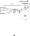
- Fig. 1 illustrates a power supply circuit configuration according to an embodiment.
- Embodiments of the present disclosure include dual power supplies configured to provide power (voltage and current) to a target circuit.
- a (first) local power supply circuit 101 produces a local current I1 and a local voltage VddL to a local power supply rail 111.
- a downstream circuit 104 is configured to receive the local current I1 and the local voltage VddL from the local power supply circuit 101 and produce a remote voltage VddR on a remote power supply rail 110.
- downstream circuits 104 may include parasitic capacitances (e.g., from conductive traces or metals), parasitic inductances (e.g., from package wires or connections), or power distribution fabrics or switches (e.g., from a block head switch (BHS)).
- Remote power supply rail 110 is coupled to a power supply input of a target circuit 103 to provide remove voltage VddR and a load current to the target circuit.
- a second power supply circuit 102 downstream from the local power supply circuit 101 to provide current to the remote power supply rail 110 in response to loading events, such as rapid increases in the current drawn by target circuit 103, for example.
- a second (or remote) power supply circuit 102 has an output coupled to the remote power supply rail 110.
- Downstream circuit 104 may cause a delay in delivering power from the local power supply circuit 101 to the target circuit 103, for example, which may cause VddR on remote power supply rail 110 to droop when a loading event occurs in target circuit 103.
- Remote power supply circuit 102 may be configured near the target circuit 103, for example.
- remote power supply circuit 102 may be physically smaller in size than local power supply circuit 101 and may have a different topology. Accordingly, remote power supply circuit 102 may be configured to respond to a loading event on the remote power supply rail 110 faster than the local power supply circuit 101, for example. In some embodiments, the remote power supply circuit 102 may provide a current within a first time period in response to the loading event, while the local power supply circuit 101 may provide a current and/or a voltage within a second period that is longer than the first time period in response to the loading event.
- remote power supply circuit 102 may be coupled to a second remote power supply rail 150, which may have a higher voltage value Vdd2 than VddR on rail 110 (Vdd2 > VddR), for example, to couple energy into remote power supply rail 110 quickly in response to loading events.
- remote power supply circuit 102 may be configured to sense a loading event on remote power supply rail 110, which due to the proximity of the remote power supply circuit to the target circuit may provide for much faster response times.
- remote power supply circuit 102 provides a remote current 12 to the remote power supply rail 110 for target circuit 103 in response to a loading event, e.g., from the circuit 103 and/or on the rail 110.
- Remote power supply circuit 102 may include a sense circuit 107 to sense a loading event.
- remote power supply circuit configurations may include voltage sensors, current sensors, or clock sensors, for example, to sense a loading event. Accordingly, sense circuits in remote power supply circuit 102 may sense current or receive voltage VddR or a clock signal at 108 from target circuit 103.
- Embodiments of the present disclosure may advantageously include a remote power supply circuit 102 that generates a remote feedback signal produced in response to a loading event and coupled to local power supply circuit 101, for example.
- local power supply circuit 101 is configured to receive the remote feedback signal and produce a local current I1 and a local voltage VddL to a local power supply rail 111 in response to the remote feedback signal.
- local power supply circuit 101 may also receive a local feedback signal based on local voltage VddL on rail 111, for example.
- one power supply circuit may provide fast transient power to a target circuit in response to loading events, and another power supply circuit may receive a feedback signal indicating that the loading event has occurred so the voltage and current can be modified to meet the changing downstream loading requirements of the target circuit.
- local power supply circuit 101 may be the primary source of power for the target circuit 103 and the second power supply circuit 102 may primarily provide transient power to target circuit 103, for example. Because power supply circuit 102 provides a remote feedback signal to power supply circuit 101, power supply circuit 102 is referred to herein as the "remote" power supply and power supply circuit 101 is referred to herein as the "local" power supply. Those skilled in the art will recognize that this is merely a naming convention and that the names could be reversed or other names could be utilized.
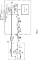
- Fig. 2 illustrates an example power supply circuit configuration according to another embodiment.
- local power supply circuit 201 is a switching regulator comprising a high side switch 210, a low side switch 211, an inductor 212, and an output capacitor 213.
- Switches 210 and 211 may be MOS transistors, for example.
- the switching regulator receives a power supply input voltage, Vddin, and produces a local power supply rail voltage VddL, which is regulated by local and remote feedback signals ("FB L " and "FB R ") at the input of control circuit 214.
- Vddin is greater than VddL
- the switching regulator is a Buck switching regulator, for example.
- local feedback 250 may be provided from capacitor 213 or a point farther downstream such as capacitance 233, for example.
- VddL is coupled through a downstream circuit 203 comprising parasitic capacitance 231, 233, and 236, parasitic inductance 232 and 234, and a block head switch (BHS) 235 to produce a remote power supply rail voltage VddR.
- the BHS provides a way to disconnect the target circuit 103 in Fig. 1 , or Processor 204, from the remote supply rail 110 in Fig 1 , or VddR, in order to reduce the power consumption during times of Target Circuit 103, or Processor 204, inactivity.
- the downsteam circuit in this example may include parasitics L and C associated with the boundary 205 of an integrated circuit (IC) or multi-chip module (MSM) package.
- BHS 235 may distribute VddL to target circuits on the IC such as processor 204 and/or one or more other processors 290, for example, each of which may also include a remote power supply circuit as described herein.
- the remote voltage VddR on the remote power supply voltage rail 216 at parasitic capacitors 236 is coupled to processor 204.
- the supply 201 may in some embodiments be implemented in a power management integrated circuit (PMIC), which may be separate from and/or external to the package defined by the boundary 205.
- PMIC power management integrated circuit
- remote power supply circuit 202 comprises a circuit for delivering packets of charge to rail 216.
- circuit 202 includes a PMOS transistor 222 having a first terminal coupled to the remote power supply rail 216, a second terminal coupled to a second remote power supply rail 227 having a voltage Vdd2 greater than VddR.
- Power supply rail 227 may be driven by another off package power supply 226, for example, which may provide a second on-package rail voltage greater than VddR.
- a control terminal of transistor 222 is driven by a one shot circuit 221.
- Circuit 221 turns ON transistor 222 for a predetermined time period in response to receiving a load event signal to deliver a packet of charge from Vdd2 to VddR to maintain VddR from drooping in response to an increase in load current.
- One-shot circuit 221 has an input coupled to receive the load event signal generated by a sense circuit 220(described below) and an output coupled to the control terminal of transistor 222.
- the sense circuit 220 is a clock sense circuit to sense a loading event and generate a load event signal.
- the loading event in this case may be when a particular processor clock turns ON, for example, which may indicate that the processor load current is going to increase. Because one-shot 221 and transistor 222 deliver packets of charge (or coulombs), these components together are sometimes referred to as a "coulomb cannon.”
- the load event signal is also the remote feedback signal.
- the load event signal is generated to trigger the one-shot 221 to turn the PMOS 222 ON for a predetermined time period (i.e., fire the coulomb cannon).
- the load event signal is also transmitted to a remote feedback input, FB R , of control circuit 214 to adjust the operation of local power supply 201.
- local feedback may implement a voltage control loop and/or a current control loop, and the remote feedback may cause the high side transistor to turn ON.
- the high side transistor may be triggered to turn ON and OFF during a typical switching regulator cycle by a latch in the control circuit 214.
- Receiving the remote feedback signal at the remote feedback input may trigger a latch to turn the high side switching transistor ON (e.g., immediately) to couple Vddin to the local power supply rail 215 for a predetermined time period, which may be greater than the typical time period the high side transistor is typically ON during a cycle.
- the high side switch may be turned ON early during a pulse width modulation switching cycle and remain ON for the remainder of the cycle and possibly one or more subsequent cycles, for example.
- the ON time of the high side switching transistor is increased during or more duty cycles of the switching regulator.
- the remote feedback signal may be introduced into the voltage control loop or the current control loop, for example. The result is to increase the switching regulator output current or output voltage or both to quickly provide more power downstream to compensate for a loading event.
- a package may include many target circuits, such as one or more processors on a signal IC or module. Each such processor may have a similar remote power supply circuit 202. Accordingly, each of the processors may generate load event signals, which may be combined in an OR gate (shown in dashed lines in Fig. 2 ) and used as the remote feedback signals to cause local power supply circuit 201 to respond to loading events from multiple different processors.
- Fig. 2 also illustrates a low side coulomb cannon 229 and low side transistor 228 for sensing increases in the rail voltage VddR and discharging packets of charge to maintain VddR below some maximum nominal value.
- Fig. 3 illustrates another example power supply circuit configuration according to an embodiment.
- the remote feedback signal may modify the local feedback signal to increase the local current from the local power supply when a remote voltage on the remote power supply rail drops below a nominal value.
- the remote feedback signal and the local feedback signal are combined using capacitor 351 and resistor 350 to produce a modified feedback signal to control circuit 300.
- a load event signal is a positive pulse which is inverted by pulldown 352 and AC coupled through capacitor 351 into the feedback path of the local power supply circuit.
- Capacitor 351 has a first terminal configured to receive the remote feedback signal and a second terminal coupled to a feedback input (FB) of the local power supply and to the power supply rail 315 (e.g., through resistor 350).
- FB feedback input
- the negative pulse of the remote feedback signal results in the feedback input being reduced (the local power supply output appears lower than it actually is for the period of the pulse), which causes the local power supply to increase the local voltage VddL (and current) for a predetermined time period, for example.
- a load event signal is generated, which causes the coulomb cannon to fire charge into the remote power supply rail 310 and also reduce the feedback FB (e.g., a voltage) to the local power supply.
- the time period for closing transistor 222 e.g., the size of the charge packets
- a remote power supply circuit 400 includes an amplifier 401 and a current sensor (e.g., resistor 402 and amplifier 403).
- Amplifier 401 has an input coupled to a reference voltage, Vset, and an output coupled to the remote power supply rail 410.
- Vset a reference voltage
- VddR is compared to Vset.
- Vset e.g., in response to a loading event
- amplifier 401 may produce an output current Io into rail 410.
- the output current is sensed by resistor 402 to produce a voltage, which is sensed by amplifier 403.
- Amplifier 403 in turn, produces a remote feedback signal, which in this case is a signal that corresponds to the current into the rail 410 from remote power supply 400.
- the feedback signal may be incorporated into the feedback loop of control circuit 451 to cause local power supply 201 to produce more voltage or current as needed to meet the current demands of the target circuit (here, a processor 204).
- the mechanism for sensing current from the remote power supply to the remote power supply rail to generate the remote feedback signal is implemented using a resistor and amplifier.
- other current sensor circuits and configurations could also be used such as parallel sense transistor circuits, for example.
- an averaging circuit 450 is configured to receive the feedback signal and produce an average, for example.
- the averaging circuit 450 may have an input coupled to a current sensor in remote power supply circuit 400 to receive the remote feedback signal and an output coupled to a feedback input (FB) of the local power supply 201.
- FB feedback input
- local power supply may respond to an average current from remote power supply 400 to produce average current to the target circuit, for example.
- Example averaging circuits may include a filter (e.g., a low pass filter (LPF)), integrator, or proportional-integral-differential (PID) control circuit, for example.
- LPF low pass filter
- PID proportional-integral-differential
- Fig. 5 illustrates another example power supply circuit configuration according to an embodiment.
- remote power supply circuit 500 includes a switching regulator 501 having an input coupled to a second remote power supply rail 227 having a voltage Vdd2 greater than a voltage VddR on remote power supply rail 510.
- Switching regulator 501 further includes a control input coupled to a reference voltage, Vset, for setting the output voltage of the regulator, for example.
- Switching regulator 501 has an output coupled to the remote power supply rail 510 to produce an output current Io.
- the switching regulator further includes a feedback input coupled to the remote power supply rail 510 to sense voltage VddR.
- VddR is compared to Vset, and when VddR starts to deviate from a nominal value of Vset (e.g., due to a loading event), switching regulator 501 responds by driving current Io into or out of remote power supply rail 510 to drive VddR back to Vset, for example.
- the switching regulator input Vdd2 is greater than the output VddR, the switching regulator is a Buck switching regulator (i.e., Vin > Vout).
- Remote power supply circuit 500 further includes a current sensor 503 configured to sense current from the output of the switching regulator 501 to the remote power supply rail 510, and in accordance therewith, generate a remote feedback signal.
- the remote feedback signal is coupled to a feedback input (FB) of a control circuit 551 of an upstream local power supply circuit 201.
- FB feedback input
- the feedback signal may be received by an averaging circuit 450 so that local power supply circuit 201 produces an average of the current being produced by remote power supply circuit 500.
- remote power supply circuit 500 may be a smaller, faster switching regulator configured to respond to load transients and produce transient currents, and local power supply circuit 500 may be a larger, slower switching regulator configured to drive slower average currents.
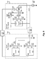
- Fig. 6 illustrates another example power supply circuit configuration according to an embodiment.
- local power supply circuit 690 includes a multiphase switching regulator comprising multiple inductors 612 and 617 driven by two switching stages including switches 610/611 and 615/616 to produce voltage VddL on capacitor 618 (voltage and current control loops not shown).
- VddL is coupled through a delay circuit 650, such as parasitic inductances and capacitances, for example, to produce a downstream remote power supply rail voltage VddR on load 695.
- remote power supply circuit 691 includes both a high speed linear amplifier and a high efficiency switching regulator configured to maintain VddR at a predetermined value, such as Vset, for example.
- the switching regulator comprises switches 630/631 coupled between a second remote power supply rail voltage Vdd2 and ground, where Vdd2 > VddR and the switching regulator is a Buck switching regulator (i.e., Vin > Vout).
- An intermediate switching node between the switches is coupled though an inductor 632 to VddR.
- VddR Voltage on the output of the switching regulator is VddR, which is regulated by control circuit 634 having a control input coupled to a reference voltage, Vset, a feedback input coupled to VddR, and driver outputs to turn switches 630/631 ON and OFF.
- a linear amplifier 637 is powered between Vdd2 and ground, and may have one input coupled to Vset and a second input coupled to the output of the linear amplifier in a unity gain configuration, where the output of the linear amplifier is coupled to VddR. Accordingly, when VddR deviates from a nominal value set by Vset, the linear amplifier responds fastest with an output current Io1 and the switching regulator responds with a more efficient Io2 to maintain VddR at a nominal value.
- a current sense circuit includes a series resistor 635 coupled between the load 695 and the outputs of the switching regulator and linear amplifier.
- a differential sense amplifier 636 translates a differential voltage across resistor 635 into a feedback signal corresponding to the current being driven into the load to maintain the load at a nominal value.
- the feedback signal which also corresponds to a loading event, may be averaged by circuit 651 and provided to feedback inputs of the switching regulator in the upstream local power supply circuit 690.
- Fig. 7 illustrates a method of supplying power according to an embodiment.
- a downstream power supply e.g., a coulomb cannon or Buck converter
- an upstream power supply e.g., a larger Buck or Buck with greater power, current, and/or voltage output
- a voltage and a current may be produced by a first power supply (e.g., the power supply 101, 201, and/or 690).
- the voltage and current from the first power supply may be produced in response to a downstream feedback signal, and may further be produced in response to local feedback, for example.
- the first power supply configured to produce current and voltage in response to a loading event on a downstream power supply rail within a first time period.
- the voltage and current are coupled to the downstream power supply rail for a target circuit.
- the voltage and current from the first power supply may be coupled through various downstream circuits (e.g., circuits 104, 203, 650, and/or one or more elements illustrated in Figs.
- 3-5 between the supply 201 and the processor 204 such as parasitic capacitance and parasitic inductance, which may cause delays between a time of the loading event on the downstream power supply rail and the time the first power supply can respond with increased current, for example.
- current is produced from a second power supply (e.g., the power supply 102, 202, 400, 500, and/or 691).
- the second power supply may be arranged near the load to respond faster to loading events, for example.
- the current is produced from the second power supply to the downstream power supply rail in response to loading events.
- the second power supply may be configured to be smaller and faster than the first power supply to provide smaller transient currents quickly in response to rapidly changing current demands of a target circuit, for example.
- the current may be produced within a second time period that is shorter than the first time period.
- the downstream feedback signal is generated in response to the loading event and provided to the first power supply.
- the first power supply may receive the feedback signal and increase an output current to meet the current demands of the load.
Landscapes
- Engineering & Computer Science (AREA)
- Power Engineering (AREA)
- Theoretical Computer Science (AREA)
- Physics & Mathematics (AREA)
- General Engineering & Computer Science (AREA)
- General Physics & Mathematics (AREA)
- Dc-Dc Converters (AREA)
- Power Sources (AREA)
Applications Claiming Priority (3)
| Application Number | Priority Date | Filing Date | Title |
|---|---|---|---|
| US201662338614P | 2016-05-19 | 2016-05-19 | |
| US15/192,840 US10122179B2 (en) | 2016-05-19 | 2016-06-24 | Power supplies with feedback |
| PCT/US2017/028308 WO2017200689A1 (en) | 2016-05-19 | 2017-04-19 | Power supplies with feedback |
Publications (2)
| Publication Number | Publication Date |
|---|---|
| EP3458930A1 EP3458930A1 (en) | 2019-03-27 |
| EP3458930B1 true EP3458930B1 (en) | 2020-07-08 |
Family
ID=58701847
Family Applications (1)
| Application Number | Title | Priority Date | Filing Date |
|---|---|---|---|
| EP17723179.2A Active EP3458930B1 (en) | 2016-05-19 | 2017-04-19 | Power supplies with feedback |
Country Status (8)
| Country | Link |
|---|---|
| US (1) | US10122179B2 (cg-RX-API-DMAC7.html) |
| EP (1) | EP3458930B1 (cg-RX-API-DMAC7.html) |
| JP (1) | JP6870004B2 (cg-RX-API-DMAC7.html) |
| KR (1) | KR102488507B1 (cg-RX-API-DMAC7.html) |
| CN (1) | CN109154851B (cg-RX-API-DMAC7.html) |
| BR (1) | BR112018073456A2 (cg-RX-API-DMAC7.html) |
| TW (1) | TW201813269A (cg-RX-API-DMAC7.html) |
| WO (1) | WO2017200689A1 (cg-RX-API-DMAC7.html) |
Families Citing this family (4)
| Publication number | Priority date | Publication date | Assignee | Title |
|---|---|---|---|---|
| US10461643B1 (en) * | 2018-04-04 | 2019-10-29 | Nanohenry, Inc. | Composite embedded voltage regulator (CEVR) |
| US20190377405A1 (en) * | 2019-03-29 | 2019-12-12 | Intel Corporation | Input Voltage Protection |
| US11228244B2 (en) | 2019-09-25 | 2022-01-18 | Dialog Semiconductor (Uk) Limited | Power converter supporting multiple high dl/dt loads |
| US12438460B1 (en) | 2024-08-07 | 2025-10-07 | Novatek Microelectronics Corp. | Power management circuit capable of reducing power consumption of electronic devices |
Family Cites Families (23)
| Publication number | Priority date | Publication date | Assignee | Title |
|---|---|---|---|---|
| US6130526A (en) * | 1999-04-02 | 2000-10-10 | Semtech Corporation | Voltage regulator with wide control bandwidth |
| US6181120B1 (en) * | 1999-09-01 | 2001-01-30 | Intersil Corporation | Current mode dc/dc converter with controlled output impedance |
| CN1398031A (zh) * | 2001-07-16 | 2003-02-19 | 松下电器产业株式会社 | 电源装置 |
| US6643158B2 (en) * | 2001-10-31 | 2003-11-04 | Mobility Electronics, Inc. | Dual input AC/DC to programmable DC output converter |
| US6900697B1 (en) * | 2002-05-31 | 2005-05-31 | National Semiconductor Corporation | Method and system for providing power management in a radio frequency power amplifier by dynamically adjusting supply and bias conditions |
| CN100419614C (zh) * | 2002-11-28 | 2008-09-17 | 华邦电子股份有限公司 | 具有平衡电流的多通道脉波宽度调变转换器 |
| US20060022653A1 (en) | 2004-07-29 | 2006-02-02 | Reed Byron M | System and method to mitigate transient energy |
| US7202646B2 (en) | 2004-08-02 | 2007-04-10 | Vlt, Inc. | Control interface with droop compensation |
| US7421593B2 (en) * | 2004-11-19 | 2008-09-02 | Intel Corporation | Parallel-connected voltage regulators for supplying power to integrated circuit so that second regulator minimizes current output from first regulator |
| US7592789B2 (en) | 2005-10-31 | 2009-09-22 | Chil Semiconductor Corporation | Power supply and related circuits |
| US20080191667A1 (en) * | 2007-02-12 | 2008-08-14 | Fyrestorm, Inc. | Method for charging a battery using a constant current adapted to provide a constant rate of change of open circuit battery voltage |
| CN101567627B (zh) * | 2008-04-21 | 2011-07-06 | 英业达股份有限公司 | 电源模块 |
| US8243410B2 (en) | 2008-05-07 | 2012-08-14 | Intel Corporation | Transient voltage compensation system and method |
| US9300202B2 (en) | 2012-05-10 | 2016-03-29 | Intersil Americas LLC | System and method of dynamic droop for switched mode regulators |
| JP6315834B2 (ja) * | 2012-08-10 | 2018-04-25 | 日本テキサス・インスツルメンツ株式会社 | スイッチトモードアシストリニアレギュレータ |
| US20140181546A1 (en) * | 2012-12-24 | 2014-06-26 | Alan D. Hallberg | Method and apparatus for power resource protection |
| US9735574B2 (en) * | 2012-12-31 | 2017-08-15 | Gazelle Semiconductor, Inc. | Switching regulator circuits and methods |
| US9086708B2 (en) * | 2012-12-31 | 2015-07-21 | Gazelle Semiconductor Inc. | High slew rate switching regulator circuits and methods |
| US8981829B1 (en) | 2013-08-29 | 2015-03-17 | International Business Machines Corporation | Passgate strength calibration techniques for voltage regulators |
| US9191013B1 (en) | 2013-10-24 | 2015-11-17 | Seagate Technology Llc | Voltage compensation |
| US9459689B2 (en) | 2013-12-23 | 2016-10-04 | Intel Corporation | Dyanamically adapting a voltage of a clock generation circuit |
| US9397567B2 (en) | 2014-02-05 | 2016-07-19 | Apple Inc. | Shunt integrated voltage regulator |
| US9444340B2 (en) * | 2014-06-26 | 2016-09-13 | Gazelle Semiconductor, Inc. | Circuits and methods for providing current to a load |
-
2016
- 2016-06-24 US US15/192,840 patent/US10122179B2/en active Active
-
2017
- 2017-04-19 CN CN201780030750.5A patent/CN109154851B/zh active Active
- 2017-04-19 BR BR112018073456-0A patent/BR112018073456A2/pt active Search and Examination
- 2017-04-19 WO PCT/US2017/028308 patent/WO2017200689A1/en not_active Ceased
- 2017-04-19 EP EP17723179.2A patent/EP3458930B1/en active Active
- 2017-04-19 JP JP2018560647A patent/JP6870004B2/ja not_active Expired - Fee Related
- 2017-04-19 KR KR1020187033330A patent/KR102488507B1/ko active Active
- 2017-05-09 TW TW106115221A patent/TW201813269A/zh unknown
Non-Patent Citations (1)
| Title |
|---|
| None * |
Also Published As
| Publication number | Publication date |
|---|---|
| US10122179B2 (en) | 2018-11-06 |
| CN109154851A (zh) | 2019-01-04 |
| CN109154851B (zh) | 2022-05-31 |
| KR102488507B1 (ko) | 2023-01-12 |
| KR20190009751A (ko) | 2019-01-29 |
| BR112018073456A2 (pt) | 2019-03-26 |
| TW201813269A (zh) | 2018-04-01 |
| JP6870004B2 (ja) | 2021-05-12 |
| EP3458930A1 (en) | 2019-03-27 |
| US20170338662A1 (en) | 2017-11-23 |
| WO2017200689A1 (en) | 2017-11-23 |
| JP2019517237A (ja) | 2019-06-20 |
Similar Documents
| Publication | Publication Date | Title |
|---|---|---|
| US11552564B1 (en) | Power conversion circuit with solid-state switches | |
| US7777462B2 (en) | Power supply unit | |
| US9548654B2 (en) | DC-DC converter with temperature, process and voltage compensated dead time delay | |
| CN100474750C (zh) | 能够快速响应输入及输出电压变化的供电方法和电源设备 | |
| JP3614156B2 (ja) | 電源回路 | |
| CN106575127B (zh) | 具有电容管理的功率供给拓扑 | |
| CN101071984B (zh) | 直流-直流变换器和用于直流-直流变换器的控制器 | |
| US8975776B2 (en) | Fast start-up voltage regulator | |
| EP3458930B1 (en) | Power supplies with feedback | |
| CN109964396B (zh) | 瞬态事件检测器电路及方法 | |
| CN101218735A (zh) | 降压型开关调节器及其控制电路、使用了它的电子设备 | |
| CN101789682B (zh) | 一种多路输出电源时序控制装置及方法 | |
| KR20130066266A (ko) | 부하변동 특성 향상을 위한 전압공급 회로 및 출력전압 공급 방법 | |
| KR20130108202A (ko) | 타이밍 제어형 인덕터 바이패스를 이용하는 부스트 조절기 | |
| CN103259409A (zh) | 电压转换电路 | |
| US20130099846A1 (en) | Driving circuit, semiconductor device having driving circuit, and switching regulator and electronic equipment using driving circuit and semiconductor device | |
| CN104253531A (zh) | 电路 | |
| US20230261624A1 (en) | Comparator, Oscillator, and Power Converter | |
| CN104410300B (zh) | 同步整流驱动电路及电视机 | |
| US9397571B2 (en) | Controlled delivery of a charging current to a boost capacitor of a voltage regulator | |
| US9236798B2 (en) | DC-DC converter control circuit and DC-DC converter | |
| JP2009207256A (ja) | 降圧型スイッチングレギュレータ | |
| US20230318442A1 (en) | Battery surge reduction based on early warning signal | |
| TWI425755B (zh) | 可減緩電源突波的脈波寬度調變降壓轉化器及其相關方法 | |
| Lin et al. | A low-power regulator for display driver IC requiring a moderate current drivability |
Legal Events
| Date | Code | Title | Description |
|---|---|---|---|
| STAA | Information on the status of an ep patent application or granted ep patent |
Free format text: STATUS: UNKNOWN |
|
| STAA | Information on the status of an ep patent application or granted ep patent |
Free format text: STATUS: THE INTERNATIONAL PUBLICATION HAS BEEN MADE |
|
| PUAI | Public reference made under article 153(3) epc to a published international application that has entered the european phase |
Free format text: ORIGINAL CODE: 0009012 |
|
| STAA | Information on the status of an ep patent application or granted ep patent |
Free format text: STATUS: REQUEST FOR EXAMINATION WAS MADE |
|
| 17P | Request for examination filed |
Effective date: 20181011 |
|
| AK | Designated contracting states |
Kind code of ref document: A1 Designated state(s): AL AT BE BG CH CY CZ DE DK EE ES FI FR GB GR HR HU IE IS IT LI LT LU LV MC MK MT NL NO PL PT RO RS SE SI SK SM TR |
|
| AX | Request for extension of the european patent |
Extension state: BA ME |
|
| DAV | Request for validation of the european patent (deleted) | ||
| DAX | Request for extension of the european patent (deleted) | ||
| GRAP | Despatch of communication of intention to grant a patent |
Free format text: ORIGINAL CODE: EPIDOSNIGR1 |
|
| STAA | Information on the status of an ep patent application or granted ep patent |
Free format text: STATUS: GRANT OF PATENT IS INTENDED |
|
| INTG | Intention to grant announced |
Effective date: 20200206 |
|
| GRAS | Grant fee paid |
Free format text: ORIGINAL CODE: EPIDOSNIGR3 |
|
| GRAA | (expected) grant |
Free format text: ORIGINAL CODE: 0009210 |
|
| STAA | Information on the status of an ep patent application or granted ep patent |
Free format text: STATUS: THE PATENT HAS BEEN GRANTED |
|
| AK | Designated contracting states |
Kind code of ref document: B1 Designated state(s): AL AT BE BG CH CY CZ DE DK EE ES FI FR GB GR HR HU IE IS IT LI LT LU LV MC MK MT NL NO PL PT RO RS SE SI SK SM TR |
|
| REG | Reference to a national code |
Ref country code: CH Ref legal event code: EP Ref country code: AT Ref legal event code: REF Ref document number: 1289143 Country of ref document: AT Kind code of ref document: T Effective date: 20200715 |
|
| REG | Reference to a national code |
Ref country code: DE Ref legal event code: R096 Ref document number: 602017019383 Country of ref document: DE |
|
| REG | Reference to a national code |
Ref country code: IE Ref legal event code: FG4D |
|
| REG | Reference to a national code |
Ref country code: LT Ref legal event code: MG4D |
|
| REG | Reference to a national code |
Ref country code: AT Ref legal event code: MK05 Ref document number: 1289143 Country of ref document: AT Kind code of ref document: T Effective date: 20200708 |
|
| REG | Reference to a national code |
Ref country code: NL Ref legal event code: MP Effective date: 20200708 |
|
| PG25 | Lapsed in a contracting state [announced via postgrant information from national office to epo] |
Ref country code: FI Free format text: LAPSE BECAUSE OF FAILURE TO SUBMIT A TRANSLATION OF THE DESCRIPTION OR TO PAY THE FEE WITHIN THE PRESCRIBED TIME-LIMIT Effective date: 20200708 Ref country code: PT Free format text: LAPSE BECAUSE OF FAILURE TO SUBMIT A TRANSLATION OF THE DESCRIPTION OR TO PAY THE FEE WITHIN THE PRESCRIBED TIME-LIMIT Effective date: 20201109 Ref country code: NO Free format text: LAPSE BECAUSE OF FAILURE TO SUBMIT A TRANSLATION OF THE DESCRIPTION OR TO PAY THE FEE WITHIN THE PRESCRIBED TIME-LIMIT Effective date: 20201008 Ref country code: AT Free format text: LAPSE BECAUSE OF FAILURE TO SUBMIT A TRANSLATION OF THE DESCRIPTION OR TO PAY THE FEE WITHIN THE PRESCRIBED TIME-LIMIT Effective date: 20200708 Ref country code: ES Free format text: LAPSE BECAUSE OF FAILURE TO SUBMIT A TRANSLATION OF THE DESCRIPTION OR TO PAY THE FEE WITHIN THE PRESCRIBED TIME-LIMIT Effective date: 20200708 Ref country code: GR Free format text: LAPSE BECAUSE OF FAILURE TO SUBMIT A TRANSLATION OF THE DESCRIPTION OR TO PAY THE FEE WITHIN THE PRESCRIBED TIME-LIMIT Effective date: 20201009 Ref country code: BG Free format text: LAPSE BECAUSE OF FAILURE TO SUBMIT A TRANSLATION OF THE DESCRIPTION OR TO PAY THE FEE WITHIN THE PRESCRIBED TIME-LIMIT Effective date: 20201008 Ref country code: SE Free format text: LAPSE BECAUSE OF FAILURE TO SUBMIT A TRANSLATION OF THE DESCRIPTION OR TO PAY THE FEE WITHIN THE PRESCRIBED TIME-LIMIT Effective date: 20200708 Ref country code: LT Free format text: LAPSE BECAUSE OF FAILURE TO SUBMIT A TRANSLATION OF THE DESCRIPTION OR TO PAY THE FEE WITHIN THE PRESCRIBED TIME-LIMIT Effective date: 20200708 Ref country code: HR Free format text: LAPSE BECAUSE OF FAILURE TO SUBMIT A TRANSLATION OF THE DESCRIPTION OR TO PAY THE FEE WITHIN THE PRESCRIBED TIME-LIMIT Effective date: 20200708 |
|
| PG25 | Lapsed in a contracting state [announced via postgrant information from national office to epo] |
Ref country code: PL Free format text: LAPSE BECAUSE OF FAILURE TO SUBMIT A TRANSLATION OF THE DESCRIPTION OR TO PAY THE FEE WITHIN THE PRESCRIBED TIME-LIMIT Effective date: 20200708 Ref country code: RS Free format text: LAPSE BECAUSE OF FAILURE TO SUBMIT A TRANSLATION OF THE DESCRIPTION OR TO PAY THE FEE WITHIN THE PRESCRIBED TIME-LIMIT Effective date: 20200708 Ref country code: LV Free format text: LAPSE BECAUSE OF FAILURE TO SUBMIT A TRANSLATION OF THE DESCRIPTION OR TO PAY THE FEE WITHIN THE PRESCRIBED TIME-LIMIT Effective date: 20200708 Ref country code: IS Free format text: LAPSE BECAUSE OF FAILURE TO SUBMIT A TRANSLATION OF THE DESCRIPTION OR TO PAY THE FEE WITHIN THE PRESCRIBED TIME-LIMIT Effective date: 20201108 |
|
| PG25 | Lapsed in a contracting state [announced via postgrant information from national office to epo] |
Ref country code: NL Free format text: LAPSE BECAUSE OF FAILURE TO SUBMIT A TRANSLATION OF THE DESCRIPTION OR TO PAY THE FEE WITHIN THE PRESCRIBED TIME-LIMIT Effective date: 20200708 |
|
| REG | Reference to a national code |
Ref country code: DE Ref legal event code: R097 Ref document number: 602017019383 Country of ref document: DE |
|
| PG25 | Lapsed in a contracting state [announced via postgrant information from national office to epo] |
Ref country code: IT Free format text: LAPSE BECAUSE OF FAILURE TO SUBMIT A TRANSLATION OF THE DESCRIPTION OR TO PAY THE FEE WITHIN THE PRESCRIBED TIME-LIMIT Effective date: 20200708 Ref country code: EE Free format text: LAPSE BECAUSE OF FAILURE TO SUBMIT A TRANSLATION OF THE DESCRIPTION OR TO PAY THE FEE WITHIN THE PRESCRIBED TIME-LIMIT Effective date: 20200708 Ref country code: SM Free format text: LAPSE BECAUSE OF FAILURE TO SUBMIT A TRANSLATION OF THE DESCRIPTION OR TO PAY THE FEE WITHIN THE PRESCRIBED TIME-LIMIT Effective date: 20200708 Ref country code: RO Free format text: LAPSE BECAUSE OF FAILURE TO SUBMIT A TRANSLATION OF THE DESCRIPTION OR TO PAY THE FEE WITHIN THE PRESCRIBED TIME-LIMIT Effective date: 20200708 Ref country code: DK Free format text: LAPSE BECAUSE OF FAILURE TO SUBMIT A TRANSLATION OF THE DESCRIPTION OR TO PAY THE FEE WITHIN THE PRESCRIBED TIME-LIMIT Effective date: 20200708 Ref country code: CZ Free format text: LAPSE BECAUSE OF FAILURE TO SUBMIT A TRANSLATION OF THE DESCRIPTION OR TO PAY THE FEE WITHIN THE PRESCRIBED TIME-LIMIT Effective date: 20200708 |
|
| PLBE | No opposition filed within time limit |
Free format text: ORIGINAL CODE: 0009261 |
|
| STAA | Information on the status of an ep patent application or granted ep patent |
Free format text: STATUS: NO OPPOSITION FILED WITHIN TIME LIMIT |
|
| PG25 | Lapsed in a contracting state [announced via postgrant information from national office to epo] |
Ref country code: AL Free format text: LAPSE BECAUSE OF FAILURE TO SUBMIT A TRANSLATION OF THE DESCRIPTION OR TO PAY THE FEE WITHIN THE PRESCRIBED TIME-LIMIT Effective date: 20200708 |
|
| 26N | No opposition filed |
Effective date: 20210409 |
|
| PG25 | Lapsed in a contracting state [announced via postgrant information from national office to epo] |
Ref country code: SK Free format text: LAPSE BECAUSE OF FAILURE TO SUBMIT A TRANSLATION OF THE DESCRIPTION OR TO PAY THE FEE WITHIN THE PRESCRIBED TIME-LIMIT Effective date: 20200708 |
|
| PG25 | Lapsed in a contracting state [announced via postgrant information from national office to epo] |
Ref country code: SI Free format text: LAPSE BECAUSE OF FAILURE TO SUBMIT A TRANSLATION OF THE DESCRIPTION OR TO PAY THE FEE WITHIN THE PRESCRIBED TIME-LIMIT Effective date: 20200708 |
|
| PG25 | Lapsed in a contracting state [announced via postgrant information from national office to epo] |
Ref country code: MC Free format text: LAPSE BECAUSE OF FAILURE TO SUBMIT A TRANSLATION OF THE DESCRIPTION OR TO PAY THE FEE WITHIN THE PRESCRIBED TIME-LIMIT Effective date: 20200708 |
|
| PG25 | Lapsed in a contracting state [announced via postgrant information from national office to epo] |
Ref country code: LU Free format text: LAPSE BECAUSE OF NON-PAYMENT OF DUE FEES Effective date: 20210419 |
|
| REG | Reference to a national code |
Ref country code: BE Ref legal event code: MM Effective date: 20210430 |
|
| PG25 | Lapsed in a contracting state [announced via postgrant information from national office to epo] |
Ref country code: FR Free format text: LAPSE BECAUSE OF NON-PAYMENT OF DUE FEES Effective date: 20210430 Ref country code: CH Free format text: LAPSE BECAUSE OF NON-PAYMENT OF DUE FEES Effective date: 20210430 Ref country code: LI Free format text: LAPSE BECAUSE OF NON-PAYMENT OF DUE FEES Effective date: 20210430 |
|
| PG25 | Lapsed in a contracting state [announced via postgrant information from national office to epo] |
Ref country code: IE Free format text: LAPSE BECAUSE OF NON-PAYMENT OF DUE FEES Effective date: 20210419 |
|
| PG25 | Lapsed in a contracting state [announced via postgrant information from national office to epo] |
Ref country code: IS Free format text: LAPSE BECAUSE OF FAILURE TO SUBMIT A TRANSLATION OF THE DESCRIPTION OR TO PAY THE FEE WITHIN THE PRESCRIBED TIME-LIMIT Effective date: 20201108 |
|
| PG25 | Lapsed in a contracting state [announced via postgrant information from national office to epo] |
Ref country code: BE Free format text: LAPSE BECAUSE OF NON-PAYMENT OF DUE FEES Effective date: 20210430 |
|
| PG25 | Lapsed in a contracting state [announced via postgrant information from national office to epo] |
Ref country code: CY Free format text: LAPSE BECAUSE OF FAILURE TO SUBMIT A TRANSLATION OF THE DESCRIPTION OR TO PAY THE FEE WITHIN THE PRESCRIBED TIME-LIMIT Effective date: 20200708 |
|
| PG25 | Lapsed in a contracting state [announced via postgrant information from national office to epo] |
Ref country code: HU Free format text: LAPSE BECAUSE OF FAILURE TO SUBMIT A TRANSLATION OF THE DESCRIPTION OR TO PAY THE FEE WITHIN THE PRESCRIBED TIME-LIMIT; INVALID AB INITIO Effective date: 20170419 |
|
| PG25 | Lapsed in a contracting state [announced via postgrant information from national office to epo] |
Ref country code: MK Free format text: LAPSE BECAUSE OF FAILURE TO SUBMIT A TRANSLATION OF THE DESCRIPTION OR TO PAY THE FEE WITHIN THE PRESCRIBED TIME-LIMIT Effective date: 20200708 |
|
| PGFP | Annual fee paid to national office [announced via postgrant information from national office to epo] |
Ref country code: GB Payment date: 20240314 Year of fee payment: 8 |
|
| PG25 | Lapsed in a contracting state [announced via postgrant information from national office to epo] |
Ref country code: TR Free format text: LAPSE BECAUSE OF FAILURE TO SUBMIT A TRANSLATION OF THE DESCRIPTION OR TO PAY THE FEE WITHIN THE PRESCRIBED TIME-LIMIT Effective date: 20200708 |
|
| PG25 | Lapsed in a contracting state [announced via postgrant information from national office to epo] |
Ref country code: MT Free format text: LAPSE BECAUSE OF FAILURE TO SUBMIT A TRANSLATION OF THE DESCRIPTION OR TO PAY THE FEE WITHIN THE PRESCRIBED TIME-LIMIT Effective date: 20200708 |
|
| PGFP | Annual fee paid to national office [announced via postgrant information from national office to epo] |
Ref country code: DE Payment date: 20250317 Year of fee payment: 9 |
|
| GBPC | Gb: european patent ceased through non-payment of renewal fee |
Effective date: 20250419 |
|
| PG25 | Lapsed in a contracting state [announced via postgrant information from national office to epo] |
Ref country code: GB Free format text: LAPSE BECAUSE OF NON-PAYMENT OF DUE FEES Effective date: 20250419 |