EP3456698A1 - Method for manufacturing metal-ceramic substrate with trimmed resistors and metal-ceramic substrate with trimmed resistors - Google Patents
Method for manufacturing metal-ceramic substrate with trimmed resistors and metal-ceramic substrate with trimmed resistors Download PDFInfo
- Publication number
- EP3456698A1 EP3456698A1 EP17190803.1A EP17190803A EP3456698A1 EP 3456698 A1 EP3456698 A1 EP 3456698A1 EP 17190803 A EP17190803 A EP 17190803A EP 3456698 A1 EP3456698 A1 EP 3456698A1
- Authority
- EP
- European Patent Office
- Prior art keywords
- metal layer
- conductive metal
- ablation
- thickness
- layer
- Prior art date
- Legal status (The legal status is an assumption and is not a legal conclusion. Google has not performed a legal analysis and makes no representation as to the accuracy of the status listed.)
- Granted
Links
Images

Classifications
-
- C—CHEMISTRY; METALLURGY
- C04—CEMENTS; CONCRETE; ARTIFICIAL STONE; CERAMICS; REFRACTORIES
- C04B—LIME, MAGNESIA; SLAG; CEMENTS; COMPOSITIONS THEREOF, e.g. MORTARS, CONCRETE OR LIKE BUILDING MATERIALS; ARTIFICIAL STONE; CERAMICS; REFRACTORIES; TREATMENT OF NATURAL STONE
- C04B37/00—Joining burned ceramic articles with other burned ceramic articles or other articles by heating
- C04B37/02—Joining burned ceramic articles with other burned ceramic articles or other articles by heating with metallic articles
- C04B37/021—Joining burned ceramic articles with other burned ceramic articles or other articles by heating with metallic articles in a direct manner, e.g. direct copper bonding [DCB]
-
- B—PERFORMING OPERATIONS; TRANSPORTING
- B23—MACHINE TOOLS; METAL-WORKING NOT OTHERWISE PROVIDED FOR
- B23K—SOLDERING OR UNSOLDERING; WELDING; CLADDING OR PLATING BY SOLDERING OR WELDING; CUTTING BY APPLYING HEAT LOCALLY, e.g. FLAME CUTTING; WORKING BY LASER BEAM
- B23K26/00—Working by laser beam, e.g. welding, cutting or boring
- B23K26/0006—Working by laser beam, e.g. welding, cutting or boring taking account of the properties of the material involved
-
- B—PERFORMING OPERATIONS; TRANSPORTING
- B23—MACHINE TOOLS; METAL-WORKING NOT OTHERWISE PROVIDED FOR
- B23K—SOLDERING OR UNSOLDERING; WELDING; CLADDING OR PLATING BY SOLDERING OR WELDING; CUTTING BY APPLYING HEAT LOCALLY, e.g. FLAME CUTTING; WORKING BY LASER BEAM
- B23K26/00—Working by laser beam, e.g. welding, cutting or boring
- B23K26/02—Positioning or observing the workpiece, e.g. with respect to the point of impact; Aligning, aiming or focusing the laser beam
- B23K26/03—Observing, e.g. monitoring, the workpiece
-
- B—PERFORMING OPERATIONS; TRANSPORTING
- B23—MACHINE TOOLS; METAL-WORKING NOT OTHERWISE PROVIDED FOR
- B23K—SOLDERING OR UNSOLDERING; WELDING; CLADDING OR PLATING BY SOLDERING OR WELDING; CUTTING BY APPLYING HEAT LOCALLY, e.g. FLAME CUTTING; WORKING BY LASER BEAM
- B23K26/00—Working by laser beam, e.g. welding, cutting or boring
- B23K26/02—Positioning or observing the workpiece, e.g. with respect to the point of impact; Aligning, aiming or focusing the laser beam
- B23K26/06—Shaping the laser beam, e.g. by masks or multi-focusing
- B23K26/062—Shaping the laser beam, e.g. by masks or multi-focusing by direct control of the laser beam
- B23K26/0622—Shaping the laser beam, e.g. by masks or multi-focusing by direct control of the laser beam by shaping pulses
- B23K26/0624—Shaping the laser beam, e.g. by masks or multi-focusing by direct control of the laser beam by shaping pulses using ultrashort pulses, i.e. pulses of 1 ns or less
-
- B—PERFORMING OPERATIONS; TRANSPORTING
- B23—MACHINE TOOLS; METAL-WORKING NOT OTHERWISE PROVIDED FOR
- B23K—SOLDERING OR UNSOLDERING; WELDING; CLADDING OR PLATING BY SOLDERING OR WELDING; CUTTING BY APPLYING HEAT LOCALLY, e.g. FLAME CUTTING; WORKING BY LASER BEAM
- B23K26/00—Working by laser beam, e.g. welding, cutting or boring
- B23K26/08—Devices involving relative movement between laser beam and workpiece
- B23K26/082—Scanning systems, i.e. devices involving movement of the laser beam relative to the laser head
-
- B—PERFORMING OPERATIONS; TRANSPORTING
- B23—MACHINE TOOLS; METAL-WORKING NOT OTHERWISE PROVIDED FOR
- B23K—SOLDERING OR UNSOLDERING; WELDING; CLADDING OR PLATING BY SOLDERING OR WELDING; CUTTING BY APPLYING HEAT LOCALLY, e.g. FLAME CUTTING; WORKING BY LASER BEAM
- B23K26/00—Working by laser beam, e.g. welding, cutting or boring
- B23K26/351—Working by laser beam, e.g. welding, cutting or boring for trimming or tuning of electrical components
-
- B—PERFORMING OPERATIONS; TRANSPORTING
- B23—MACHINE TOOLS; METAL-WORKING NOT OTHERWISE PROVIDED FOR
- B23K—SOLDERING OR UNSOLDERING; WELDING; CLADDING OR PLATING BY SOLDERING OR WELDING; CUTTING BY APPLYING HEAT LOCALLY, e.g. FLAME CUTTING; WORKING BY LASER BEAM
- B23K26/00—Working by laser beam, e.g. welding, cutting or boring
- B23K26/36—Removing material
- B23K26/361—Removing material for deburring or mechanical trimming
-
- B—PERFORMING OPERATIONS; TRANSPORTING
- B23—MACHINE TOOLS; METAL-WORKING NOT OTHERWISE PROVIDED FOR
- B23K—SOLDERING OR UNSOLDERING; WELDING; CLADDING OR PLATING BY SOLDERING OR WELDING; CUTTING BY APPLYING HEAT LOCALLY, e.g. FLAME CUTTING; WORKING BY LASER BEAM
- B23K26/00—Working by laser beam, e.g. welding, cutting or boring
- B23K26/36—Removing material
- B23K26/40—Removing material taking account of the properties of the material involved
-
- H—ELECTRICITY
- H01—ELECTRIC ELEMENTS
- H01C—RESISTORS
- H01C17/00—Apparatus or processes specially adapted for manufacturing resistors
- H01C17/22—Apparatus or processes specially adapted for manufacturing resistors adapted for trimming
- H01C17/24—Apparatus or processes specially adapted for manufacturing resistors adapted for trimming by removing or adding resistive material
- H01C17/242—Apparatus or processes specially adapted for manufacturing resistors adapted for trimming by removing or adding resistive material by laser
-
- H—ELECTRICITY
- H05—ELECTRIC TECHNIQUES NOT OTHERWISE PROVIDED FOR
- H05K—PRINTED CIRCUITS; CASINGS OR CONSTRUCTIONAL DETAILS OF ELECTRIC APPARATUS; MANUFACTURE OF ASSEMBLAGES OF ELECTRICAL COMPONENTS
- H05K1/00—Printed circuits
- H05K1/02—Details
- H05K1/03—Use of materials for the substrate
- H05K1/0306—Inorganic insulating substrates, e.g. ceramic, glass
-
- H—ELECTRICITY
- H05—ELECTRIC TECHNIQUES NOT OTHERWISE PROVIDED FOR
- H05K—PRINTED CIRCUITS; CASINGS OR CONSTRUCTIONAL DETAILS OF ELECTRIC APPARATUS; MANUFACTURE OF ASSEMBLAGES OF ELECTRICAL COMPONENTS
- H05K1/00—Printed circuits
- H05K1/16—Printed circuits incorporating printed electric components, e.g. printed resistors, capacitors or inductors
- H05K1/167—Printed circuits incorporating printed electric components, e.g. printed resistors, capacitors or inductors incorporating printed resistors
-
- H—ELECTRICITY
- H05—ELECTRIC TECHNIQUES NOT OTHERWISE PROVIDED FOR
- H05K—PRINTED CIRCUITS; CASINGS OR CONSTRUCTIONAL DETAILS OF ELECTRIC APPARATUS; MANUFACTURE OF ASSEMBLAGES OF ELECTRICAL COMPONENTS
- H05K3/00—Apparatus or processes for manufacturing printed circuits
- H05K3/02—Apparatus or processes for manufacturing printed circuits in which the conductive material is applied to the surface of the insulating support and is thereafter removed from such areas of the surface which are not intended for current conducting or shielding
- H05K3/027—Apparatus or processes for manufacturing printed circuits in which the conductive material is applied to the surface of the insulating support and is thereafter removed from such areas of the surface which are not intended for current conducting or shielding the conductive material being removed by irradiation, e.g. by photons, alpha or beta particles
-
- H—ELECTRICITY
- H10—SEMICONDUCTOR DEVICES; ELECTRIC SOLID-STATE DEVICES NOT OTHERWISE PROVIDED FOR
- H10D—INORGANIC ELECTRIC SEMICONDUCTOR DEVICES
- H10D1/00—Resistors, capacitors or inductors
- H10D1/40—Resistors
- H10D1/47—Resistors having no potential barriers
-
- B—PERFORMING OPERATIONS; TRANSPORTING
- B23—MACHINE TOOLS; METAL-WORKING NOT OTHERWISE PROVIDED FOR
- B23K—SOLDERING OR UNSOLDERING; WELDING; CLADDING OR PLATING BY SOLDERING OR WELDING; CUTTING BY APPLYING HEAT LOCALLY, e.g. FLAME CUTTING; WORKING BY LASER BEAM
- B23K2101/00—Articles made by soldering, welding or cutting
- B23K2101/36—Electric or electronic devices
- B23K2101/38—Conductors
-
- B—PERFORMING OPERATIONS; TRANSPORTING
- B23—MACHINE TOOLS; METAL-WORKING NOT OTHERWISE PROVIDED FOR
- B23K—SOLDERING OR UNSOLDERING; WELDING; CLADDING OR PLATING BY SOLDERING OR WELDING; CUTTING BY APPLYING HEAT LOCALLY, e.g. FLAME CUTTING; WORKING BY LASER BEAM
- B23K2103/00—Materials to be soldered, welded or cut
- B23K2103/08—Non-ferrous metals or alloys
- B23K2103/12—Copper or alloys thereof
-
- C—CHEMISTRY; METALLURGY
- C04—CEMENTS; CONCRETE; ARTIFICIAL STONE; CERAMICS; REFRACTORIES
- C04B—LIME, MAGNESIA; SLAG; CEMENTS; COMPOSITIONS THEREOF, e.g. MORTARS, CONCRETE OR LIKE BUILDING MATERIALS; ARTIFICIAL STONE; CERAMICS; REFRACTORIES; TREATMENT OF NATURAL STONE
- C04B2237/00—Aspects relating to ceramic laminates or to joining of ceramic articles with other articles by heating
- C04B2237/30—Composition of layers of ceramic laminates or of ceramic or metallic articles to be joined by heating, e.g. Si substrates
- C04B2237/32—Ceramic
- C04B2237/34—Oxidic
-
- C—CHEMISTRY; METALLURGY
- C04—CEMENTS; CONCRETE; ARTIFICIAL STONE; CERAMICS; REFRACTORIES
- C04B—LIME, MAGNESIA; SLAG; CEMENTS; COMPOSITIONS THEREOF, e.g. MORTARS, CONCRETE OR LIKE BUILDING MATERIALS; ARTIFICIAL STONE; CERAMICS; REFRACTORIES; TREATMENT OF NATURAL STONE
- C04B2237/00—Aspects relating to ceramic laminates or to joining of ceramic articles with other articles by heating
- C04B2237/30—Composition of layers of ceramic laminates or of ceramic or metallic articles to be joined by heating, e.g. Si substrates
- C04B2237/32—Ceramic
- C04B2237/34—Oxidic
- C04B2237/343—Alumina or aluminates
-
- C—CHEMISTRY; METALLURGY
- C04—CEMENTS; CONCRETE; ARTIFICIAL STONE; CERAMICS; REFRACTORIES
- C04B—LIME, MAGNESIA; SLAG; CEMENTS; COMPOSITIONS THEREOF, e.g. MORTARS, CONCRETE OR LIKE BUILDING MATERIALS; ARTIFICIAL STONE; CERAMICS; REFRACTORIES; TREATMENT OF NATURAL STONE
- C04B2237/00—Aspects relating to ceramic laminates or to joining of ceramic articles with other articles by heating
- C04B2237/30—Composition of layers of ceramic laminates or of ceramic or metallic articles to be joined by heating, e.g. Si substrates
- C04B2237/32—Ceramic
- C04B2237/36—Non-oxidic
- C04B2237/366—Aluminium nitride
-
- C—CHEMISTRY; METALLURGY
- C04—CEMENTS; CONCRETE; ARTIFICIAL STONE; CERAMICS; REFRACTORIES
- C04B—LIME, MAGNESIA; SLAG; CEMENTS; COMPOSITIONS THEREOF, e.g. MORTARS, CONCRETE OR LIKE BUILDING MATERIALS; ARTIFICIAL STONE; CERAMICS; REFRACTORIES; TREATMENT OF NATURAL STONE
- C04B2237/00—Aspects relating to ceramic laminates or to joining of ceramic articles with other articles by heating
- C04B2237/30—Composition of layers of ceramic laminates or of ceramic or metallic articles to be joined by heating, e.g. Si substrates
- C04B2237/32—Ceramic
- C04B2237/36—Non-oxidic
- C04B2237/368—Silicon nitride
-
- C—CHEMISTRY; METALLURGY
- C04—CEMENTS; CONCRETE; ARTIFICIAL STONE; CERAMICS; REFRACTORIES
- C04B—LIME, MAGNESIA; SLAG; CEMENTS; COMPOSITIONS THEREOF, e.g. MORTARS, CONCRETE OR LIKE BUILDING MATERIALS; ARTIFICIAL STONE; CERAMICS; REFRACTORIES; TREATMENT OF NATURAL STONE
- C04B2237/00—Aspects relating to ceramic laminates or to joining of ceramic articles with other articles by heating
- C04B2237/30—Composition of layers of ceramic laminates or of ceramic or metallic articles to be joined by heating, e.g. Si substrates
- C04B2237/40—Metallic
-
- C—CHEMISTRY; METALLURGY
- C04—CEMENTS; CONCRETE; ARTIFICIAL STONE; CERAMICS; REFRACTORIES
- C04B—LIME, MAGNESIA; SLAG; CEMENTS; COMPOSITIONS THEREOF, e.g. MORTARS, CONCRETE OR LIKE BUILDING MATERIALS; ARTIFICIAL STONE; CERAMICS; REFRACTORIES; TREATMENT OF NATURAL STONE
- C04B2237/00—Aspects relating to ceramic laminates or to joining of ceramic articles with other articles by heating
- C04B2237/30—Composition of layers of ceramic laminates or of ceramic or metallic articles to be joined by heating, e.g. Si substrates
- C04B2237/40—Metallic
- C04B2237/402—Aluminium
-
- C—CHEMISTRY; METALLURGY
- C04—CEMENTS; CONCRETE; ARTIFICIAL STONE; CERAMICS; REFRACTORIES
- C04B—LIME, MAGNESIA; SLAG; CEMENTS; COMPOSITIONS THEREOF, e.g. MORTARS, CONCRETE OR LIKE BUILDING MATERIALS; ARTIFICIAL STONE; CERAMICS; REFRACTORIES; TREATMENT OF NATURAL STONE
- C04B2237/00—Aspects relating to ceramic laminates or to joining of ceramic articles with other articles by heating
- C04B2237/30—Composition of layers of ceramic laminates or of ceramic or metallic articles to be joined by heating, e.g. Si substrates
- C04B2237/40—Metallic
- C04B2237/407—Copper
-
- C—CHEMISTRY; METALLURGY
- C04—CEMENTS; CONCRETE; ARTIFICIAL STONE; CERAMICS; REFRACTORIES
- C04B—LIME, MAGNESIA; SLAG; CEMENTS; COMPOSITIONS THEREOF, e.g. MORTARS, CONCRETE OR LIKE BUILDING MATERIALS; ARTIFICIAL STONE; CERAMICS; REFRACTORIES; TREATMENT OF NATURAL STONE
- C04B2237/00—Aspects relating to ceramic laminates or to joining of ceramic articles with other articles by heating
- C04B2237/50—Processing aspects relating to ceramic laminates or to the joining of ceramic articles with other articles by heating
- C04B2237/70—Forming laminates or joined articles comprising layers of a specific, unusual thickness
- C04B2237/706—Forming laminates or joined articles comprising layers of a specific, unusual thickness of one or more of the metallic layers or articles
-
- H—ELECTRICITY
- H05—ELECTRIC TECHNIQUES NOT OTHERWISE PROVIDED FOR
- H05K—PRINTED CIRCUITS; CASINGS OR CONSTRUCTIONAL DETAILS OF ELECTRIC APPARATUS; MANUFACTURE OF ASSEMBLAGES OF ELECTRICAL COMPONENTS
- H05K1/00—Printed circuits
- H05K1/02—Details
- H05K1/0286—Programmable, customizable or modifiable circuits
- H05K1/0292—Programmable, customizable or modifiable circuits having a modifiable lay-out, i.e. adapted for engineering changes or repair
-
- H—ELECTRICITY
- H05—ELECTRIC TECHNIQUES NOT OTHERWISE PROVIDED FOR
- H05K—PRINTED CIRCUITS; CASINGS OR CONSTRUCTIONAL DETAILS OF ELECTRIC APPARATUS; MANUFACTURE OF ASSEMBLAGES OF ELECTRICAL COMPONENTS
- H05K2203/00—Indexing scheme relating to apparatus or processes for manufacturing printed circuits covered by H05K3/00
- H05K2203/10—Using electric, magnetic and electromagnetic fields; Using laser light
- H05K2203/107—Using laser light
-
- H—ELECTRICITY
- H05—ELECTRIC TECHNIQUES NOT OTHERWISE PROVIDED FOR
- H05K—PRINTED CIRCUITS; CASINGS OR CONSTRUCTIONAL DETAILS OF ELECTRIC APPARATUS; MANUFACTURE OF ASSEMBLAGES OF ELECTRICAL COMPONENTS
- H05K2203/00—Indexing scheme relating to apparatus or processes for manufacturing printed circuits covered by H05K3/00
- H05K2203/16—Inspection; Monitoring; Aligning
- H05K2203/163—Monitoring a manufacturing process
-
- H—ELECTRICITY
- H05—ELECTRIC TECHNIQUES NOT OTHERWISE PROVIDED FOR
- H05K—PRINTED CIRCUITS; CASINGS OR CONSTRUCTIONAL DETAILS OF ELECTRIC APPARATUS; MANUFACTURE OF ASSEMBLAGES OF ELECTRICAL COMPONENTS
- H05K2203/00—Indexing scheme relating to apparatus or processes for manufacturing printed circuits covered by H05K3/00
- H05K2203/17—Post-manufacturing processes
- H05K2203/171—Tuning, e.g. by trimming of printed components or high frequency circuits
Definitions
- the invention relates to a method for manufacturing a metal-ceramic substrate according to the preamble of Claim 1, including providing a central ceramic insulation layer with a conductive metal layer on one or both of its surfaces.
- the invention also relates to a corresponding metal-ceramic substrate which has been manufactured by such method.
- a metal-ceramic substrates or ceramic substrates with metallizations are known as substrates for electrical and electronic circuits or modules, especially for high-power modules.
- a metal can be applied to a ceramic substrate by Active-Metal-Brazing (AMB) or Direct-Aluminium-Bonding (DAB), for example.
- AMB Active-Metal-Brazing
- DAB Direct-Aluminium-Bonding
- the power and current carrying capabilities of power switches are commonly limited by their package, because the package introduces thermal and electrical resistivity that can cause power loss and corresponding heating of the semiconductor die beyond its specified limits. Therefore, high power packages often use substrates like Direct-Bonded-Copper (DBC).
- a DBC substrate is a structure which provides for a low thermal resistivity, a very good thermal conductivity and a very good thermal cycling stability.
- a DBC substrate generally comprises a central insulation layer, which has top and bottom conductive copper layers on its top and bottom surfaces. These are frequently copper.
- the central insulation layer
- Certain resistances are achieved on metal-ceramic substrates, for example shunt resistors or gate resistors. Typically, separate passive components are used to achieve these resistances.
- trim resistors in order to set a required resistivity value. For example, specially printed resistivity paste is fired and cut while simultaneously monitoring the resistivity value. Thereby, single cuts, double cuts or L-cuts can be used, for example. All kinds of ablative processes can be used to apply the cuts, though commonly laser ablation emerged as a method of choice. Common to these trimmings is that a side cut is always performed from the top to the bottom, which means that a full cut is applied in the z-axis while the remaining resistor thickness remains at 100% of the starting resistivity.
- this object is achieved with a method for manufacturing a metal-ceramic substrate according to the independent Claim 1.
- Advantageous embodiments of the method result from dependent Claims 2-8.
- the object is also achieved by a metal-ceramic substrate according to the independent Claim 9.
- Advantageous further developments are disclosed in Claims 10-13.
- the method according to the invention is used for manufacturing a metal-ceramic substrate.
- This metal-ceramic substrate can be an AMB substrate (Active-Metal-Brazing) or a DAB substrate (Direct-Aluminium-Bonding), for example.
- it is a DCB substrate which is a so-called Direct-Copper-Bonding substrate which is also known as DBC substrate (Direct Bond Copper).
- DCB substrates are suited to high power applications that demand a high level of heat dissipation.
- the DCB substrate is a high power substrate.
- a central ceramic insulation layer is provided with a conductive metal layer on one or both of its surfaces.
- the conductive metal layer is made of copper
- this copper is applied to the central ceramic insulation layer by means of a DCB process.
- the central insulation layer is a ceramic layer like an alumina layer made of AL 2 O 3 or aluminium nitride, for example.
- beryllium oxide (BeO) can be used.
- a sheet of copper is commonly bonded to one or both sides of this central insulation layer by a high-temperature oxidation process.
- An electrical circuit is formed at least in a top copper layer by preforming, firing and/or chemical etching.
- a bottom copper layer can be kept plain.
- the invention can be used for manufacturing substrates with different kinds of metal layers.
- it could also be used for ceramic substrates with conductive metal layers made of aluminium instead of copper.
- silicon nitride (Si 3 N 4 ) or similar ceramic materials can be used to form the central ceramic insulation layer.
- laser ablation with an ultrashort pulse laser is performed locally on at least one conductive metal layer within a certain ablation area. This laser ablation is performed until a certain resistivity of the conductive metal layer is achieved in this ablation area, whereby the thickness of the conductive metal layer in the ablation area is reduced to a value above zero.
- the metal layer is ablated in the z-axis which is orthogonal to the surface of the central ceramic insulation layer. Thus, the metal layer is trimmed by reducing its thickness in a certain ablation area, but the metal layer is not fully removed by laser ablation in this region. This z-axis trimming can be performed on one or both metal layers of a substrate. If more than one metal layer is trimmed, an ablation area is defined for each metal layer. Further, more than one ablation area can be defined in a metal layer.
- the ablation consists of a series of discrete single laser pulses which remove material from the ablation area. Thereby, the cross-section of the metal layer is reduced in the ablation area, which increases the electrical resistivity in this area.
- certain resistance values can be achieved in a metal layer of a metal-ceramic substrate to form resistors like shunt resistors or gate resistors, for example. Thereby, no separate passive components are needed, which saves material and manufacturing time. In addition, the required resistance values can be adjusted very precisely.
- the invention allows to implement trimming on the substrate level and to eliminate separate resistors.
- the z-axis trimming can be combined with a known side cut, for example.
- at least one full cut is produced across the thickness of the conductive metal layer which locally reduces said thickness to zero in the ablation area.
- the width of the ablation area is reduced by a full side cut and its thickness is reduced by a partial ablation, which results in a significantly reduced cross-section.
- the resistivity of the conductive metal layer is measured during the laser ablation, and the laser ablation is performed until a target value of resistivity is reached.
- the resistivity value is monitored simultaneously during laser ablation so that the resistivity can be adjusted very precisely.
- ultrashort pulse lasers are advantageous, because its ultrashort duration prevents thermal degradation of the to-be-ablated base material and enables an extremely precise cut.
- the processing of copper using ultrashort pulses provides for a very precise ablation and high removal rates.
- the duration of the pulse preferably ranges between 200 fs and 10 ps.
- laser beams are raster scanned across the ablation area to perform a scanning ablation. This means that laser beams are guided to the metal surface in rectangular patterns consisting of overlapping parallel lines, for example. With an increasing number of raster scans in the ablation area, the depth of the irradiated area increases. Thereby, the laser beams are deflected and focused.
- a galvanometer scan system is used to deflect the laser beams, and an objective is used to focus the laser beams to focus spots with diameters in the range of about 20 to 30 ⁇ m.
- the laser parameters are chosen to meet specific requirements.
- the laser parameters are chosen to achieve high material removal rates.
- the laser ablation is performed with a pulse repetition frequency f R in the range of 1 to 20 MHz, in particular in the range of 6 to 7 MHz.
- the laser ablation is performed with a pulse energy Q SP in the range of 1 to 50 ⁇ J, in particular in the range of 4 to 6 ⁇ J.
- a wavelength is used that optimizes absorption in the metal layer, while minimizing absorption of the ceramic insulation layer.
- the wavelength can be chosen about 1026 nm or 1030 nm, for example.
- High material removal rates can be found with pulses of about 5 ⁇ J energy at about 6.5 MHz repetition frequency, for example.
- the thickness of a metal layer on a substrate is between 0.2 to 0.5 mm, in particular about 0.3 mm. With this starting thickness of about 0.3 mm, a thickness reduction by means of the laser ablation between 0.1 and 0.295 mm is performed.
- the invention also covers a corresponding metal-ceramic substrate, including a central ceramic insulation layer with a conductive metal layer on one or both of its surfaces.
- the conductive metal layer is made of copper which is applied to the central ceramic insulation layer by means of a DCB process.
- the thickness of the conductive metal layer is reduced compared to adjacent regions, whereby said thickness is reduced to a value above zero.
- This metal-ceramic substrate can be manufactured with a method according to an embodiment of the method according to the invention.
- the conductive metal layer can comprise at least one full cut across the thickness which locally reduces said thickness to zero in the ablation area.
- a DCB substrate with a standard side cut can be provided with a copper layer with a large local resistance, in particular with local resistance values between 34 and 1,400 Ohm.
- an ablation area in the conductive metal layer is defined by a web or band between two layer regions of metal. On a DCB substrate, this web is produced by etching after the DCB process, for example.
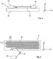
- the schematic view of Fig. 1 shows a first embodiment of a DCB substrate 10 according to the invention.
- the invention will be described exemplarily on the basis of a DCB substrate.
- the invention can also be used for manufacturing different kinds of metal-ceramic substrates so that the following description can be applied to different kinds of substrates.
- the substrate can be an AMB substrate with copper layer(s) or an DAB substrate with aluminium layer(s).
- one or more metal layers are applied to a central ceramic insulation layer and at least one trimmed resistor is formed in at least one metal layer.
- the metal-ceramic substrate 10 shown in Fig. 1 comprises a central ceramic insulation layer 20 which has a rectangular shape.
- a top conductive copper layer has been applied to the top surface of the insulation layer 20 by a common DCB process for bonding copper directly to the central insulation layer 20.
- the copper layer consists of two rectangular layer regions 32 and 33, and a web or narrow band connecting the two layer regions 32, 33. This web forms an ablation area 31 in which the thickness of the copper is reduced compared to the two layer regions 32 and 33.
- the thickness of the copper layer in the ablation area 31 is smaller than in the layer regions 32 and 33, which has been achieved by laser ablation with ultrashort pulses in the z-axis.
- More than one ablation area can be defined on a copper layer, and top and/or bottom copper layers can be trimmed on an insulation layer 20. Furthermore, the ablation area and adjacent layer regions can have different shapes.
- the invention is not limited to a DCB substrate according to Fig. 1 since this schematic top view only serves for illustrating the principles of the invention.
- the ablation area 31 has a length l in the x-axis and a width w in the y-axis.
- the starting thickness H of the top copper layer 30 basically corresponds to the thickness of the adjacent layer regions 32, 33, as can be seen in the schematic side view of Fig. 2.
- Fig. 2 shows a DCB substrate 10 before trimming of the ablation area 31.
- the length I and the cross-section A w*H of the ablation area 31 lead to a certain starting value for the electrical resistivity.
- the electrical resistivity of the copper layer 30 in the ablation area 31 is reduced by reducing the thickness H of the ablation area 31.
- the width w of the ablation area 31 can also be reduced by laser ablation in order to increase the reduction of the cross-section A. Consequently, the width w of the ablation area 31 in Fig. 1 has been produced by etching or by laser trimming.
- Fig. 3 shows a schematic side view of the resulting DCB substrate 10 after trimming, i.e. after reduction of the thickness of the copper layer 30 to a certain value h. The difference H h is the thickness reduction by laser ablation.
- the width w of the original ablation area is defined by the original layout from etching of the conductive copper layer.
- the length l is always 1 mm.
- the width w can be reduced and/or the length l of an ablation area can be increased. This is shown in the exemplary embodiments 5-7 and can also be achieved by laser trimming, whereby a full cut is used from the top to the bottom of the top copper surface 30.
- the width w is reduced to 0.1 mm, for example by laser ablation and the length l is kept at 1 mm. With a thickness reduction of 0.295 mm, this results in a cross-section A of 0.0005 mm 2 and a resistance value of 34.4200 Ohm.
- the same width w and the same thickness reduction of the ablation area lead to a resistance value of 172.1000 Ohm (embodiment 6).
- a high resistance value of 1,376.8000 Ohm can be achieved with a thickness reduction of 0.295 mm.
- the width w and/or the length l is trimmed before the thickness of the ablation area is reduced by laser ablation to the final value.
- the laser ablation of an ablation area 31 is performed with a series of discrete ultrashort single laser pulses which remove material from the ablation area which reduces the thickness of a copper layer in this ablation area.
- the resulting resistivity is simultaneously measured and ablation is terminated once a target resistivity value is reached.
- laser ablation of an ablation area 31 is performed with a scanning ablation. Thereby, the laser beam is deflected from pulse to pulse and this deflection from pulse to pulse is minimized in order to maximize pulse frequency and process speed.
- Fig. 4 shows a schematic top view on an ablation area 31 during raster scanning which is used to explain the basic principle of raster scanning.
- Laser beams from a laser device 40 are deflected by a deflection system 41, e.g. a galvanometer scan system.
- the laser beams are focused and guided to the ablation area 31 in order to form laser spots 42 which run in rectangular patterns consisting of several parallel lines. With an increasing number of raster scans in the ablation area, the depth of the irradiated area increases.
- the diameter of the laser spots 42 is between 20 and 30 ⁇ m.
Landscapes
- Engineering & Computer Science (AREA)
- Optics & Photonics (AREA)
- Physics & Mathematics (AREA)
- Plasma & Fusion (AREA)
- Mechanical Engineering (AREA)
- Chemical & Material Sciences (AREA)
- Microelectronics & Electronic Packaging (AREA)
- Ceramic Engineering (AREA)
- Manufacturing & Machinery (AREA)
- Inorganic Chemistry (AREA)
- Materials Engineering (AREA)
- Structural Engineering (AREA)
- Organic Chemistry (AREA)
- Apparatuses And Processes For Manufacturing Resistors (AREA)
- Laser Beam Processing (AREA)
- Manufacturing Of Printed Wiring (AREA)
Abstract
Description
- The invention relates to a method for manufacturing a metal-ceramic substrate according to the preamble of Claim 1, including providing a central ceramic insulation layer with a conductive metal layer on one or both of its surfaces. The invention also relates to a corresponding metal-ceramic substrate which has been manufactured by such method.
- Metal-ceramic substrates or ceramic substrates with metallizations are known as substrates for electrical and electronic circuits or modules, especially for high-power modules. Thereby, a metal can be applied to a ceramic substrate by Active-Metal-Brazing (AMB) or Direct-Aluminium-Bonding (DAB), for example. The power and current carrying capabilities of power switches are commonly limited by their package, because the package introduces thermal and electrical resistivity that can cause power loss and corresponding heating of the semiconductor die beyond its specified limits. Therefore, high power packages often use substrates like Direct-Bonded-Copper (DBC). A DBC substrate is a structure which provides for a low thermal resistivity, a very good thermal conductivity and a very good thermal cycling stability. A DBC substrate generally comprises a central insulation layer, which has top and bottom conductive copper layers on its top and bottom surfaces. These are frequently copper. The central insulation layer may be a ceramic material like aluminium-oxide or aluminium nitride.
- Certain resistances are achieved on metal-ceramic substrates, for example shunt resistors or gate resistors. Typically, separate passive components are used to achieve these resistances. In the field of thick-film resistors it is known to trim resistors in order to set a required resistivity value. For example, specially printed resistivity paste is fired and cut while simultaneously monitoring the resistivity value. Thereby, single cuts, double cuts or L-cuts can be used, for example. All kinds of ablative processes can be used to apply the cuts, though commonly laser ablation emerged as a method of choice. Common to these trimmings is that a side cut is always performed from the top to the bottom, which means that a full cut is applied in the z-axis while the remaining resistor thickness remains at 100% of the starting resistivity.
- However, unlike thick film, substrates for high voltage are not easily suitable for trimming. Conventional laser systems carry the risk to damage the isolator and/or induce cracks during trimming which later lead to failure in thermal cycling. That is why there is a need for a solution to implement trimming on the substrate level and to eliminate a separate resistor.
- According to the invention, this object is achieved with a method for manufacturing a metal-ceramic substrate according to the independent Claim 1. Advantageous embodiments of the method result from dependent Claims 2-8. The object is also achieved by a metal-ceramic substrate according to the independent Claim 9. Advantageous further developments are disclosed in Claims 10-13.
- It should be noted that the characteristics mentioned individually in the claims can be combined with each other in any technically appropriate manner producing further embodiments of the invention. The description also characterizes and specifies the invention especially in connection with the figures.
- The method according to the invention is used for manufacturing a metal-ceramic substrate. This metal-ceramic substrate can be an AMB substrate (Active-Metal-Brazing) or a DAB substrate (Direct-Aluminium-Bonding), for example. In one embodiment of the invention, it is a DCB substrate which is a so-called Direct-Copper-Bonding substrate which is also known as DBC substrate (Direct Bond Copper). DCB substrates are suited to high power applications that demand a high level of heat dissipation. Thus, the DCB substrate is a high power substrate. Thereby, a central ceramic insulation layer is provided with a conductive metal layer on one or both of its surfaces. In case the conductive metal layer is made of copper, this copper is applied to the central ceramic insulation layer by means of a DCB process. The central insulation layer is a ceramic layer like an alumina layer made of AL2O3 or aluminium nitride, for example. Alternatively, beryllium oxide (BeO) can be used. A sheet of copper is commonly bonded to one or both sides of this central insulation layer by a high-temperature oxidation process. An electrical circuit is formed at least in a top copper layer by preforming, firing and/or chemical etching. A bottom copper layer can be kept plain. However, the invention can be used for manufacturing substrates with different kinds of metal layers. For example, it could also be used for ceramic substrates with conductive metal layers made of aluminium instead of copper. In addition to AL2O3, AIN and BeO, silicon nitride (Si3N4) or similar ceramic materials can be used to form the central ceramic insulation layer.
- According to the invention, laser ablation with an ultrashort pulse laser is performed locally on at least one conductive metal layer within a certain ablation area. This laser ablation is performed until a certain resistivity of the conductive metal layer is achieved in this ablation area, whereby the thickness of the conductive metal layer in the ablation area is reduced to a value above zero. The metal layer is ablated in the z-axis which is orthogonal to the surface of the central ceramic insulation layer. Thus, the metal layer is trimmed by reducing its thickness in a certain ablation area, but the metal layer is not fully removed by laser ablation in this region. This z-axis trimming can be performed on one or both metal layers of a substrate. If more than one metal layer is trimmed, an ablation area is defined for each metal layer. Further, more than one ablation area can be defined in a metal layer.
- The ablation consists of a series of discrete single laser pulses which remove material from the ablation area. Thereby, the cross-section of the metal layer is reduced in the ablation area, which increases the electrical resistivity in this area. With this method, certain resistance values can be achieved in a metal layer of a metal-ceramic substrate to form resistors like shunt resistors or gate resistors, for example. Thereby, no separate passive components are needed, which saves material and manufacturing time. In addition, the required resistance values can be adjusted very precisely. Thus, the invention allows to implement trimming on the substrate level and to eliminate separate resistors.
- With oxygen-free copper, for example, electrical resistance values from about 1 mOhm to 1 kOhm can be achieved, whereby large resistance values can require further measures. For large electrical resistance values, the z-axis trimming can be combined with a known side cut, for example. Thus, in one embodiment of the invention, in addition to the trimming steps at least one full cut is produced across the thickness of the conductive metal layer which locally reduces said thickness to zero in the ablation area. Thus, the width of the ablation area is reduced by a full side cut and its thickness is reduced by a partial ablation, which results in a significantly reduced cross-section.
- Preferably, the resistivity of the conductive metal layer is measured during the laser ablation, and the laser ablation is performed until a target value of resistivity is reached. Thus, the resistivity value is monitored simultaneously during laser ablation so that the resistivity can be adjusted very precisely.
- The use of ultrashort pulse lasers is advantageous, because its ultrashort duration prevents thermal degradation of the to-be-ablated base material and enables an extremely precise cut. Especially the processing of copper using ultrashort pulses provides for a very precise ablation and high removal rates. Thereby, the duration of the pulse preferably ranges between 200 fs and 10 ps. In one embodiment of the invention, laser beams are raster scanned across the ablation area to perform a scanning ablation. This means that laser beams are guided to the metal surface in rectangular patterns consisting of overlapping parallel lines, for example. With an increasing number of raster scans in the ablation area, the depth of the irradiated area increases. Thereby, the laser beams are deflected and focused. For example, a galvanometer scan system is used to deflect the laser beams, and an objective is used to focus the laser beams to focus spots with diameters in the range of about 20 to 30 µm.
- The laser parameters are chosen to meet specific requirements. In particular, the laser parameters are chosen to achieve high material removal rates. For example, the laser ablation is performed with a pulse repetition frequency fR in the range of 1 to 20 MHz, in particular in the range of 6 to 7 MHz. Further, the laser ablation is performed with a pulse energy QSP in the range of 1 to 50 µJ, in particular in the range of 4 to 6 µJ. Preferably, a wavelength is used that optimizes absorption in the metal layer, while minimizing absorption of the ceramic insulation layer. The wavelength can be chosen about 1026 nm or 1030 nm, for example. High material removal rates can be found with pulses of about 5 µJ energy at about 6.5 MHz repetition frequency, for example. In one embodiment of the invention, the thickness of a metal layer on a substrate is between 0.2 to 0.5 mm, in particular about 0.3 mm. With this starting thickness of about 0.3 mm, a thickness reduction by means of the laser ablation between 0.1 and 0.295 mm is performed.
- The invention also covers a corresponding metal-ceramic substrate, including a central ceramic insulation layer with a conductive metal layer on one or both of its surfaces. In one embodiment of the invention the conductive metal layer is made of copper which is applied to the central ceramic insulation layer by means of a DCB process. Within an ablation area the thickness of the conductive metal layer is reduced compared to adjacent regions, whereby said thickness is reduced to a value above zero. This metal-ceramic substrate can be manufactured with a method according to an embodiment of the method according to the invention. For example, in addition to a reduction of thickness to a value above zero, the conductive metal layer can comprise at least one full cut across the thickness which locally reduces said thickness to zero in the ablation area. For example, a DCB substrate with a standard side cut can be provided with a copper layer with a large local resistance, in particular with local resistance values between 34 and 1,400 Ohm.
- In one embodiment of the invention, an ablation area in the conductive metal layer is defined by a web or band between two layer regions of metal. On a DCB substrate, this web is produced by etching after the DCB process, for example.
- Other advantages, special features and useful further developments of the invention result from the dependent claims and the preferred embodiments shown below by means of the figures, where
- Fig. 1
- shows a schematic top view on a DCB substrate according to an embodiment of the invention;
- Fig. 2
- shows a schematic side view of the substrate of
Fig. 1 before trimming; - Fig. 3
- shows the substrate of
Fig. 2 after trimming; and - Fig. 4
- shows a schematic top view on an ablation area during raster scanning.
- The schematic view of
Fig. 1 shows a first embodiment of aDCB substrate 10 according to the invention. The invention will be described exemplarily on the basis of a DCB substrate. However, the invention can also be used for manufacturing different kinds of metal-ceramic substrates so that the following description can be applied to different kinds of substrates. For example, the substrate can be an AMB substrate with copper layer(s) or an DAB substrate with aluminium layer(s). In any case, one or more metal layers are applied to a central ceramic insulation layer and at least one trimmed resistor is formed in at least one metal layer. - The metal-
ceramic substrate 10 shown inFig. 1 comprises a centralceramic insulation layer 20 which has a rectangular shape. A top conductive copper layer has been applied to the top surface of theinsulation layer 20 by a common DCB process for bonding copper directly to thecentral insulation layer 20. In this embodiment, the copper layer consists of tworectangular layer regions layer regions ablation area 31 in which the thickness of the copper is reduced compared to the twolayer regions ablation area 31 is smaller than in thelayer regions - More than one ablation area can be defined on a copper layer, and top and/or bottom copper layers can be trimmed on an
insulation layer 20. Furthermore, the ablation area and adjacent layer regions can have different shapes. Thus, the invention is not limited to a DCB substrate according toFig. 1 since this schematic top view only serves for illustrating the principles of the invention. - The
ablation area 31 has a length l in the x-axis and a width w in the y-axis. Before trimming of theablation area 31 in the z-axis, the starting thickness H of thetop copper layer 30 basically corresponds to the thickness of theadjacent layer regions Fig. 2. Fig. 2 shows aDCB substrate 10 before trimming of theablation area 31. The length I and the cross-section A = w*H of theablation area 31 lead to a certain starting value for the electrical resistivity. Thereby, the electrical resistivity of oxygen-free copper is = 0.01721 Ohm mm2/m, which means that the electrical resistance R = 0.01721 Ohm mm2/m * l/ (w*H) for theablation area 31. With a constant length l and a constant width w of theablation area 31, the electrical resistivity of thecopper layer 30 in theablation area 31 is reduced by reducing the thickness H of theablation area 31. - Optionally, the width w of the
ablation area 31 can also be reduced by laser ablation in order to increase the reduction of the cross-section A. Consequently, the width w of theablation area 31 inFig. 1 has been produced by etching or by laser trimming.Fig. 3 shows a schematic side view of the resultingDCB substrate 10 after trimming, i.e. after reduction of the thickness of thecopper layer 30 to a certain value h. The difference H h is the thickness reduction by laser ablation. - With a starting thickness H = 0.3 mm, the following electrical resistances can be achieved for seven exemplary embodiments of a DCB substrate according to the invention:
Width w of original ablation area [mm] Length I of original ablation area [mm] Thickness reduction H-h [mm] Resulting cross-section A [mm2] Electrical resistance [Ohm] 1 1 1 0.1 0.2 0.0861 2 5 1 0.1 1 0.0172 3 10 1 0.1 2 0.0086 4 0.7 1 0.295 0.0035 4.9171 5 0.1 1 0.295 0.0005 34.4200 6 0.1 5 0.295 0.0005 172.1000 7 0.05 20 0.295 0.00025 1,376.8000 - In embodiments 1-4, the width w of the original ablation area is defined by the original layout from etching of the conductive copper layer. The length l is always 1 mm. By thickness reductions between 0.1 and 0.295 mm the resulting cross section A = w*h is between 0.2 and 0.0035. This results in electrical resistance values in the trimmed ablation area between 0.0861 and 4.9171 Ohm.
- For larger resistance values, the width w can be reduced and/or the length l of an ablation area can be increased. This is shown in the exemplary embodiments 5-7 and can also be achieved by laser trimming, whereby a full cut is used from the top to the bottom of the
top copper surface 30. In embodiment 5, the width w is reduced to 0.1 mm, for example by laser ablation and the length l is kept at 1 mm. With a thickness reduction of 0.295 mm, this results in a cross-section A of 0.0005 mm2 and a resistance value of 34.4200 Ohm. With an increased length l, the same width w and the same thickness reduction of the ablation area lead to a resistance value of 172.1000 Ohm (embodiment 6). If the width w is further reduced and the length l of the ablation area is further increased like in embodiment 7, a high resistance value of 1,376.8000 Ohm can be achieved with a thickness reduction of 0.295 mm. Preferably, the width w and/or the length l is trimmed before the thickness of the ablation area is reduced by laser ablation to the final value. - The laser ablation of an
ablation area 31 is performed with a series of discrete ultrashort single laser pulses which remove material from the ablation area which reduces the thickness of a copper layer in this ablation area. The resulting resistivity is simultaneously measured and ablation is terminated once a target resistivity value is reached. Preferably, laser ablation of anablation area 31 is performed with a scanning ablation. Thereby, the laser beam is deflected from pulse to pulse and this deflection from pulse to pulse is minimized in order to maximize pulse frequency and process speed.Fig. 4 shows a schematic top view on anablation area 31 during raster scanning which is used to explain the basic principle of raster scanning. Laser beams from alaser device 40 are deflected by adeflection system 41, e.g. a galvanometer scan system. The laser beams are focused and guided to theablation area 31 in order to form laser spots 42 which run in rectangular patterns consisting of several parallel lines. With an increasing number of raster scans in the ablation area, the depth of the irradiated area increases. The diameter of the laser spots 42 is between 20 and 30 µm. The spacing between lines of laser spots 42 is the hatch distance xH, whereas the distance between the laser spots 42 along a line is defined by the pulse spacing xp. This pulse spacing depends on the scan speed vs or the pulse repetition frequency fR or both (vs = xH * fR). -
- 10,10
- substrate, DCB substrate
- 20
- insulation layer
- 30
- top conductive copper layer
- 31
- ablation area
- 32,33
- layer region
- 40
- laser device
- 41
- deflection system
- 42
- laser spot
- w
- width
- l
- length
- H
- starting thickness
- h
- reduced thickness
- xp
- pulse spacing
- xH
- hatch distance
- vs
- scan speed
Claims (13)
- A method for manufacturing a metal-ceramic substrate (10), including providing a central ceramic insulation layer (20) with a conductive metal layer (30) on one or both of its surfaces,
characterized in that laser ablation with an ultrashort pulse laser is performed on at least one conductive metal layer (30) locally within an ablation area (31) until a certain resistivity of the conductive metal layer (30) is achieved in this ablation area (31), whereby the thickness of the conductive metal layer (30) in the ablation area (31) is reduced to a value above zero. - The method according to Claim 1,
characterized in that in addition to the steps of Claim 1 at least one full cut is produced across the thickness of the conductive metal layer (30) which locally reduces said thickness to zero in the ablation area (31). - The method according to Claim 1 or 2,
characterized in that the resistivity of the conductive metal layer (30) is measured during the laser ablation and the laser ablation is performed until a target value of resistivity is reached. - The method according to one of Claims 1 to 3,
characterized in that laser beams are raster scanned across the ablation area (31) to perform a scanning ablation. - The method according to one of Claims 1 to 4,
characterized in that the laser ablation is performed with a pulse repetition frequency between 1 to 20 MHz. - The method according to one of Claims 1 to 5,
characterized in that the laser ablation is performed with a pulse energy between 1 and 50 µJ. - The method according to one of Claims 1 to 6,
characterized in that the starting thickness of the conductive metal layer (30) in the ablation area (31) is about 0.3 mm, and the thickness reduction by means of the laser ablation is between 0.1 and 0.295 mm. - The method according to one of Claims 1 to 7,
characterized in that the conductive metal layer (30) is made of copper which is applied to the central ceramic insulation layer (20) by means of a DCB process. - Metal-ceramic substrate (10), including a central ceramic insulation layer (20) with a conductive metal layer (30) on one or both of its surfaces,
characterized in that within an ablation area (31) the thickness of the conductive metal layer (30) is reduced compared to adjacent regions, whereby said thickness is reduced to a value above zero. - The substrate according to Claim 9,
characterized in that in addition to a reduction of thickness to a value above zero the conductive metal layer (30) comprises at least one full cut across the thickness which locally reduces said thickness to zero in the ablation area (31). - The substrate according to Claim 9 or 10,
characterized in that the metal-ceramic substrate (10) is manufactured with a method according one of Claims 1 to 8. - The substrate according to one of Claims 9 to 11,
characterized in that an ablation area (31) in the conductive metal layer (30) is defined by a web between two layer regions (32;33) of metal. - Metal-ceramic substrate (10) according to one of Claims 9 to 12,
characterized in that the conductive metal layer (30) is made of copper which has been applied to the central ceramic insulation layer (20) by means of a DCB process.
Priority Applications (1)
| Application Number | Priority Date | Filing Date | Title |
|---|---|---|---|
| EP17190803.1A EP3456698B1 (en) | 2017-09-13 | 2017-09-13 | Method for manufacturing metal-ceramic substrate with trimmed resistors |
Applications Claiming Priority (1)
| Application Number | Priority Date | Filing Date | Title |
|---|---|---|---|
| EP17190803.1A EP3456698B1 (en) | 2017-09-13 | 2017-09-13 | Method for manufacturing metal-ceramic substrate with trimmed resistors |
Publications (2)
| Publication Number | Publication Date |
|---|---|
| EP3456698A1 true EP3456698A1 (en) | 2019-03-20 |
| EP3456698B1 EP3456698B1 (en) | 2022-11-16 |
Family
ID=59895109
Family Applications (1)
| Application Number | Title | Priority Date | Filing Date |
|---|---|---|---|
| EP17190803.1A Active EP3456698B1 (en) | 2017-09-13 | 2017-09-13 | Method for manufacturing metal-ceramic substrate with trimmed resistors |
Country Status (1)
| Country | Link |
|---|---|
| EP (1) | EP3456698B1 (en) |
Cited By (1)
| Publication number | Priority date | Publication date | Assignee | Title |
|---|---|---|---|---|
| WO2024017494A1 (en) * | 2022-07-19 | 2024-01-25 | Oerlikon Metco Ag, Wohlen | Electric heating element production method |
Citations (4)
| Publication number | Priority date | Publication date | Assignee | Title |
|---|---|---|---|---|
| US20040009618A1 (en) * | 2002-03-27 | 2004-01-15 | Couch Bruce L. | Method and system for high-speed, precise micromachining an array of devices |
| US20060055504A1 (en) * | 2004-09-13 | 2006-03-16 | Pailthorp Robert M | Measurement extrapolation technique to compensate for thermal EMF generated during laser trimming |
| DE102012206973A1 (en) * | 2012-04-26 | 2013-10-31 | Osram Gmbh | Method for producing conductor tracks in copper layer of substrate e.g. direct copper bonded (DCB) substrate used for mounting LED in LED module, involves forming copper layer with specific region having reduced thickness |
| DE102013102540A1 (en) * | 2013-02-22 | 2014-08-28 | Curamik Electronics Gmbh | Metal-ceramic substrate, module arrangement and method for producing a metal-ceramic substrate |
Family Cites Families (1)
| Publication number | Priority date | Publication date | Assignee | Title |
|---|---|---|---|---|
| JPH1032110A (en) * | 1996-07-16 | 1998-02-03 | Matsushita Refrig Co Ltd | Laser-trimming method for thick-film resistor |
-
2017
- 2017-09-13 EP EP17190803.1A patent/EP3456698B1/en active Active
Patent Citations (4)
| Publication number | Priority date | Publication date | Assignee | Title |
|---|---|---|---|---|
| US20040009618A1 (en) * | 2002-03-27 | 2004-01-15 | Couch Bruce L. | Method and system for high-speed, precise micromachining an array of devices |
| US20060055504A1 (en) * | 2004-09-13 | 2006-03-16 | Pailthorp Robert M | Measurement extrapolation technique to compensate for thermal EMF generated during laser trimming |
| DE102012206973A1 (en) * | 2012-04-26 | 2013-10-31 | Osram Gmbh | Method for producing conductor tracks in copper layer of substrate e.g. direct copper bonded (DCB) substrate used for mounting LED in LED module, involves forming copper layer with specific region having reduced thickness |
| DE102013102540A1 (en) * | 2013-02-22 | 2014-08-28 | Curamik Electronics Gmbh | Metal-ceramic substrate, module arrangement and method for producing a metal-ceramic substrate |
Cited By (1)
| Publication number | Priority date | Publication date | Assignee | Title |
|---|---|---|---|---|
| WO2024017494A1 (en) * | 2022-07-19 | 2024-01-25 | Oerlikon Metco Ag, Wohlen | Electric heating element production method |
Also Published As
| Publication number | Publication date |
|---|---|
| EP3456698B1 (en) | 2022-11-16 |
Similar Documents
| Publication | Publication Date | Title |
|---|---|---|
| US9190235B2 (en) | Manufacturability of SMD and through-hole fuses using laser process | |
| US20050062583A1 (en) | Drift-sensitive laser trimming of circuit elements | |
| KR20060030903A (en) | How to form scribe lines on passive electronic component substrates | |
| US20240178098A1 (en) | Method for producing a metal-ceramic substrate, and metal-ceramic substrate produced using a method of this type | |
| CN115517026A (en) | Carrier substrate and method for manufacturing carrier substrate | |
| EP3615259B1 (en) | Method of laser ablation of a metal-ceramic substrate | |
| EP0895284B1 (en) | Process for manufacturing metal-ceramic composite circuit substrates | |
| EP1470743B1 (en) | Power module | |
| WO2014190968A1 (en) | Metal-ceramic substrate and method for producing a metal-ceramic substrate | |
| EP3456698B1 (en) | Method for manufacturing metal-ceramic substrate with trimmed resistors | |
| EP3682474B1 (en) | Arrangement of several adapter elements and method for producing such a composite | |
| KR100894025B1 (en) | Method for Resistor Trimming Using Small Uniform Spots from Solid-State Fin Lasers | |
| EP2856586B1 (en) | Laser ablation process for manufacturing submounts for laser diode and laser diode units | |
| EP4266835B1 (en) | Ceramic scribe substrate, method for manufacturing ceramic scribe substrate, method for manufacturing ceramic substrate, method for manufacturing ceramic circuit board, and method for manufacturing semiconductor elements | |
| EP3761351B1 (en) | Insulated circuit board | |
| JP5318600B2 (en) | Manufacturing method of multilayer ceramic electronic component | |
| US20240332123A1 (en) | Scribed ceramic circuit substrate, ceramic circuit substrate, method for producing scribed ceramic circuit substrate, method for producing ceramic circuit substrate, and method for producing semiconductor device | |
| US4719443A (en) | Low capacitance power resistor using beryllia dielectric heat sink layer and low toxicity method for its manufacture | |
| DE4017181A1 (en) | ELECTRICAL COMPONENT | |
| KR20060098370A (en) | Laser-based Passive Electronic Device Cutting | |
| KR101929613B1 (en) | Ceramic circuit board and method of manufacturing the same | |
| JP2004311691A (en) | Metal plate for circuit and ceramic circuit board | |
| WO2006127436A1 (en) | Method of forming passive electronic components on a substrate by direct write technique using shaped uniform laser beam | |
| JP7693951B2 (en) | Ceramic substrate, ceramic circuit board, semiconductor device, method for manufacturing ceramic substrate, and method for manufacturing divided ceramic substrate | |
| JP2001118705A (en) | Chip resistor |
Legal Events
| Date | Code | Title | Description |
|---|---|---|---|
| PUAI | Public reference made under article 153(3) epc to a published international application that has entered the european phase |
Free format text: ORIGINAL CODE: 0009012 |
|
| STAA | Information on the status of an ep patent application or granted ep patent |
Free format text: STATUS: THE APPLICATION HAS BEEN PUBLISHED |
|
| AK | Designated contracting states |
Kind code of ref document: A1 Designated state(s): AL AT BE BG CH CY CZ DE DK EE ES FI FR GB GR HR HU IE IS IT LI LT LU LV MC MK MT NL NO PL PT RO RS SE SI SK SM TR |
|
| AX | Request for extension of the european patent |
Extension state: BA ME |
|
| STAA | Information on the status of an ep patent application or granted ep patent |
Free format text: STATUS: REQUEST FOR EXAMINATION WAS MADE |
|
| 17P | Request for examination filed |
Effective date: 20190830 |
|
| RBV | Designated contracting states (corrected) |
Designated state(s): AL AT BE BG CH CY CZ DE DK EE ES FI FR GB GR HR HU IE IS IT LI LT LU LV MC MK MT NL NO PL PT RO RS SE SI SK SM TR |
|
| STAA | Information on the status of an ep patent application or granted ep patent |
Free format text: STATUS: EXAMINATION IS IN PROGRESS |
|
| 17Q | First examination report despatched |
Effective date: 20201218 |
|
| GRAP | Despatch of communication of intention to grant a patent |
Free format text: ORIGINAL CODE: EPIDOSNIGR1 |
|
| STAA | Information on the status of an ep patent application or granted ep patent |
Free format text: STATUS: GRANT OF PATENT IS INTENDED |
|
| RIC1 | Information provided on ipc code assigned before grant |
Ipc: B23K 103/12 20060101ALI20220523BHEP Ipc: B23K 101/38 20060101ALI20220523BHEP Ipc: B23K 26/40 20140101ALI20220523BHEP Ipc: B23K 26/361 20140101ALI20220523BHEP Ipc: B23K 26/082 20140101ALI20220523BHEP Ipc: B23K 26/00 20140101ALI20220523BHEP Ipc: H05K 1/02 20060101ALI20220523BHEP Ipc: H05K 1/03 20060101ALI20220523BHEP Ipc: H05K 1/16 20060101ALI20220523BHEP Ipc: H05K 3/02 20060101ALI20220523BHEP Ipc: B23K 26/03 20060101ALI20220523BHEP Ipc: H01C 17/242 20060101ALI20220523BHEP Ipc: H01L 49/02 20060101ALI20220523BHEP Ipc: B23K 26/351 20140101ALI20220523BHEP Ipc: B23K 26/0622 20140101ALI20220523BHEP Ipc: C04B 37/02 20060101AFI20220523BHEP |
|
| INTG | Intention to grant announced |
Effective date: 20220629 |
|
| GRAS | Grant fee paid |
Free format text: ORIGINAL CODE: EPIDOSNIGR3 |
|
| GRAA | (expected) grant |
Free format text: ORIGINAL CODE: 0009210 |
|
| STAA | Information on the status of an ep patent application or granted ep patent |
Free format text: STATUS: THE PATENT HAS BEEN GRANTED |
|
| AK | Designated contracting states |
Kind code of ref document: B1 Designated state(s): AL AT BE BG CH CY CZ DE DK EE ES FI FR GB GR HR HU IE IS IT LI LT LU LV MC MK MT NL NO PL PT RO RS SE SI SK SM TR |
|
| REG | Reference to a national code |
Ref country code: GB Ref legal event code: FG4D |
|
| REG | Reference to a national code |
Ref country code: CH Ref legal event code: EP |
|
| REG | Reference to a national code |
Ref country code: IE Ref legal event code: FG4D |
|
| REG | Reference to a national code |
Ref country code: DE Ref legal event code: R096 Ref document number: 602017063681 Country of ref document: DE |
|
| REG | Reference to a national code |
Ref country code: AT Ref legal event code: REF Ref document number: 1531707 Country of ref document: AT Kind code of ref document: T Effective date: 20221215 |
|
| REG | Reference to a national code |
Ref country code: LT Ref legal event code: MG9D |
|
| REG | Reference to a national code |
Ref country code: NL Ref legal event code: MP Effective date: 20221116 |
|
| REG | Reference to a national code |
Ref country code: AT Ref legal event code: MK05 Ref document number: 1531707 Country of ref document: AT Kind code of ref document: T Effective date: 20221116 |
|
| PG25 | Lapsed in a contracting state [announced via postgrant information from national office to epo] |
Ref country code: SE Free format text: LAPSE BECAUSE OF FAILURE TO SUBMIT A TRANSLATION OF THE DESCRIPTION OR TO PAY THE FEE WITHIN THE PRESCRIBED TIME-LIMIT Effective date: 20221116 Ref country code: PT Free format text: LAPSE BECAUSE OF FAILURE TO SUBMIT A TRANSLATION OF THE DESCRIPTION OR TO PAY THE FEE WITHIN THE PRESCRIBED TIME-LIMIT Effective date: 20230316 Ref country code: NO Free format text: LAPSE BECAUSE OF FAILURE TO SUBMIT A TRANSLATION OF THE DESCRIPTION OR TO PAY THE FEE WITHIN THE PRESCRIBED TIME-LIMIT Effective date: 20230216 Ref country code: LT Free format text: LAPSE BECAUSE OF FAILURE TO SUBMIT A TRANSLATION OF THE DESCRIPTION OR TO PAY THE FEE WITHIN THE PRESCRIBED TIME-LIMIT Effective date: 20221116 Ref country code: FI Free format text: LAPSE BECAUSE OF FAILURE TO SUBMIT A TRANSLATION OF THE DESCRIPTION OR TO PAY THE FEE WITHIN THE PRESCRIBED TIME-LIMIT Effective date: 20221116 Ref country code: ES Free format text: LAPSE BECAUSE OF FAILURE TO SUBMIT A TRANSLATION OF THE DESCRIPTION OR TO PAY THE FEE WITHIN THE PRESCRIBED TIME-LIMIT Effective date: 20221116 Ref country code: AT Free format text: LAPSE BECAUSE OF FAILURE TO SUBMIT A TRANSLATION OF THE DESCRIPTION OR TO PAY THE FEE WITHIN THE PRESCRIBED TIME-LIMIT Effective date: 20221116 |
|
| PG25 | Lapsed in a contracting state [announced via postgrant information from national office to epo] |
Ref country code: RS Free format text: LAPSE BECAUSE OF FAILURE TO SUBMIT A TRANSLATION OF THE DESCRIPTION OR TO PAY THE FEE WITHIN THE PRESCRIBED TIME-LIMIT Effective date: 20221116 Ref country code: PL Free format text: LAPSE BECAUSE OF FAILURE TO SUBMIT A TRANSLATION OF THE DESCRIPTION OR TO PAY THE FEE WITHIN THE PRESCRIBED TIME-LIMIT Effective date: 20221116 Ref country code: LV Free format text: LAPSE BECAUSE OF FAILURE TO SUBMIT A TRANSLATION OF THE DESCRIPTION OR TO PAY THE FEE WITHIN THE PRESCRIBED TIME-LIMIT Effective date: 20221116 Ref country code: IS Free format text: LAPSE BECAUSE OF FAILURE TO SUBMIT A TRANSLATION OF THE DESCRIPTION OR TO PAY THE FEE WITHIN THE PRESCRIBED TIME-LIMIT Effective date: 20230316 Ref country code: HR Free format text: LAPSE BECAUSE OF FAILURE TO SUBMIT A TRANSLATION OF THE DESCRIPTION OR TO PAY THE FEE WITHIN THE PRESCRIBED TIME-LIMIT Effective date: 20221116 Ref country code: GR Free format text: LAPSE BECAUSE OF FAILURE TO SUBMIT A TRANSLATION OF THE DESCRIPTION OR TO PAY THE FEE WITHIN THE PRESCRIBED TIME-LIMIT Effective date: 20230217 |
|
| PG25 | Lapsed in a contracting state [announced via postgrant information from national office to epo] |
Ref country code: NL Free format text: LAPSE BECAUSE OF FAILURE TO SUBMIT A TRANSLATION OF THE DESCRIPTION OR TO PAY THE FEE WITHIN THE PRESCRIBED TIME-LIMIT Effective date: 20221116 |
|
| P01 | Opt-out of the competence of the unified patent court (upc) registered |
Effective date: 20230528 |
|
| PG25 | Lapsed in a contracting state [announced via postgrant information from national office to epo] |
Ref country code: SM Free format text: LAPSE BECAUSE OF FAILURE TO SUBMIT A TRANSLATION OF THE DESCRIPTION OR TO PAY THE FEE WITHIN THE PRESCRIBED TIME-LIMIT Effective date: 20221116 Ref country code: RO Free format text: LAPSE BECAUSE OF FAILURE TO SUBMIT A TRANSLATION OF THE DESCRIPTION OR TO PAY THE FEE WITHIN THE PRESCRIBED TIME-LIMIT Effective date: 20221116 Ref country code: EE Free format text: LAPSE BECAUSE OF FAILURE TO SUBMIT A TRANSLATION OF THE DESCRIPTION OR TO PAY THE FEE WITHIN THE PRESCRIBED TIME-LIMIT Effective date: 20221116 Ref country code: DK Free format text: LAPSE BECAUSE OF FAILURE TO SUBMIT A TRANSLATION OF THE DESCRIPTION OR TO PAY THE FEE WITHIN THE PRESCRIBED TIME-LIMIT Effective date: 20221116 Ref country code: CZ Free format text: LAPSE BECAUSE OF FAILURE TO SUBMIT A TRANSLATION OF THE DESCRIPTION OR TO PAY THE FEE WITHIN THE PRESCRIBED TIME-LIMIT Effective date: 20221116 |
|
| REG | Reference to a national code |
Ref country code: DE Ref legal event code: R097 Ref document number: 602017063681 Country of ref document: DE |
|
| PG25 | Lapsed in a contracting state [announced via postgrant information from national office to epo] |
Ref country code: SK Free format text: LAPSE BECAUSE OF FAILURE TO SUBMIT A TRANSLATION OF THE DESCRIPTION OR TO PAY THE FEE WITHIN THE PRESCRIBED TIME-LIMIT Effective date: 20221116 Ref country code: AL Free format text: LAPSE BECAUSE OF FAILURE TO SUBMIT A TRANSLATION OF THE DESCRIPTION OR TO PAY THE FEE WITHIN THE PRESCRIBED TIME-LIMIT Effective date: 20221116 |
|
| PLBE | No opposition filed within time limit |
Free format text: ORIGINAL CODE: 0009261 |
|
| STAA | Information on the status of an ep patent application or granted ep patent |
Free format text: STATUS: NO OPPOSITION FILED WITHIN TIME LIMIT |
|
| 26N | No opposition filed |
Effective date: 20230817 |
|
| PG25 | Lapsed in a contracting state [announced via postgrant information from national office to epo] |
Ref country code: SI Free format text: LAPSE BECAUSE OF FAILURE TO SUBMIT A TRANSLATION OF THE DESCRIPTION OR TO PAY THE FEE WITHIN THE PRESCRIBED TIME-LIMIT Effective date: 20221116 |
|
| REG | Reference to a national code |
Ref country code: CH Ref legal event code: PL |
|
| PG25 | Lapsed in a contracting state [announced via postgrant information from national office to epo] |
Ref country code: LU Free format text: LAPSE BECAUSE OF NON-PAYMENT OF DUE FEES Effective date: 20230913 |
|
| REG | Reference to a national code |
Ref country code: BE Ref legal event code: MM Effective date: 20230930 |
|
| GBPC | Gb: european patent ceased through non-payment of renewal fee |
Effective date: 20230913 |
|
| PG25 | Lapsed in a contracting state [announced via postgrant information from national office to epo] |
Ref country code: LU Free format text: LAPSE BECAUSE OF NON-PAYMENT OF DUE FEES Effective date: 20230913 Ref country code: IT Free format text: LAPSE BECAUSE OF FAILURE TO SUBMIT A TRANSLATION OF THE DESCRIPTION OR TO PAY THE FEE WITHIN THE PRESCRIBED TIME-LIMIT Effective date: 20221116 Ref country code: MC Free format text: LAPSE BECAUSE OF FAILURE TO SUBMIT A TRANSLATION OF THE DESCRIPTION OR TO PAY THE FEE WITHIN THE PRESCRIBED TIME-LIMIT Effective date: 20221116 |
|
| REG | Reference to a national code |
Ref country code: IE Ref legal event code: MM4A |
|
| PG25 | Lapsed in a contracting state [announced via postgrant information from national office to epo] |
Ref country code: IE Free format text: LAPSE BECAUSE OF NON-PAYMENT OF DUE FEES Effective date: 20230913 |
|
| PG25 | Lapsed in a contracting state [announced via postgrant information from national office to epo] |
Ref country code: GB Free format text: LAPSE BECAUSE OF NON-PAYMENT OF DUE FEES Effective date: 20230913 |
|
| PG25 | Lapsed in a contracting state [announced via postgrant information from national office to epo] |
Ref country code: CH Free format text: LAPSE BECAUSE OF NON-PAYMENT OF DUE FEES Effective date: 20230930 |
|
| PG25 | Lapsed in a contracting state [announced via postgrant information from national office to epo] |
Ref country code: IE Free format text: LAPSE BECAUSE OF NON-PAYMENT OF DUE FEES Effective date: 20230913 Ref country code: GB Free format text: LAPSE BECAUSE OF NON-PAYMENT OF DUE FEES Effective date: 20230913 Ref country code: FR Free format text: LAPSE BECAUSE OF NON-PAYMENT OF DUE FEES Effective date: 20230930 Ref country code: CH Free format text: LAPSE BECAUSE OF NON-PAYMENT OF DUE FEES Effective date: 20230930 |
|
| PG25 | Lapsed in a contracting state [announced via postgrant information from national office to epo] |
Ref country code: BE Free format text: LAPSE BECAUSE OF NON-PAYMENT OF DUE FEES Effective date: 20230930 |
|
| PG25 | Lapsed in a contracting state [announced via postgrant information from national office to epo] |
Ref country code: BG Free format text: LAPSE BECAUSE OF FAILURE TO SUBMIT A TRANSLATION OF THE DESCRIPTION OR TO PAY THE FEE WITHIN THE PRESCRIBED TIME-LIMIT Effective date: 20221116 |
|
| PG25 | Lapsed in a contracting state [announced via postgrant information from national office to epo] |
Ref country code: BG Free format text: LAPSE BECAUSE OF FAILURE TO SUBMIT A TRANSLATION OF THE DESCRIPTION OR TO PAY THE FEE WITHIN THE PRESCRIBED TIME-LIMIT Effective date: 20221116 |
|
| PG25 | Lapsed in a contracting state [announced via postgrant information from national office to epo] |
Ref country code: CY Free format text: LAPSE BECAUSE OF FAILURE TO SUBMIT A TRANSLATION OF THE DESCRIPTION OR TO PAY THE FEE WITHIN THE PRESCRIBED TIME-LIMIT; INVALID AB INITIO Effective date: 20170913 |
|
| PG25 | Lapsed in a contracting state [announced via postgrant information from national office to epo] |
Ref country code: HU Free format text: LAPSE BECAUSE OF FAILURE TO SUBMIT A TRANSLATION OF THE DESCRIPTION OR TO PAY THE FEE WITHIN THE PRESCRIBED TIME-LIMIT; INVALID AB INITIO Effective date: 20170913 |
|
| PG25 | Lapsed in a contracting state [announced via postgrant information from national office to epo] |
Ref country code: TR Free format text: LAPSE BECAUSE OF FAILURE TO SUBMIT A TRANSLATION OF THE DESCRIPTION OR TO PAY THE FEE WITHIN THE PRESCRIBED TIME-LIMIT Effective date: 20221116 |
|
| PGFP | Annual fee paid to national office [announced via postgrant information from national office to epo] |
Ref country code: DE Payment date: 20251121 Year of fee payment: 9 |