EP3454543A1 - Imaging method, imaging device, and electronic device - Google Patents
Imaging method, imaging device, and electronic device Download PDFInfo
- Publication number
- EP3454543A1 EP3454543A1 EP17833303.5A EP17833303A EP3454543A1 EP 3454543 A1 EP3454543 A1 EP 3454543A1 EP 17833303 A EP17833303 A EP 17833303A EP 3454543 A1 EP3454543 A1 EP 3454543A1
- Authority
- EP
- European Patent Office
- Prior art keywords
- pair
- optical image
- image stabilization
- stabilization system
- movable electrode
- Prior art date
- Legal status (The legal status is an assumption and is not a legal conclusion. Google has not performed a legal analysis and makes no representation as to the accuracy of the status listed.)
- Granted
Links
Images

Classifications
-
- H—ELECTRICITY
- H04—ELECTRIC COMMUNICATION TECHNIQUE
- H04N—PICTORIAL COMMUNICATION, e.g. TELEVISION
- H04N23/00—Cameras or camera modules comprising electronic image sensors; Control thereof
- H04N23/60—Control of cameras or camera modules
- H04N23/68—Control of cameras or camera modules for stable pick-up of the scene, e.g. compensating for camera body vibrations
- H04N23/682—Vibration or motion blur correction
-
- G—PHYSICS
- G02—OPTICS
- G02B—OPTICAL ELEMENTS, SYSTEMS OR APPARATUS
- G02B7/00—Mountings, adjusting means, or light-tight connections, for optical elements
- G02B7/02—Mountings, adjusting means, or light-tight connections, for optical elements for lenses
-
- G—PHYSICS
- G06—COMPUTING OR CALCULATING; COUNTING
- G06F—ELECTRIC DIGITAL DATA PROCESSING
- G06F1/00—Details not covered by groups G06F3/00 - G06F13/00 and G06F21/00
- G06F1/16—Constructional details or arrangements
- G06F1/1613—Constructional details or arrangements for portable computers
- G06F1/1633—Constructional details or arrangements of portable computers not specific to the type of enclosures covered by groups G06F1/1615 - G06F1/1626
- G06F1/1684—Constructional details or arrangements related to integrated I/O peripherals not covered by groups G06F1/1635 - G06F1/1675
- G06F1/1686—Constructional details or arrangements related to integrated I/O peripherals not covered by groups G06F1/1635 - G06F1/1675 the I/O peripheral being an integrated camera
-
- H—ELECTRICITY
- H04—ELECTRIC COMMUNICATION TECHNIQUE
- H04N—PICTORIAL COMMUNICATION, e.g. TELEVISION
- H04N23/00—Cameras or camera modules comprising electronic image sensors; Control thereof
- H04N23/50—Constructional details
- H04N23/54—Mounting of pick-up tubes, electronic image sensors, deviation or focusing coils
-
- H—ELECTRICITY
- H04—ELECTRIC COMMUNICATION TECHNIQUE
- H04N—PICTORIAL COMMUNICATION, e.g. TELEVISION
- H04N23/00—Cameras or camera modules comprising electronic image sensors; Control thereof
- H04N23/57—Mechanical or electrical details of cameras or camera modules specially adapted for being embedded in other devices
-
- H—ELECTRICITY
- H04—ELECTRIC COMMUNICATION TECHNIQUE
- H04N—PICTORIAL COMMUNICATION, e.g. TELEVISION
- H04N23/00—Cameras or camera modules comprising electronic image sensors; Control thereof
- H04N23/60—Control of cameras or camera modules
- H04N23/68—Control of cameras or camera modules for stable pick-up of the scene, e.g. compensating for camera body vibrations
-
- H—ELECTRICITY
- H04—ELECTRIC COMMUNICATION TECHNIQUE
- H04N—PICTORIAL COMMUNICATION, e.g. TELEVISION
- H04N23/00—Cameras or camera modules comprising electronic image sensors; Control thereof
- H04N23/60—Control of cameras or camera modules
- H04N23/68—Control of cameras or camera modules for stable pick-up of the scene, e.g. compensating for camera body vibrations
- H04N23/682—Vibration or motion blur correction
- H04N23/683—Vibration or motion blur correction performed by a processor, e.g. controlling the readout of an image memory
-
- H—ELECTRICITY
- H04—ELECTRIC COMMUNICATION TECHNIQUE
- H04N—PICTORIAL COMMUNICATION, e.g. TELEVISION
- H04N23/00—Cameras or camera modules comprising electronic image sensors; Control thereof
- H04N23/60—Control of cameras or camera modules
- H04N23/68—Control of cameras or camera modules for stable pick-up of the scene, e.g. compensating for camera body vibrations
- H04N23/682—Vibration or motion blur correction
- H04N23/685—Vibration or motion blur correction performed by mechanical compensation
- H04N23/687—Vibration or motion blur correction performed by mechanical compensation by shifting the lens or sensor position
Definitions
- the present disclosure relates to the field of an optical image stabilization technology, and more particularly to an optical image stabilization system, an imaging device and an electronic device.
- a voice coil motor is used as an actuator and usually has a large size, which is disadvantageous for miniaturization of an imaging device and an electronic device using the existing optical image stabilization system.
- Embodiments of the present disclosure seek to solve at least one of the problems existing in the related art to at least some extent. Accordingly, embodiments of the present disclosure provide an optical image stabilization system, an imaging device and an electronic device.
- the optical image stabilization system includes:
- a size of the micro electro-mechanical system is smaller than or equal to 88.5 mm * 8.5 mm.
- a power consumption of the micro electro-mechanical system is smaller than 10 mW.
- a mechanical frequency of the micro electro-mechanical system is in a range of 80 to 120 Hz.
- the micro electro-mechanical system includes a plurality of pairs of the fixed electrodes and the movable electrodes, and the plurality of pairs of the fixed electrodes and the movable electrodes are configured to drive the image sensor to move in different directions in a same plane.
- the deformable connection member includes a deformable wire and connection tabs connected to both ends of the deformable wire respectively.
- the deformable wire is a silicon wire.
- the deformable wire has a rectangular cross-section, a width of 10 to 30 ⁇ m, a thickness of 1 to 3 ⁇ m, and a length of 500 to 800 ⁇ m; a width direction of the deformable wire is perpendicular to a moving direction of the movable electrode.
- a deformation of the deformable wire in a moving direction of the movable electrode under the electrostatic force is proportional to the electrostatic force when the electrostatic force is smaller than a predetermined threshold.
- the deformation is smaller than or equal to 150 ⁇ m when the electrostatic force is smaller than the predetermined threshold.
- a plurality of first pads are formed on an upper surface of the fixed electrode, and a plurality of second pads are formed on an upper surface of the movable electrode; a plurality of the deformable connection members exist, and the connection tabs are fixedly connected with the first pad and the second pad respectively such that each deformable connection member is configured to fixedly connect the fixed electrode with the movable electrode.
- the optical image stabilization system further includes a circuit board, and the fixed electrode is disposed on the circuit board; a plurality of third pads are formed on an upper surface of the circuit board; a plurality of fourth pads are formed on an upper surface of the fixed electrode; a plurality of the third pads are connected to a plurality of the fourth pads via first wires; the driving voltage is applied to the fixed electrode from the circuit board through the first wires and applied to the movable electrode from the circuit board through the first wires and some of the connection members.
- a plurality of fifth pads are formed on an upper surface of the image sensor, a plurality of fifth pads are connected to some of the second pads via second wires, and the circuit board is electrically connected to the image sensor via the first wires, some of the connection members and the second wires.
- a groove is defined in the circuit board, and the micro electro-mechanical system and the image sensor are disposed in the groove.
- an annular through recess is defined in the circuit board and separates the circuit board into a movable part and a fixed part surrounding the movable part, in which the fixed electrode is disposed on the fixed part and the movable electrode is disposed on the movable part.
- a via hole is defined in the movable electrode, and the image sensor is electrically connected to the movable part via a conductive paste layer filled in the via hole.
- the fixed electrode and the movable electrode are pectinate electrodes cooperating with each other.
- the optical image stabilization system includes a first pair of the fixed electrode and the movable electrode, a second pair of the fixed electrode and the movable electrode, a third pair of the fixed electrode and the movable electrode, and a fourth pair of the fixed electrode and the movable electrode, the first pair, the second pair, the third pair, and the fourth pair are distributed in a shape of a Chinese character " ", the first pair and the third pair are configured to drive the image sensor to move in a first direction respectively, and the second pair and the fourth pair are configured to simultaneously drive the image sensor to move in a second direction perpendicular to the first direction.
- the first pair, the second pair, the third pair, and the fourth pair are further configured to drive the image sensor to rotate in a third direction perpendicular to both the first direction and the second direction by cooperating with each other.
- the micro electro-mechanical system further includes: an inner frame fixedly connected to the fixed electrodes of the first pair, the second pair, the third pair, and the fourth pair; an outer frame fixedly connected to the movable electrodes of the first pair, the second pair, the third pair, and the fourth pair; in which the deformable connection member is configured to fixedly connect the fixed electrode with the movable electrode by fixedly connecting the inner frame with the outer frame.
- the inner frame and the outer frame both have a rectangular shape, and an inner frame pad is formed on an upper surface of the inner frame and an outer frame pad is formed on an upper surface of the outer frame; the connection member is configured to fixedly connect the inner frame with the outer frame by being fixedly disposed on the inner frame pad and the outer frame pad.
- the imaging device includes the optical image stabilization system described above.
- the electronic device includes the imaging device described above.
- the micro electro-mechanical system is a high-tech electromechanical device developed from the microelectronics technology (the semiconductor manufacturing technology) combining photoetching, corroding, thin film forming, LIGA, silicon micromachining, non-silicon micromachining and precision machining technologies, and has a smaller size when compared with the existing voice coil motor, which is advantageous for the miniaturization of the optical image stabilization system and thus is also advantageous for the miniaturization of an imaging device using the optical image stabilization system and an electronic device using the imaging device.
- the microelectronics technology the semiconductor manufacturing technology
- optical image stabilization system 10 inner frame 11, inner frame pad 112, MEMS 12, fixed electrode 122, upper surface 1222, first pad 1224, fourth pad 1226, movable electrode 124, upper surface 1242, second pad 1244, via hole 1246, connection member 126, deformable wire 1262, connection tab 1264, first pair X1, second pair Y1, third pair X2, fourth pair Y2, outer frame 13, outer frame pad 132, image sensor 14, upper surface 142, fifth pad 144, circuit board 16, groove 161, upper surface 162, annular through recess 163, third pad 164, movable part 165, first wire 166, fixed part 167, second wire 168, conductive paste 169, reinforcing plate 18, imaging device 20, electronic device 30.
- first and second are used herein for purposes of description and are not intended to indicate or imply relative importance or significance or to imply the number of indicated technical features. Therefore, the feature defined with “first” and “second” may include one or more of this feature.
- a plurality of' means two or more than two, such as two or three.
- the terms “mounted”, “connected” and “coupled” and the like are used broadly, and may be, for example, fixed connections, detachable connections, or integral connections; may also be mechanical or electrical connections; may also be direct connections or indirect connections via intervening structures; may also be inner communications or inner interactions of two elements. Specific meanings of the above terms in the present disclosure can be understood by those skilled in the art according to specific conditions.
- a structure in which a first feature is "on" or “below” a second feature may include an embodiment in which the first feature is in direct contact with the second feature, and may also include an embodiment in which the first feature and the second feature are not in direct contact with each other, but are contacted via an additional feature formed therebetween.
- a first feature "on,” “above,” or “on top of' a second feature may include an embodiment in which the first feature is right or obliquely “on,” “above,” or “on top of' the second feature, or just means that the first feature is at a height higher than that of the second feature; while a first feature "below,” “under,” or “on bottom of' a second feature may include an embodiment in which the first feature is right or obliquely “below,” “under,” or “on bottom of' the second feature, or just means that the first feature is at a height lower than that of the second feature.
- an optical image stabilization system 10 includes a micro electro-mechanical system (MEMS) 12 and an image sensor 14.
- the MEMS 12 includes a fixed electrode 122, a movable electrode 124, and a deformable connection member 126.
- the movable electrode 124 cooperates with the fixed electrode 122.
- the deformable connection member 126 is configured to fixedly connect the fixed electrode 122 with the movable electrode 124.
- the fixed electrode 122 and the movable electrode 124 are configured to generate an electrostatic force under a driving voltage.
- the deformable connection member 126 is configured to deform under the electrostatic force in a direction where the movable electrode 124 moves, to make the movable electrode 124 move, so as to drive the image sensor 14 to move to compensate for a jitter.
- the MEMS is a high-tech electromechanical device developed from the microelectronics technology (the semiconductor manufacturing technology) combining photoetching, corroding, thin film forming, LIGA, silicon micromachining, non-silicon micromachining and precision machining technologies, and has a smaller size when compared with the existing voice coil motor, which is advantageous for the miniaturization of the optical image stabilization system 10.
- the MEMS 12 has a size of 8.5 mm * 8.5 mm or less in a lateral dimension. Moreover, with the development of the semiconductor manufacturing technology, the size of the MEMS 12 may be smaller.
- the MEMS 12 has a size in a millimeter level or lower, and thus has a significant advantage in size.
- the optical image stabilization system 10 may be applied to the imaging device 20 according to the embodiments of the present disclosure
- the imaging device 20 according to the embodiments of the present disclosure may be applied to an electronic device 30 according to the embodiments of the present disclosure.
- the electronic device 30 according to the embodiments of the present disclosure may be a mobile phone or a tablet computer
- the imaging device 20 according to the embodiments of the present disclosure may be a front camera or a rear camera of a mobile phone or a tablet computer.
- the jitter refers to a jitter that occurs during an exposure process in using the electronic device 30 to take pictures, which causes blurring of an image output by the imaging device 20.
- the imaging quality of the imaging device 20 may be improved by using the optical image stabilization system 10.
- the imaging device 20 and the electronic device 30 according to the embodiments of the present disclosure may be advantageously miniaturized.
- the MEMS 12 due to an electrostatic force actuation (i.e., an actuation based on an attraction among electrostatic charges), on one hand, the MEMS 12 has a less power consumption when compared with the existing voice coil motor, for example, in some embodiments of the present disclosure, the power consumption of the MEMS 12 is less than 10 mW, on the other hand, the MEMS 12 has a low heat generation and thus having no problem of heat dissipation.
- the fixed electrode 122 and the movable electrode 124 may be formed, and the movable electrode 124 is floating and is connected with the fixed electrode 122 by the connection member 126.
- the MEMS 12 includes a plurality of pairs of the fixed electrodes 122 and the movable electrodes 124, and each pair of the fixed electrode 122 and the movable electrode 124 is configured to drive the image sensor 14 to move in a predetermined direction in a same plane.
- the plurality of pairs of the fixed electrodes 122 and the movable electrodes 124 may compensate for jitters in different directions. Moreover, a plurality of pairs of the fixed electrodes 122 and the movable electrodes 124 may cooperate with each other in the same plane, that is, a plurality of pairs of the fixed electrodes 122 and the movable electrodes 124 may be in the same plane. Therefore, the MEMS 12 may have a single-layer electrode structure, which can simplify the structure of the MEMS 12, thus making the MEMS 12 simple in structure and easy to manufacture.
- connection member 126 may also be formed by performing thin film forming, photoetching, corroding, laser cutting, silicon micromachining, non-silicon micromachining and precision machining technologies on a silicon substrate (not shown).
- connection member 126 includes a deformable wire 1262 and a pair of connection tabs 1264 connected to both ends of the deformable wire 1262 respectively.
- connection tab 1264 may be used to increase the connection area with the fixed electrode 122 or the movable electrode 124, thus improving the connection strength.
- the deformable wire 1262 may be a silicon wire.
- the deformable wire 1262 may be manufactured by the semiconductor manufacturing technology.
- the shape and the size of the deformable wire 1262 may be determined according to material properties, such that the movable electrode 124 may be suspended by the deformable wire 1262 to the fixed electrode 122 and the deformable wire 1262 may deform in the moving direction of the movable electrode 124.
- the deformable wire 1262 is the silicon wire and has a rectangular cross-section, a width of 10 to 30 ⁇ m, a thickness of 1 to 3 ⁇ m, and a length of 500 to 800 ⁇ m.
- a width direction of the deformable wire 1262 is perpendicular to the moving direction of the movable electrode 124 when the deformable wire 1262 is configured to connect the fixed electrode 122 with the movable electrode 124.
- the deformable wire 1262 has a width of 25 ⁇ m, a thickness of 1.5 ⁇ m, and a length of 600 ⁇ m.
- the deformable wire 1262 may be deformed only in the moving direction of the movable electrode 124 under an external force, and the deformation of the deformable wire 1262 is proportional to the external force within a certain external force range (i.e., the external force is smaller than a predetermined threshold).
- the deformable wire 1262 remains rigid and is not easy to deform in other directions.
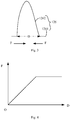
- the electrostatic force F is smaller than the predetermined threshold
- the deformation D (horizontal axis) of the deformable wire 1262 in the moving direction of the movable electrode 124 under the electrostatic force F is proportional to the electrostatic force F (vertical axis).
- the MEMS 12 has a very high moving accuracy when compared with the existing voice coil motor, and the accuracy may be in a pixel level (i.e., a distance accuracy of movement of the image sensor 14 driven by the MEMS 12 for each time may be equivalent to a pixel of the image sensor 14).
- an adjustment value between two adjacent electrostatic forces may result in a deformation D (i.e., a change in amplitude) smaller than or equal to 150 ⁇ m.
- the MEMS 12 may drive the image sensor 14 to move 150 ⁇ m, that is, a compensation capability/range of the optical image stabilization system 10 may be 150 ⁇ m (in compensation accuracy), and the MEMS 12 has a strong compensation ability when compared with the existing voice coil motor.
- the MEMS 12 may have a higher mechanical frequency due to applications of the materials, shapes and sizes of the above embodiments.
- the mechanical frequency of the MEMS 12 is typically between 80 to 120 Hz, such as 100 Hz. Therefore, due to the high mechanical frequency, the MEMS 12 may be less sensitive to sound or vibration when compared with the mechanical frequency (about 20 Hz) of the existing voice coil motor.
- a plurality of first pads 1224 are formed on an upper surface 1222 of the fixed electrode 122, and a plurality of second pads 1244 are formed on an upper surface 1242 of the movable electrode 124.
- a plurality of the deformable connection members 126 exist, and the connection tabs 1264 are fixedly connected with the first pad 1224 and the second pad 1244 respectively such that each deformable connection member 126 is configured to fixedly connect the fixed electrode 122 with the movable electrode 124.
- a plurality of the first pads 1224 may be formed on the fixed electrode 122 and a plurality of the second pads 1244 may be formed on the movable electrode 124 by the penetration and photolithography process, and the connection tabs 1264 are fixedly connected with the first pad 1224 and the second pad 1244 respectively in a wire bonding manner.
- the connection member 126 is fixedly connected with the fixed electrode 122 and the movable electrode 124 respectively.
- the fixed electrode 122 and the movable electrode 124 are fixedly connected by a plurality of connection members 126, that is, there are redundant connections. In this way, even if some of the connection members 126 are broken, the fixed electrode 122 and the movable electrode 124 may still be fixedly connected via the remaining connection members 126.
- the image sensor 14 may be fixed to the movable electrode 124 by glue.
- the optical image stabilization system 10 includes a circuit board 16, and the fixed electrode 122 is disposed on the circuit board 16.
- a plurality of third pads 164 are formed on an upper surface 162 of the circuit board 16.
- a plurality of fourth pads 1226 are formed on an upper surface 1222 of the fixed electrode 122.
- a plurality of the third pads 164 are connected to a plurality of the fourth pads 1226 via first wires 166.
- the driving voltage is applied to the fixed electrode 122 from the circuit board 16 through the first wires 166 and applied to the movable electrode 124 from the circuit board 16 through the first wires 166 and some of the connection members 126.
- connection members 126 are configured to transmit the driving voltage to the fixed electrode 122 and the movable electrode 124.
- the connection member 126 is not only functioned as a mechanical connection, but also can realize an electrical connection, thus realizing two functions at the same time, which may simplify the structure, reduce the amount of components and reduce cost.
- a plurality of fifth pads 144 are formed on an upper surface 142 of the image sensor 14, a plurality of fifth pads 144 are connected to some of the second pads 1244 via second wires 168.
- the circuit board 16 is electrically connected to the image sensor 14 via the first wires 166, some of the connection members 126, and the second wires 168.
- connection members 126 are configured to transmit control signals and image signals.
- the connection member 126 is not only functioned as a mechanical connection, but also can realize an electrical connection, thus realizing two functions at the same time, which may simplify the structure, reduce the amount of components and reduce cost.
- the circuit board 16 is a flexible circuit board.
- the optical image stabilization system 10 further includes a reinforcing plate 18 attached to a surface of the circuit board 16 opposite to the MEMS 12.
- the reinforcing plate 18 is configured to increase the mechanical strength of the circuit board 16.
- the circuit board 16 may not be limited to the embodiments described above, and may be a rigid circuit board.
- a groove 161 is defined in the circuit board 16, and the MEMS 12 and the image sensor 14 are disposed in the groove 161.
- the whole height of the optical image stabilization system 10 may be reduced, which is advantage for miniaturization.
- the fixed electrode 122 is fixed on the circuit board 16 by glue.
- an annular through recess 163 is defined in the circuit board 16 and separates the circuit board 16 into a movable part 165, and a fixed part 167 surrounding the movable part 165, in which the fixed electrode 122 is disposed on the fixed part 167 and the movable electrode 124 is disposed on the movable part 165.
- the movable electrode 124 is able to move while being fixedly connected to the circuit board 16.
- the movable electrode 124 may also be fixed to the movable part 165 by glue.
- a via hole 1246 is defined in the movable electrode 124, and the image sensor 14 is electrically connected to the movable part 165 via a conductive paste layer 169 filled in the via hole 1246.
- the fixed electrode 122 and the movable electrode 124 are pectinate electrodes cooperating with each other.
- the cooperating area between the fixed electrode 122 and the movable electrode 124 is increased, and the driving voltage is converted into the electrostatic force with a high efficiency, which may further reduce the power consumption of the optical image stabilization system 10.
- a first pair X1 of the fixed electrode 122 and the movable electrode 124, a second pair Y1 of the fixed electrode 122 and the movable electrode 124, a third pair X2 of the fixed electrode 122 and the movable electrode 124 and a fourth pair Y2 of the fixed electrode 122 and the movable electrode 124 exist, the first pair X1, the second pair Y1, the third pair X2 and the fourth pair Y2 are distributed in a shape of a Chinese character " ", the first pair X1 and the third pair X2 are configured to drive the image sensor 14 to move in a first direction (for example, an X direction) respectively, and the second pair Y1 and the fourth pair Y2 are configured to simultaneously drive the image sensor 14 to move in a second direction (for example, a Y direction) perpendicular to the first direction (for example, the X direction).
- a motion compensation may be realized in the first direction (for example, the X direction) and the second direction (for example, the Y direction), and by controlling the first pair X1 and the third pair X2 to drive the image sensor 14 to move in opposite directions, a rotation compensation may be realized in a third direction (for example, a Z direction) perpendicular to the first direction (for example, the X direction) and the second direction (for example, the Y direction).
- the MEMS 12 further includes an inner frame 11 and an outer frame 13.
- the inner frame 11 is fixedly connected to the fixed electrodes 122 of the first pair X1, the second pair Y1, the third pair X2 and the fourth pair Y2.
- the outer frame 13 is fixedly connected to the movable electrodes 124 of the first pair X1, the second pair Y1, the third pair X2 and the fourth pair Y2.
- the deformable connection member 126 is configured to fixedly connect the fixed electrode 122 with the movable electrode 124 by fixedly connecting the inner frame 11 with the outer frame 13.
- the inner frame 11 and the outer frame 13 both have a substantially rectangular shape, and an inner frame pad 112 is formed on an upper surface of the inner frame 11 and an outer frame pad 132 is formed on an upper surface of the outer frame 13.
- connection member 126 is configured to fixedly connect the inner frame 11 with the outer frame 13 by being fixedly disposed on the inner frame pad 114 and the outer frame pad 134.
Landscapes
- Engineering & Computer Science (AREA)
- Multimedia (AREA)
- Signal Processing (AREA)
- Physics & Mathematics (AREA)
- Computer Hardware Design (AREA)
- General Physics & Mathematics (AREA)
- Theoretical Computer Science (AREA)
- Human Computer Interaction (AREA)
- General Engineering & Computer Science (AREA)
- Optics & Photonics (AREA)
- Studio Devices (AREA)
- Adjustment Of Camera Lenses (AREA)
Abstract
Description
- This application claims priority to and benefits of Chinese Patent Application Serial No.
201610616350.X - The present disclosure relates to the field of an optical image stabilization technology, and more particularly to an optical image stabilization system, an imaging device and an electronic device.
- In the existing optical image stabilization system, a voice coil motor is used as an actuator and usually has a large size, which is disadvantageous for miniaturization of an imaging device and an electronic device using the existing optical image stabilization system.
- Embodiments of the present disclosure seek to solve at least one of the problems existing in the related art to at least some extent. Accordingly, embodiments of the present disclosure provide an optical image stabilization system, an imaging device and an electronic device.
- In embodiments of the present disclosure, the optical image stabilization system includes:
- a micro electro-mechanical system including:
- a fixed electrode;
- a movable electrode cooperating with the fixed electrode; and
- a deformable connection member for fixedly connecting the fixed electrode with the movable electrode; and
- an image sensor fixedly connected to the movable electrode;
- in which the fixed electrode and the movable electrode are configured to generate an electrostatic force under a driving voltage, the deformable connection member is configured to deform under the electrostatic force in a direction where the movable electrode moves, to make the movable electrode move, so as to drive the image sensor to move to compensate for a jitter.
- In embodiments of the present disclosure, a size of the micro electro-mechanical system is smaller than or equal to 88.5 mm * 8.5 mm.
- In embodiments of the present disclosure, a power consumption of the micro electro-mechanical system is smaller than 10 mW.
- In embodiments of the present disclosure, a mechanical frequency of the micro electro-mechanical system is in a range of 80 to 120 Hz.
- In embodiments of the present disclosure, the micro electro-mechanical system includes a plurality of pairs of the fixed electrodes and the movable electrodes, and the plurality of pairs of the fixed electrodes and the movable electrodes are configured to drive the image sensor to move in different directions in a same plane.
- In embodiments of the present disclosure, the deformable connection member includes a deformable wire and connection tabs connected to both ends of the deformable wire respectively.
- In embodiments of the present disclosure, the deformable wire is a silicon wire.
- In embodiments of the present disclosure, the deformable wire has a rectangular cross-section, a width of 10 to 30 µm, a thickness of 1 to 3 µm, and a length of 500 to 800 µm; a width direction of the deformable wire is perpendicular to a moving direction of the movable electrode.
- In embodiments of the present disclosure, a deformation of the deformable wire in a moving direction of the movable electrode under the electrostatic force is proportional to the electrostatic force when the electrostatic force is smaller than a predetermined threshold.
- In embodiments of the present disclosure, the deformation is smaller than or equal to 150 µm when the electrostatic force is smaller than the predetermined threshold.
- In embodiments of the present disclosure, a plurality of first pads are formed on an upper surface of the fixed electrode, and a plurality of second pads are formed on an upper surface of the movable electrode; a plurality of the deformable connection members exist, and the connection tabs are fixedly connected with the first pad and the second pad respectively such that each deformable connection member is configured to fixedly connect the fixed electrode with the movable electrode.
- In embodiments of the present disclosure, the optical image stabilization system further includes a circuit board, and the fixed electrode is disposed on the circuit board; a plurality of third pads are formed on an upper surface of the circuit board; a plurality of fourth pads are formed on an upper surface of the fixed electrode; a plurality of the third pads are connected to a plurality of the fourth pads via first wires; the driving voltage is applied to the fixed electrode from the circuit board through the first wires and applied to the movable electrode from the circuit board through the first wires and some of the connection members.
- In embodiments of the present disclosure, a plurality of fifth pads are formed on an upper surface of the image sensor, a plurality of fifth pads are connected to some of the second pads via second wires, and the circuit board is electrically connected to the image sensor via the first wires, some of the connection members and the second wires.
- In embodiments of the present disclosure, a groove is defined in the circuit board, and the micro electro-mechanical system and the image sensor are disposed in the groove.
- In embodiments of the present disclosure, an annular through recess is defined in the circuit board and separates the circuit board into a movable part and a fixed part surrounding the movable part, in which the fixed electrode is disposed on the fixed part and the movable electrode is disposed on the movable part.
- In embodiments of the present disclosure, a via hole is defined in the movable electrode, and the image sensor is electrically connected to the movable part via a conductive paste layer filled in the via hole.
- In embodiments of the present disclosure, the fixed electrode and the movable electrode are pectinate electrodes cooperating with each other.
- In embodiments of the present disclosure, the optical image stabilization system includes a first pair of the fixed electrode and the movable electrode, a second pair of the fixed electrode and the movable electrode, a third pair of the fixed electrode and the movable electrode, and a fourth pair of the fixed electrode and the movable electrode, the first pair, the second pair, the third pair, and the fourth pair are distributed in a shape of a Chinese character "", the first pair and the third pair are configured to drive the image sensor to move in a first direction respectively, and the second pair and the fourth pair are configured to simultaneously drive the image sensor to move in a second direction perpendicular to the first direction.

- In embodiments of the present disclosure, the first pair, the second pair, the third pair, and the fourth pair are further configured to drive the image sensor to rotate in a third direction perpendicular to both the first direction and the second direction by cooperating with each other.
- In embodiments of the present disclosure, the micro electro-mechanical system further includes: an inner frame fixedly connected to the fixed electrodes of the first pair, the second pair, the third pair, and the fourth pair; an outer frame fixedly connected to the movable electrodes of the first pair, the second pair, the third pair, and the fourth pair; in which the deformable connection member is configured to fixedly connect the fixed electrode with the movable electrode by fixedly connecting the inner frame with the outer frame.
- In embodiments of the present disclosure, the inner frame and the outer frame both have a rectangular shape, and an inner frame pad is formed on an upper surface of the inner frame and an outer frame pad is formed on an upper surface of the outer frame; the connection member is configured to fixedly connect the inner frame with the outer frame by being fixedly disposed on the inner frame pad and the outer frame pad.
- In embodiments of the present disclosure, the imaging device includes the optical image stabilization system described above.
- In embodiments of the present disclosure, the electronic device includes the imaging device described above.
- The micro electro-mechanical system (MEMS) is a high-tech electromechanical device developed from the microelectronics technology (the semiconductor manufacturing technology) combining photoetching, corroding, thin film forming, LIGA, silicon micromachining, non-silicon micromachining and precision machining technologies, and has a smaller size when compared with the existing voice coil motor, which is advantageous for the miniaturization of the optical image stabilization system and thus is also advantageous for the miniaturization of an imaging device using the optical image stabilization system and an electronic device using the imaging device.
- Additional aspects and advantages of embodiments of present disclosure will be given in part in the following descriptions, become apparent in part from the following descriptions, or be learned from the practice of the embodiments of the present disclosure.
- These and other aspects and advantages of embodiments of the present disclosure will become apparent and more readily appreciated from the following descriptions made with reference to the drawings, in which:
-
Fig. 1 is a schematic view of an optical image stabilization system according to an embodiment of the present disclosure. -
Fig. 2 is a schematic view of an electronic device according to an embodiment of the present disclosure. -
Fig. 3 is a schematic view of a connection member according to an embodiment of the present disclosure. -
Fig. 4 is a graph showing a force-deformation characteristic curve of a connection member according to an embodiment of the present disclosure. -
Fig. 5 is a schematic view of a micro electro-mechanical system according to another embodiment of the present disclosure. -
Fig. 6 is a schematic view of an optical image stabilization system according to another embodiment of the present disclosure. - optical
image stabilization system 10,inner frame 11,inner frame pad 112,MEMS 12,fixed electrode 122,upper surface 1222,first pad 1224,fourth pad 1226,movable electrode 124,upper surface 1242,second pad 1244, viahole 1246,connection member 126,deformable wire 1262,connection tab 1264, first pair X1, second pair Y1, third pair X2, fourth pair Y2,outer frame 13,outer frame pad 132,image sensor 14,upper surface 142,fifth pad 144,circuit board 16,groove 161,upper surface 162, annular throughrecess 163,third pad 164,movable part 165,first wire 166,fixed part 167,second wire 168,conductive paste 169, reinforcingplate 18,imaging device 20,electronic device 30. - Embodiments of the present disclosure are described in detail below, examples of which are illustrated in the drawings. The same or similar elements are denoted by same reference numerals in different drawings unless indicated otherwise. The embodiments described herein with reference to drawings are explanatory, and used to generally understand the present disclosure. The embodiments shall not be construed to limit the present disclosure.
- In the specification, it is to be understood that terms such as "central", "longitudinal", "lateral", "length", "width", "thickness", "upper", "lower", "front", "rear", "left", "right", "vertical", "horizontal", "top", "bottom", "inner", "outer", "clockwise" and "counterclockwise", should be construed to refer to the orientation as then described or as shown in the drawings under discussion. These relative terms are for convenience of description and do not require that the present invention be constructed or operated in a particular orientation, and thus shall not be construed to limit the present disclosure. In addition, it should be understood that terms such as "first" and "second" are used herein for purposes of description and are not intended to indicate or imply relative importance or significance or to imply the number of indicated technical features. Therefore, the feature defined with "first" and "second" may include one or more of this feature. In the description of the present disclosure, unless specified otherwise, "a plurality of' means two or more than two, such as two or three.
- In the present disclosure, unless specified or limited otherwise, the terms "mounted", "connected" and "coupled" and the like are used broadly, and may be, for example, fixed connections, detachable connections, or integral connections; may also be mechanical or electrical connections; may also be direct connections or indirect connections via intervening structures; may also be inner communications or inner interactions of two elements. Specific meanings of the above terms in the present disclosure can be understood by those skilled in the art according to specific conditions.
- In the present invention, unless specified or limited otherwise, a structure in which a first feature is "on" or "below" a second feature may include an embodiment in which the first feature is in direct contact with the second feature, and may also include an embodiment in which the first feature and the second feature are not in direct contact with each other, but are contacted via an additional feature formed therebetween. Furthermore, a first feature "on," "above," or "on top of' a second feature may include an embodiment in which the first feature is right or obliquely "on," "above," or "on top of' the second feature, or just means that the first feature is at a height higher than that of the second feature; while a first feature "below," "under," or "on bottom of' a second feature may include an embodiment in which the first feature is right or obliquely "below," "under," or "on bottom of' the second feature, or just means that the first feature is at a height lower than that of the second feature.
- Various embodiments and examples are provided in the following description to implement different structures of the present disclosure. In order to simplify the present disclosure, certain elements and settings will be described. However, these elements and settings are only by way of example and are not intended to limit the present disclosure. In addition, reference numerals and/or reference letters may be repeated in different examples in the present disclosure. This repeating is for the purpose of simplification and clarity and does not refer to relations between different embodiments and/or settings. Furthermore, examples of different processes and materials are provided in the present disclosure. However, it would be appreciated by those skilled in the art that other processes and/or materials may be also applied.
- As shown in
Fig. 1 , an opticalimage stabilization system 10 according to an embodiment of the present disclosure includes a micro electro-mechanical system (MEMS) 12 and animage sensor 14. TheMEMS 12 includes a fixedelectrode 122, amovable electrode 124, and adeformable connection member 126. Themovable electrode 124 cooperates with the fixedelectrode 122. Thedeformable connection member 126 is configured to fixedly connect the fixedelectrode 122 with themovable electrode 124. The fixedelectrode 122 and themovable electrode 124 are configured to generate an electrostatic force under a driving voltage. Thedeformable connection member 126 is configured to deform under the electrostatic force in a direction where themovable electrode 124 moves, to make themovable electrode 124 move, so as to drive theimage sensor 14 to move to compensate for a jitter. - The MEMS is a high-tech electromechanical device developed from the microelectronics technology (the semiconductor manufacturing technology) combining photoetching, corroding, thin film forming, LIGA, silicon micromachining, non-silicon micromachining and precision machining technologies, and has a smaller size when compared with the existing voice coil motor, which is advantageous for the miniaturization of the optical
image stabilization system 10. - For example, in some embodiments of the present disclosure, the
MEMS 12 has a size of 8.5 mm * 8.5 mm or less in a lateral dimension. Moreover, with the development of the semiconductor manufacturing technology, the size of theMEMS 12 may be smaller. - Therefore, compared with the existing voice coil motor, the
MEMS 12 has a size in a millimeter level or lower, and thus has a significant advantage in size. - With reference to
Fig. 2 , the opticalimage stabilization system 10 according to the embodiments of the present disclosure may be applied to theimaging device 20 according to the embodiments of the present disclosure, and theimaging device 20 according to the embodiments of the present disclosure may be applied to anelectronic device 30 according to the embodiments of the present disclosure. For example, theelectronic device 30 according to the embodiments of the present disclosure may be a mobile phone or a tablet computer, and theimaging device 20 according to the embodiments of the present disclosure may be a front camera or a rear camera of a mobile phone or a tablet computer. - The jitter refers to a jitter that occurs during an exposure process in using the
electronic device 30 to take pictures, which causes blurring of an image output by theimaging device 20. The imaging quality of theimaging device 20 may be improved by using the opticalimage stabilization system 10. - Moreover, by using the optical
image stabilization system 10 according to the embodiments of the present disclosure, theimaging device 20 and theelectronic device 30 according to the embodiments of the present disclosure may be advantageously miniaturized. - In addition, due to an electrostatic force actuation (i.e., an actuation based on an attraction among electrostatic charges), on one hand, the
MEMS 12 has a less power consumption when compared with the existing voice coil motor, for example, in some embodiments of the present disclosure, the power consumption of theMEMS 12 is less than 10 mW, on the other hand, theMEMS 12 has a low heat generation and thus having no problem of heat dissipation. - In some embodiments of the present disclosure, by performing thin film forming, photoetching, corroding, laser cutting, silicon micromachining, non-silicon micromachining and precision machining technologies on a silicon substrate (not shown), the fixed
electrode 122 and themovable electrode 124 may be formed, and themovable electrode 124 is floating and is connected with the fixedelectrode 122 by theconnection member 126. - In some embodiments of the present disclosure, the
MEMS 12 includes a plurality of pairs of the fixedelectrodes 122 and themovable electrodes 124, and each pair of the fixedelectrode 122 and themovable electrode 124 is configured to drive theimage sensor 14 to move in a predetermined direction in a same plane. - In this way, the plurality of pairs of the fixed
electrodes 122 and themovable electrodes 124 may compensate for jitters in different directions. Moreover, a plurality of pairs of the fixedelectrodes 122 and themovable electrodes 124 may cooperate with each other in the same plane, that is, a plurality of pairs of the fixedelectrodes 122 and themovable electrodes 124 may be in the same plane. Therefore, theMEMS 12 may have a single-layer electrode structure, which can simplify the structure of theMEMS 12, thus making theMEMS 12 simple in structure and easy to manufacture. - In some embodiments of the present disclosure, the
connection member 126 may also be formed by performing thin film forming, photoetching, corroding, laser cutting, silicon micromachining, non-silicon micromachining and precision machining technologies on a silicon substrate (not shown). - With reference to
Fig. 3 , in some embodiments of the present disclosure, theconnection member 126 includes adeformable wire 1262 and a pair ofconnection tabs 1264 connected to both ends of thedeformable wire 1262 respectively. - In this way, good mechanical connection and deformation characteristics may be provided by the
deformable wire 1262, and theconnection tab 1264 may be used to increase the connection area with the fixedelectrode 122 or themovable electrode 124, thus improving the connection strength. - In some embodiments of the present disclosure, the
deformable wire 1262 may be a silicon wire. - In this way, the
deformable wire 1262 may be manufactured by the semiconductor manufacturing technology. - In some embodiments of the present disclosure, the shape and the size of the
deformable wire 1262 may be determined according to material properties, such that themovable electrode 124 may be suspended by thedeformable wire 1262 to the fixedelectrode 122 and thedeformable wire 1262 may deform in the moving direction of themovable electrode 124. - For example, in some embodiments of the present disclosure, the
deformable wire 1262 is the silicon wire and has a rectangular cross-section, a width of 10 to 30 µm, a thickness of 1 to 3 µm, and a length of 500 to 800 µm. A width direction of thedeformable wire 1262 is perpendicular to the moving direction of themovable electrode 124 when thedeformable wire 1262 is configured to connect the fixedelectrode 122 with themovable electrode 124. - As an example, the
deformable wire 1262 has a width of 25 µm, a thickness of 1.5 µm, and a length of 600 µm. - With reference to
Fig. 4 , in settings of the shape and the size, thedeformable wire 1262 may be deformed only in the moving direction of themovable electrode 124 under an external force, and the deformation of thedeformable wire 1262 is proportional to the external force within a certain external force range (i.e., the external force is smaller than a predetermined threshold). Thedeformable wire 1262 remains rigid and is not easy to deform in other directions. On this basis, when the electrostatic force F is smaller than the predetermined threshold, the deformation D (horizontal axis) of thedeformable wire 1262 in the moving direction of themovable electrode 124 under the electrostatic force F is proportional to the electrostatic force F (vertical axis). - In this way, by precisely controlling the driving voltage, the
MEMS 12 has a very high moving accuracy when compared with the existing voice coil motor, and the accuracy may be in a pixel level (i.e., a distance accuracy of movement of theimage sensor 14 driven by theMEMS 12 for each time may be equivalent to a pixel of the image sensor 14). - In some embodiments of the present disclosure, when the electrostatic force F is smaller than a predetermined threshold, an adjustment value between two adjacent electrostatic forces may result in a deformation D (i.e., a change in amplitude) smaller than or equal to 150 µm.
- In other words, the
MEMS 12 may drive theimage sensor 14 to move 150 µm, that is, a compensation capability/range of the opticalimage stabilization system 10 may be 150 µm (in compensation accuracy), and theMEMS 12 has a strong compensation ability when compared with the existing voice coil motor. - In addition, the
MEMS 12 may have a higher mechanical frequency due to applications of the materials, shapes and sizes of the above embodiments. For example, in some embodiments of the present disclosure, the mechanical frequency of theMEMS 12 is typically between 80 to 120 Hz, such as 100 Hz. Therefore, due to the high mechanical frequency, theMEMS 12 may be less sensitive to sound or vibration when compared with the mechanical frequency (about 20 Hz) of the existing voice coil motor. - In some embodiments of the present disclosure, a plurality of
first pads 1224 are formed on anupper surface 1222 of the fixedelectrode 122, and a plurality ofsecond pads 1244 are formed on anupper surface 1242 of themovable electrode 124. A plurality of thedeformable connection members 126 exist, and theconnection tabs 1264 are fixedly connected with thefirst pad 1224 and thesecond pad 1244 respectively such that eachdeformable connection member 126 is configured to fixedly connect the fixedelectrode 122 with themovable electrode 124. - In some embodiments of the present disclosure, a plurality of the
first pads 1224 may be formed on the fixedelectrode 122 and a plurality of thesecond pads 1244 may be formed on themovable electrode 124 by the penetration and photolithography process, and theconnection tabs 1264 are fixedly connected with thefirst pad 1224 and thesecond pad 1244 respectively in a wire bonding manner. In this way, it may be ensured that theconnection member 126 is fixedly connected with the fixedelectrode 122 and themovable electrode 124 respectively. Moreover, since the fixedelectrode 122 and themovable electrode 124 are fixedly connected by a plurality ofconnection members 126, that is, there are redundant connections. In this way, even if some of theconnection members 126 are broken, the fixedelectrode 122 and themovable electrode 124 may still be fixedly connected via the remainingconnection members 126. - In some embodiments of the present disclosure, the
image sensor 14 may be fixed to themovable electrode 124 by glue. - In this way, the process is simple, thus facilitating the manufacture.
- In some embodiments of the present disclosure, the optical
image stabilization system 10 includes acircuit board 16, and the fixedelectrode 122 is disposed on thecircuit board 16. A plurality ofthird pads 164 are formed on anupper surface 162 of thecircuit board 16. A plurality offourth pads 1226 are formed on anupper surface 1222 of the fixedelectrode 122. A plurality of thethird pads 164 are connected to a plurality of thefourth pads 1226 viafirst wires 166. The driving voltage is applied to the fixedelectrode 122 from thecircuit board 16 through thefirst wires 166 and applied to themovable electrode 124 from thecircuit board 16 through thefirst wires 166 and some of theconnection members 126. - In this way, some of the
connection members 126 are configured to transmit the driving voltage to the fixedelectrode 122 and themovable electrode 124. Theconnection member 126 is not only functioned as a mechanical connection, but also can realize an electrical connection, thus realizing two functions at the same time, which may simplify the structure, reduce the amount of components and reduce cost. - A plurality of
fifth pads 144 are formed on anupper surface 142 of theimage sensor 14, a plurality offifth pads 144 are connected to some of thesecond pads 1244 viasecond wires 168. Thecircuit board 16 is electrically connected to theimage sensor 14 via thefirst wires 166, some of theconnection members 126, and thesecond wires 168. - In this way, some of the
connection members 126 are configured to transmit control signals and image signals. Theconnection member 126 is not only functioned as a mechanical connection, but also can realize an electrical connection, thus realizing two functions at the same time, which may simplify the structure, reduce the amount of components and reduce cost. - In some embodiments of the present disclosure, the
circuit board 16 is a flexible circuit board. The opticalimage stabilization system 10 further includes a reinforcingplate 18 attached to a surface of thecircuit board 16 opposite to theMEMS 12. The reinforcingplate 18 is configured to increase the mechanical strength of thecircuit board 16. - Alternatively, in other embodiments of the present disclosure, the
circuit board 16 may not be limited to the embodiments described above, and may be a rigid circuit board. - In some embodiments of the present disclosure, a
groove 161 is defined in thecircuit board 16, and theMEMS 12 and theimage sensor 14 are disposed in thegroove 161. - In this way, the whole height of the optical
image stabilization system 10 may be reduced, which is advantage for miniaturization. - In some embodiments of the present disclosure, the fixed
electrode 122 is fixed on thecircuit board 16 by glue. - In this way, the process is simple, thus facilitating the manufacture.
- In some embodiments of the present disclosure, an annular through
recess 163 is defined in thecircuit board 16 and separates thecircuit board 16 into amovable part 165, and afixed part 167 surrounding themovable part 165, in which the fixedelectrode 122 is disposed on thefixed part 167 and themovable electrode 124 is disposed on themovable part 165. - In this way, the
movable electrode 124 is able to move while being fixedly connected to thecircuit board 16. - The
movable electrode 124 may also be fixed to themovable part 165 by glue. - In some embodiments of the present disclosure, a via
hole 1246 is defined in themovable electrode 124, and theimage sensor 14 is electrically connected to themovable part 165 via aconductive paste layer 169 filled in the viahole 1246. - With reference to
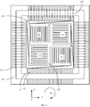
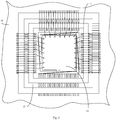
Figs. 5 and6 , in some embodiments of the present disclosure, the fixedelectrode 122 and themovable electrode 124 are pectinate electrodes cooperating with each other. - When the pectinate electrode is applied, the cooperating area between the fixed
electrode 122 and themovable electrode 124 is increased, and the driving voltage is converted into the electrostatic force with a high efficiency, which may further reduce the power consumption of the opticalimage stabilization system 10. - A first pair X1 of the fixed
electrode 122 and themovable electrode 124, a second pair Y1 of the fixedelectrode 122 and themovable electrode 124, a third pair X2 of the fixedelectrode 122 and themovable electrode 124 and a fourth pair Y2 of the fixedelectrode 122 and themovable electrode 124 exist, the first pair X1, the second pair Y1, the third pair X2 and the fourth pair Y2 are distributed in a shape of a Chinese character "", the first pair X1 and the third pair X2 are configured to drive theimage sensor 14 to move in a first direction (for example, an X direction) respectively, and the second pair Y1 and the fourth pair Y2 are configured to simultaneously drive theimage sensor 14 to move in a second direction (for example, a Y direction) perpendicular to the first direction (for example, the X direction). - In this way, a motion compensation may be realized in the first direction (for example, the X direction) and the second direction (for example, the Y direction), and by controlling the first pair X1 and the third pair X2 to drive the
image sensor 14 to move in opposite directions, a rotation compensation may be realized in a third direction (for example, a Z direction) perpendicular to the first direction (for example, the X direction) and the second direction (for example, the Y direction). - In some embodiments of the present disclosure, the
MEMS 12 further includes aninner frame 11 and anouter frame 13. Theinner frame 11 is fixedly connected to the fixedelectrodes 122 of the first pair X1, the second pair Y1, the third pair X2 and the fourth pair Y2. Theouter frame 13 is fixedly connected to themovable electrodes 124 of the first pair X1, the second pair Y1, the third pair X2 and the fourth pair Y2. Thedeformable connection member 126 is configured to fixedly connect the fixedelectrode 122 with themovable electrode 124 by fixedly connecting theinner frame 11 with theouter frame 13. - In this way, the process is simple, thus facilitating the manufacture.
- In some embodiments of the present disclosure, the
inner frame 11 and theouter frame 13 both have a substantially rectangular shape, and aninner frame pad 112 is formed on an upper surface of theinner frame 11 and anouter frame pad 132 is formed on an upper surface of theouter frame 13. - The
connection member 126 is configured to fixedly connect theinner frame 11 with theouter frame 13 by being fixedly disposed on the inner frame pad 114 and the outer frame pad 134. - In this way, the process is simple, thus facilitating for manufacture.
- Reference throughout this specification to "an embodiment", "some embodiments", "an example", "a specific example", or "some examples" means that a particular feature, structure, material, or characteristic described in connection with the embodiment or example is included in at least one embodiment or example of the present disclosure. The appearances of above phrases in various places throughout this specification are not necessarily referring to the same embodiment or example of the present disclosure. Furthermore, the particular features, structures, materials, or characteristics may be combined in any suitable manner in one or more embodiments or examples.
- Although explanatory embodiments have been shown and described above, it would be appreciated by those skilled in the art that the above embodiments cannot be construed to limit the present disclosure, and changes, alternatives, and modifications can be made in the embodiments without departing from spirit, principles and scope of the present disclosure.
Claims (23)
- An optical image stabilization system, comprising:a micro electro-mechanical system comprising:a fixed electrode;a movable electrode cooperating with the fixed electrode; anda deformable connection member for fixedly connecting the fixed electrode with the movable electrode; andan image sensor fixedly connected to the movable electrode;wherein the fixed electrode and the movable electrode are configured to generate an electrostatic force under a driving voltage, the deformable connection member is configured to deform under the electrostatic force in a direction where the movable electrode moves, to make the movable electrode move, so as to drive the image sensor to move to compensate for a jitter.
- The optical image stabilization system according to claim 1, wherein a size of the micro electro-mechanical system is smaller than or equal to 88.5 mm * 8.5 mm.
- The optical image stabilization system according to claim 1, wherein a power consumption of the micro electro-mechanical system is smaller than 10 mW.
- The optical image stabilization system according to claim 1, wherein a mechanical frequency of the micro electro-mechanical system is in a range of 80 to 120 Hz.
- The optical image stabilization system according to claim 1, wherein the micro electro-mechanical system comprises a plurality of pairs of the fixed electrodes and the movable electrodes, and the plurality of pairs of the fixed electrodes and the movable electrodes are configured to drive the image sensor to move in different directions in a same plane.
- The optical image stabilization system according to claim 1, wherein the deformable connection member comprises a deformable wire and connection tabs connected to both ends of the deformable wire respectively.
- The optical image stabilization system according to claim 6, wherein the deformable wire is a silicon wire.
- The optical image stabilization system according to claim 7, wherein the deformable wire has a rectangular cross-section, a width of 10 to 30 µm, a thickness of 1 to 3 µm, and a length of 500 to 800 µm;
a width direction of the deformable wire is perpendicular to a moving direction of the movable electrode. - The optical image stabilization system according to claim 7, wherein a deformation of the deformable wire in a moving direction of the movable electrode under the electrostatic force is proportional to the electrostatic force when the electrostatic force is smaller than a predetermined threshold.
- The optical image stabilization system according to claim 9, wherein the deformation is smaller than or equal to 150 µm when the electrostatic force is smaller than the predetermined threshold.
- The optical image stabilization system according to claim 6, wherein a plurality of first pads formed on an upper surface of the fixed electrode, and a plurality of second pads are formed on an upper surface of the movable electrode;
a plurality of the deformable connection members exist, and the connection tabs are fixedly connected with the first pad and the second pad respectively such that each deformable connection member is configured to fixedly connect the fixed electrode with the movable electrode. - The optical image stabilization system according to claim 6, wherein the optical image stabilization system further comprises a circuit board, and the fixed electrode is disposed on the circuit board;
a plurality of third pads are formed on an upper surface of the circuit board;
a plurality of fourth pads are formed on an upper surface of the fixed electrode;
the plurality of the third pads are connected to the plurality of the fourth pads via first wires;
the driving voltage is applied to the fixed electrode from the circuit board through the first wires and applied to the movable electrode from the circuit board through the first wires and some of the connection members. - The optical image stabilization system according to claim 12, wherein a plurality of fifth pads are formed on an upper surface of the image sensor, the plurality of fifth pads are connected to some of the second pads via second wires, and the circuit board is electrically connected to the image sensor via the first wires, some of the connection members and the second wires.
- The optical image stabilization system according to claim 12, wherein a groove is defined in the circuit board, and the micro electro-mechanical system and the image sensor are disposed in the groove.
- The optical image stabilization system according to claim 14, wherein an annular through recess is defined in the circuit board and separates the circuit board into a movable part and a fixed part surrounding the movable part, in which the fixed electrode is disposed on the fixed part and the movable electrode is disposed on the movable part.
- The optical image stabilization system according to claim 15, wherein a via hole is defined in the movable electrode, and the image sensor is electrically connected to the movable part via a conductive paste layer filled in the via hole.
- The optical image stabilization system according to claim 1, wherein the fixed electrode and the movable electrode are pectinate electrodes cooperating with each other.
- The optical image stabilization system according to claim 17, wherein the optical image stabilization system comprises a first pair of the fixed electrode and the movable electrode, a second pair of the fixed electrode and the movable electrode, a third pair of the fixed electrode and the movable electrode, and a fourth pair of the fixed electrode and the movable electrode, the first pair, the second pair, the third pair, and the fourth pair are distributed in a shape of a Chinese character "", the first pair and the third pair are configured to drive the image sensor to move in a first direction respectively, and the second pair and the fourth pair are configured to simultaneously drive the image sensor to move in a second direction perpendicular to the first direction.

- The optical image stabilization system according to claim 18, wherein the first pair, the second pair, the third pair, and the fourth pair are further configured to drive the image sensor to rotate in a third direction perpendicular to both the first direction and the second direction by cooperating with each other.
- The optical image stabilization system according to claim 18, wherein the micro electro-mechanical system further comprises:an inner frame fixedly connected to the fixed electrodes of the first pair, the second pair, the third pair, and the fourth pair;an outer frame fixedly connected to the movable electrodes of the first pair, the second pair, the third pair, and the fourth pair;wherein the deformable connection member is configured to fixedly connect the fixed electrode with the movable electrode by fixedly connecting the inner frame with the outer frame.
- The optical image stabilization system according to claim 20, wherein the inner frame and the outer frame both have a rectangular shape, and an inner frame pad is formed on an upper surface of the inner frame and an outer frame pad is formed on an upper surface of the outer frame;
the connection member is configured to fixedly connect the inner frame with the outer frame by being fixedly disposed on the inner frame pad and the outer frame pad. - An imaging device, comprising an optical image stabilization system according to any one of claims 1 to 21.
- An electronic device, comprising an imaging device according to claim 22.
Applications Claiming Priority (2)
| Application Number | Priority Date | Filing Date | Title |
|---|---|---|---|
| CN201610616350.XA CN106254773B (en) | 2016-07-29 | 2016-07-29 | Optical image stabilization system, imaging device and electronic device |
| PCT/CN2017/084217 WO2018018998A1 (en) | 2016-07-29 | 2017-05-12 | Imaging method, imaging device, and electronic device |
Publications (3)
| Publication Number | Publication Date |
|---|---|
| EP3454543A1 true EP3454543A1 (en) | 2019-03-13 |
| EP3454543A4 EP3454543A4 (en) | 2019-04-24 |
| EP3454543B1 EP3454543B1 (en) | 2022-12-28 |
Family
ID=57605994
Family Applications (1)
| Application Number | Title | Priority Date | Filing Date |
|---|---|---|---|
| EP17833303.5A Active EP3454543B1 (en) | 2016-07-29 | 2017-05-12 | Imaging method, imaging device, and electronic device |
Country Status (4)
| Country | Link |
|---|---|
| US (2) | US10721402B2 (en) |
| EP (1) | EP3454543B1 (en) |
| CN (2) | CN107948532B (en) |
| WO (1) | WO2018018998A1 (en) |
Families Citing this family (21)
| Publication number | Priority date | Publication date | Assignee | Title |
|---|---|---|---|---|
| CN107948532B (en) | 2016-07-29 | 2019-08-20 | Oppo广东移动通信有限公司 | Optical image stabilization system, imaging device and electronic device |
| CN108702435B (en) * | 2017-04-26 | 2020-07-28 | 华为技术有限公司 | Terminal and camera |
| US20200036872A1 (en) * | 2018-07-24 | 2020-01-30 | Gopro, Inc. | Module isolation |
| CN110858868B (en) * | 2018-08-23 | 2022-01-14 | 江西晶浩光学有限公司 | Camera module and photosensitive assembly thereof |
| WO2020103688A1 (en) * | 2018-11-23 | 2020-05-28 | 华为技术有限公司 | Imaging apparatus and terminal device |
| CN111225130B (en) | 2018-11-23 | 2021-02-26 | 华为机器有限公司 | Imaging device and terminal equipment |
| CN112188047B (en) * | 2019-07-05 | 2021-08-03 | 华为技术有限公司 | Image Sensor Assembly and Camera Assembly |
| CN112995450A (en) * | 2019-12-16 | 2021-06-18 | 中芯集成电路(宁波)有限公司 | Imaging module and manufacturing method thereof |
| CN113055556B (en) * | 2019-12-27 | 2022-07-08 | 中芯集成电路(宁波)有限公司 | Moving mechanism and driving method thereof, electronic equipment and imaging module |
| CN113067977B (en) * | 2019-12-31 | 2023-04-18 | 中芯集成电路(宁波)有限公司 | Translation mechanism, forming method thereof, translation method and electronic equipment |
| CN113132611B (en) * | 2019-12-31 | 2022-08-12 | 中芯集成电路(宁波)有限公司 | Mobile unit, driving method thereof, electronic equipment and camera module |
| CN113965691B (en) * | 2020-07-21 | 2022-12-02 | 中芯集成电路(宁波)有限公司上海分公司 | Moving mechanism, forming method thereof, driving method thereof, electronic device and imaging device |
| CN113992814A (en) | 2020-07-27 | 2022-01-28 | 华为技术有限公司 | Voice coil motor, camera module and electronic equipment |
| CN114765651A (en) * | 2021-01-11 | 2022-07-19 | 南昌欧菲光电技术有限公司 | Circuit board assembly, camera module and electronic equipment |
| WO2022147839A1 (en) * | 2021-01-11 | 2022-07-14 | 欧菲光集团股份有限公司 | Circuit board assembly, camera module, and electronic device |
| TWI759114B (en) * | 2021-01-20 | 2022-03-21 | 大陽科技股份有限公司 | Optical image stabilizer, camera module and electronic device |
| CN112911116B (en) * | 2021-01-29 | 2022-10-25 | 联想(北京)有限公司 | Electronic equipment |
| CN118540586A (en) * | 2021-05-20 | 2024-08-23 | 华为技术有限公司 | Camera module and electronic device using image sensor displacement anti-shake |
| KR102632373B1 (en) * | 2021-12-28 | 2024-02-02 | 삼성전기주식회사 | Sensor shifting actuator and camera module including the same |
| US12219256B1 (en) * | 2022-09-22 | 2025-02-04 | Apple Inc. | Variable flexure arm sizes for flexure module of camera with moveable image sensor |
| DE102023211945A1 (en) * | 2023-11-29 | 2025-06-05 | Robert Bosch Gesellschaft mit beschränkter Haftung | Microelectromechanical holding device, image sensor device and method for producing a microelectromechanical holding device |
Family Cites Families (36)
| Publication number | Priority date | Publication date | Assignee | Title |
|---|---|---|---|---|
| CN100339738C (en) * | 2004-03-12 | 2007-09-26 | 先进微系统科技股份有限公司 | Microelectromechanical actuator with multiple sets of comb electrodes and manufacturing method thereof |
| KR100584424B1 (en) * | 2004-11-04 | 2006-05-26 | 삼성전자주식회사 | Image stabilizer in camera lens assembly |
| US7214919B2 (en) * | 2005-02-08 | 2007-05-08 | Micron Technology, Inc. | Microelectronic imaging units and methods of manufacturing microelectronic imaging units |
| JP4700555B2 (en) | 2006-05-02 | 2011-06-15 | 三星電子株式会社 | Image blur correction device |
| JP5098254B2 (en) | 2006-08-29 | 2012-12-12 | 富士通株式会社 | Micro oscillating device |
| CN101420526B (en) * | 2007-10-26 | 2011-06-08 | 鸿富锦精密工业(深圳)有限公司 | Image sensor bearing device and camera module group |
| CN101668382B (en) * | 2009-09-30 | 2012-04-18 | 华为终端有限公司 | Flexible printed circuit board and terminal |
| WO2012005062A1 (en) | 2010-07-06 | 2012-01-12 | 日立オートモーティブシステムズ株式会社 | Inertia sensor |
| KR101075710B1 (en) * | 2010-07-15 | 2011-10-21 | 삼성전기주식회사 | Optical image stabilization device and manufacturing method thereof |
| US8513746B2 (en) | 2010-10-15 | 2013-08-20 | Rohm Co., Ltd. | MEMS sensor and method for producing MEMS sensor, and MEMS package |
| EP2439172B1 (en) * | 2010-10-06 | 2018-05-02 | Sercel | Anti-stiction method in an inertial MEMS |
| JP5822177B2 (en) | 2011-05-20 | 2015-11-24 | セイコーエプソン株式会社 | Gyro sensor, electronic equipment |
| CN103297665A (en) * | 2012-02-22 | 2013-09-11 | 庄佑华 | Image acquisition system |
| CN102624397B (en) * | 2012-03-22 | 2014-12-17 | 哈尔滨工程大学 | High-linearity fully differential digital micro-accelerometer interface circuit system |
| JP6020793B2 (en) * | 2012-04-02 | 2016-11-02 | セイコーエプソン株式会社 | Physical quantity sensor and electronic equipment |
| JP6263740B2 (en) * | 2013-10-08 | 2018-01-24 | パナソニックIpマネジメント株式会社 | Imaging device |
| JP6299142B2 (en) | 2013-10-21 | 2018-03-28 | セイコーエプソン株式会社 | Vibrator, vibrator manufacturing method, electronic device, electronic apparatus, and moving body |
| US9162868B2 (en) * | 2013-11-27 | 2015-10-20 | Infineon Technologies Ag | MEMS device |
| CN103762187B (en) * | 2014-01-16 | 2017-11-03 | 苏州晶方半导体科技股份有限公司 | chip packaging method and structure |
| JP6331535B2 (en) | 2014-03-18 | 2018-05-30 | セイコーエプソン株式会社 | Electronic devices, electronic devices, and moving objects |
| JP2015184009A (en) | 2014-03-20 | 2015-10-22 | セイコーエプソン株式会社 | Vibration element, electronic device, and moving object |
| JP6299322B2 (en) | 2014-03-25 | 2018-03-28 | セイコーエプソン株式会社 | Physical quantity detection sensor, electronic device, mobile object and electronic circuit |
| WO2015153017A2 (en) * | 2014-04-04 | 2015-10-08 | Mems Start, Llc | Actuator for moving an optoelectronic device |
| EP3140563A4 (en) | 2014-05-06 | 2018-01-17 | Mems Drive Inc. | Low stiffness flexure |
| US9578217B2 (en) * | 2014-05-27 | 2017-02-21 | Mems Drive, Inc. | Moving image sensor package |
| JP2016090254A (en) | 2014-10-30 | 2016-05-23 | セイコーエプソン株式会社 | Vibration element, electronic device, electronic device, and moving object |
| TW201630407A (en) * | 2015-02-13 | 2016-08-16 | Ue Technology Co Ltd | Image sensor system chip having image stabilization function and manufacturing method thereof |
| CN104717434B (en) * | 2015-03-27 | 2017-09-08 | 有医科技股份有限公司 | CIS System on Chip/SoC and its preparation method with image stabilization function |
| CN105025657B (en) * | 2015-08-07 | 2018-08-14 | 深圳市世尊科技有限公司 | A kind of flexible PCB for welding image sensor |
| JP6641899B2 (en) | 2015-11-04 | 2020-02-05 | セイコーエプソン株式会社 | Physical quantity sensor, physical quantity sensor device, electronic equipment and moving object |
| KR102487393B1 (en) | 2016-04-15 | 2023-01-12 | 에스케이하이닉스 주식회사 | Image Sensor Having a Light Field Mode and a Conventional Mode |
| CN105789233B (en) * | 2016-04-15 | 2019-12-17 | 格科微电子(上海)有限公司 | Photosensitive element mobile optical anti-shake method of CMOS image sensor module |
| CN107948532B (en) * | 2016-07-29 | 2019-08-20 | Oppo广东移动通信有限公司 | Optical image stabilization system, imaging device and electronic device |
| CN106161979B (en) * | 2016-07-29 | 2017-08-25 | 广东欧珀移动通信有限公司 | High dynamic range image shooting method, device and terminal equipment |
| JP6782649B2 (en) | 2017-02-28 | 2020-11-11 | 株式会社日立製作所 | Ultrasound imaging device |
| US10582100B1 (en) * | 2019-01-04 | 2020-03-03 | Faez Ba-Tis | Five degrees of freedom MEMS actuator for autofocus, optical image stabilization, and super resolution imaging in miniature cameras |
-
2016
- 2016-07-29 CN CN201711476798.7A patent/CN107948532B/en active Active
- 2016-07-29 CN CN201610616350.XA patent/CN106254773B/en active Active
-
2017
- 2017-05-12 EP EP17833303.5A patent/EP3454543B1/en active Active
- 2017-05-12 WO PCT/CN2017/084217 patent/WO2018018998A1/en not_active Ceased
-
2018
- 2018-11-20 US US16/196,704 patent/US10721402B2/en active Active
-
2019
- 2019-06-10 US US16/436,175 patent/US10582128B2/en active Active
Also Published As
| Publication number | Publication date |
|---|---|
| CN107948532A (en) | 2018-04-20 |
| US10721402B2 (en) | 2020-07-21 |
| CN106254773B (en) | 2018-01-23 |
| US20190297261A1 (en) | 2019-09-26 |
| US20190089902A1 (en) | 2019-03-21 |
| CN107948532B (en) | 2019-08-20 |
| US10582128B2 (en) | 2020-03-03 |
| EP3454543A4 (en) | 2019-04-24 |
| EP3454543B1 (en) | 2022-12-28 |
| WO2018018998A1 (en) | 2018-02-01 |
| CN106254773A (en) | 2016-12-21 |
Similar Documents
| Publication | Publication Date | Title |
|---|---|---|
| EP3454543A1 (en) | Imaging method, imaging device, and electronic device | |
| US9502464B2 (en) | Method of manufacturing optical image stabilizer | |
| US10389943B2 (en) | Actuator for moving an optoelectronic device | |
| US7489340B2 (en) | Optical image stabilizer for camera lens assembly | |
| US7692362B2 (en) | Actuating device, fabricating method thereof, and module variation control device using the actuating device | |
| EP3126285A2 (en) | Actuator for moving an optoelectronic device | |
| US12493180B2 (en) | Microelectromechanical mirror device with piezoelectric actuation having improved stress resistance | |
| US20250055388A1 (en) | Transducer wiring board and method for manufacturing the same | |
| KR101015679B1 (en) | Drive Actuator with Carbon Nanotubes | |
| CN115426448A (en) | Photosensitive assembly, camera module and preparation method of photosensitive assembly | |
| CN113132570A (en) | Imaging module and electronic equipment | |
| JP5277977B2 (en) | Optical device | |
| CN113067977B (en) | Translation mechanism, forming method thereof, translation method and electronic equipment | |
| KR20140116737A (en) | Camera Module | |
| WO2022206402A1 (en) | Actuator, actuator assembly, electronic module, and electronic device | |
| JP5120243B2 (en) | Optical device | |
| JP5527152B2 (en) | Optical deflection device | |
| CN114979428A (en) | Camera shooting assembly and electronic equipment | |
| WO2021120573A1 (en) | Imaging module and method for manufacturing same | |
| JP2016146426A (en) | Piezoelectric body, vibrator, vibration wave motor, and method of forming electrodes of piezoelectric body |
Legal Events
| Date | Code | Title | Description |
|---|---|---|---|
| STAA | Information on the status of an ep patent application or granted ep patent |
Free format text: STATUS: THE INTERNATIONAL PUBLICATION HAS BEEN MADE |
|
| PUAI | Public reference made under article 153(3) epc to a published international application that has entered the european phase |
Free format text: ORIGINAL CODE: 0009012 |
|
| STAA | Information on the status of an ep patent application or granted ep patent |
Free format text: STATUS: REQUEST FOR EXAMINATION WAS MADE |
|
| 17P | Request for examination filed |
Effective date: 20181204 |
|
| AK | Designated contracting states |
Kind code of ref document: A1 Designated state(s): AL AT BE BG CH CY CZ DE DK EE ES FI FR GB GR HR HU IE IS IT LI LT LU LV MC MK MT NL NO PL PT RO RS SE SI SK SM TR |
|
| AX | Request for extension of the european patent |
Extension state: BA ME |
|
| REG | Reference to a national code |
Ref country code: DE Ref legal event code: R079 Ref document number: 602017065075 Country of ref document: DE Free format text: PREVIOUS MAIN CLASS: H04N0005232000 Ipc: H04N0005225000 |
|
| A4 | Supplementary search report drawn up and despatched |
Effective date: 20190321 |
|
| RIC1 | Information provided on ipc code assigned before grant |
Ipc: H04N 5/225 20060101AFI20190315BHEP Ipc: H04N 5/232 20060101ALI20190315BHEP |
|
| DAV | Request for validation of the european patent (deleted) | ||
| DAX | Request for extension of the european patent (deleted) | ||
| RAP1 | Party data changed (applicant data changed or rights of an application transferred) |
Owner name: GUANGDONG OPPO MOBILE TELECOMMUNICATIONS CORP., LT |
|
| STAA | Information on the status of an ep patent application or granted ep patent |
Free format text: STATUS: EXAMINATION IS IN PROGRESS |
|
| 17Q | First examination report despatched |
Effective date: 20210217 |
|
| GRAP | Despatch of communication of intention to grant a patent |
Free format text: ORIGINAL CODE: EPIDOSNIGR1 |
|
| STAA | Information on the status of an ep patent application or granted ep patent |
Free format text: STATUS: GRANT OF PATENT IS INTENDED |
|
| INTG | Intention to grant announced |
Effective date: 20220802 |
|
| GRAS | Grant fee paid |
Free format text: ORIGINAL CODE: EPIDOSNIGR3 |
|
| GRAA | (expected) grant |
Free format text: ORIGINAL CODE: 0009210 |
|
| STAA | Information on the status of an ep patent application or granted ep patent |
Free format text: STATUS: THE PATENT HAS BEEN GRANTED |
|
| AK | Designated contracting states |
Kind code of ref document: B1 Designated state(s): AL AT BE BG CH CY CZ DE DK EE ES FI FR GB GR HR HU IE IS IT LI LT LU LV MC MK MT NL NO PL PT RO RS SE SI SK SM TR |
|
| REG | Reference to a national code |
Ref country code: GB Ref legal event code: FG4D |
|
| REG | Reference to a national code |
Ref country code: CH Ref legal event code: EP |
|
| REG | Reference to a national code |
Ref country code: DE Ref legal event code: R096 Ref document number: 602017065075 Country of ref document: DE |
|
| REG | Reference to a national code |
Ref country code: AT Ref legal event code: REF Ref document number: 1541186 Country of ref document: AT Kind code of ref document: T Effective date: 20230115 |
|
| REG | Reference to a national code |
Ref country code: IE Ref legal event code: FG4D |
|
| REG | Reference to a national code |
Ref country code: LT Ref legal event code: MG9D |
|
| PG25 | Lapsed in a contracting state [announced via postgrant information from national office to epo] |
Ref country code: SE Free format text: LAPSE BECAUSE OF FAILURE TO SUBMIT A TRANSLATION OF THE DESCRIPTION OR TO PAY THE FEE WITHIN THE PRESCRIBED TIME-LIMIT Effective date: 20221228 Ref country code: NO Free format text: LAPSE BECAUSE OF FAILURE TO SUBMIT A TRANSLATION OF THE DESCRIPTION OR TO PAY THE FEE WITHIN THE PRESCRIBED TIME-LIMIT Effective date: 20230328 Ref country code: LT Free format text: LAPSE BECAUSE OF FAILURE TO SUBMIT A TRANSLATION OF THE DESCRIPTION OR TO PAY THE FEE WITHIN THE PRESCRIBED TIME-LIMIT Effective date: 20221228 Ref country code: FI Free format text: LAPSE BECAUSE OF FAILURE TO SUBMIT A TRANSLATION OF THE DESCRIPTION OR TO PAY THE FEE WITHIN THE PRESCRIBED TIME-LIMIT Effective date: 20221228 |
|
| REG | Reference to a national code |
Ref country code: NL Ref legal event code: MP Effective date: 20221228 |
|
| REG | Reference to a national code |
Ref country code: AT Ref legal event code: MK05 Ref document number: 1541186 Country of ref document: AT Kind code of ref document: T Effective date: 20221228 |
|
| PG25 | Lapsed in a contracting state [announced via postgrant information from national office to epo] |
Ref country code: RS Free format text: LAPSE BECAUSE OF FAILURE TO SUBMIT A TRANSLATION OF THE DESCRIPTION OR TO PAY THE FEE WITHIN THE PRESCRIBED TIME-LIMIT Effective date: 20221228 Ref country code: LV Free format text: LAPSE BECAUSE OF FAILURE TO SUBMIT A TRANSLATION OF THE DESCRIPTION OR TO PAY THE FEE WITHIN THE PRESCRIBED TIME-LIMIT Effective date: 20221228 Ref country code: HR Free format text: LAPSE BECAUSE OF FAILURE TO SUBMIT A TRANSLATION OF THE DESCRIPTION OR TO PAY THE FEE WITHIN THE PRESCRIBED TIME-LIMIT Effective date: 20221228 Ref country code: GR Free format text: LAPSE BECAUSE OF FAILURE TO SUBMIT A TRANSLATION OF THE DESCRIPTION OR TO PAY THE FEE WITHIN THE PRESCRIBED TIME-LIMIT Effective date: 20230329 |
|
| P01 | Opt-out of the competence of the unified patent court (upc) registered |
Effective date: 20230412 |
|
| PG25 | Lapsed in a contracting state [announced via postgrant information from national office to epo] |
Ref country code: NL Free format text: LAPSE BECAUSE OF FAILURE TO SUBMIT A TRANSLATION OF THE DESCRIPTION OR TO PAY THE FEE WITHIN THE PRESCRIBED TIME-LIMIT Effective date: 20221228 |
|
| PG25 | Lapsed in a contracting state [announced via postgrant information from national office to epo] |
Ref country code: SM Free format text: LAPSE BECAUSE OF FAILURE TO SUBMIT A TRANSLATION OF THE DESCRIPTION OR TO PAY THE FEE WITHIN THE PRESCRIBED TIME-LIMIT Effective date: 20221228 Ref country code: RO Free format text: LAPSE BECAUSE OF FAILURE TO SUBMIT A TRANSLATION OF THE DESCRIPTION OR TO PAY THE FEE WITHIN THE PRESCRIBED TIME-LIMIT Effective date: 20221228 Ref country code: PT Free format text: LAPSE BECAUSE OF FAILURE TO SUBMIT A TRANSLATION OF THE DESCRIPTION OR TO PAY THE FEE WITHIN THE PRESCRIBED TIME-LIMIT Effective date: 20230428 Ref country code: ES Free format text: LAPSE BECAUSE OF FAILURE TO SUBMIT A TRANSLATION OF THE DESCRIPTION OR TO PAY THE FEE WITHIN THE PRESCRIBED TIME-LIMIT Effective date: 20221228 Ref country code: EE Free format text: LAPSE BECAUSE OF FAILURE TO SUBMIT A TRANSLATION OF THE DESCRIPTION OR TO PAY THE FEE WITHIN THE PRESCRIBED TIME-LIMIT Effective date: 20221228 Ref country code: CZ Free format text: LAPSE BECAUSE OF FAILURE TO SUBMIT A TRANSLATION OF THE DESCRIPTION OR TO PAY THE FEE WITHIN THE PRESCRIBED TIME-LIMIT Effective date: 20221228 Ref country code: AT Free format text: LAPSE BECAUSE OF FAILURE TO SUBMIT A TRANSLATION OF THE DESCRIPTION OR TO PAY THE FEE WITHIN THE PRESCRIBED TIME-LIMIT Effective date: 20221228 |
|
| PG25 | Lapsed in a contracting state [announced via postgrant information from national office to epo] |
Ref country code: SK Free format text: LAPSE BECAUSE OF FAILURE TO SUBMIT A TRANSLATION OF THE DESCRIPTION OR TO PAY THE FEE WITHIN THE PRESCRIBED TIME-LIMIT Effective date: 20221228 Ref country code: PL Free format text: LAPSE BECAUSE OF FAILURE TO SUBMIT A TRANSLATION OF THE DESCRIPTION OR TO PAY THE FEE WITHIN THE PRESCRIBED TIME-LIMIT Effective date: 20221228 Ref country code: IS Free format text: LAPSE BECAUSE OF FAILURE TO SUBMIT A TRANSLATION OF THE DESCRIPTION OR TO PAY THE FEE WITHIN THE PRESCRIBED TIME-LIMIT Effective date: 20230428 Ref country code: AL Free format text: LAPSE BECAUSE OF FAILURE TO SUBMIT A TRANSLATION OF THE DESCRIPTION OR TO PAY THE FEE WITHIN THE PRESCRIBED TIME-LIMIT Effective date: 20221228 |
|
| REG | Reference to a national code |
Ref country code: DE Ref legal event code: R097 Ref document number: 602017065075 Country of ref document: DE |
|
| PG25 | Lapsed in a contracting state [announced via postgrant information from national office to epo] |
Ref country code: DK Free format text: LAPSE BECAUSE OF FAILURE TO SUBMIT A TRANSLATION OF THE DESCRIPTION OR TO PAY THE FEE WITHIN THE PRESCRIBED TIME-LIMIT Effective date: 20221228 |
|
| PLBE | No opposition filed within time limit |
Free format text: ORIGINAL CODE: 0009261 |
|
| STAA | Information on the status of an ep patent application or granted ep patent |
Free format text: STATUS: NO OPPOSITION FILED WITHIN TIME LIMIT |
|
| 26N | No opposition filed |
Effective date: 20230929 |
|
| REG | Reference to a national code |
Ref country code: CH Ref legal event code: PL |
|
| PG25 | Lapsed in a contracting state [announced via postgrant information from national office to epo] |
Ref country code: MC Free format text: LAPSE BECAUSE OF FAILURE TO SUBMIT A TRANSLATION OF THE DESCRIPTION OR TO PAY THE FEE WITHIN THE PRESCRIBED TIME-LIMIT Effective date: 20221228 |
|
| GBPC | Gb: european patent ceased through non-payment of renewal fee |
Effective date: 20230512 |
|
| REG | Reference to a national code |
Ref country code: BE Ref legal event code: MM Effective date: 20230531 |
|
| PG25 | Lapsed in a contracting state [announced via postgrant information from national office to epo] |
Ref country code: SI Free format text: LAPSE BECAUSE OF FAILURE TO SUBMIT A TRANSLATION OF THE DESCRIPTION OR TO PAY THE FEE WITHIN THE PRESCRIBED TIME-LIMIT Effective date: 20221228 Ref country code: MC Free format text: LAPSE BECAUSE OF FAILURE TO SUBMIT A TRANSLATION OF THE DESCRIPTION OR TO PAY THE FEE WITHIN THE PRESCRIBED TIME-LIMIT Effective date: 20221228 Ref country code: LU Free format text: LAPSE BECAUSE OF NON-PAYMENT OF DUE FEES Effective date: 20230512 Ref country code: LI Free format text: LAPSE BECAUSE OF NON-PAYMENT OF DUE FEES Effective date: 20230531 Ref country code: CH Free format text: LAPSE BECAUSE OF NON-PAYMENT OF DUE FEES Effective date: 20230531 |
|
| REG | Reference to a national code |
Ref country code: IE Ref legal event code: MM4A |
|
| PG25 | Lapsed in a contracting state [announced via postgrant information from national office to epo] |
Ref country code: IE Free format text: LAPSE BECAUSE OF NON-PAYMENT OF DUE FEES Effective date: 20230512 |
|
| PG25 | Lapsed in a contracting state [announced via postgrant information from national office to epo] |
Ref country code: IE Free format text: LAPSE BECAUSE OF NON-PAYMENT OF DUE FEES Effective date: 20230512 Ref country code: GB Free format text: LAPSE BECAUSE OF NON-PAYMENT OF DUE FEES Effective date: 20230512 |
|
| PG25 | Lapsed in a contracting state [announced via postgrant information from national office to epo] |
Ref country code: IT Free format text: LAPSE BECAUSE OF FAILURE TO SUBMIT A TRANSLATION OF THE DESCRIPTION OR TO PAY THE FEE WITHIN THE PRESCRIBED TIME-LIMIT Effective date: 20221228 Ref country code: FR Free format text: LAPSE BECAUSE OF NON-PAYMENT OF DUE FEES Effective date: 20230531 Ref country code: BE Free format text: LAPSE BECAUSE OF NON-PAYMENT OF DUE FEES Effective date: 20230531 |
|
| PGFP | Annual fee paid to national office [announced via postgrant information from national office to epo] |
Ref country code: DE Payment date: 20240522 Year of fee payment: 8 |
|
| PG25 | Lapsed in a contracting state [announced via postgrant information from national office to epo] |
Ref country code: BG Free format text: LAPSE BECAUSE OF FAILURE TO SUBMIT A TRANSLATION OF THE DESCRIPTION OR TO PAY THE FEE WITHIN THE PRESCRIBED TIME-LIMIT Effective date: 20221228 |
|
| PG25 | Lapsed in a contracting state [announced via postgrant information from national office to epo] |
Ref country code: BG Free format text: LAPSE BECAUSE OF FAILURE TO SUBMIT A TRANSLATION OF THE DESCRIPTION OR TO PAY THE FEE WITHIN THE PRESCRIBED TIME-LIMIT Effective date: 20221228 |
|
| PG25 | Lapsed in a contracting state [announced via postgrant information from national office to epo] |
Ref country code: CY Free format text: LAPSE BECAUSE OF FAILURE TO SUBMIT A TRANSLATION OF THE DESCRIPTION OR TO PAY THE FEE WITHIN THE PRESCRIBED TIME-LIMIT; INVALID AB INITIO Effective date: 20170512 |
|
| PG25 | Lapsed in a contracting state [announced via postgrant information from national office to epo] |
Ref country code: HU Free format text: LAPSE BECAUSE OF FAILURE TO SUBMIT A TRANSLATION OF THE DESCRIPTION OR TO PAY THE FEE WITHIN THE PRESCRIBED TIME-LIMIT; INVALID AB INITIO Effective date: 20170512 |
|
| REG | Reference to a national code |
Ref country code: DE Ref legal event code: R119 Ref document number: 602017065075 Country of ref document: DE |
|
| PG25 | Lapsed in a contracting state [announced via postgrant information from national office to epo] |
Ref country code: TR Free format text: LAPSE BECAUSE OF FAILURE TO SUBMIT A TRANSLATION OF THE DESCRIPTION OR TO PAY THE FEE WITHIN THE PRESCRIBED TIME-LIMIT Effective date: 20221228 |
|
| PG25 | Lapsed in a contracting state [announced via postgrant information from national office to epo] |
Ref country code: DE Free format text: LAPSE BECAUSE OF NON-PAYMENT OF DUE FEES Effective date: 20251202 |