EP3451647B1 - Image pickup module and image pickup device - Google Patents
Image pickup module and image pickup device Download PDFInfo
- Publication number
- EP3451647B1 EP3451647B1 EP17789299.9A EP17789299A EP3451647B1 EP 3451647 B1 EP3451647 B1 EP 3451647B1 EP 17789299 A EP17789299 A EP 17789299A EP 3451647 B1 EP3451647 B1 EP 3451647B1
- Authority
- EP
- European Patent Office
- Prior art keywords
- adhesive
- support pin
- hole
- tip end
- imaging
- Prior art date
- Legal status (The legal status is an assumption and is not a legal conclusion. Google has not performed a legal analysis and makes no representation as to the accuracy of the status listed.)
- Active
Links
Images



Classifications
-
- H—ELECTRICITY
- H04—ELECTRIC COMMUNICATION TECHNIQUE
- H04N—PICTORIAL COMMUNICATION, e.g. TELEVISION
- H04N23/00—Cameras or camera modules comprising electronic image sensors; Control thereof
- H04N23/50—Constructional details
- H04N23/55—Optical parts specially adapted for electronic image sensors; Mounting thereof
-
- G—PHYSICS
- G02—OPTICS
- G02B—OPTICAL ELEMENTS, SYSTEMS OR APPARATUS
- G02B27/00—Optical systems or apparatus not provided for by any of the groups G02B1/00 - G02B26/00, G02B30/00
- G02B27/62—Optical apparatus specially adapted for adjusting optical elements during the assembly of optical systems
-
- G—PHYSICS
- G03—PHOTOGRAPHY; CINEMATOGRAPHY; ANALOGOUS TECHNIQUES USING WAVES OTHER THAN OPTICAL WAVES; ELECTROGRAPHY; HOLOGRAPHY
- G03B—APPARATUS OR ARRANGEMENTS FOR TAKING PHOTOGRAPHS OR FOR PROJECTING OR VIEWING THEM; APPARATUS OR ARRANGEMENTS EMPLOYING ANALOGOUS TECHNIQUES USING WAVES OTHER THAN OPTICAL WAVES; ACCESSORIES THEREFOR
- G03B17/00—Details of cameras or camera bodies; Accessories therefor
- G03B17/02—Bodies
-
- G—PHYSICS
- G03—PHOTOGRAPHY; CINEMATOGRAPHY; ANALOGOUS TECHNIQUES USING WAVES OTHER THAN OPTICAL WAVES; ELECTROGRAPHY; HOLOGRAPHY
- G03B—APPARATUS OR ARRANGEMENTS FOR TAKING PHOTOGRAPHS OR FOR PROJECTING OR VIEWING THEM; APPARATUS OR ARRANGEMENTS EMPLOYING ANALOGOUS TECHNIQUES USING WAVES OTHER THAN OPTICAL WAVES; ACCESSORIES THEREFOR
- G03B30/00—Camera modules comprising integrated lens units and imaging units, specially adapted for being embedded in other devices, e.g. mobile phones or vehicles
-
- H—ELECTRICITY
- H04—ELECTRIC COMMUNICATION TECHNIQUE
- H04N—PICTORIAL COMMUNICATION, e.g. TELEVISION
- H04N23/00—Cameras or camera modules comprising electronic image sensors; Control thereof
- H04N23/50—Constructional details
- H04N23/54—Mounting of pick-up tubes, electronic image sensors, deviation or focusing coils
-
- H—ELECTRICITY
- H10—SEMICONDUCTOR DEVICES; ELECTRIC SOLID-STATE DEVICES NOT OTHERWISE PROVIDED FOR
- H10F—INORGANIC SEMICONDUCTOR DEVICES SENSITIVE TO INFRARED RADIATION, LIGHT, ELECTROMAGNETIC RADIATION OF SHORTER WAVELENGTH OR CORPUSCULAR RADIATION
- H10F39/00—Integrated devices, or assemblies of multiple devices, comprising at least one element covered by group H10F30/00, e.g. radiation detectors comprising photodiode arrays
- H10F39/80—Constructional details of image sensors
- H10F39/804—Containers or encapsulations
-
- G—PHYSICS
- G02—OPTICS
- G02B—OPTICAL ELEMENTS, SYSTEMS OR APPARATUS
- G02B7/00—Mountings, adjusting means, or light-tight connections, for optical elements
- G02B7/003—Alignment of optical elements
- G02B7/004—Manual alignment, e.g. micromanipulators
-
- G—PHYSICS
- G02—OPTICS
- G02B—OPTICAL ELEMENTS, SYSTEMS OR APPARATUS
- G02B7/00—Mountings, adjusting means, or light-tight connections, for optical elements
- G02B7/02—Mountings, adjusting means, or light-tight connections, for optical elements for lenses
- G02B7/025—Mountings, adjusting means, or light-tight connections, for optical elements for lenses using glue
Definitions
- the present invention relates to an imaging module and an imaging apparatus.
- Patent Document 1 As a configuration of an in-vehicle imaging apparatus including an imaging module, a configuration disclosed in, for example, Patent Document 1 is known.
- An imaging module disclosed in Patent Document 1 includes an imaging substrate on which an imaging element that converts light into an electrical signal is mounted and which has a through-hole; a lens member that condenses subject light on the imaging element; and a support pin that is bonded to the imaging substrate and to the lens member in a state of being inserted into the through-hole, and that fixes the imaging substrate to the lens member in an overlapping state at a predetermined gap kept between the lens member and the imaging substrate.
- Patent Document 1 also discloses that the support pin is bonded to the imaging substrate by a solder and that an adhesive such as a resin is also used for bonding the support pin.
- Patent Document 1 JP-2007-174358-A
- US 5 359 190 A discloses an imaging module with the features in the preamble of present claim 1.
- An imaging module includes the features defined in claim 1.
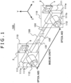
- Fig. 1 is a diagram illustrating a schematic configuration of an in-vehicle multiple-lens imaging apparatus 100 that is an example of an imaging apparatus.
- This multiple-lens imaging apparatus 100 includes two imaging modules 110 on both ends of a center body 130.
- the two imaging modules 110 are installed at positions at which optical axes thereof are generally parallel to each other and which are apart from each other by a predetermined distance (baseline length).
- the multiple-lens imaging apparatus 100 can determine a distance to an object from a parallax between images obtained from the two imaging modules 110.
- Module holders 111 of the imaging modules 110 are provided on both of the ends of the center body 130, respectively.
- Each module holder 111 includes a base section 111a and a cylindrical section 111b.
- a lens barrel 112 equipped with a lens is attached to the cylindrical section 111b.
- a substrate 2 on which an imaging element 5 and the like are loaded is fixed to a back surface of the lens barrel 112.
- the imaging element 5 is configured with a CCD, a CMOS, or the like.
- An image processing IC 131, a microcomputer 132, a connector 133, and the like are provided in the center body 130.
- the image processing IC 131 transmits and receives various control signals and analog imaging signals to and from each of the imaging modules 110, converts the received analog imaging signals into digital signals, and calculates a distance to an imaged object, a magnitude, and the like.
- the microcomputer 132 is a control circuit that controls the image processing IC 131.
- the connector 133 supplies electric power and outputs a picked-up image and the like processed by the image processing IC 131 to an external device.
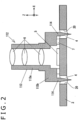
- Fig. 2 is a cross-sectional view illustrating the lens barrel 112 and the substrate 2 of each imaging module 110.
- the lens barrel 112 includes one or more lenses 6 and a holding section 113 that holds the lenses 6.
- the holding section 113 includes a cylindrical section 113a and a base section 113b provided with support pins 114.
- the support pins 114 may be formed either integrally with or separately from the base section 113b.
- a through-hole 20 into which each support pin 114 is inserted is formed in the substrate 2 on which the imaging element 5 is loaded.
- Each support pin 114 and the substrate 2 are fixed to each other by an adhesive 4 provided in the through-hole 20.
- an adhesive 4 an ultraviolet cure adhesive, for example, is used.
- each support pin 114 In work for adhesively fixing each support pin 114 to the substrate 2, the adhesive is coated to a portion in which the through-hole 20 is provided, a tip end of the support pin 114 is inserted into the through-hole 20, and a position of the lens barrel 112 relative to the substrate 2 is adjusted so that a focal point of each lens matches an imaging plane. In addition, after position adjustment, the portion in which the adhesive 4 is provided is irradiated with a UV ray to cure the adhesive 4.
- an adhesive 7 besides the adhesive 4 is provided to surround the imaging element 5 in such a manner as to seal a clearance between the base section 113b and the substrate 2.
- This adhesive 7 is additionally coated after curing the adhesive 4 and enables maintenance of strength and further improvement of reliability.
- the support pin 114 is characterized by a shape.
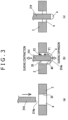
- a support pin 214 is a columnar pin and a tip end face 214a is planar.
- the support pin 214 is inserted into the through-hole 20.
- a UV ray is radiated to cure the adhesive 4.
- the support pin 214 is inserted into the through-hole 20 after the adhesive 4 is injected into the through-hole 20 without injecting the adhesive 4 into the through-hole 20 after inserting the support pin 214 into the through-hole 20 as in the conventional technique for the following reasons.
- a restricted work space for injection work makes it quite difficult to conduct the injection work. This entails an increase in a manufacturing cost.
- a clearance between the through-hole 20 and the support pin 114 is relatively small and the adhesive 4 relatively high in viscosity is injected into the clearance, the adhesive 4 can be injected only insufficiently and a cavity tends to be generated.
- a force indicated by arrows F1 and F2 is generated in an adhesive portion of the support pin 214 in a case in which the adhesive 4 contracts due to, for example, a reduction in an environmental temperature.
- the force becomes greater as the fillet 40 is larger, with the result that an amount of positional displacement of the support pin 214 in an axis direction grows and a problem of defocusing of an optical system occurs.
- the adhesive 4 is pushed out by the tip end face 214a and the fillet 40 is formed in such a way as to be dragged and tends to be larger.
- Fig. 4 is an illustrative diagram of the support pin 114 of the imaging module 110.
- a tip end portion 114a of the support pin 114 is tapered from a root side of the pin toward a tip end of the pin.
- the tip end portion 114a is of a conical shape narrower downward.
- an area of the tip end of the support pin 114 is smaller than that of the tip end of the support pin 214 illustrated in Fig. 3 ; thus, before a lower surface 42 of the adhesive 4 protrudes beyond a lower opening surface 20b of the through-hole 20, the tip end of the support pin 114 penetrates the adhesive 4.
- the shape of the support pin 114 illustrated in Fig. 4 is an example of the tapered shape from the root side of the pin to the tip end of the pin and the shape of the support pin 114 may be, for example, shapes as illustrated in Fig. 5 .
- the tip end of the tip end portion 114a is pointed.
- the tip end of the tip end portion 114a is planar. In this case, it is similarly possible to sufficiently reduce an area of a tip end face 114b, compared with the tip end face 214a of the columnar support pin 214 illustrated in Fig. 3 .
- the tip end of the support pin 114 easily penetrates the adhesive 4 and it is possible to prevent the tip end of the support pin 114 from being covered with the adhesive 4 as illustrated in Fig. 3(b) .
- the tip end of the support pin 114 penetrates the lower surface 42 of the adhesive 4 before the lower surface 42 largely protrudes downward; thus, it is possible to reduce the magnitude of the fillet 40, compared with a case of Fig. 3(b) .
- a height of the conical tip end portion 114a is reduced, compared with the case of Fig. 4 .
- an angle ⁇ of the tip end portion is larger than that of the tip end portion of the support pin 114 illustrated in Fig. 4 .
- the support pin 114 illustrated in Fig. 5(b) penetrates the adhesive 4 more easily than a columnar pin like the support pin 214; thus, it is similarly possible to prevent the tip end portion of the pin from being covered with the adhesive 4 and suppress the protrusion of the adhesive 4 from the opening surface 20b (refer to Fig. 4 ). As a result, it is possible to reduce axial movement of the support pin 114 in the case of expansion and contraction of the adhesive 4.
- the support pin 114 illustrated in Fig. 5(c) has a shape such that the tip end portion 114a of the columnar support pin 114 is obliquely cut.
- a cut surface 114c is oval.
- the tip end portion 114a is tapered toward a tip end and the support pin 114 penetrates the adhesive 4 easily. Owing to this, it is possible to prevent the adhesive 4 from being formed to cover the tip end portion of the pin with the adhesive 4, suppress the protrusion of the adhesive 4 from the opening surface 20b (refer to Fig. 4 ), and reduce the axial displacement of the support pin 114 accompanying expansion and contraction of the adhesive 4.
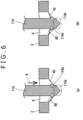
- Fig. 6 shows diagrams illustrating a modification of the support pin 114.
- the support pin 114 illustrated in Fig. 6 is obtained by forming a ring groove 114d in the support pin 114 illustrated in Fig. 5(b) .
- the tip end portion 114a penetrates the adhesive 4, the lower surface 42 of the adhesive 4 is turned into a state of being swollen downward, and the fillet 40 is formed.
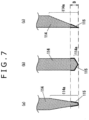
- Fig. 7 shows diagrams illustrating other modifications.
- Fig. 7 shows diagrams illustrating cross-sections of the support pin 114, and cross-sectional shapes of (a) to (d) correspond to cross-sectional shapes of the support pin 114 illustrated in (a) to (c) of Fig. 5 .
- a film 115 that prevents adhesion of the adhesive 4 is further formed in at least a portion of the tip end portion 114a including the tip end of the support pin 114.
- the film 115 is formed in a range indicated by a symbol B.
- any material that can repel the adhesive 4 can be used.
- an ordinary surface treatment such as coating, a plasma treatment, or an ozone treatment is considered to be available.
- the imaging module 110 includes: the substrate 2 on which the imaging element 5 is mounted and in which the through-hole 20 is formed; the holding section 113 that has the support pin 114 inserted into the through-hole 20 in such a manner that the support pin 114 penetrates the through-hole 20 and that holds the lenses 6 forming a subject image on the imaging element 5; and the adhesive 4 that is provided in the through-hole 20 and that fixes the substrate 2 to the support pin 114, and at least the tip end portion 114a of the support pin 114 has the tapered shape from the root side of the support pin 114 toward the tip end of the support pin 114.
- Forming the tip end portion 114a of the support pin 114 into the tapered shape smaller toward the tip end in this way makes it easy for the tip end portion 114a to penetrate the adhesive 4. It is thereby possible to avoid a situation in which a region including the tip end of the support pin 114 is covered with the adhesive 4 as illustrated in Fig. 3(b) , and reduce the fillet 40 of the adhesive 4 formed in a range from the support pin 114 to an edge of the through-hole 20. As a result, it is possible to reduce the axial movement of the support pin 114 due to expansion and contraction of the adhesive 4.
- the film (for example, fluororesin film) 115 that prevents the adhesion of the adhesive 4 in at least a portion including the tip end of the tip end portion 114a of the support pin 114. It is thereby possible to further enhance an effect of preventing the tip end of the support pin 114 from being covered with the adhesive 4 and reduce the axial movement of the support pin 114 due to expansion and contraction of the adhesive 4.
- the holding section 113 and the support pins 114 are formed integrally in the configuration illustrated in Fig. 2 , the holding section 113 and the support pins 114 may be formed separately. For example, integrally molding the holding section 113 and the support pin 114 by a resin or the like can contribute to cost reduction.
- configuring the imaging module 110, as illustrated in Fig. 2 , such that the adhesive 7 is provided in such a manner as to surround the imaging element 5 in a state in which the support pin 114 is inserted into the through-hole 20 and adhesively bonded to the substrate 2 as described above makes it possible to reduce the amount of the positional displacement of the support pin 114 in the axial direction after a reliability test and the amount of the temperature-dependent positional displacement in the axial direction.
- Fig. 8 is an illustrative diagram of a second embodiment and illustrates a fixing portion (adhesive portion) in which the support pin 114 is fixed (adhesively bonded) to the substrate 2. It is noted that a shape of the support pin 114 is similar to that illustrated in Fig. 5(b) . Owing to this, the tip end portion of the support pin 114 penetrates the lower surface 42 of the adhesive 4 and the tip end of the support pin 114 is not covered with the adhesive 4. Furthermore, in an example illustrated in Fig. 8 , the adhesive 4 not only protrudes downward from the lower opening surface 20b in Fig. 8 but also protrudes upward from an upper opening surface 20a in Fig. 8 .
- fillets 40a and 40b are formed outside of the opening surfaces 20a and 20b.
- comparing a contact area S1 of the adhesive 4 on an outer peripheral surface of the support pin 114 with a projection area S2 in a case of projecting a cross-section of the substrate 2 onto the outer peripheral surface of the support pin 114 leads to S1 > S2.
- the adhesive 4 spreads outside of a region put between the opening surfaces 20a and 20b with respect to the support pin 114, an adhesive area increases and the adhesive strength grows.
- the higher adhesive strength enables an increase in resistance to temperature, humidity, and impact, thereby making it possible to ensure long-term reliability.
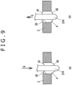
- Fig. 9 illustrates an example of a method of forming an adhesive shape as illustrated in Fig. 8 .
- the adhesive 4 is disposed in the through-hole 20 of the substrate 2.
- the support pin 114 is inserted into the through-hole 20 in an arrow D direction and the support pin 114 is moved downward until the tip end portion of the support pin 114 penetrates the lower surface 42 of the adhesive 4.
- the upper surface 41 of the adhesive 4 has a shape recessed in the through-hole 20 while the lower surface 42 has a shape protruding downward from the through-hole 20.
- the support pin 114 is moved in a direction of pulling out the support pin 114, that is, an arrow E direction.
- the adhesive 4 is then dragged upward in Fig. 9(b) , the upper surface 41 protrudes upward from the through-hole 20, and an amount of protrusion of the lower surface 42 decreases.
- a position of the lens barrel 112 in x-axis and y-axis directions and a position thereof in a z-axis direction (optical axis direction) in Fig. 2 are adjusted for optical axis alignment between the optical system and the imaging element 5 and focus adjustment.
- the support pin 114 is inserted into the through-hole 20 in such a manner as to penetrate the through-hole 20 from one opening surface 20a to the other opening surface 20b, one portion of the adhesive 4 provided in the through-hole 20 protrudes outside of the through-hole beyond the opening surface 20a, and another portion thereof protrudes outside of the through-hole beyond the opening surface 20b.
- the direction of the force acting on the support pin 114 from the adhesive 4 provided on the opening surface 20a side is opposite to the direction of the force acting on the support pin 114 from the adhesive 4 provided on the opening surface 20b side.
Landscapes
- Physics & Mathematics (AREA)
- General Physics & Mathematics (AREA)
- Optics & Photonics (AREA)
- Engineering & Computer Science (AREA)
- Multimedia (AREA)
- Signal Processing (AREA)
- Studio Devices (AREA)
- Transforming Light Signals Into Electric Signals (AREA)
- Camera Bodies And Camera Details Or Accessories (AREA)
- Lens Barrels (AREA)
Description
- The present invention relates to an imaging module and an imaging apparatus.
- As a configuration of an in-vehicle imaging apparatus including an imaging module, a configuration disclosed in, for example, Patent Document 1 is known. An imaging module disclosed in Patent Document 1 includes an imaging substrate on which an imaging element that converts light into an electrical signal is mounted and which has a through-hole; a lens member that condenses subject light on the imaging element; and a support pin that is bonded to the imaging substrate and to the lens member in a state of being inserted into the through-hole, and that fixes the imaging substrate to the lens member in an overlapping state at a predetermined gap kept between the lens member and the imaging substrate. Patent Document 1 also discloses that the support pin is bonded to the imaging substrate by a solder and that an adhesive such as a resin is also used for bonding the support pin.
- Patent Document 1:
JP-2007-174358-A -
US 5 359 190 A discloses an imaging module with the features in the preamble of present claim 1. - However, with the configuration such that the support pin that is being inserted into the through-hole is bonded to the imaging substrate by the adhesive, unevenness in a coating shape of the adhesive causes expansion and contraction of the adhesive due to a temperature change or the like, possibly resulting in optical axis misalignment.
- An imaging module according to a first aspect of the present invention includes the features defined in claim 1.
- According to the present invention, it is possible to reduce defocusing caused by expansion and contraction of the adhesive.
-
-
Fig. 1 is a diagram illustrating a schematic configuration of a multiple-lens imaging apparatus. -
Fig. 2 is a cross-sectional view of an imaging module. -
Fig. 3 shows illustrative diagrams of a comparison. -
Fig. 4 is an illustrative diagram of a support pin according to a first embodiment. -
Fig. 5 shows diagrams illustrating other examples of a shape of the support pin. -
Fig. 6 shows diagrams illustrating a modification of the support pin. -
Fig. 7 shows diagrams illustrating other modifications of the support pin. -
Fig. 8 is an illustrative diagram of a second embodiment. -
Fig. 9 shows diagrams illustrating an example of a method of forming an adhesive shape. - Embodiments of the present invention will be described hereinafter with reference to the drawings.
-
Fig. 1 is a diagram illustrating a schematic configuration of an in-vehicle multiple-lens imaging apparatus 100 that is an example of an imaging apparatus. This multiple-lens imaging apparatus 100 includes twoimaging modules 110 on both ends of acenter body 130. The twoimaging modules 110 are installed at positions at which optical axes thereof are generally parallel to each other and which are apart from each other by a predetermined distance (baseline length). The multiple-lens imaging apparatus 100 can determine a distance to an object from a parallax between images obtained from the twoimaging modules 110. -
Module holders 111 of theimaging modules 110 are provided on both of the ends of thecenter body 130, respectively. Eachmodule holder 111 includes abase section 111a and acylindrical section 111b. Alens barrel 112 equipped with a lens is attached to thecylindrical section 111b. Asubstrate 2 on which animaging element 5 and the like are loaded is fixed to a back surface of thelens barrel 112. Theimaging element 5 is configured with a CCD, a CMOS, or the like. - An
image processing IC 131, amicrocomputer 132, aconnector 133, and the like are provided in thecenter body 130. Theimage processing IC 131 transmits and receives various control signals and analog imaging signals to and from each of theimaging modules 110, converts the received analog imaging signals into digital signals, and calculates a distance to an imaged object, a magnitude, and the like. Themicrocomputer 132 is a control circuit that controls theimage processing IC 131. Theconnector 133 supplies electric power and outputs a picked-up image and the like processed by theimage processing IC 131 to an external device. -
Fig. 2 is a cross-sectional view illustrating thelens barrel 112 and thesubstrate 2 of eachimaging module 110. Thelens barrel 112 includes one ormore lenses 6 and aholding section 113 that holds thelenses 6. Theholding section 113 includes acylindrical section 113a and abase section 113b provided withsupport pins 114. Thesupport pins 114 may be formed either integrally with or separately from thebase section 113b. A through-hole 20 into which eachsupport pin 114 is inserted is formed in thesubstrate 2 on which theimaging element 5 is loaded. Eachsupport pin 114 and thesubstrate 2 are fixed to each other by an adhesive 4 provided in the through-hole 20. As the adhesive 4, an ultraviolet cure adhesive, for example, is used. - In work for adhesively fixing each
support pin 114 to thesubstrate 2, the adhesive is coated to a portion in which the through-hole 20 is provided, a tip end of thesupport pin 114 is inserted into the through-hole 20, and a position of thelens barrel 112 relative to thesubstrate 2 is adjusted so that a focal point of each lens matches an imaging plane. In addition, after position adjustment, the portion in which the adhesive 4 is provided is irradiated with a UV ray to cure the adhesive 4. - It is noted that in an example illustrated in
Fig. 2 , anadhesive 7 besides the adhesive 4 is provided to surround theimaging element 5 in such a manner as to seal a clearance between thebase section 113b and thesubstrate 2. Thisadhesive 7 is additionally coated after curing the adhesive 4 and enables maintenance of strength and further improvement of reliability. - In the embodiment illustrated in
Fig. 2 , thesupport pin 114 is characterized by a shape. First, conventional problems will be described with reference to a comparison ofFig. 3 . Normally, in a case of a conventional imaging module, asupport pin 214 is a columnar pin and atip end face 214a is planar. In the present embodiment, after disposing the adhesive in the through-hole 20 of thesubstrate 2, thesupport pin 214 is inserted into the through-hole 20. In addition, a UV ray is radiated to cure the adhesive 4. - The
support pin 214 is inserted into the through-hole 20 after the adhesive 4 is injected into the through-hole 20 without injecting the adhesive 4 into the through-hole 20 after inserting thesupport pin 214 into the through-hole 20 as in the conventional technique for the following reasons. With a configuration such that the adhesive 4 is injected into the through-hole 20 after inserting thesupport pin 214 into the through-hole 20, a restricted work space for injection work makes it quite difficult to conduct the injection work. This entails an increase in a manufacturing cost. Furthermore, since a clearance between the through-hole 20 and thesupport pin 114 is relatively small and the adhesive 4 relatively high in viscosity is injected into the clearance, the adhesive 4 can be injected only insufficiently and a cavity tends to be generated. - In a case of inserting the
support pin 214 into the through-hole 20 after disposing the adhesive 4 in the through-hole 20 in this way and atip end face 214a of thecolumnar support pin 214 is flat, then the adhesive within the through-hole 20 is pushed out by thetip end face 214a of thesupport pin 214 as illustrated inFig. 3(b) , and the adhesive 4 around thetip end face 214 is swollen on a rear side in such a way of being dragged. In other words, the adhesive 4 adheres to an entire tip end of the pin. As a result, afillet 40 of the adhesive 4 is formed between thesupport pin 214 and the through-hole 20. Furthermore, as illustrated inFig. 3(c) , in a case in which thesupport pin 214 penetrates the portion in which the adhesive 4 is provided, then the adhesive 4 in a large quantity adheres onto thetip end face 214a, resulting in something of insufficiency of the adhesive 4 within the through-hole 20. - After the
fillet 40 of the adhesive 4 is formed as illustrated inFig. 3(b) , a force indicated by arrows F1 and F2 is generated in an adhesive portion of thesupport pin 214 in a case in which the adhesive 4 contracts due to, for example, a reduction in an environmental temperature. The force becomes greater as thefillet 40 is larger, with the result that an amount of positional displacement of thesupport pin 214 in an axis direction grows and a problem of defocusing of an optical system occurs. In a case of a flat tip end as in thesupport pin 214, the adhesive 4 is pushed out by thetip end face 214a and thefillet 40 is formed in such a way as to be dragged and tends to be larger. Particularly if the adhesive 4 protrudes in such a way that a tip end portion of thesupport pin 214 is covered with the adhesive 4 as illustrated inFig. 3(b) , an amount of upward movement of thesupport pin 214 grows. Such movement of thesupport pin 114 also occurs when the adhesive 4 is cured. Conversely, in a case of expansion of the adhesive 4 due to an increase in the environmental temperature, a force opposite in direction to that in the case of contraction is generated to cause positional displacement of thelenses 6 in a direction of approaching theimaging element 5. - On the other hand, in a case illustrated in
Fig. 3(c) , an amount of the adhesive within the through-hole 20 decreases. As a result, there is a possibility that it is impossible to ensure an adhesive strength and to maintain reliability and that minute motions of the lenses resulting from the low strength cause optical axis misalignment. -
Fig. 4 is an illustrative diagram of thesupport pin 114 of theimaging module 110. Atip end portion 114a of thesupport pin 114 is tapered from a root side of the pin toward a tip end of the pin. Specifically, thetip end portion 114a is of a conical shape narrower downward. Owing to this, an area of the tip end of thesupport pin 114 is smaller than that of the tip end of thesupport pin 214 illustrated inFig. 3 ; thus, before alower surface 42 of the adhesive 4 protrudes beyond alower opening surface 20b of the through-hole 20, the tip end of thesupport pin 114 penetrates the adhesive 4. - As a result, it is possible to prevent the adhesive 4 from protruding to cover the tip end portion of the
support pin 114 with the adhesive 4. It is also possible to suppress protrusion of thelower surface 42 of the adhesive 4 from the openingsurface 20b, that is, reduce a magnitude of thefillet 40. As a result, a degree of dragging anupper surface 41 of the adhesive 4 into the through-hole 20 is also lowered. Therefore, it is possible to reduce an amount of movement of thesupport pin 114 either downward or upward inFig. 4 due to expansion and contraction of the adhesive 4, compared with the conventional technique. The expansion and contraction of the adhesive occur due to a temperature change or a humidity change. However, providing a structure as illustrated inFig. 4 makes it possible to reduce the amount of movement due to the temperature change or the humidity change; thus, even in a case in which a temperature of a product itself rises when the products operates, it is possible to suppress positional displacement of thesupport pin 114 in the adhesive portion. In other words, temperature characteristics of the product improve. - The shape of the
support pin 114 illustrated inFig. 4 is an example of the tapered shape from the root side of the pin to the tip end of the pin and the shape of thesupport pin 114 may be, for example, shapes as illustrated inFig. 5 . In a case of thesupport pin 114 illustrated inFig. 4 described above, the tip end of thetip end portion 114a is pointed. In a case of thesupport pin 114 illustrated inFig. 5(a) , the tip end of thetip end portion 114a is planar. In this case, it is similarly possible to sufficiently reduce an area of atip end face 114b, compared with thetip end face 214a of thecolumnar support pin 214 illustrated inFig. 3 . As a result, the tip end of thesupport pin 114 easily penetrates the adhesive 4 and it is possible to prevent the tip end of thesupport pin 114 from being covered with the adhesive 4 as illustrated inFig. 3(b) . Moreover, the tip end of thesupport pin 114 penetrates thelower surface 42 of the adhesive 4 before thelower surface 42 largely protrudes downward; thus, it is possible to reduce the magnitude of thefillet 40, compared with a case ofFig. 3(b) . As a result, it is possible to suppress axial displacement of thesupport pin 114 in the case of expansion and contraction of the adhesive 4. - In a case of the
support pin 114 illustrated inFig. 5(b) , a height of the conicaltip end portion 114a is reduced, compared with the case ofFig. 4 . In this case, an angle α of the tip end portion is larger than that of the tip end portion of thesupport pin 114 illustrated inFig. 4 . However, thesupport pin 114 illustrated inFig. 5(b) penetrates the adhesive 4 more easily than a columnar pin like thesupport pin 214; thus, it is similarly possible to prevent the tip end portion of the pin from being covered with the adhesive 4 and suppress the protrusion of the adhesive 4 from the openingsurface 20b (refer toFig. 4 ). As a result, it is possible to reduce axial movement of thesupport pin 114 in the case of expansion and contraction of the adhesive 4. - The
support pin 114 illustrated inFig. 5(c) has a shape such that thetip end portion 114a of thecolumnar support pin 114 is obliquely cut. Acut surface 114c is oval. In this case like above, thetip end portion 114a is tapered toward a tip end and thesupport pin 114 penetrates the adhesive 4 easily. Owing to this, it is possible to prevent the adhesive 4 from being formed to cover the tip end portion of the pin with the adhesive 4, suppress the protrusion of the adhesive 4 from the openingsurface 20b (refer toFig. 4 ), and reduce the axial displacement of thesupport pin 114 accompanying expansion and contraction of the adhesive 4. -
Fig. 6 shows diagrams illustrating a modification of thesupport pin 114. Thesupport pin 114 illustrated inFig. 6 is obtained by forming aring groove 114d in thesupport pin 114 illustrated inFig. 5(b) . When thesupport pin 114 is pushed down in the figure as indicated by an arrow A, then thetip end portion 114a penetrates the adhesive 4, thelower surface 42 of the adhesive 4 is turned into a state of being swollen downward, and thefillet 40 is formed. - When the
support pin 114 is pushed down further from this state, a force to return upward while being dragged downward acts on a portion in which thefillet 40 is formed. At this time, if thegroove 114d is formed on a peripheral surface of thesupport pin 114, a diameter is sharply reduced in this portion; thus, a force of the adhesive to adhere to thesupport pin 114 weakens and thelower surface 42 is easier to move upward as illustrated inFig. 6(b) . As a result, the portion in which thefillet 40 is formed is made smaller and it is possible to suppress the axial movement of thesupport pin 114 at the time of expansion and contraction of the adhesive 4. -
Fig. 7 shows diagrams illustrating other modifications.Fig. 7 shows diagrams illustrating cross-sections of thesupport pin 114, and cross-sectional shapes of (a) to (d) correspond to cross-sectional shapes of thesupport pin 114 illustrated in (a) to (c) ofFig. 5 . In the modification illustrated inFig. 7 , afilm 115 that prevents adhesion of the adhesive 4 is further formed in at least a portion of thetip end portion 114a including the tip end of thesupport pin 114. In examples ofFig. 7 , thefilm 115 is formed in a range indicated by a symbol B. - In this way, forming the
film 115 made of a low wettability substance that prevents the adhesion of the adhesive 4 in the range B makes it difficult for the adhesive 4 to adhere to this portion. As a result, it is possible to further reduce the magnitude of thefillet 40 illustrated inFig. 4 and suppress the axial movement of thesupport pin 114 accompanying expansion and contraction of the adhesive 4. - While various types of materials may be used for the
film 115 and examples of the materials include a fluororesin, an acrylic resin, a urethane resin, and a melamine resin, any material that can repel the adhesive 4 can be used. Furthermore, as a method of forming thefilm 115, an ordinary surface treatment such as coating, a plasma treatment, or an ozone treatment is considered to be available. - As described above, according to the first embodiment, the
imaging module 110 includes: thesubstrate 2 on which theimaging element 5 is mounted and in which the through-hole 20 is formed; the holdingsection 113 that has thesupport pin 114 inserted into the through-hole 20 in such a manner that thesupport pin 114 penetrates the through-hole 20 and that holds thelenses 6 forming a subject image on theimaging element 5; and the adhesive 4 that is provided in the through-hole 20 and that fixes thesubstrate 2 to thesupport pin 114, and at least thetip end portion 114a of thesupport pin 114 has the tapered shape from the root side of thesupport pin 114 toward the tip end of thesupport pin 114. - Forming the
tip end portion 114a of thesupport pin 114 into the tapered shape smaller toward the tip end in this way makes it easy for thetip end portion 114a to penetrate the adhesive 4. It is thereby possible to avoid a situation in which a region including the tip end of thesupport pin 114 is covered with the adhesive 4 as illustrated inFig. 3(b) , and reduce thefillet 40 of the adhesive 4 formed in a range from thesupport pin 114 to an edge of the through-hole 20. As a result, it is possible to reduce the axial movement of thesupport pin 114 due to expansion and contraction of the adhesive 4. - Moreover, as illustrated in
Fig. 7 , it is preferable to form the film (for example, fluororesin film) 115 that prevents the adhesion of the adhesive 4 in at least a portion including the tip end of thetip end portion 114a of thesupport pin 114. It is thereby possible to further enhance an effect of preventing the tip end of thesupport pin 114 from being covered with the adhesive 4 and reduce the axial movement of thesupport pin 114 due to expansion and contraction of the adhesive 4. - Furthermore, while the holding
section 113 and the support pins 114 are formed integrally in the configuration illustrated inFig. 2 , the holdingsection 113 and the support pins 114 may be formed separately. For example, integrally molding the holdingsection 113 and thesupport pin 114 by a resin or the like can contribute to cost reduction. - It is noted that configuring the
imaging module 110, as illustrated inFig. 2 , such that the adhesive 7 is provided in such a manner as to surround theimaging element 5 in a state in which thesupport pin 114 is inserted into the through-hole 20 and adhesively bonded to thesubstrate 2 as described above makes it possible to reduce the amount of the positional displacement of thesupport pin 114 in the axial direction after a reliability test and the amount of the temperature-dependent positional displacement in the axial direction. Moreover, even in a case in which the position of thesupport pin 114 is displaced from a center of the through-hole 20 at a time of curing the adhesive 4, not only adhesive bonding to thesubstrate 2 using thesupport pin 114 but also use of the adhesive 7 makes it possible to suppress the positional displacement of thesupport pin 114 in a substrate planar direction or the axial direction; thus, the temperature characteristics and the positional displacement after the reliability test are not affected. -
Fig. 8 is an illustrative diagram of a second embodiment and illustrates a fixing portion (adhesive portion) in which thesupport pin 114 is fixed (adhesively bonded) to thesubstrate 2. It is noted that a shape of thesupport pin 114 is similar to that illustrated inFig. 5(b) . Owing to this, the tip end portion of thesupport pin 114 penetrates thelower surface 42 of the adhesive 4 and the tip end of thesupport pin 114 is not covered with the adhesive 4. Furthermore, in an example illustrated inFig. 8 , the adhesive 4 not only protrudes downward from thelower opening surface 20b inFig. 8 but also protrudes upward from anupper opening surface 20a inFig. 8 . In other words,fillets support pin 114 with a projection area S2 in a case of projecting a cross-section of thesubstrate 2 onto the outer peripheral surface of thesupport pin 114 leads to S1 > S2. - As described above, with the presence of the
fillets fillets Fig. 8 , in a case of contraction of the adhesive 4, a direction a force F3 of thelower fillet 40b is an upward direction inFig. 8 and that of a force F4 of thefillet 40a is a downward direction inFig. 8 . On the other hand, in a case of expansion of the adhesive 4, the directions of the forces are reversed. In either case, the forces F3 and F4 are in the directions in which the forces F3 and F4 cancel each other; thus, it is possible to reduce the axial movement of thesupport pin 114 in the case of expansion and contraction of the adhesive 4. For example, when magnitudes of thefillets - Moreover, since the adhesive 4 spreads outside of a region put between the opening surfaces 20a and 20b with respect to the
support pin 114, an adhesive area increases and the adhesive strength grows. The higher adhesive strength enables an increase in resistance to temperature, humidity, and impact, thereby making it possible to ensure long-term reliability. -
Fig. 9 illustrates an example of a method of forming an adhesive shape as illustrated inFig. 8 . First, the adhesive 4 is disposed in the through-hole 20 of thesubstrate 2. Next, as illustrated inFig. 9(a) , thesupport pin 114 is inserted into the through-hole 20 in an arrow D direction and thesupport pin 114 is moved downward until the tip end portion of thesupport pin 114 penetrates thelower surface 42 of the adhesive 4. At this time, theupper surface 41 of the adhesive 4 has a shape recessed in the through-hole 20 while thelower surface 42 has a shape protruding downward from the through-hole 20. - Next, as illustrated in
Fig. 9(b) , thesupport pin 114 is moved in a direction of pulling out thesupport pin 114, that is, an arrow E direction. The adhesive 4 is then dragged upward inFig. 9(b) , theupper surface 41 protrudes upward from the through-hole 20, and an amount of protrusion of thelower surface 42 decreases. Subsequently, a position of thelens barrel 112 in x-axis and y-axis directions and a position thereof in a z-axis direction (optical axis direction) inFig. 2 are adjusted for optical axis alignment between the optical system and theimaging element 5 and focus adjustment. - As described so far, according to the second embodiment, as illustrated in
Fig. 8 , thesupport pin 114 is inserted into the through-hole 20 in such a manner as to penetrate the through-hole 20 from oneopening surface 20a to the other openingsurface 20b, one portion of the adhesive 4 provided in the through-hole 20 protrudes outside of the through-hole beyond the openingsurface 20a, and another portion thereof protrudes outside of the through-hole beyond the openingsurface 20b. Owing to this, during expansion and contraction of the adhesive 4, the direction of the force acting on thesupport pin 114 from the adhesive 4 provided on theopening surface 20a side is opposite to the direction of the force acting on thesupport pin 114 from the adhesive 4 provided on theopening surface 20b side. As a result, it is possible to reduce the movement of thesupport pin 114 in the optical axis direction accompanying expansion and contraction of the adhesive 4. - While various embodiments and various modifications have been described above, the present invention is not limited to contents of these embodiments and modifications. Other possible aspects within the scope of the technical concept of the present invention are also contained in the scope of the present invention.
- The present application claims the priority of:
Japanese Patent Application No. 2016-089030 (filed April 27, 2016 -
- 4, 7: Adhesive
- 5: Imaging element
- 6: Lens
- 40, 40a, 40b: Fillet
- 100: Multiple-lens imaging apparatus
- 110: Imaging module
- 112: Lens barrel
- 113: Holding section
- 114, 214: Support pin
- 114a: Tip end portion
- 115: Film
Claims (6)
- An imaging module (110) comprising:a substrate (2) on which an imaging element (5) is mounted and in which a through-hole (20) is formed;a holding section (113) that has a support pin (114) inserted into the through-hole (20) in such a manner as to penetrate the through-hole (20), and that holds an optical system forming a subject image on the imaging element (5); andan adhesive (4) that is provided in the through-hole (20) and that fixes the substrate (2) to the support pin (114), whereinat least a tip end portion (114a) of the support pin (114) is of a tapered shape from a root side of the support pin (114) toward a tip end of the support pin (114),characterised in that the tip end of the support pin (114) penetrates the adhesive (4) so that it is not covered by the adhesive (4).
- The imaging module (110) according to claim 1, whereinthe support pin (114) is inserted into the through-hole (20) in such a manner as to penetrate the through-hole (20) from a first opening surface (20a) that is one of opening surfaces to a second opening surface (20b) that is other opening surface, andone portion of the adhesive (4) provided in the through-hole (20) protrudes outside of the through-hole (20) beyond the first opening surface (20a), and another portion of the adhesive (4) protrudes outside of the through-hole (20) beyond the second opening surface (20b).
- The imaging module (110) according to claim 1, further comprising an adhesive (7) that is disposed around the imaging element (5) and that fixes the holding section (113) to the substrate (2).
- The imaging module (110) according to claim 1, wherein a film (115) that prevents adhesion of the adhesive (4) is formed in at least a portion including a tip end of the tip end portion (114a).
- The imaging module (110) according to claim 1, wherein the holding section (113) and the support pin (114) are formed integrally by a resin.
- An imaging apparatus (100) including the imaging module (110) according to any one of claims 1 to 5.
Applications Claiming Priority (2)
| Application Number | Priority Date | Filing Date | Title |
|---|---|---|---|
| JP2016089030A JP6630226B2 (en) | 2016-04-27 | 2016-04-27 | Imaging module and imaging device |
| PCT/JP2017/015165 WO2017188013A1 (en) | 2016-04-27 | 2017-04-13 | Image pickup module and image pickup device |
Publications (3)
| Publication Number | Publication Date |
|---|---|
| EP3451647A1 EP3451647A1 (en) | 2019-03-06 |
| EP3451647A4 EP3451647A4 (en) | 2019-12-18 |
| EP3451647B1 true EP3451647B1 (en) | 2023-08-09 |
Family
ID=60160485
Family Applications (1)
| Application Number | Title | Priority Date | Filing Date |
|---|---|---|---|
| EP17789299.9A Active EP3451647B1 (en) | 2016-04-27 | 2017-04-13 | Image pickup module and image pickup device |
Country Status (5)
| Country | Link |
|---|---|
| US (1) | US11418686B2 (en) |
| EP (1) | EP3451647B1 (en) |
| JP (1) | JP6630226B2 (en) |
| CN (1) | CN109076153B (en) |
| WO (1) | WO2017188013A1 (en) |
Families Citing this family (3)
| Publication number | Priority date | Publication date | Assignee | Title |
|---|---|---|---|---|
| JP6941686B2 (en) * | 2017-11-07 | 2021-09-29 | 日立Astemo株式会社 | In-vehicle imaging device |
| WO2020240968A1 (en) * | 2019-05-24 | 2020-12-03 | 三菱電機株式会社 | Method and device for manufacturing camera module, and method for manufacturing optical module |
| JP2024070005A (en) * | 2022-11-10 | 2024-05-22 | 日立Astemo株式会社 | Vehicle-mounted camera device and method for manufacturing the vehicle-mounted camera device |
Family Cites Families (21)
| Publication number | Priority date | Publication date | Assignee | Title |
|---|---|---|---|---|
| JPS6441383A (en) * | 1987-08-07 | 1989-02-13 | Canon Kk | Image pickup element fixing device |
| US5359190A (en) * | 1992-12-31 | 1994-10-25 | Apple Computer, Inc. | Method and apparatus for coupling an optical lens to an imaging electronics array |
| JP4033439B2 (en) * | 2001-09-11 | 2008-01-16 | シャープ株式会社 | Solid-state imaging unit, manufacturing method thereof, and imaging device |
| JP4154223B2 (en) * | 2002-12-18 | 2008-09-24 | キヤノン株式会社 | LENS DEVICE AND IMAGING DEVICE |
| TW579169U (en) * | 2003-05-28 | 2004-03-01 | Benq Corp | Optical module for a digital camera |
| CN101102409A (en) * | 2003-07-08 | 2008-01-09 | 柯尼卡美能达精密光学株式会社 | Imaging device, portable terminal with the same and manufacturing method for the imaging device |
| US20050041098A1 (en) * | 2003-08-18 | 2005-02-24 | Inventec Micro-Electronics Corporation | Digital image capturing module assembly and method of fabricating the same |
| US20050052568A1 (en) * | 2003-09-10 | 2005-03-10 | Inventec Micro-Electronics Corporation | Digital image capturing module assembly and method of fabricating the same |
| JP2006098497A (en) * | 2004-09-28 | 2006-04-13 | Nikon Corp | Optical module |
| US7469100B2 (en) * | 2005-10-03 | 2008-12-23 | Flextronics Ap Llc | Micro camera module with discrete manual focal positions |
| JP4761956B2 (en) * | 2005-12-22 | 2011-08-31 | 京セラ株式会社 | Imaging module and imaging apparatus |
| JP4492533B2 (en) | 2005-12-27 | 2010-06-30 | 船井電機株式会社 | Compound eye imaging device |
| JP2008092417A (en) * | 2006-10-04 | 2008-04-17 | Matsushita Electric Ind Co Ltd | Semiconductor imaging device, method for manufacturing the same, semiconductor imaging device, and semiconductor imaging module |
| CN101578853B (en) * | 2007-01-05 | 2012-11-28 | 株式会社理光 | Imaging apparatus and electronic device |
| CN101750695A (en) * | 2008-12-01 | 2010-06-23 | 深圳富泰宏精密工业有限公司 | Portable electronic device |
| CN201364448Y (en) * | 2009-02-19 | 2009-12-16 | 广达电脑股份有限公司 | Camera shooting assembly |
| CN103826052A (en) * | 2009-02-23 | 2014-05-28 | 京瓷株式会社 | Imaging module |
| TW201123857A (en) * | 2009-12-25 | 2011-07-01 | Hon Hai Prec Ind Co Ltd | Camera module |
| JP2012252308A (en) * | 2011-06-07 | 2012-12-20 | Enplas Corp | Optical receptacle, and optical module with the same |
| JPWO2014034360A1 (en) * | 2012-08-31 | 2016-08-08 | シャープ株式会社 | Lens driving device and camera module |
| JP6638151B2 (en) * | 2014-07-04 | 2020-01-29 | 日本電産コパル株式会社 | Imaging device |
-
2016
- 2016-04-27 JP JP2016089030A patent/JP6630226B2/en active Active
-
2017
- 2017-04-13 US US16/097,094 patent/US11418686B2/en active Active
- 2017-04-13 EP EP17789299.9A patent/EP3451647B1/en active Active
- 2017-04-13 WO PCT/JP2017/015165 patent/WO2017188013A1/en not_active Ceased
- 2017-04-13 CN CN201780026075.9A patent/CN109076153B/en active Active
Also Published As
| Publication number | Publication date |
|---|---|
| JP2017200039A (en) | 2017-11-02 |
| WO2017188013A1 (en) | 2017-11-02 |
| JP6630226B2 (en) | 2020-01-15 |
| CN109076153B (en) | 2020-12-01 |
| EP3451647A1 (en) | 2019-03-06 |
| US20210227108A1 (en) | 2021-07-22 |
| CN109076153A (en) | 2018-12-21 |
| EP3451647A4 (en) | 2019-12-18 |
| US11418686B2 (en) | 2022-08-16 |
Similar Documents
| Publication | Publication Date | Title |
|---|---|---|
| JP5617561B2 (en) | Imaging device | |
| CN104871083B (en) | Imager module and method for manufacturing imager module | |
| US9848757B2 (en) | Endoscope and endoscope system | |
| CN101406039B (en) | Method for assembling a camera module, and camera module | |
| JP5771901B2 (en) | Imaging device | |
| EP2680059B1 (en) | A pickup imaging assembly, endoscope, and method of manufacturing a pickup imaging assembly | |
| US10104275B2 (en) | Manufacturing method for camera module, and camera module | |
| US11418686B2 (en) | Image pickup module and image pickup device | |
| US10288985B2 (en) | Imaging device, optical device, electronic device, vehicle, and production method for imaging device | |
| KR102119329B1 (en) | Lens device, camera, vehicle and method for automotive cameras with improved adhesion area | |
| JP2016027360A (en) | Imaging device | |
| EP3002619B1 (en) | Method for assembling a camera | |
| US20170052385A1 (en) | Lens focusing method and optical module | |
| CN112492133A (en) | Method of joining camera lenses, joining element and camera lens assembly | |
| GB2554110A (en) | Camera module for a vehicle | |
| EP3226050A1 (en) | Imaging apparatus | |
| US20120175508A1 (en) | Sensor module | |
| CN106646808B (en) | Camera model | |
| EP2476542A2 (en) | Method of manufacturing lens and lens manufactured using the same | |
| EP3291529A1 (en) | Camera module for a motor vehicle and method for producing a camera module | |
| CN114080554B (en) | Lens mount and flange design for camera modules | |
| US11453177B2 (en) | Welding assembly and method for producing a welding assembly | |
| US12529941B2 (en) | Camera module | |
| EP2538254A1 (en) | Optical communication component and method for manufacturing the same | |
| PH12016000398A1 (en) | An optimally aligned camera module with perfect camera axis alignment to fixation and secure lens binding |
Legal Events
| Date | Code | Title | Description |
|---|---|---|---|
| STAA | Information on the status of an ep patent application or granted ep patent |
Free format text: STATUS: THE INTERNATIONAL PUBLICATION HAS BEEN MADE |
|
| PUAI | Public reference made under article 153(3) epc to a published international application that has entered the european phase |
Free format text: ORIGINAL CODE: 0009012 |
|
| STAA | Information on the status of an ep patent application or granted ep patent |
Free format text: STATUS: REQUEST FOR EXAMINATION WAS MADE |
|
| 17P | Request for examination filed |
Effective date: 20181026 |
|
| AK | Designated contracting states |
Kind code of ref document: A1 Designated state(s): AL AT BE BG CH CY CZ DE DK EE ES FI FR GB GR HR HU IE IS IT LI LT LU LV MC MK MT NL NO PL PT RO RS SE SI SK SM TR |
|
| AX | Request for extension of the european patent |
Extension state: BA ME |
|
| DAV | Request for validation of the european patent (deleted) | ||
| DAX | Request for extension of the european patent (deleted) | ||
| A4 | Supplementary search report drawn up and despatched |
Effective date: 20191120 |
|
| RIC1 | Information provided on ipc code assigned before grant |
Ipc: G02B 7/02 20060101ALI20191114BHEP Ipc: H04N 5/225 20060101AFI20191114BHEP Ipc: G02B 27/62 20060101ALI20191114BHEP Ipc: G03B 17/02 20060101ALI20191114BHEP Ipc: G02B 7/00 20060101ALI20191114BHEP |
|
| STAA | Information on the status of an ep patent application or granted ep patent |
Free format text: STATUS: EXAMINATION IS IN PROGRESS |
|
| 17Q | First examination report despatched |
Effective date: 20210430 |
|
| RAP3 | Party data changed (applicant data changed or rights of an application transferred) |
Owner name: HITACHI ASTEMO, LTD. |
|
| REG | Reference to a national code |
Ref country code: DE Ref legal event code: R079 Free format text: PREVIOUS MAIN CLASS: H04N0005225000 Ipc: H04N0023000000 Ref country code: DE Ref legal event code: R079 Ref document number: 602017072504 Country of ref document: DE Free format text: PREVIOUS MAIN CLASS: H04N0005225000 Ipc: H04N0023000000 |
|
| GRAP | Despatch of communication of intention to grant a patent |
Free format text: ORIGINAL CODE: EPIDOSNIGR1 |
|
| STAA | Information on the status of an ep patent application or granted ep patent |
Free format text: STATUS: GRANT OF PATENT IS INTENDED |
|
| RIC1 | Information provided on ipc code assigned before grant |
Ipc: G02B 7/00 20060101ALI20230201BHEP Ipc: G02B 27/62 20060101ALI20230201BHEP Ipc: G03B 17/02 20060101ALI20230201BHEP Ipc: G02B 7/02 20060101ALI20230201BHEP Ipc: H04N 23/00 20230101AFI20230201BHEP |
|
| INTG | Intention to grant announced |
Effective date: 20230224 |
|
| GRAS | Grant fee paid |
Free format text: ORIGINAL CODE: EPIDOSNIGR3 |
|
| GRAA | (expected) grant |
Free format text: ORIGINAL CODE: 0009210 |
|
| STAA | Information on the status of an ep patent application or granted ep patent |
Free format text: STATUS: THE PATENT HAS BEEN GRANTED |
|
| AK | Designated contracting states |
Kind code of ref document: B1 Designated state(s): AL AT BE BG CH CY CZ DE DK EE ES FI FR GB GR HR HU IE IS IT LI LT LU LV MC MK MT NL NO PL PT RO RS SE SI SK SM TR |
|
| REG | Reference to a national code |
Ref country code: GB Ref legal event code: FG4D |
|
| REG | Reference to a national code |
Ref country code: CH Ref legal event code: EP |
|
| REG | Reference to a national code |
Ref country code: DE Ref legal event code: R096 Ref document number: 602017072504 Country of ref document: DE |
|
| REG | Reference to a national code |
Ref country code: IE Ref legal event code: FG4D |
|
| REG | Reference to a national code |
Ref country code: LT Ref legal event code: MG9D |
|
| REG | Reference to a national code |
Ref country code: NL Ref legal event code: MP Effective date: 20230809 |
|
| REG | Reference to a national code |
Ref country code: AT Ref legal event code: MK05 Ref document number: 1598838 Country of ref document: AT Kind code of ref document: T Effective date: 20230809 |
|
| PG25 | Lapsed in a contracting state [announced via postgrant information from national office to epo] |
Ref country code: GR Free format text: LAPSE BECAUSE OF FAILURE TO SUBMIT A TRANSLATION OF THE DESCRIPTION OR TO PAY THE FEE WITHIN THE PRESCRIBED TIME-LIMIT Effective date: 20231110 |
|
| PG25 | Lapsed in a contracting state [announced via postgrant information from national office to epo] |
Ref country code: IS Free format text: LAPSE BECAUSE OF FAILURE TO SUBMIT A TRANSLATION OF THE DESCRIPTION OR TO PAY THE FEE WITHIN THE PRESCRIBED TIME-LIMIT Effective date: 20231209 |
|
| PG25 | Lapsed in a contracting state [announced via postgrant information from national office to epo] |
Ref country code: SE Free format text: LAPSE BECAUSE OF FAILURE TO SUBMIT A TRANSLATION OF THE DESCRIPTION OR TO PAY THE FEE WITHIN THE PRESCRIBED TIME-LIMIT Effective date: 20230809 Ref country code: RS Free format text: LAPSE BECAUSE OF FAILURE TO SUBMIT A TRANSLATION OF THE DESCRIPTION OR TO PAY THE FEE WITHIN THE PRESCRIBED TIME-LIMIT Effective date: 20230809 Ref country code: PT Free format text: LAPSE BECAUSE OF FAILURE TO SUBMIT A TRANSLATION OF THE DESCRIPTION OR TO PAY THE FEE WITHIN THE PRESCRIBED TIME-LIMIT Effective date: 20231211 Ref country code: NO Free format text: LAPSE BECAUSE OF FAILURE TO SUBMIT A TRANSLATION OF THE DESCRIPTION OR TO PAY THE FEE WITHIN THE PRESCRIBED TIME-LIMIT Effective date: 20231109 Ref country code: NL Free format text: LAPSE BECAUSE OF FAILURE TO SUBMIT A TRANSLATION OF THE DESCRIPTION OR TO PAY THE FEE WITHIN THE PRESCRIBED TIME-LIMIT Effective date: 20230809 Ref country code: LV Free format text: LAPSE BECAUSE OF FAILURE TO SUBMIT A TRANSLATION OF THE DESCRIPTION OR TO PAY THE FEE WITHIN THE PRESCRIBED TIME-LIMIT Effective date: 20230809 Ref country code: LT Free format text: LAPSE BECAUSE OF FAILURE TO SUBMIT A TRANSLATION OF THE DESCRIPTION OR TO PAY THE FEE WITHIN THE PRESCRIBED TIME-LIMIT Effective date: 20230809 Ref country code: IS Free format text: LAPSE BECAUSE OF FAILURE TO SUBMIT A TRANSLATION OF THE DESCRIPTION OR TO PAY THE FEE WITHIN THE PRESCRIBED TIME-LIMIT Effective date: 20231209 Ref country code: HR Free format text: LAPSE BECAUSE OF FAILURE TO SUBMIT A TRANSLATION OF THE DESCRIPTION OR TO PAY THE FEE WITHIN THE PRESCRIBED TIME-LIMIT Effective date: 20230809 Ref country code: GR Free format text: LAPSE BECAUSE OF FAILURE TO SUBMIT A TRANSLATION OF THE DESCRIPTION OR TO PAY THE FEE WITHIN THE PRESCRIBED TIME-LIMIT Effective date: 20231110 Ref country code: FI Free format text: LAPSE BECAUSE OF FAILURE TO SUBMIT A TRANSLATION OF THE DESCRIPTION OR TO PAY THE FEE WITHIN THE PRESCRIBED TIME-LIMIT Effective date: 20230809 Ref country code: AT Free format text: LAPSE BECAUSE OF FAILURE TO SUBMIT A TRANSLATION OF THE DESCRIPTION OR TO PAY THE FEE WITHIN THE PRESCRIBED TIME-LIMIT Effective date: 20230809 |
|
| PG25 | Lapsed in a contracting state [announced via postgrant information from national office to epo] |
Ref country code: PL Free format text: LAPSE BECAUSE OF FAILURE TO SUBMIT A TRANSLATION OF THE DESCRIPTION OR TO PAY THE FEE WITHIN THE PRESCRIBED TIME-LIMIT Effective date: 20230809 |
|
| PG25 | Lapsed in a contracting state [announced via postgrant information from national office to epo] |
Ref country code: ES Free format text: LAPSE BECAUSE OF FAILURE TO SUBMIT A TRANSLATION OF THE DESCRIPTION OR TO PAY THE FEE WITHIN THE PRESCRIBED TIME-LIMIT Effective date: 20230809 |
|
| PG25 | Lapsed in a contracting state [announced via postgrant information from national office to epo] |
Ref country code: SM Free format text: LAPSE BECAUSE OF FAILURE TO SUBMIT A TRANSLATION OF THE DESCRIPTION OR TO PAY THE FEE WITHIN THE PRESCRIBED TIME-LIMIT Effective date: 20230809 Ref country code: RO Free format text: LAPSE BECAUSE OF FAILURE TO SUBMIT A TRANSLATION OF THE DESCRIPTION OR TO PAY THE FEE WITHIN THE PRESCRIBED TIME-LIMIT Effective date: 20230809 Ref country code: ES Free format text: LAPSE BECAUSE OF FAILURE TO SUBMIT A TRANSLATION OF THE DESCRIPTION OR TO PAY THE FEE WITHIN THE PRESCRIBED TIME-LIMIT Effective date: 20230809 Ref country code: EE Free format text: LAPSE BECAUSE OF FAILURE TO SUBMIT A TRANSLATION OF THE DESCRIPTION OR TO PAY THE FEE WITHIN THE PRESCRIBED TIME-LIMIT Effective date: 20230809 Ref country code: DK Free format text: LAPSE BECAUSE OF FAILURE TO SUBMIT A TRANSLATION OF THE DESCRIPTION OR TO PAY THE FEE WITHIN THE PRESCRIBED TIME-LIMIT Effective date: 20230809 Ref country code: CZ Free format text: LAPSE BECAUSE OF FAILURE TO SUBMIT A TRANSLATION OF THE DESCRIPTION OR TO PAY THE FEE WITHIN THE PRESCRIBED TIME-LIMIT Effective date: 20230809 Ref country code: SK Free format text: LAPSE BECAUSE OF FAILURE TO SUBMIT A TRANSLATION OF THE DESCRIPTION OR TO PAY THE FEE WITHIN THE PRESCRIBED TIME-LIMIT Effective date: 20230809 |
|
| REG | Reference to a national code |
Ref country code: DE Ref legal event code: R097 Ref document number: 602017072504 Country of ref document: DE |
|
| PG25 | Lapsed in a contracting state [announced via postgrant information from national office to epo] |
Ref country code: IT Free format text: LAPSE BECAUSE OF FAILURE TO SUBMIT A TRANSLATION OF THE DESCRIPTION OR TO PAY THE FEE WITHIN THE PRESCRIBED TIME-LIMIT Effective date: 20230809 |
|
| PLBE | No opposition filed within time limit |
Free format text: ORIGINAL CODE: 0009261 |
|
| STAA | Information on the status of an ep patent application or granted ep patent |
Free format text: STATUS: NO OPPOSITION FILED WITHIN TIME LIMIT |
|
| 26N | No opposition filed |
Effective date: 20240513 |
|
| PG25 | Lapsed in a contracting state [announced via postgrant information from national office to epo] |
Ref country code: SI Free format text: LAPSE BECAUSE OF FAILURE TO SUBMIT A TRANSLATION OF THE DESCRIPTION OR TO PAY THE FEE WITHIN THE PRESCRIBED TIME-LIMIT Effective date: 20230809 |
|
| PG25 | Lapsed in a contracting state [announced via postgrant information from national office to epo] |
Ref country code: BG Free format text: LAPSE BECAUSE OF FAILURE TO SUBMIT A TRANSLATION OF THE DESCRIPTION OR TO PAY THE FEE WITHIN THE PRESCRIBED TIME-LIMIT Effective date: 20230809 |
|
| PG25 | Lapsed in a contracting state [announced via postgrant information from national office to epo] |
Ref country code: MC Free format text: LAPSE BECAUSE OF FAILURE TO SUBMIT A TRANSLATION OF THE DESCRIPTION OR TO PAY THE FEE WITHIN THE PRESCRIBED TIME-LIMIT Effective date: 20230809 |
|
| PG25 | Lapsed in a contracting state [announced via postgrant information from national office to epo] |
Ref country code: MC Free format text: LAPSE BECAUSE OF FAILURE TO SUBMIT A TRANSLATION OF THE DESCRIPTION OR TO PAY THE FEE WITHIN THE PRESCRIBED TIME-LIMIT Effective date: 20230809 Ref country code: BG Free format text: LAPSE BECAUSE OF FAILURE TO SUBMIT A TRANSLATION OF THE DESCRIPTION OR TO PAY THE FEE WITHIN THE PRESCRIBED TIME-LIMIT Effective date: 20230809 |
|
| REG | Reference to a national code |
Ref country code: CH Ref legal event code: PL |
|
| PG25 | Lapsed in a contracting state [announced via postgrant information from national office to epo] |
Ref country code: LU Free format text: LAPSE BECAUSE OF NON-PAYMENT OF DUE FEES Effective date: 20240413 |
|
| GBPC | Gb: european patent ceased through non-payment of renewal fee |
Effective date: 20240413 |
|
| REG | Reference to a national code |
Ref country code: BE Ref legal event code: MM Effective date: 20240430 |
|
| PG25 | Lapsed in a contracting state [announced via postgrant information from national office to epo] |
Ref country code: LU Free format text: LAPSE BECAUSE OF NON-PAYMENT OF DUE FEES Effective date: 20240413 |
|
| PG25 | Lapsed in a contracting state [announced via postgrant information from national office to epo] |
Ref country code: BE Free format text: LAPSE BECAUSE OF NON-PAYMENT OF DUE FEES Effective date: 20240430 |
|
| PG25 | Lapsed in a contracting state [announced via postgrant information from national office to epo] |
Ref country code: GB Free format text: LAPSE BECAUSE OF NON-PAYMENT OF DUE FEES Effective date: 20240413 |
|
| PG25 | Lapsed in a contracting state [announced via postgrant information from national office to epo] |
Ref country code: FR Free format text: LAPSE BECAUSE OF NON-PAYMENT OF DUE FEES Effective date: 20240430 |
|
| PG25 | Lapsed in a contracting state [announced via postgrant information from national office to epo] |
Ref country code: GB Free format text: LAPSE BECAUSE OF NON-PAYMENT OF DUE FEES Effective date: 20240413 Ref country code: FR Free format text: LAPSE BECAUSE OF NON-PAYMENT OF DUE FEES Effective date: 20240430 Ref country code: BE Free format text: LAPSE BECAUSE OF NON-PAYMENT OF DUE FEES Effective date: 20240430 Ref country code: CH Free format text: LAPSE BECAUSE OF NON-PAYMENT OF DUE FEES Effective date: 20240430 |
|
| PG25 | Lapsed in a contracting state [announced via postgrant information from national office to epo] |
Ref country code: IE Free format text: LAPSE BECAUSE OF NON-PAYMENT OF DUE FEES Effective date: 20240413 |
|
| PGFP | Annual fee paid to national office [announced via postgrant information from national office to epo] |
Ref country code: DE Payment date: 20250305 Year of fee payment: 9 |
|
| PG25 | Lapsed in a contracting state [announced via postgrant information from national office to epo] |
Ref country code: CY Free format text: LAPSE BECAUSE OF FAILURE TO SUBMIT A TRANSLATION OF THE DESCRIPTION OR TO PAY THE FEE WITHIN THE PRESCRIBED TIME-LIMIT; INVALID AB INITIO Effective date: 20170413 |
|
| PG25 | Lapsed in a contracting state [announced via postgrant information from national office to epo] |
Ref country code: HU Free format text: LAPSE BECAUSE OF FAILURE TO SUBMIT A TRANSLATION OF THE DESCRIPTION OR TO PAY THE FEE WITHIN THE PRESCRIBED TIME-LIMIT; INVALID AB INITIO Effective date: 20170413 |