EP3451388A1 - Trench mos-type schottky diode - Google Patents
Trench mos-type schottky diode Download PDFInfo
- Publication number
- EP3451388A1 EP3451388A1 EP17789388.0A EP17789388A EP3451388A1 EP 3451388 A1 EP3451388 A1 EP 3451388A1 EP 17789388 A EP17789388 A EP 17789388A EP 3451388 A1 EP3451388 A1 EP 3451388A1
- Authority
- EP
- European Patent Office
- Prior art keywords
- semiconductor layer
- trench
- schottky diode
- field strength
- trench mos
- Prior art date
- Legal status (The legal status is an assumption and is not a legal conclusion. Google has not performed a legal analysis and makes no representation as to the accuracy of the status listed.)
- Granted
Links
Images






Classifications
-
- H—ELECTRICITY
- H10—SEMICONDUCTOR DEVICES; ELECTRIC SOLID-STATE DEVICES NOT OTHERWISE PROVIDED FOR
- H10D—INORGANIC ELECTRIC SEMICONDUCTOR DEVICES
- H10D8/00—Diodes
- H10D8/60—Schottky-barrier diodes
-
- H—ELECTRICITY
- H10—SEMICONDUCTOR DEVICES; ELECTRIC SOLID-STATE DEVICES NOT OTHERWISE PROVIDED FOR
- H10D—INORGANIC ELECTRIC SEMICONDUCTOR DEVICES
- H10D8/00—Diodes
- H10D8/60—Schottky-barrier diodes
- H10D8/605—Schottky-barrier diodes of the trench conductor-insulator-semiconductor barrier type, e.g. trench MOS barrier Schottky rectifiers [TMBS]
-
- H—ELECTRICITY
- H10—SEMICONDUCTOR DEVICES; ELECTRIC SOLID-STATE DEVICES NOT OTHERWISE PROVIDED FOR
- H10D—INORGANIC ELECTRIC SEMICONDUCTOR DEVICES
- H10D30/00—Field-effect transistors [FET]
- H10D30/80—FETs having rectifying junction gate electrodes
- H10D30/87—FETs having Schottky gate electrodes, e.g. metal-semiconductor FETs [MESFET]
-
- H—ELECTRICITY
- H10—SEMICONDUCTOR DEVICES; ELECTRIC SOLID-STATE DEVICES NOT OTHERWISE PROVIDED FOR
- H10D—INORGANIC ELECTRIC SEMICONDUCTOR DEVICES
- H10D62/00—Semiconductor bodies, or regions thereof, of devices having potential barriers
- H10D62/60—Impurity distributions or concentrations
-
- H—ELECTRICITY
- H10—SEMICONDUCTOR DEVICES; ELECTRIC SOLID-STATE DEVICES NOT OTHERWISE PROVIDED FOR
- H10D—INORGANIC ELECTRIC SEMICONDUCTOR DEVICES
- H10D62/00—Semiconductor bodies, or regions thereof, of devices having potential barriers
- H10D62/80—Semiconductor bodies, or regions thereof, of devices having potential barriers characterised by the materials
-
- H—ELECTRICITY
- H10—SEMICONDUCTOR DEVICES; ELECTRIC SOLID-STATE DEVICES NOT OTHERWISE PROVIDED FOR
- H10D—INORGANIC ELECTRIC SEMICONDUCTOR DEVICES
- H10D64/00—Electrodes of devices having potential barriers
- H10D64/20—Electrodes characterised by their shapes, relative sizes or dispositions
- H10D64/27—Electrodes not carrying the current to be rectified, amplified, oscillated or switched, e.g. gates
- H10D64/311—Gate electrodes for field-effect devices
- H10D64/411—Gate electrodes for field-effect devices for FETs
- H10D64/511—Gate electrodes for field-effect devices for FETs for IGFETs
- H10D64/512—Disposition of the gate electrodes, e.g. buried gates
- H10D64/513—Disposition of the gate electrodes, e.g. buried gates within recesses in the substrate, e.g. trench gates, groove gates or buried gates
-
- H—ELECTRICITY
- H10—SEMICONDUCTOR DEVICES; ELECTRIC SOLID-STATE DEVICES NOT OTHERWISE PROVIDED FOR
- H10D—INORGANIC ELECTRIC SEMICONDUCTOR DEVICES
- H10D64/00—Electrodes of devices having potential barriers
- H10D64/60—Electrodes characterised by their materials
- H10D64/64—Electrodes comprising a Schottky barrier to a semiconductor
-
- H—ELECTRICITY
- H10—SEMICONDUCTOR DEVICES; ELECTRIC SOLID-STATE DEVICES NOT OTHERWISE PROVIDED FOR
- H10D—INORGANIC ELECTRIC SEMICONDUCTOR DEVICES
- H10D64/00—Electrodes of devices having potential barriers
- H10D64/60—Electrodes characterised by their materials
- H10D64/66—Electrodes having a conductor capacitively coupled to a semiconductor by an insulator, e.g. MIS electrodes
- H10D64/68—Electrodes having a conductor capacitively coupled to a semiconductor by an insulator, e.g. MIS electrodes characterised by the insulator, e.g. by the gate insulator
- H10D64/681—Electrodes having a conductor capacitively coupled to a semiconductor by an insulator, e.g. MIS electrodes characterised by the insulator, e.g. by the gate insulator having a compositional variation, e.g. multilayered
-
- H—ELECTRICITY
- H10—SEMICONDUCTOR DEVICES; ELECTRIC SOLID-STATE DEVICES NOT OTHERWISE PROVIDED FOR
- H10D—INORGANIC ELECTRIC SEMICONDUCTOR DEVICES
- H10D8/00—Diodes
-
- H—ELECTRICITY
- H10—SEMICONDUCTOR DEVICES; ELECTRIC SOLID-STATE DEVICES NOT OTHERWISE PROVIDED FOR
- H10D—INORGANIC ELECTRIC SEMICONDUCTOR DEVICES
- H10D8/00—Diodes
- H10D8/50—PIN diodes
-
- H—ELECTRICITY
- H10—SEMICONDUCTOR DEVICES; ELECTRIC SOLID-STATE DEVICES NOT OTHERWISE PROVIDED FOR
- H10D—INORGANIC ELECTRIC SEMICONDUCTOR DEVICES
- H10D62/00—Semiconductor bodies, or regions thereof, of devices having potential barriers
- H10D62/10—Shapes, relative sizes or dispositions of the regions of the semiconductor bodies; Shapes of the semiconductor bodies
- H10D62/113—Isolations within a component, i.e. internal isolations
- H10D62/115—Dielectric isolations, e.g. air gaps
-
- H—ELECTRICITY
- H10—SEMICONDUCTOR DEVICES; ELECTRIC SOLID-STATE DEVICES NOT OTHERWISE PROVIDED FOR
- H10D—INORGANIC ELECTRIC SEMICONDUCTOR DEVICES
- H10D62/00—Semiconductor bodies, or regions thereof, of devices having potential barriers
- H10D62/10—Shapes, relative sizes or dispositions of the regions of the semiconductor bodies; Shapes of the semiconductor bodies
- H10D62/124—Shapes, relative sizes or dispositions of the regions of semiconductor bodies or of junctions between the regions
- H10D62/126—Top-view geometrical layouts of the regions or the junctions
-
- H—ELECTRICITY
- H10—SEMICONDUCTOR DEVICES; ELECTRIC SOLID-STATE DEVICES NOT OTHERWISE PROVIDED FOR
- H10D—INORGANIC ELECTRIC SEMICONDUCTOR DEVICES
- H10D64/00—Electrodes of devices having potential barriers
- H10D64/111—Field plates
Definitions
- the invention relates to a trench MOS-type Schottky diode.
- Schottky barrier diode Schottky diode using Ga 2 O 3 as a semiconductor layer is known (e.g., PTL 1).
- withstand voltage of the Schottky diode is 1000V.
- Trench MOS-type Schottky diode using Si as a semiconductor layer and trench MOS-type Schottky diode using SiC as a semiconductor layer are also known (e.g., NPLs 1 and 2).
- NPL 1 it is described that when an n-Si layer has a doping concentration of 1x10 16 cm -3 and a thickness of 9 ⁇ m, withstand voltage of the trench MOS-type Schottky diode using Si as a semiconductor layer is 107V.
- withstand voltage of the trench MOS-type Schottky diode using SiC as a semiconductor layer is about several tens of V when an n-SiC layer has a doping concentration of 6x10 15 cm -3 and a thickness of 4 ⁇ m.
- withstand voltage of the Schottky diode is defined by breakdown field strength of Ga 2 O 3 .
- a leakage current between an anode electrode and a Ga 2 O 3 layer increases drastically before breakdown of the Ga 2 O 3 layer occurs, and the Schottky diode burns out.
- reverse voltage when a leakage current of a predetermined magnitude (e.g., 1 ⁇ A) flows is defined as withstand voltage for a Schottky diode using Ga 2 O 3 as a semiconductor layer.
- a Schottky diode described in PTL 1 does not have a special structure to reduce a leakage current and the roughly estimated reverse voltage at a leakage current of 1 ⁇ A is about 64V when the n-Ga 2 O 3 layer has a carrier concentration of 9.95x10 16 cm -3 .
- an aspect of the invention provides a trench MOS-type Schottky diode defined by [1] to [7] below.
- FIG. 1 is a vertical cross-sectional view showing a trench MOS-type Schottky diode 1 in the first embodiment.
- the trench MOS-type Schottky diode 1 is a vertical Schottky diode having a trench MOS region.
- the trench MOS-type Schottky diode 1 has a first semiconductor layer 10, a second semiconductor layer 11 which is a layer laminated on the first semiconductor layer 10 and has trenches 12 opened on a surface 17 thereof opposite to the first semiconductor layer 10, an anode electrode 13 formed on the surface 17 of the second semiconductor layer 11, a cathode electrode 14 formed on a surface of the first semiconductor layer 10 opposite to the second semiconductor layer 11, insulating films 15 covering inner surfaces of the trenches 12 of the second semiconductor layer 11, and trench MOS gates 16 which are embedded in the trenches 12 of the second semiconductor layer 11 so as to be covered with the insulating films 15 and are in contact with the anode electrode 13.
- an energy barrier at an interface between the anode electrode 13 and the second semiconductor layer 11 as viewed from the second semiconductor layer 11 is lowered by applying forward voltage between the anode electrode 13 and the cathode electrode 14 (positive potential on the anode electrode 13 side), allowing an electric current to flow from the anode electrode 13 to the cathode electrode 14.
- the upper limit of reverse leakage current in Schottky diode is set to 1 ⁇ A.
- reverse voltage when a leakage current of 1 ⁇ A flows is defined as withstand voltage.
- electric field strength immediately under Schottky electrode is about 0.8 MV/cm when a current density of reverse leakage current is 0.0001 A/cm 2 .
- 0.0001 A/cm 2 here is a current density immediately under the Schottky electrode when an electric current of 1 ⁇ A flows through the Schottky electrode having a size of 1 mm ⁇ 1 mm.
- a donor concentration in a semiconductor layer needs to be reduced to the order of 10 15 cm -3 and also the semiconductor layer needs to be very thick so that the electric field strength immediately under the Schottky electrode is kept not more than 0.8 MV/cm. This causes a significant increase in conduction loss, and it is thus difficult to make a Schottky barrier diode having a high withstand voltage and low loss.
- the trench MOS-type Schottky diode 1 in the first embodiment has a trench MOS structure and thus can have a high withstand voltage without an increase in resistance of the semiconductor layer.
- the trench MOS-type Schottky diode 1 is a Schottky diode having a high withstand voltage and low loss.
- JBS diode Junction barrier Schottky (JBS) diode is known as a Schottky diode having a high withstand voltage and low loss.
- Ga 2 O 3 is not suitable as a material for the JBS diode requiring a p-type region since it is difficult to manufacture p-type Ga 2 O 3 .
- the first semiconductor layer 10 is formed of an n-type Ga 2 O 3 -based single crystal containing a Group IV element, such as Si or Sn, as a donor.
- a donor concentration N d ' of the first semiconductor layer 10 is, e.g., not less than 1.0x10 18 and not more than 1.0x10 20 cm -3 .
- a thickness T s of the first semiconductor layer 10 is, e.g., 10 to 600 ⁇ m.
- the first semiconductor layer 10 is, e.g., a Ga 2 O 3 -based single crystal substrate.
- the Ga 2 O 3 -based single crystal here means a Ga 2 O 3 single crystal or is a Ga 2 O 3 single crystal doped with an element such as Al or In, and may be, e.g., a (Ga x Al y In (1-x-y) ) 2 O 3 (0 ⁇ x ⁇ 1, 0 ⁇ y ⁇ 1, 0 ⁇ x+y ⁇ 1) single crystal which is a Ga 2 O 3 single crystal doped with Al and In.
- the band gap is widened by adding Al and is narrowed by adding In.
- the Ga 2 O 3 single crystal mentioned above has, e.g., a ⁇ -crystal structure.
- the second semiconductor layer 11 is formed of an n-type Ga 2 O 3 -based single crystal containing a Group IV element, such as Si or Sn, as a donor.
- a donor concentration N d of the second semiconductor layer 11 is lower than the donor concentration N d of the first semiconductor layer 10.
- the second semiconductor layer 11 is, e.g., an epitaxial layer epitaxially grown on the first semiconductor layer 10 which is a Ga 2 O 3 -based single crystal substrate.
- a high-donor-concentration layer containing a high concentration of donor may be additionally formed between the first semiconductor layer 10 and the second semiconductor layer 11.
- the high-donor-concentration layer is used when, e.g., the second semiconductor layer 11 is epitaxially grown on the first semiconductor layer 10 as a substrate.
- the amount of dopant incorporated thereinto is unstable and an acceptor impurity is diffused from the first semiconductor layer 10 as a substrate.
- resistance increases in a region of the second semiconductor layer 11 close to the interface with the first semiconductor layer 10 when the second semiconductor layer 11 is grown directly on the first semiconductor layer 10.
- the high-donor-concentration layer is used to avoid such problems.
- the concentration in the high-donor-concentration layer is set to be, e.g., higher than the concentration in the second semiconductor layer 11, more preferably, higher than the concentration in the first semiconductor layer 10.
- the donor concentration N d in the second semiconductor layer 11 is preferably not more than about 6.0x10 16 cm -3 to lower the maximum electric field strength in a region of the second semiconductor layer 11 immediately under the anode electrode 13, the maximum electric field strength in the second semiconductor layer 11 and the maximum electric field strength in the insulating film 15.
- the donor concentration N d decreases, resistance of the second semiconductor layer 11 increases and the forward loss increases. Therefore, to obtain withstand voltage of, e.g., not more than 1200V, the donor concentration N d is preferably not less than 3.0x10 16 cm -3 . However, to obtain higher withstand voltage, the donor concentration N d is preferably reduced to, e.g., about 1.0x10 16 cm -3 .
- the thickness T e of the second semiconductor layer 11 is preferably about not less than 5.5 ⁇ m and not more than 9 ⁇ m.
- the depth Dt of the trench 12 is preferably about not less than 2 ⁇ m and not more than 6 ⁇ m, more preferably, about not less than 3 ⁇ m and not more than 4 ⁇ m to lower the maximum electric field strength in a region of the second semiconductor layer 11 immediately under the anode electrode 13, the maximum electric field strength in the second semiconductor layer 11 and the maximum electric field strength in the insulating film 15.
- half of the width of the trench 12 (hereinafter, referred to as "1/2 width") is denoted as W t .
- the maximum electric field strength in a region of the second semiconductor layer 11 immediately under the anode electrode 13 decreases.
- half of the width of the mesa-shaped portion between adjacent trenches 12 (hereinafter, referred to as "1/2 width") is denoted as W m .
- the 1/2 width W m of the mesa-shaped portion is preferably not more than 1.25 ⁇ m to lower the maximum electric field strength in a region of the second semiconductor layer 11 immediately under the anode electrode 13.
- the 1/2 width W m of the mesa-shaped portion is preferably not less than 0.25 ⁇ m since it is more difficult to make the trench 12 when the width of the mesa-shaped portion is smaller.
- the insulating film 15 is preferably formed of a high-permittivity material.
- a high-permittivity material For example, Al 2 O 3 (relative permittivity of about 9.3) and HfO2 (relative permittivity of about 22) can be used as a material of the insulating film 15, and it is particularly preferable to use HfO2 which has high permittivity.
- the thickness of the insulating film 15 is preferably smaller, and is more preferably not more than 300 nm. It is, however, obvious that a certain thickness is required so that an electric current virtually does not flow directly between the trench MOS gate 16 and the second semiconductor layer 11.
- the material of the trench MOS gate 16 is not specifically limited as long as it is electrically conductive, and it is possible to use, e.g., polycrystalline Si doped at a high concentration and a metal such as Ni or Au.
- Electric field strength in the trench MOS-type Schottky diode 1 is affected by the width of the mesa-shaped portion between two adjacent trenches 12, the depth Dt of the trench 12 and the thickness T i of the insulating film 15, etc., as described above, but is hardly affected by a planar pattern of the trenches 12.
- the planar pattern of the trenches 12 on the second semiconductor layer 11 is not specifically limited.
- FIGS. 2A and 2B are top views respectively showing typical examples of the planar pattern of the trenches 12 on the surface 17 of the second semiconductor layer 11.
- the trenches 12 shown in FIG. 2A are formed in a line-shaped planar pattern.
- the trenches 12 shown in FIG. 2B are formed in a planar pattern with dots each of which is the mesa-shaped portion between two adjacent trenches 12.
- the cross section of the trench MOS-type Schottky diode 1 shown in FIG. 1 corresponds to a cross section cut along line A-A in case of the trench MOS-type Schottky diode 1 shown in FIG. 2A and a cross section cut along line B-B in case of the trench MOS-type Schottky diode 1 shown in FIG. 2B .
- the anode electrode 13 is in Schottky contact with the second semiconductor layer 11.
- the anode electrode 13 is formed of Pt, Pd, Au, Ni, Ag, Cu, Al, Mo, In, Ti or polycrystalline Si, or oxide, nitride or alloy thereof, etc.
- a reverse leakage current at an interface between the anode electrode 13 and the second semiconductor layer 11 is smaller when a height of a barrier (barrier height) at the interface between the anode electrode 13 and the second semiconductor layer 11 is higher.
- a metal with a high barrier height is used to form the anode electrode 13
- forward rising voltage increases and the forward loss thus increases. Therefore, it is preferable to select a material having a barrier height so that the reverse leakage current is about 1 ⁇ A at a maximum.
- the anode electrode 13 may have a multilayer structure formed by laminating different metal films, e.g., Pt/Au, Pt/Al, Pd/Au, Pd/Al, Pt/Ti/Au or Pt/Ti/Au.
- the cathode electrode 14 is in ohmic contact with the first semiconductor layer 10.
- the cathode electrode 14 is formed of a metal such as Ti.
- the cathode electrode 14 may have a multilayer structure formed by laminating different metal films, e.g., Ti/Au or Ti/Al.
- the cathode electrode 14 is preferably configured that a layer in contact with the first semiconductor layer 10 is formed of Ti.
- FIG. 3 is a vertical cross-sectional view showing a modification of the trench MOS-type Schottky diode 1 in the first embodiment.
- the trench MOS-type Schottky diode 1 may have a field-plate structure as shown in FIG. 3 .
- a dielectric film 18 formed of SiO 2 , etc., is provided along an edge of the surface 17 of the second semiconductor layer 11 and the anode electrode 13 is arranged so that an edge thereof rides on the dielectric film 18.
- the dielectric film 18 also serves as a passivation film for preventing a surface leakage current which flows along the surface 17 of the second semiconductor layer 11. Having or not having the field-plate structure does not affect the optimal values of various parameters (the 1/2 width W m of the mesa-shaped portion, the depth D t of the trench 12, the thickness T i of the insulating film 15, etc.) of the structure of the trench MOS-type Schottky diode 1.
- the second embodiment is different from the first embodiment in that an insulation different from the insulation constituting the insulating film 15 is embedded at the bottom of each trench.
- the explanation of the same features as those in the first embodiment will be omitted or simplified.
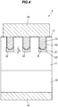
- FIG. 4 is a vertical cross-sectional view showing a trench MOS-type Schottky diode 2 in the second embodiment.
- the second semiconductor layer 11 of the trench MOS-type Schottky diode 2 has trenches 21 opened on the surface 17.
- An insulation 22 is embedded at the bottom of each trench 21 and the insulating film 15 covers the upper surface of the insulation 22 and the inner side surface of the trench 21.
- the trench MOS gate 16 is embedded in each trench 21 so as to be covered with the insulating film 15.
- an upper portion of the insulation 22 is roundly removed by etching to form the trench 12. Then, the insulating film 15 and the trench MOS gate 16 are formed in the trench 12.
- the bottom surface of the trench 21 may be flat or may be rounded in the same manner as the trench 12.
- the insulation 22 is formed of an insulating material with a lower permittivity than the insulating film 15. Therefore, when voltage is applied between the anode electrode 13 and the cathode electrode 14, an electric field applied to the insulation 22 is larger than that applied to the insulating film 15.
- the insulating film 15 has the highest electrical field strength in a region close to the bottom of the trench 12. Meanwhile, the second semiconductor layer 11 has the highest electrical field strength in a region immediately under the trench 12.
- the insulation 22 of the second embodiment it is possible to reduce the electrical field strength in a region of the insulating film 15 close to the bottom of the trench 12 and the electrical field strength in a region of the second semiconductor layer 11 immediately under the trench 12. In other words, it is possible to reduce the maximum electric field strength in the insulating film 15 and the maximum electric field strength in the second semiconductor layer 11.
- the insulation 22 is preferably formed of a material with a low permittivity such as SiO 2 (relative permittivity of about 4).
- a thickness T b of the insulation 22 immediately under the lowest portion of the insulating film 15 is preferably not less than about 200 nm.
- the third embodiment is different from the second embodiment in that the insulations 22 are in contact with the first semiconductor layer 10.
- the explanation of the same features as those in the second embodiment will be omitted or simplified.
- FIGS. 5A and 5B are vertical cross-sectional views showing a trench MOS-type Schottky diode 3 in the third embodiment.
- the thickness T b of the insulation 22 is larger in the trench MOS-type Schottky diode 3 than in the trench MOS-type Schottky diode 2 of the second embodiment.
- the thickness T e of the second semiconductor layer 11 can be reduced to the level at which the insulations 22 are in contact with the first semiconductor layer 10, and on-resistance can be thereby reduced.
- on-resistance of the trench MOS-type Schottky diode 3 can be reduced to lower than on-resistance of the trench MOS-type Schottky diode 2, hence, loss can be further reduced.
- the insulation 22 of the trench MOS-type Schottky diode 3 may be provided so that the bottom portion thereof is in contact with the upper surface of the first semiconductor layer 10 as shown in FIG. 5A or sinks into the first semiconductor layer 10 as shown in FIG. 5B .
- the height of the lowest portion of the insulation 22 may be the same as the height of the interface between the first semiconductor layer 10 and the second semiconductor layer 11, or may be lower than the height of the interface between the first semiconductor layer 10 and the second semiconductor layer 11.
- the first to third embodiments it is possible to provide a trench MOS-type Schottky diode having a high withstand voltage and low loss by using Ga 2 O 3 as semiconductor layers.
- the optimal values of various parameters of the structure of the trench MOS-type Schottky diode 1 in the first embodiment were derived by performing simulations. The simulations were performed to find a relation between each parameter and the maximum electric field strength in the second semiconductor layer 11/the maximum electric field strength in the insulating film 15/the maximum electric field strength in a region of the second semiconductor layer 11 immediately under the anode electrode 13 (in a region from the interface with the anode electrode 13 to the depth of 0.5 ⁇ m).
- P 1 denotes a point with the highest electrical field strength E in the second semiconductor layer
- P 2 denotes a point with the highest electrical field strength E in the insulating film 15, and denotes a point with the highest electrical field strength E in a region of the second semiconductor layer 11 immediately under the anode electrode 13.
- the electrical field strength E at the point P 1 is the maximum electric field strength in the second semiconductor layer 11
- the electrical field strength E at the point P 2 is the maximum electric field strength in the insulating film 15
- the electrical field strength E at the point is the maximum electric field strength in a region of the second semiconductor layer 11 immediately under the anode electrode 13.
- FIG. 6 schematically shows the positions of the points P 1 , P 2 and in the trench MOS-type Schottky diode 1 in the simulations performed in Example 1.
- Example 1 one of the structural parameters shown in Table 1 below was changed in each simulation.
- the parameters fixed in the respective simulations are shown in the graphs ( FIGS. 7 to 12 ) showing the respective simulation results.
- the parameters (W f , W m , W t , N d ', V b ) of which values were not changed in all simulations are not shown in the graphs of FIGS. 7 to 12 .
- FIGS. 7A and 7B show a relation between relative permittivity of the insulating film 15 and the electrical field strength E at the points P 1 , P 2 and P 3 .
- the relative permittivity 9.3 and 22 in FIGS. 7A and 7B respectively correspond to relative permittivity of Al2O 3 and that of HfO 2 .
- FIG. 7A shows that the maximum electric field strength in the insulating film 15 decreases as permittivity of the insulating film 15 increases.
- FIGS. 8A and 8B show a relation between the thickness T i of the insulating film 15 and the electrical field strength E at the points P 1 , P 2 and P 3 .
- FIG. 8A shows that the maximum electric field strength in the second semiconductor layer 11 decreases as the thickness T i of the insulating film 15 increases.
- the maximum electric field strength in the second semiconductor layer 11 can be reduced to less than 8 MV/cm when the thickness T i of the insulating film 15 is adjusted to not less than 300 nm.
- dielectric breakdown strength of the insulating film 15 as an insulation is very high, the electric field strength in the insulating film 15 does not reach the dielectric breakdown strength under the conditions of this simulation, and does not cause any problem even when increased.
- FIGS. 9A and 9B show a relation between the depth Dt of the trench 12 and the electrical field strength E at the points P 1 , P 2 and P 3 .
- the maximum electric field strength in the second semiconductor layer 11 and the maximum electric field strength in the insulating film 15 can be kept low when the depth D t of the trench 12 is not more than about 6 ⁇ m, preferably not more than 4 ⁇ m.
- FIG. 9B shows that the maximum electric field strength in a region of the second semiconductor layer 11 immediately under the anode electrode 13 can be kept low when the depth D t of the trench 12 is not less than about 2 ⁇ m, preferably not less than 3 ⁇ m.
- FIGS. 10A and 10B show a relation between the thickness T e of the second semiconductor layer 11 and the electrical field strength E at the points P 1 , P 2 and P 3 .
- the maximum electric field strength in the second semiconductor layer 11 can be reduced to less than 8 MV/cm, which is dielectric breakdown strength of Ga 2 O 3 , when the thickness T e of the second semiconductor layer 11 is adjusted to about not less than 5.5 ⁇ m.
- FIGS. 11A and 11B show a relation between the donor concentration N d in the second semiconductor layer 11 and the electrical field strength E at the points P 1 , P 2 and P 3 .
- the maximum electric field strength in the second semiconductor layer 11 can be reduced to less than 8 MV/cm, which is dielectric breakdown strength of Ga 2 O 3 , when the donor concentration N d in the second semiconductor layer 11 is adjusted to about not more than 6.0x10 16 cm -3 .
- FIGS. 12A and 12B show a relation between the 1/2 width W m of the mesa-shaped portion between adjacent trenches 12 and the electrical field strength E at the points P 1 , P 2 and P 3 .
- FIGS. 12A and 12B show that the width of the mesa-shaped portion has a large impact particularly on the maximum electric field strength in a region of the second semiconductor layer 11 immediately under the anode electrode 13. Based on FIG. 12B , the maximum electric field strength in a region of the second semiconductor layer 11 immediately under the anode electrode 13 decreases as the width of the mesa-shaped portion decreases.
- FIG. 13 shows a relation between the electrical field strength E at the points P 1 , P 2 , and the barrier height at an interface between the anode electrode 13 and the second semiconductor layer 11.
- FIG. 13 shows that the maximum electric field strength in a region of the second semiconductor layer 11 immediately under the anode electrode 13, the maximum electric field strength in the second semiconductor layer 11 and the maximum electric field strength in the insulating film 15 do not depend on the barrier height at the interface between the anode electrode 13 and the second semiconductor layer 11.
- withstand voltage increases with increase in the thickness T e of the second semiconductor layer 11 and the thickness T e of the second semiconductor layer 11 is preferably not more than about 9 ⁇ m in view of downsizing of the trench MOS-type Schottky diode 1, the donor concentration N d of about not less than 3.0 ⁇ 10 16 cm -3 and not more than 6.0 ⁇ 10 16 cm -3 and the thickness T e of the second semiconductor layer 11 of about not less than 5.5 ⁇ m and not more than 9 ⁇ m are preferable to form an element with a withstand voltage of 1200V.
- the thickness T e of the second semiconductor layer 11 can be further reduced.
- the donor concentration N d is about not less than 3.0 ⁇ 10 16 cm -3 and not more than 6.0 ⁇ 10 16 cm -3 and the thickness T e of the second semiconductor layer 11 is about not less than 4.5 ⁇ m and not more than 9 ⁇ m.
- Table 2 shows examples of structural parameters of the trench MOS-type Schottky diode 1 with a withstand voltage of 1200V which were derived based on the simulation results described above.
- Table 2 1/2 width W m of mesa-shaped portion 0.5 ⁇ m 1/2 width W t of trench 12 1 ⁇ m Thickness T i of insulating film 15 50 nm Thickness T e of second semiconductor layer 11 7 ⁇ m Depth D t of trench 12 3 ⁇ m Relative permittivity ⁇ s of insulating film 15 22 (HfO 2 ) Donor concentration N d ' of first semiconductor layer 10 Not less than 1.0x10 19 cm -3 Thickness T s of first semiconductor layer 10 Not more than 100 ⁇ m Donor concentration N d of second semiconductor layer 11 3.0x10 16 cm -3
- On-resistance of the second semiconductor layer 11 and that of the first semiconductor layer 10 were respectively 1.6 m ⁇ cm 2 and 0.05 m ⁇ cm 2 .
- On-resistance of the second semiconductor layer 11 not having a trench structure, when calculated from resistivity of the second semiconductor layer 11, is 1.3 m ⁇ cm 2
- 1.6 m ⁇ cm 2 is the value derived on the assumption that the loss rises 1.2-fold due to the trench structure.
- FIG. 14 shows a relation between reverse leakage current and the barrier height at the interface between the anode electrode 13 and the second semiconductor layer 11.
- the relation between the barrier height and the reverse leakage current shown in FIG. 14 was obtained from theoretical calculation, taking into account thermionic emission as well as mirror effect and on the assumption that the electrical field strength immediately under the anode electrode is 0.4 MV/cm.
- the minimum value of the allowable barrier height is 0.7 eV when the upper limit of the allowable leakage current is 1 ⁇ A (1x10 16 A).
- FIG. 15 shows forward characteristics of the trench MOS-type Schottky diode 1 with a withstand voltage of 1200V when calculated using on-resistance and barrier height described above. Based on FIG. 15 , forward voltage when driving at, e.g., 200 A/cm 2 is 0.7 to 0.8V.
- Table 3 shows examples of structural parameters of the trench MOS-type Schottky diode 1 with a withstand voltage of 600V which were derived in the same manner based on the simulation results described above.
- Table 3 1/2 width W m of mesa-shaped portion 0.5 ⁇ m 1/2 width W t of trench 12 1 ⁇ m Thickness T i of insulating film 15 50 nm Thickness T e of second semiconductor layer 11 4.5 ⁇ m Depth D t of trench 12 3 ⁇ m Relative permittivity ⁇ s of insulating film 15 22 (HfO 2 ) Donor concentration N d ' of first semiconductor layer 10 Not less than 1.0x10 19 cm -3 Thickness T s of first semiconductor layer 10 Not more than 100 ⁇ m Donor concentration N d of second semiconductor layer 11 3.0x10 16 cm -3
- On-resistance of the second semiconductor layer 11 and that of the first semiconductor layer 10 were respectively 1.0 m ⁇ cm 2 and 0.05 m ⁇ cm 2 .
- On-resistance of the second semiconductor layer 11 not having a trench structure, when calculated from resistivity of the second semiconductor layer 11, is 0.86 m ⁇ cm 2
- 1.0 m ⁇ cm 2 is the value derived on the assumption that the loss rises 1.2-fold due to the trench structure.
- FIG. 16 shows a relation between reverse leakage current and the barrier height at the interface between the anode electrode 13 and the second semiconductor layer 11.
- the relation between the barrier height and the reverse leakage current shown in FIG. 16 was obtained from theoretical calculation, taking into account thermionic emission as well as mirror effect and on the assumption that the electrical field strength immediately under the anode electrode is 0.2 MV/cm.
- the minimum value of the allowable barrier height is 0.7 eV when the upper limit of the allowable leakage current is 1 ⁇ A (1x10 16 A).
- FIG. 17 shows forward characteristics of the trench MOS-type Schottky diode 1 with a withstand voltage of 600V when calculated using on-resistance and barrier height described above. Based on FIG. 17 , forward voltage when driving at, e.g., 200 A/cm 2 is 0.6 to 0.7V.
- Example 1 Although only the calculation results when withstand voltage is 1200V and 600V are shown in Example 1, elements having different withstand voltages can be also easily designed based on the calculation results in Example 1. For example, when designing an element with a withstand voltage 300V, the value of the electrical field strength in each part calculated to have withstand voltage of 1200V is reduced to a quarter, and structural parameters are changed accordingly.
- the donor concentration N d of about not less than 3.0x10 16 cm -3 and not more than 3.0x10 17 cm -3 and the thickness T e of about not less than 2.0 ⁇ m and not more than 4.5 ⁇ m.
- the donor concentration N d of about not less than 1.0x10 16 cm -3 and not more than 3.0x10 16 cm -3 and the thickness T e of about not less than 5.5 ⁇ m and not more than 9 ⁇ m.
- the donor concentration N d of about not less than 1.0x10 15 cm -3 and not more than 1.0x10 16 cm -3 and the thickness T e of about not less than 9 ⁇ m and not more than 50 ⁇ m.
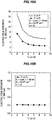
- FIGS. 18A, 18B and 18C show a relation between the thickness T b of the insulation 22 immediately under the lowest portion of the film 15 and the electrical field strength E at the points P 1 , P 2 , and P 4 .
- the point P 4 here is a point with the highest electrical field strength E in the insulation 22.
- the point P 1 with the highest electrical field strength E in the second semiconductor layer 11 is located in the vicinity of a side surface of the insulation 22.
- FIGS. 18A, 18B and 18C show that the maximum electric field strength in the second semiconductor layer 11, the maximum electric field strength in the insulating film 15 and the maximum electric field strength in the insulation 22 decrease as the thickness T b of the insulation 22 increases. Meanwhile, even when the thickness T b of the insulation 22 increases, the maximum electric field strength in a region of the second semiconductor layer 11 immediately under the anode electrode 13 hardly changes.
- the maximum electric field strength in a region of the second semiconductor layer 11 immediately under the anode electrode 13 increases as shown in FIG. 8B .
- the maximum electric field strength in the second semiconductor layer 11 is kept low by adjusting the thickness T b of the insulation 22 to about not less than 200 nm.
- a trench MOS-type Schottky diode having a high withstand voltage and low loss.
Landscapes
- Electrodes Of Semiconductors (AREA)
Abstract
Description
- The invention relates to a trench MOS-type Schottky diode.
- Schottky barrier diode (Schottky diode) using Ga2O3 as a semiconductor layer is known (e.g., PTL 1).
- In
PTL 1, it is described that when an n-Ga2O3 layer has, e.g., an electron carrier concentration of 9.95x1016 cm-3 and a thickness of 3.3 µm, withstand voltage of the Schottky diode is 1000V. - Trench MOS-type Schottky diode using Si as a semiconductor layer and trench MOS-type Schottky diode using SiC as a semiconductor layer are also known (e.g.,
NPLs 1 and 2). - In
NPL 1, it is described that when an n-Si layer has a doping concentration of 1x1016 cm-3 and a thickness of 9 µm, withstand voltage of the trench MOS-type Schottky diode using Si as a semiconductor layer is 107V. - Based on the reverse voltage/reverse current characteristic described in
NPL 2, withstand voltage of the trench MOS-type Schottky diode using SiC as a semiconductor layer is about several tens of V when an n-SiC layer has a doping concentration of 6x1015 cm-3 and a thickness of 4 µm. - PTL 1:
JP 2013/102081 A -
- NPL 1: T. Shimizu et al., Proceedings of 2001 International Symposium on Power Semiconductor Devices & ICs, Osaka, pp.243-246 (2001)
- NPL 2: V. Khemka, et al., IEEE ELECTRON DEVICE LETTERS, VOL.21, NO.5, MAY 2000, pp.286-288
- In
PTL 1, withstand voltage of the Schottky diode is defined by breakdown field strength of Ga2O3. However, when reverse voltage is increased in a Schottky diode using a material with high breakdown field strength such as Ga2O3, a leakage current between an anode electrode and a Ga2O3 layer increases drastically before breakdown of the Ga2O3 layer occurs, and the Schottky diode burns out. - Thus, it is appropriate that reverse voltage when a leakage current of a predetermined magnitude (e.g., 1 µA) flows is defined as withstand voltage for a Schottky diode using Ga2O3 as a semiconductor layer. Note that, the Schottky diode described in
PTL 1 does not have a special structure to reduce a leakage current and the roughly estimated reverse voltage at a leakage current of 1 µA is about 64V when the n-Ga2O3 layer has a carrier concentration of 9.95x1016 cm-3. - It is an object of the invention to provide a trench MOS-type Schottky diode having a high withstand voltage and low loss.
- To achieve the above-mentioned object, an aspect of the invention provides a trench MOS-type Schottky diode defined by [1] to [7] below.
- [1] A trench MOS-type Schottky diode, comprising: a first semiconductor layer comprising a Ga2O3-based single crystal; a second semiconductor layer that is a layer laminated on the first semiconductor layer, and that comprises a Ga2O3-based single crystal and a trench opened on a surface thereof opposite to the first semiconductor layer, an anode electrode formed on the surface of the second semiconductor layer opposite to the first semiconductor layer; a cathode electrode formed on a surface of the first semiconductor layer opposite to the second semiconductor layer; an insulating film covering the inner surface of the trench of the second semiconductor layer; and a trench MOS gate that is embedded in the trench of the second semiconductor layer so as to be covered with the insulating film and is in contact with the anode electrode.
- [2] The trench MOS-type Schottky diode defined by [1], wherein a donor concentration in the second semiconductor layer is not less than 1.0x1015 cm-3 and not more than 3.0x1017 cm-3, and a thickness of the second semiconductor layer is not less than 2.0 µm and not more than 50 µm.
- [3] The trench MOS-type Schottky diode defined by [2], wherein the donor concentration in the second semiconductor layer is not less than 3.0x1016 cm-3 and not more than 6.0x1016 cm-3, and the thickness of the second semiconductor layer is not less than 4.5 µm and not more than 9 µm.
- [4] The trench MOS-type Schottky diode defined by [3], wherein the thickness of the second semiconductor layer is not less than 5.5 µm.
- [5] The trench MOS-type Schottky diode defined by any one of [1] to [4], wherein a lower surface of the insulating film is covered with an insulation having a lower permittivity than the insulating film.
- [6] The trench MOS-type Schottky diode defined by [5], wherein a thickness of the insulation immediately under the lowest portion of the insulating film is not less than 200 nm.
- [7] The trench MOS-type Schottky diode defined by [5], wherein the insulation is in contact with the first semiconductor layer.
- According to the invention, it is possible to provide a trench MOS-type Schottky diode having a high withstand voltage and low loss.
-
-
FIG. 1 is a vertical cross-sectional view showing a trench MOS-type Schottky diode in the first embodiment. -
FIG. 2A is a top view showing a typical example of a planar trench pattern on a second semiconductor layer. -
FIG. 2B is a top view showing another typical example of a planar trench pattern on the second semiconductor layer. -
FIG. 3 is a vertical cross-sectional view showing a modification of the trench MOS-type Schottky diode in the first embodiment. -
FIG. 4 is a vertical cross-sectional view showing a trench MOS-type Schottky diode in the second embodiment. -
FIG. 5A is a vertical cross-sectional view showing a trench MOS-type Schottky diode in the third embodiment. -
FIG. 5B is a vertical cross-sectional view showing a trench MOS-type Schottky diode in the third embodiment. -
FIG. 6 schematically shows the positions of points P1, P2 and P3 in the trench MOS-type Schottky diode in the simulations performed in Example. -
FIG. 7A shows a relation between relative permittivity of an insulating film and electrical field strength E at the points P1 and P2. -
FIG. 7B shows a relation between relative permittivity of the insulating film and electrical field strength E at the point P3. -
FIG. 8A shows a relation between thickness Ti of the insulating film and electrical field strength E at the points P1 and P2. -
FIG. 8B shows a relation between thickness Ti of the insulating film and electrical field strength E at the point P3. -
FIG. 9A shows a relation between depth Dt of a trench and electrical field strength E at the points P1 and P2. -
FIG. 9B shows a relation between depth Dt of the trench and electrical field strength E at the point P3. -
FIG. 10A shows a relation between thickness Te of the second semiconductor layer and electrical field strength E at the points P1 and P2. -
FIG. 10B shows a relation between thickness Te of the second semiconductor layer and electrical field strength E at the point P3. -
FIG. 11A shows a relation between donor concentration Nd in the second semiconductor layer and electrical field strength E at the points P1 and P2. -
FIG. 11B shows a relation between donor concentration Nd in the second semiconductor layer and electrical field strength E at the point P3. -
FIG. 12A shows a relation between 1/2 width Wm of a mesa-shaped portion between adjacent trenches and electrical field strength E at the points P1 and P2. -
FIG. 12B shows a relation between 1/2 width Wm of the mesa-shaped portion between adjacent trenches and electrical field strength E at the point P3. -
FIG. 13 shows a relation between electrical field strength E at the points P1, P2, and barrier height at an interface between an anode electrode and the second semiconductor layer. -
FIG. 14 shows a relation between reverse leakage current and barrier height at the interface between the anode electrode and the second semiconductor layer. -
FIG. 15 shows forward characteristics of the trench MOS-type Schottky diode with a withstand voltage of 1200V when calculated using on-resistance and barrier height derived by simulation. -
FIG. 16 shows a relation between reverse leakage current and barrier height at the interface between the anode electrode and the second semiconductor layer. -
FIG. 17 shows forward characteristics of the trench MOS-type Schottky diode with a withstand voltage of 600V when calculated using on-resistance and barrier height derived by simulation. -
FIG. 18A shows a relation between thickness Tb of an insulation immediately under the lowest portion of the insulating film and electrical field strength E at the points P1 and P2. -
FIG. 18B shows a relation between thickness Tb of the insulation immediately under the lowest portion of the insulating film and electrical field strength E at the point P3. -
FIG. 18C shows a relation between thickness Tb of the insulation immediately under the lowest portion of the insulating film and electrical field strength E at the point P4. -
FIG. 1 is a vertical cross-sectional view showing a trench MOS-type Schottky diode 1 in the first embodiment. The trench MOS-type Schottky diode 1 is a vertical Schottky diode having a trench MOS region. - The trench MOS-
type Schottky diode 1 has afirst semiconductor layer 10, asecond semiconductor layer 11 which is a layer laminated on thefirst semiconductor layer 10 and hastrenches 12 opened on asurface 17 thereof opposite to thefirst semiconductor layer 10, ananode electrode 13 formed on thesurface 17 of thesecond semiconductor layer 11, acathode electrode 14 formed on a surface of thefirst semiconductor layer 10 opposite to thesecond semiconductor layer 11, insulatingfilms 15 covering inner surfaces of thetrenches 12 of thesecond semiconductor layer 11, and trenchMOS gates 16 which are embedded in thetrenches 12 of thesecond semiconductor layer 11 so as to be covered with the insulatingfilms 15 and are in contact with theanode electrode 13. - In the trench MOS-
type Schottky diode 1, an energy barrier at an interface between theanode electrode 13 and thesecond semiconductor layer 11 as viewed from thesecond semiconductor layer 11 is lowered by applying forward voltage between theanode electrode 13 and the cathode electrode 14 (positive potential on theanode electrode 13 side), allowing an electric current to flow from theanode electrode 13 to thecathode electrode 14. - On the other hand, when reverse voltage is applied between the
anode electrode 13 and the cathode electrode 14 (negative potential on theanode electrode 13 side), the electric current does not flow due to the Schottky barrier. When reverse voltage is applied between theanode electrode 13 and thecathode electrode 14, a depletion layer spreads from an interface between theanode electrode 13 and thesecond semiconductor layer 11 and from an interface between the insulatingfilms 15 and thesecond semiconductor layer 11. - In general, the upper limit of reverse leakage current in Schottky diode is set to 1 µA. In the embodiments, reverse voltage when a leakage current of 1 µA flows is defined as withstand voltage.
- According to data of dependence of reverse leakage current on electric field strength at Schottky interface in Schottky diode having a SiC semiconductor layer described in, e.g., "Technology of Semiconductor SiC and its Application" by Hiroyuki Matsunami, Noboru Otani, Tsunenobu Kimoto und Takashi Nakamura, Second Edition, Nikkan Kogyo Shimbun, Ltd., September 30, 2011, p.355, electric field strength immediately under Schottky electrode is about 0.8 MV/cm when a current density of reverse leakage current is 0.0001 A/cm2. 0.0001 A/cm2 here is a current density immediately under the Schottky electrode when an electric current of 1 µA flows through the Schottky electrode having a size of 1 mm × 1 mm.
- Thus, even when breakdown field strength of the semiconductor material itself is several MV/cm, a leakage current of more than 1 µA flows when the electric field strength immediately under the Schottky electrode exceeds 0.8 MV/cm.
- In order to obtain withstand voltage of 1200V in, e.g., a conventional Schottky diode not having a special structure to reduce electric field strength immediately under Schottky electrode, a donor concentration in a semiconductor layer needs to be reduced to the order of 1015 cm-3 and also the semiconductor layer needs to be very thick so that the electric field strength immediately under the Schottky electrode is kept not more than 0.8 MV/cm. This causes a significant increase in conduction loss, and it is thus difficult to make a Schottky barrier diode having a high withstand voltage and low loss.
- The trench MOS-
type Schottky diode 1 in the first embodiment has a trench MOS structure and thus can have a high withstand voltage without an increase in resistance of the semiconductor layer. In other words, the trench MOS-type Schottky diode 1 is a Schottky diode having a high withstand voltage and low loss. - Junction barrier Schottky (JBS) diode is known as a Schottky diode having a high withstand voltage and low loss. However, Ga2O3 is not suitable as a material for the JBS diode requiring a p-type region since it is difficult to manufacture p-type Ga2O3.
- The
first semiconductor layer 10 is formed of an n-type Ga2O3-based single crystal containing a Group IV element, such as Si or Sn, as a donor. A donor concentration Nd' of thefirst semiconductor layer 10 is, e.g., not less than 1.0x10¹⁸ and not more than 1.0x1020 cm-3. A thickness Ts of thefirst semiconductor layer 10 is, e.g., 10 to 600 µm. Thefirst semiconductor layer 10 is, e.g., a Ga2O3-based single crystal substrate. - The Ga2O3-based single crystal here means a Ga2O3 single crystal or is a Ga2O3 single crystal doped with an element such as Al or In, and may be, e.g., a (GaxAlyIn(1-x-y))2O3 (0<x≤1, 0≤y<1, 0<x+y≤1) single crystal which is a Ga2O3 single crystal doped with Al and In. The band gap is widened by adding Al and is narrowed by adding In. The Ga2O3 single crystal mentioned above has, e.g., a β-crystal structure.
- The
second semiconductor layer 11 is formed of an n-type Ga2O3-based single crystal containing a Group IV element, such as Si or Sn, as a donor. A donor concentration Nd of thesecond semiconductor layer 11 is lower than the donor concentration Nd of thefirst semiconductor layer 10. Thesecond semiconductor layer 11 is, e.g., an epitaxial layer epitaxially grown on thefirst semiconductor layer 10 which is a Ga2O3-based single crystal substrate. - A high-donor-concentration layer containing a high concentration of donor may be additionally formed between the
first semiconductor layer 10 and thesecond semiconductor layer 11. The high-donor-concentration layer is used when, e.g., thesecond semiconductor layer 11 is epitaxially grown on thefirst semiconductor layer 10 as a substrate. At the early growth stage of thesecond semiconductor layer 11, the amount of dopant incorporated thereinto is unstable and an acceptor impurity is diffused from thefirst semiconductor layer 10 as a substrate. Thus, resistance increases in a region of thesecond semiconductor layer 11 close to the interface with thefirst semiconductor layer 10 when thesecond semiconductor layer 11 is grown directly on thefirst semiconductor layer 10. The high-donor-concentration layer is used to avoid such problems. The concentration in the high-donor-concentration layer is set to be, e.g., higher than the concentration in thesecond semiconductor layer 11, more preferably, higher than the concentration in thefirst semiconductor layer 10. - As the donor concentration Nd in the
second semiconductor layer 11 increases, electrical field strength in each part of the trench MOS-type Schottky diode 1 increases. The donor concentration Nd in thesecond semiconductor layer 11 is preferably not more than about 6.0x1016 cm-3 to lower the maximum electric field strength in a region of thesecond semiconductor layer 11 immediately under theanode electrode 13, the maximum electric field strength in thesecond semiconductor layer 11 and the maximum electric field strength in the insulatingfilm 15. On the other hand, as the donor concentration Nd decreases, resistance of thesecond semiconductor layer 11 increases and the forward loss increases. Therefore, to obtain withstand voltage of, e.g., not more than 1200V, the donor concentration Nd is preferably not less than 3.0x1016 cm-3. However, to obtain higher withstand voltage, the donor concentration Nd is preferably reduced to, e.g., about 1.0x1016 cm-3. - As a thickness Te of the
second semiconductor layer 11 increases, the maximum electric field strength in thesecond semiconductor layer 11 and the maximum electric field strength in the insulatingfilm 15 decrease. By adjusting the thickness Te of thesecond semiconductor layer 11 to not less than about 6 µm, it is possible to effectively reduce the maximum electric field strength in thesecond semiconductor layer 11 and the maximum electric field strength in the insulatingfilm 15. In view of reduction in these maximum electric field strengths and downsizing of the trench MOS-type Schottky diode 1, the thickness Te of thesecond semiconductor layer 11 is preferably about not less than 5.5 µm and not more than 9 µm. - Electrical field strength in each part of the trench MOS-
type Schottky diode 1 changes depending on a depth Dt of thetrench 12. The depth Dt of thetrench 12 is preferably about not less than 2 µm and not more than 6 µm, more preferably, about not less than 3 µm and not more than 4 µm to lower the maximum electric field strength in a region of thesecond semiconductor layer 11 immediately under theanode electrode 13, the maximum electric field strength in thesecond semiconductor layer 11 and the maximum electric field strength in the insulatingfilm 15. In the present specification, half of the width of the trench 12 (hereinafter, referred to as "1/2 width") is denoted as Wt. - As a width of a mesa-shaped portion between
adjacent trenches 12 on thesecond semiconductor layer 11 decreases, the maximum electric field strength in a region of thesecond semiconductor layer 11 immediately under theanode electrode 13 decreases. In the present specification, half of the width of the mesa-shaped portion between adjacent trenches 12 (hereinafter, referred to as "1/2 width") is denoted as Wm. The 1/2 width Wm of the mesa-shaped portion is preferably not more than 1.25 µm to lower the maximum electric field strength in a region of thesecond semiconductor layer 11 immediately under theanode electrode 13. At the same time, the 1/2 width Wm of the mesa-shaped portion is preferably not less than 0.25 µm since it is more difficult to make thetrench 12 when the width of the mesa-shaped portion is smaller. - Since the maximum electric field strength in the insulating
film 15 decreases as permittivity of the insulatingfilm 15 increases, the insulatingfilm 15 is preferably formed of a high-permittivity material. For example, Al2O3 (relative permittivity of about 9.3) and HfO2 (relative permittivity of about 22) can be used as a material of the insulatingfilm 15, and it is particularly preferable to use HfO2 which has high permittivity. - Meanwhile, as a thickness Ti of the insulating
film 15 increases, the maximum electric field strength in thesecond semiconductor layer 11 decreases but the maximum electric field strength in the insulatingfilm 15 and the maximum electric field strength in a region of thesecond semiconductor layer 11 immediately under theanode electrode 13 increase. In view of ease of manufacturing, the thickness of the insulatingfilm 15 is preferably smaller, and is more preferably not more than 300 nm. It is, however, obvious that a certain thickness is required so that an electric current virtually does not flow directly between thetrench MOS gate 16 and thesecond semiconductor layer 11. - The material of the
trench MOS gate 16 is not specifically limited as long as it is electrically conductive, and it is possible to use, e.g., polycrystalline Si doped at a high concentration and a metal such as Ni or Au. - Electric field strength in the trench MOS-
type Schottky diode 1 is affected by the width of the mesa-shaped portion between twoadjacent trenches 12, the depth Dt of thetrench 12 and the thickness Ti of the insulatingfilm 15, etc., as described above, but is hardly affected by a planar pattern of thetrenches 12. Thus, the planar pattern of thetrenches 12 on thesecond semiconductor layer 11 is not specifically limited. -
FIGS. 2A and 2B are top views respectively showing typical examples of the planar pattern of thetrenches 12 on thesurface 17 of thesecond semiconductor layer 11. - The
trenches 12 shown inFIG. 2A are formed in a line-shaped planar pattern. Thetrenches 12 shown inFIG. 2B are formed in a planar pattern with dots each of which is the mesa-shaped portion between twoadjacent trenches 12. - The cross section of the trench MOS-
type Schottky diode 1 shown inFIG. 1 corresponds to a cross section cut along line A-A in case of the trench MOS-type Schottky diode 1 shown inFIG. 2A and a cross section cut along line B-B in case of the trench MOS-type Schottky diode 1 shown inFIG. 2B . - The
anode electrode 13 is in Schottky contact with thesecond semiconductor layer 11. Theanode electrode 13 is formed of Pt, Pd, Au, Ni, Ag, Cu, Al, Mo, In, Ti or polycrystalline Si, or oxide, nitride or alloy thereof, etc. A reverse leakage current at an interface between theanode electrode 13 and thesecond semiconductor layer 11 is smaller when a height of a barrier (barrier height) at the interface between theanode electrode 13 and thesecond semiconductor layer 11 is higher. Meanwhile, when a metal with a high barrier height is used to form theanode electrode 13, forward rising voltage increases and the forward loss thus increases. Therefore, it is preferable to select a material having a barrier height so that the reverse leakage current is about 1 µA at a maximum. When reverse withstand voltage is, e.g., 600V to 1200V, it is possible to maximize reduction of forward loss by adjusting the barrier height to about 0.7 eV while keeping the reverse leakage current down to about 1 µA. Theanode electrode 13 may have a multilayer structure formed by laminating different metal films, e.g., Pt/Au, Pt/Al, Pd/Au, Pd/Al, Pt/Ti/Au or Pt/Ti/Au. - The
cathode electrode 14 is in ohmic contact with thefirst semiconductor layer 10. Thecathode electrode 14 is formed of a metal such as Ti. Thecathode electrode 14 may have a multilayer structure formed by laminating different metal films, e.g., Ti/Au or Ti/Al. For reliable ohmic contact between thecathode electrode 14 and thefirst semiconductor layer 10, thecathode electrode 14 is preferably configured that a layer in contact with thefirst semiconductor layer 10 is formed of Ti. -
FIG. 3 is a vertical cross-sectional view showing a modification of the trench MOS-type Schottky diode 1 in the first embodiment. The trench MOS-type Schottky diode 1 may have a field-plate structure as shown inFIG. 3 . - In the modification shown in
FIG. 3 , adielectric film 18 formed of SiO2, etc., is provided along an edge of thesurface 17 of thesecond semiconductor layer 11 and theanode electrode 13 is arranged so that an edge thereof rides on thedielectric film 18. - By providing such field-plate structure, it is possible to prevent the electric field from concentrating at an edge portion of the
anode electrode 13. Thedielectric film 18 also serves as a passivation film for preventing a surface leakage current which flows along thesurface 17 of thesecond semiconductor layer 11. Having or not having the field-plate structure does not affect the optimal values of various parameters (the 1/2 width Wm of the mesa-shaped portion, the depth Dt of thetrench 12, the thickness Ti of the insulatingfilm 15, etc.) of the structure of the trench MOS-type Schottky diode 1. - The second embodiment is different from the first embodiment in that an insulation different from the insulation constituting the insulating
film 15 is embedded at the bottom of each trench. The explanation of the same features as those in the first embodiment will be omitted or simplified. -
FIG. 4 is a vertical cross-sectional view showing a trench MOS-type Schottky diode 2 in the second embodiment. - The
second semiconductor layer 11 of the trench MOS-type Schottky diode 2 hastrenches 21 opened on thesurface 17. Aninsulation 22 is embedded at the bottom of eachtrench 21 and the insulatingfilm 15 covers the upper surface of theinsulation 22 and the inner side surface of thetrench 21. Thetrench MOS gate 16 is embedded in eachtrench 21 so as to be covered with the insulatingfilm 15. - For example, after embedding the
insulation 22 at the bottom of thetrench 21, an upper portion of theinsulation 22 is roundly removed by etching to form thetrench 12. Then, the insulatingfilm 15 and thetrench MOS gate 16 are formed in thetrench 12. The bottom surface of thetrench 21 may be flat or may be rounded in the same manner as thetrench 12. - The
insulation 22 is formed of an insulating material with a lower permittivity than the insulatingfilm 15. Therefore, when voltage is applied between theanode electrode 13 and thecathode electrode 14, an electric field applied to theinsulation 22 is larger than that applied to the insulatingfilm 15. - In the trench MOS-
type Schottky diode 1 of the first embodiment, the insulatingfilm 15 has the highest electrical field strength in a region close to the bottom of thetrench 12. Meanwhile, thesecond semiconductor layer 11 has the highest electrical field strength in a region immediately under thetrench 12. - By providing the
insulation 22 of the second embodiment, it is possible to reduce the electrical field strength in a region of the insulatingfilm 15 close to the bottom of thetrench 12 and the electrical field strength in a region of thesecond semiconductor layer 11 immediately under thetrench 12. In other words, it is possible to reduce the maximum electric field strength in the insulatingfilm 15 and the maximum electric field strength in thesecond semiconductor layer 11. - The
insulation 22 is preferably formed of a material with a low permittivity such as SiO2 (relative permittivity of about 4). A thickness Tb of theinsulation 22 immediately under the lowest portion of the insulatingfilm 15 is preferably not less than about 200 nm. Theinsulation 22 has the same planar pattern as thetrench 12 and typically has a width substantially equal to the width of the trench 12 (=2Wt). - The third embodiment is different from the second embodiment in that the
insulations 22 are in contact with thefirst semiconductor layer 10. The explanation of the same features as those in the second embodiment will be omitted or simplified. -
FIGS. 5A and 5B are vertical cross-sectional views showing a trench MOS-type Schottky diode 3 in the third embodiment. - The thickness Tb of the
insulation 22 is larger in the trench MOS-type Schottky diode 3 than in the trench MOS-type Schottky diode 2 of the second embodiment. Thus, it is possible to provide sufficient withstand voltage only by theinsulations 22, unlike the trench MOS-type Schottky diode 2 which uses theinsulations 22 and thesecond semiconductor layer 11 to provide sufficient withstand voltage. - Thus, the thickness Te of the
second semiconductor layer 11 can be reduced to the level at which theinsulations 22 are in contact with thefirst semiconductor layer 10, and on-resistance can be thereby reduced. In other words, when the trench MOS-type Schottky diode 2 and the trench MOS-type Schottky diode 3 are designed to have the same withstand voltage, on-resistance of the trench MOS-type Schottky diode 3 can be reduced to lower than on-resistance of the trench MOS-type Schottky diode 2, hence, loss can be further reduced. - The
insulation 22 of the trench MOS-type Schottky diode 3 may be provided so that the bottom portion thereof is in contact with the upper surface of thefirst semiconductor layer 10 as shown inFIG. 5A or sinks into thefirst semiconductor layer 10 as shown inFIG. 5B . In other words, the height of the lowest portion of theinsulation 22 may be the same as the height of the interface between thefirst semiconductor layer 10 and thesecond semiconductor layer 11, or may be lower than the height of the interface between thefirst semiconductor layer 10 and thesecond semiconductor layer 11. - According to the first to third embodiments, it is possible to provide a trench MOS-type Schottky diode having a high withstand voltage and low loss by using Ga2O3 as semiconductor layers.
- The optimal values of various parameters of the structure of the trench MOS-
type Schottky diode 1 in the first embodiment were derived by performing simulations. The simulations were performed to find a relation between each parameter and the maximum electric field strength in thesecond semiconductor layer 11/the maximum electric field strength in the insulatingfilm 15/the maximum electric field strength in a region of thesecond semiconductor layer 11 immediately under the anode electrode 13 (in a region from the interface with theanode electrode 13 to the depth of 0.5 µm). - Here, P1 denotes a point with the highest electrical field strength E in the
second semiconductor layer 11, P2 denotes a point with the highest electrical field strength E in the insulatingfilm 15, and denotes a point with the highest electrical field strength E in a region of thesecond semiconductor layer 11 immediately under theanode electrode 13. In other words, the electrical field strength E at the point P1 is the maximum electric field strength in thesecond semiconductor layer 11, the electrical field strength E at the point P2 is the maximum electric field strength in the insulatingfilm 15, and the electrical field strength E at the point is the maximum electric field strength in a region of thesecond semiconductor layer 11 immediately under theanode electrode 13. -
FIG. 6 schematically shows the positions of the points P1, P2 and in the trench MOS-type Schottky diode 1 in the simulations performed in Example 1. - In Example 1, one of the structural parameters shown in Table 1 below was changed in each simulation. The parameters fixed in the respective simulations are shown in the graphs (
FIGS. 7 to 12 ) showing the respective simulation results. The parameters (Wf, Wm, Wt, Nd', Vb) of which values were not changed in all simulations are not shown in the graphs ofFIGS. 7 to 12 .Table 1 Work function Wf of anode electrode 135.32 eV 1/2 width Wm of mesa-shaped portion 0.5 µm 1/2 width Wt of trench 121.0 µm Thickness Ti of insulating film 1520 - 500 nm Thickness Te of second semiconductor layer 114 - 9 µm Depth Dt of trench 121-7 µm Relative permittivity εs of insulating film 159.3 or 22 Donor concentration Nd' of first semiconductor layer 101.0x1019 cm-3 Donor concentration Nd of second semiconductor layer 113.0x10¹⁶ - 8.0x1016 cm-3 Applied voltage Vb 1200V -
FIGS. 7A and 7B show a relation between relative permittivity of the insulatingfilm 15 and the electrical field strength E at the points P1, P2 and P3. The relative permittivity 9.3 and 22 inFIGS. 7A and 7B respectively correspond to relative permittivity of Al2O3 and that of HfO2. -
FIG. 7A shows that the maximum electric field strength in the insulatingfilm 15 decreases as permittivity of the insulatingfilm 15 increases. -
FIGS. 8A and 8B show a relation between the thickness Ti of the insulatingfilm 15 and the electrical field strength E at the points P1, P2 and P3. -
FIG. 8A shows that the maximum electric field strength in thesecond semiconductor layer 11 decreases as the thickness Ti of the insulatingfilm 15 increases. - In a literature, "M. Higashiwaki et al., Appl. Phys. Lett. 100, 013504 (2012)", it is reported that dielectric breakdown strength of Ga2O3 is about 8 MV/cm. Based on
FIG. 8A , the maximum electric field strength in thesecond semiconductor layer 11 can be reduced to less than 8 MV/cm when the thickness Ti of the insulatingfilm 15 is adjusted to not less than 300 nm. - Since dielectric breakdown strength of the insulating
film 15 as an insulation is very high, the electric field strength in the insulatingfilm 15 does not reach the dielectric breakdown strength under the conditions of this simulation, and does not cause any problem even when increased. -
FIGS. 9A and 9B show a relation between the depth Dt of thetrench 12 and the electrical field strength E at the points P1, P2 and P3. - Based on
FIG. 9A , the maximum electric field strength in thesecond semiconductor layer 11 and the maximum electric field strength in the insulatingfilm 15 can be kept low when the depth Dt of thetrench 12 is not more than about 6 µm, preferably not more than 4 µm. Meanwhile,FIG. 9B shows that the maximum electric field strength in a region of thesecond semiconductor layer 11 immediately under theanode electrode 13 can be kept low when the depth Dt of thetrench 12 is not less than about 2 µm, preferably not less than 3 µm. -
FIGS. 10A and 10B show a relation between the thickness Te of thesecond semiconductor layer 11 and the electrical field strength E at the points P1, P2 and P3. - Based on
FIG. 10A , the maximum electric field strength in thesecond semiconductor layer 11 can be reduced to less than 8 MV/cm, which is dielectric breakdown strength of Ga2O3, when the thickness Te of thesecond semiconductor layer 11 is adjusted to about not less than 5.5 µm. -
FIGS. 11A and 11B show a relation between the donor concentration Nd in thesecond semiconductor layer 11 and the electrical field strength E at the points P1, P2 and P3. - Based on
FIGS. 11A and 11B , the smaller the donor concentration Nd in thesecond semiconductor layer 11, the smaller the maximum electric field strength in a region of thesecond semiconductor layer 11 immediately under theanode electrode 13, the maximum electric field strength in thesecond semiconductor layer 11 and the maximum electric field strength in the insulatingfilm 15. In addition, based onFIG. 11A , the maximum electric field strength in thesecond semiconductor layer 11 can be reduced to less than 8 MV/cm, which is dielectric breakdown strength of Ga2O3, when the donor concentration Nd in thesecond semiconductor layer 11 is adjusted to about not more than 6.0x1016 cm-3. -
FIGS. 12A and 12B show a relation between the 1/2 width Wm of the mesa-shaped portion betweenadjacent trenches 12 and the electrical field strength E at the points P1, P2 and P3. -
FIGS. 12A and 12B show that the width of the mesa-shaped portion has a large impact particularly on the maximum electric field strength in a region of thesecond semiconductor layer 11 immediately under theanode electrode 13. Based onFIG. 12B , the maximum electric field strength in a region of thesecond semiconductor layer 11 immediately under theanode electrode 13 decreases as the width of the mesa-shaped portion decreases. -
FIG. 13 shows a relation between the electrical field strength E at the points P1, P2, and the barrier height at an interface between theanode electrode 13 and thesecond semiconductor layer 11. -
FIG. 13 shows that the maximum electric field strength in a region of thesecond semiconductor layer 11 immediately under theanode electrode 13, the maximum electric field strength in thesecond semiconductor layer 11 and the maximum electric field strength in the insulatingfilm 15 do not depend on the barrier height at the interface between theanode electrode 13 and thesecond semiconductor layer 11. - Considering the above-mentioned simulation results as well as the fact that the withstand voltage increases with decrease in the donor concentration Nd, withstand voltage increases with increase in the thickness Te of the
second semiconductor layer 11 and the thickness Te of thesecond semiconductor layer 11 is preferably not more than about 9 µm in view of downsizing of the trench MOS-type Schottky diode 1, the donor concentration Nd of about not less than 3.0 × 1016 cm-3 and not more than 6.0 × 1016 cm-3 and the thickness Te of thesecond semiconductor layer 11 of about not less than 5.5 µm and not more than 9 µm are preferable to form an element with a withstand voltage of 1200V. - In case that withstand voltage can be smaller than 1200V, the thickness Te of the
second semiconductor layer 11 can be further reduced. For example, when forming an element with a withstand voltage of 600V, the donor concentration Nd is about not less than 3.0 × 1016 cm-3 and not more than 6.0 × 1016 cm-3 and the thickness Te of thesecond semiconductor layer 11 is about not less than 4.5 µm and not more than 9 µm. - Table 2 below shows examples of structural parameters of the trench MOS-
type Schottky diode 1 with a withstand voltage of 1200V which were derived based on the simulation results described above.Table 2 1/2 width Wm of mesa-shaped portion 0.5 µm 1/2 width Wt of trench 121 µm Thickness Ti of insulating film 1550 nm Thickness Te of second semiconductor layer 117 µm Depth Dt of trench 123 µm Relative permittivity εs of insulating film 1522 (HfO2) Donor concentration Nd' of first semiconductor layer 10Not less than 1.0x1019 cm-3 Thickness Ts of first semiconductor layer 10Not more than 100 µm Donor concentration Nd of second semiconductor layer 113.0x1016 cm-3 - On-resistance of the
second semiconductor layer 11 and that of thefirst semiconductor layer 10 were respectively 1.6 mΩcm2 and 0.05 mΩcm2. On-resistance of thesecond semiconductor layer 11 not having a trench structure, when calculated from resistivity of thesecond semiconductor layer 11, is 1.3 mΩcm2, and 1.6 mΩcm2 is the value derived on the assumption that the loss rises 1.2-fold due to the trench structure. -
FIG. 14 shows a relation between reverse leakage current and the barrier height at the interface between theanode electrode 13 and thesecond semiconductor layer 11. The relation between the barrier height and the reverse leakage current shown inFIG. 14 was obtained from theoretical calculation, taking into account thermionic emission as well as mirror effect and on the assumption that the electrical field strength immediately under the anode electrode is 0.4 MV/cm. - Based on
FIG. 14 , the minimum value of the allowable barrier height is 0.7 eV when the upper limit of the allowable leakage current is 1 µA (1x10¹⁶A). -
FIG. 15 shows forward characteristics of the trench MOS-type Schottky diode 1 with a withstand voltage of 1200V when calculated using on-resistance and barrier height described above. Based onFIG. 15 , forward voltage when driving at, e.g., 200 A/cm2 is 0.7 to 0.8V. - Table 3 below shows examples of structural parameters of the trench MOS-
type Schottky diode 1 with a withstand voltage of 600V which were derived in the same manner based on the simulation results described above.Table 3 1/2 width Wm of mesa-shaped portion 0.5 µm 1/2 width Wt of trench 121 µm Thickness Ti of insulating film 1550 nm Thickness Te of second semiconductor layer 114.5 µm Depth Dt of trench 123 µm Relative permittivity εs of insulating film 1522 (HfO2) Donor concentration Nd' of first semiconductor layer 10Not less than 1.0x1019 cm-3 Thickness Ts of first semiconductor layer 10Not more than 100 µm Donor concentration Nd of second semiconductor layer 113.0x1016 cm-3 - On-resistance of the
second semiconductor layer 11 and that of thefirst semiconductor layer 10 were respectively 1.0 mΩcm2 and 0.05 mΩcm2. On-resistance of thesecond semiconductor layer 11 not having a trench structure, when calculated from resistivity of thesecond semiconductor layer 11, is 0.86 mΩcm2, and 1.0 mΩcm2 is the value derived on the assumption that the loss rises 1.2-fold due to the trench structure. -
FIG. 16 shows a relation between reverse leakage current and the barrier height at the interface between theanode electrode 13 and thesecond semiconductor layer 11. The relation between the barrier height and the reverse leakage current shown inFIG. 16 was obtained from theoretical calculation, taking into account thermionic emission as well as mirror effect and on the assumption that the electrical field strength immediately under the anode electrode is 0.2 MV/cm. - Based on
FIG. 16 , the minimum value of the allowable barrier height is 0.7 eV when the upper limit of the allowable leakage current is 1 µA (1x10¹⁶A). -
FIG. 17 shows forward characteristics of the trench MOS-type Schottky diode 1 with a withstand voltage of 600V when calculated using on-resistance and barrier height described above. Based onFIG. 17 , forward voltage when driving at, e.g., 200 A/cm2 is 0.6 to 0.7V. - Although only the calculation results when withstand voltage is 1200V and 600V are shown in Example 1, elements having different withstand voltages can be also easily designed based on the calculation results in Example 1. For example, when designing an element with a withstand voltage 300V, the value of the electrical field strength in each part calculated to have withstand voltage of 1200V is reduced to a quarter, and structural parameters are changed accordingly.
- When forming an element with a withstand voltage not less than 300V and not more than 600V, it is preferable to have the donor concentration Nd of about not less than 3.0x1016 cm-3 and not more than 3.0x1017 cm-3 and the thickness Te of about not less than 2.0 µm and not more than 4.5 µm. Meanwhile, when forming an element with a withstand voltage not less than 1200V and not more than 1700V, it is preferable to have the donor concentration Nd of about not less than 1.0x1016 cm-3 and not more than 3.0x1016 cm-3 and the thickness Te of about not less than 5.5 µm and not more than 9 µm. When forming an element with a withstand voltage not less than 1700V and not more than 10 kV, it is preferable to have the donor concentration Nd of about not less than 1.0x1015 cm-3 and not more than 1.0x1016 cm-3 and the thickness Te of about not less than 9 µm and not more than 50 µm.
- As a summary of the calculation results above, it is possible to form an element with a withstand voltage in a range of not less than 300V and not more than 10 kV by adjusting the donor concentration Nd of the
second semiconductor layer 11 in a range of about not less than 1.0x1015 cm-3 and not more than 3.0x1017 cm-3 and the thickness Te of thesecond semiconductor layer 11 in a range of about not less than 2.0 µm and not more than 50 µm. - The effect of the
insulation 22 of the trench MOS-type Schottky diode 2 in the second embodiment was investigated by simulation. -
FIGS. 18A, 18B and 18C show a relation between the thickness Tb of theinsulation 22 immediately under the lowest portion of thefilm 15 and the electrical field strength E at the points P1, P2, and P4. The point P4 here is a point with the highest electrical field strength E in theinsulation 22. When theinsulation 22 is provided, the point P1 with the highest electrical field strength E in thesecond semiconductor layer 11 is located in the vicinity of a side surface of theinsulation 22. -
FIGS. 18A, 18B and 18C show that the maximum electric field strength in thesecond semiconductor layer 11, the maximum electric field strength in the insulatingfilm 15 and the maximum electric field strength in theinsulation 22 decrease as the thickness Tb of theinsulation 22 increases. Meanwhile, even when the thickness Tb of theinsulation 22 increases, the maximum electric field strength in a region of thesecond semiconductor layer 11 immediately under theanode electrode 13 hardly changes. - On the other hand, when the thickness Ti of the insulating
film 15 is increased, the maximum electric field strength in a region of thesecond semiconductor layer 11 immediately under theanode electrode 13 increases as shown inFIG. 8B . This means that, by providing theinsulation 22 instead of increasing the thickness Ti of the insulatingfilm 15, it is possible to reduce the maximum electric field strength in thesecond semiconductor layer 11 without an increase in the maximum electric field strength in a region of thesecond semiconductor layer 11 immediately under theanode electrode 13. - Based on
FIG. 18A , particularly the maximum electric field strength in thesecond semiconductor layer 11 is kept low by adjusting the thickness Tb of theinsulation 22 to about not less than 200 nm. - Although the embodiments and Examples of the invention have been described, the invention is not intended to be limited to the embodiments and Examples, and the various kinds of modifications can be implemented without departing from the gist of the invention.
- In addition, the invention according to claims is not to be limited to the embodiments and Examples described above. Further, it should be noted that all combinations of the features described in the embodiments and Examples are not necessary to solve the problem of the invention.
- Provided is a trench MOS-type Schottky diode having a high withstand voltage and low loss.
-
- 1, 2, 3
- TRENCH MOS-TYPE SCHOTTKY DIODE
- 10
- FIRST SEMICONDUCTOR LAYER
- 11
- SECOND SEMICONDUCTOR LAYER
- 12, 21
- TRENCH
- 13
- ANODE ELECTRODE
- 14
- CATHODE ELECTRODE
- 15
- INSULATING FILM
- 16
- TRENCH MOS GATE
- 22
- INSULATION
Claims (7)
- A trench MOS-type Schottky diode, comprising:a first semiconductor layer comprising a Ga2O3-based single crystal;a second semiconductor layer that is a layer laminated on the first semiconductor layer, and that comprises a Ga2O3-based single crystal and a trench opened on a surface thereof opposite to the first semiconductor layer,an anode electrode formed on the surface of the second semiconductor layer opposite to the first semiconductor layer;a cathode electrode formed on a surface of the first semiconductor layer opposite to the second semiconductor layer;an insulating film covering the inner surface of the trench of the second semiconductor layer; anda trench MOS gate that is embedded in the trench of the second semiconductor layer so as to be covered with the insulating film and is in contact with the anode electrode.
- The trench MOS-type Schottky diode according to claim 1, wherein a donor concentration in the second semiconductor layer is not less than 1.0x1015 cm-3 and not more than 3.0x1017 cm-3, and a thickness of the second semiconductor layer is not less than 2.0 µm and not more than 50 µm.
- The trench MOS-type Schottky diode according to claim 2, wherein the donor concentration in the second semiconductor layer is not less than 3.0x1016 cm-3 and not more than 6.0×1016 cm-3, and the thickness of the second semiconductor layer is not less than 4.5 µm and not more than 9 µm.
- The trench MOS-type Schottky diode according to claim 3, wherein the thickness of the second semiconductor layer is not less than 5.5 µm.
- The trench MOS-type Schottky diode according to any one of claims 1 to 4, wherein a lower surface of the insulating film is covered with an insulation having a lower permittivity than the insulating film.
- The trench MOS-type Schottky diode according to claim 5, wherein a thickness of the insulation immediately under the lowest portion of the insulating film is not less than 200 nm.
- The trench MOS-type Schottky diode according to claim 5, wherein the insulation is in contact with the first semiconductor layer.
Priority Applications (1)
| Application Number | Priority Date | Filing Date | Title |
|---|---|---|---|
| EP22176745.2A EP4086974A1 (en) | 2016-04-28 | 2017-04-20 | Trench mos-type schottky diode |
Applications Claiming Priority (2)
| Application Number | Priority Date | Filing Date | Title |
|---|---|---|---|
| JP2016091276A JP6845397B2 (en) | 2016-04-28 | 2016-04-28 | Trench MOS type Schottky diode |
| PCT/JP2017/015825 WO2017188105A1 (en) | 2016-04-28 | 2017-04-20 | Trench mos-type schottky diode |
Related Child Applications (2)
| Application Number | Title | Priority Date | Filing Date |
|---|---|---|---|
| EP22176745.2A Division-Into EP4086974A1 (en) | 2016-04-28 | 2017-04-20 | Trench mos-type schottky diode |
| EP22176745.2A Division EP4086974A1 (en) | 2016-04-28 | 2017-04-20 | Trench mos-type schottky diode |
Publications (3)
| Publication Number | Publication Date |
|---|---|
| EP3451388A1 true EP3451388A1 (en) | 2019-03-06 |
| EP3451388A4 EP3451388A4 (en) | 2019-12-18 |
| EP3451388B1 EP3451388B1 (en) | 2022-07-13 |
Family
ID=60161466
Family Applications (2)
| Application Number | Title | Priority Date | Filing Date |
|---|---|---|---|
| EP22176745.2A Pending EP4086974A1 (en) | 2016-04-28 | 2017-04-20 | Trench mos-type schottky diode |
| EP17789388.0A Active EP3451388B1 (en) | 2016-04-28 | 2017-04-20 | Trench mos-type schottky diode |
Family Applications Before (1)
| Application Number | Title | Priority Date | Filing Date |
|---|---|---|---|
| EP22176745.2A Pending EP4086974A1 (en) | 2016-04-28 | 2017-04-20 | Trench mos-type schottky diode |
Country Status (7)
| Country | Link |
|---|---|
| US (1) | US10825935B2 (en) |
| EP (2) | EP4086974A1 (en) |
| JP (1) | JP6845397B2 (en) |
| KR (1) | KR102343716B1 (en) |
| CN (1) | CN109075214B (en) |
| TW (1) | TWI724160B (en) |
| WO (1) | WO2017188105A1 (en) |
Cited By (1)
| Publication number | Priority date | Publication date | Assignee | Title |
|---|---|---|---|---|
| EP3651210A4 (en) * | 2017-07-06 | 2021-03-24 | Tamura Corporation | SCHOTTKY BARRIER DIODE |
Families Citing this family (27)
| Publication number | Priority date | Publication date | Assignee | Title |
|---|---|---|---|---|
| US20180097073A1 (en) * | 2016-10-03 | 2018-04-05 | Flosfia Inc. | Semiconductor device and semiconductor system including semiconductor device |
| JP7179276B2 (en) | 2017-09-29 | 2022-11-29 | 株式会社タムラ製作所 | field effect transistor |
| JP7012306B2 (en) * | 2018-03-01 | 2022-01-28 | 株式会社タムラ製作所 | Trench MOS type Schottky diode and its manufacturing method |
| JP7165322B2 (en) | 2018-03-30 | 2022-11-04 | Tdk株式会社 | schottky barrier diode |
| JP6626929B1 (en) * | 2018-06-29 | 2019-12-25 | 京セラ株式会社 | Semiconductor devices and electrical equipment |
| US11239323B2 (en) | 2018-08-22 | 2022-02-01 | Mitsubishi Electric Corporation | Oxide semiconductor device and method for manufacturing same |
| JP6966739B2 (en) | 2018-10-23 | 2021-11-17 | Tdk株式会社 | Schottky barrier diode |
| JP6966740B2 (en) | 2018-10-23 | 2021-11-17 | Tdk株式会社 | Schottky barrier diode |
| US11894468B2 (en) * | 2018-11-06 | 2024-02-06 | Cornell University | High voltage gallium oxide (Ga2O3) trench MOS barrier schottky and methods of fabricating same |
| CN109920857B (en) * | 2019-03-19 | 2021-11-30 | 珠海镓未来科技有限公司 | Schottky diode and preparation method thereof |
| JP7375419B2 (en) | 2019-09-26 | 2023-11-08 | Tdk株式会社 | magnetic sensor |
| US11476340B2 (en) * | 2019-10-25 | 2022-10-18 | Ohio State Innovation Foundation | Dielectric heterojunction device |
| JP7371484B2 (en) | 2019-12-18 | 2023-10-31 | Tdk株式会社 | schottky barrier diode |
| JP7415537B2 (en) | 2019-12-18 | 2024-01-17 | Tdk株式会社 | schottky barrier diode |
| JP7382559B2 (en) * | 2019-12-25 | 2023-11-17 | 株式会社ノベルクリスタルテクノロジー | Trench MESFET |
| US11469333B1 (en) * | 2020-02-19 | 2022-10-11 | Semiq Incorporated | Counter-doped silicon carbide Schottky barrier diode |
| JP7456220B2 (en) | 2020-03-19 | 2024-03-27 | Tdk株式会社 | schottky barrier diode |
| US11848389B2 (en) | 2020-03-19 | 2023-12-19 | Ohio State Innovation Foundation | Low turn on and high breakdown voltage lateral diode |
| JP7522399B2 (en) * | 2020-10-07 | 2024-07-25 | 株式会社タムラ製作所 | Schottky Diode |
| JP7678495B2 (en) * | 2020-10-26 | 2025-05-16 | 株式会社ノベルクリスタルテクノロジー | Gallium oxide diode |
| JP7669159B2 (en) | 2021-02-25 | 2025-04-28 | Tdk株式会社 | Schottky Barrier Diode |
| JP7684816B2 (en) | 2021-02-25 | 2025-05-28 | Tdk株式会社 | Schottky Barrier Diode |
| TW202306179A (en) * | 2021-06-07 | 2023-02-01 | 日商Flosfia股份有限公司 | Semiconductor device |
| TW202315140A (en) * | 2021-06-07 | 2023-04-01 | 日商Flosfia股份有限公司 | Semiconductor device |
| US12396232B2 (en) * | 2021-08-27 | 2025-08-19 | Intel Corporation | III-N diodes with n-doped wells and capping layers |
| JP7843603B2 (en) | 2021-11-29 | 2026-04-10 | Tdk株式会社 | Schottky barrier diode |
| JP7770170B2 (en) * | 2021-11-29 | 2025-11-14 | Tdk株式会社 | Junction Barrier Schottky Diode |
Family Cites Families (14)
| Publication number | Priority date | Publication date | Assignee | Title |
|---|---|---|---|---|
| US7323402B2 (en) * | 2002-07-11 | 2008-01-29 | International Rectifier Corporation | Trench Schottky barrier diode with differential oxide thickness |
| JP2008034572A (en) * | 2006-07-28 | 2008-02-14 | Matsushita Electric Ind Co Ltd | Semiconductor device and manufacturing method thereof |
| JP2009177028A (en) * | 2008-01-25 | 2009-08-06 | Toshiba Corp | Semiconductor device |
| US20090309181A1 (en) * | 2008-06-12 | 2009-12-17 | Force Mos Technology Co. Ltd. | Trench schottky with multiple epi structure |
| US7936009B2 (en) | 2008-07-09 | 2011-05-03 | Fairchild Semiconductor Corporation | Shielded gate trench FET with an inter-electrode dielectric having a low-k dielectric therein |
| JP5531620B2 (en) * | 2010-01-05 | 2014-06-25 | 富士電機株式会社 | Semiconductor device |
| WO2013035845A1 (en) * | 2011-09-08 | 2013-03-14 | 株式会社タムラ製作所 | Ga2o3 semiconductor element |
| WO2013035842A1 (en) | 2011-09-08 | 2013-03-14 | 株式会社タムラ製作所 | Ga2O3 SEMICONDUCTOR ELEMENT |
| JP2013102081A (en) | 2011-11-09 | 2013-05-23 | Tamura Seisakusho Co Ltd | Schottky barrier diode |
| CN103137710B (en) * | 2011-11-21 | 2016-08-03 | 朱江 | A kind of groove Schottky semiconductor device with multiple insulator separation and preparation method thereof |
| JP5922014B2 (en) * | 2012-12-27 | 2016-05-24 | 新電元工業株式会社 | Trench Schottky barrier diode and manufacturing method thereof |
| EP2945192A1 (en) * | 2014-05-14 | 2015-11-18 | Nxp B.V. | Semiconductive device and associated method of manufacture |
| CN106415845B (en) | 2014-07-22 | 2019-12-10 | 株式会社Flosfia | Crystalline semiconductor film, plate-like body, and semiconductor device |
| JP2016031953A (en) | 2014-07-25 | 2016-03-07 | 株式会社タムラ製作所 | Semiconductor device and method for manufacturing the same, semiconductor substrate, and crystal laminate structure |
-
2016
- 2016-04-28 JP JP2016091276A patent/JP6845397B2/en active Active
-
2017
- 2017-04-20 US US16/096,717 patent/US10825935B2/en active Active
- 2017-04-20 KR KR1020187034054A patent/KR102343716B1/en active Active
- 2017-04-20 WO PCT/JP2017/015825 patent/WO2017188105A1/en not_active Ceased
- 2017-04-20 EP EP22176745.2A patent/EP4086974A1/en active Pending
- 2017-04-20 EP EP17789388.0A patent/EP3451388B1/en active Active
- 2017-04-20 CN CN201780025908.XA patent/CN109075214B/en active Active
- 2017-04-25 TW TW106113741A patent/TWI724160B/en active
Cited By (2)
| Publication number | Priority date | Publication date | Assignee | Title |
|---|---|---|---|---|
| EP3651210A4 (en) * | 2017-07-06 | 2021-03-24 | Tamura Corporation | SCHOTTKY BARRIER DIODE |
| US11923464B2 (en) | 2017-07-06 | 2024-03-05 | Tamura Corporation | Schottky barrier diode |
Also Published As
| Publication number | Publication date |
|---|---|
| EP3451388B1 (en) | 2022-07-13 |
| US20190148563A1 (en) | 2019-05-16 |
| JP6845397B2 (en) | 2021-03-17 |
| EP3451388A4 (en) | 2019-12-18 |
| CN109075214B (en) | 2022-01-11 |
| TWI724160B (en) | 2021-04-11 |
| EP4086974A1 (en) | 2022-11-09 |
| WO2017188105A1 (en) | 2017-11-02 |
| CN109075214A (en) | 2018-12-21 |
| KR102343716B1 (en) | 2021-12-27 |
| US10825935B2 (en) | 2020-11-03 |
| KR20180135060A (en) | 2018-12-19 |
| JP2017199869A (en) | 2017-11-02 |
| TW201740568A (en) | 2017-11-16 |
Similar Documents
| Publication | Publication Date | Title |
|---|---|---|
| EP3451388B1 (en) | Trench mos-type schottky diode | |
| US11081598B2 (en) | Trench MOS Schottky diode | |
| US11837629B2 (en) | Power semiconductor devices having gate trenches and buried edge terminations and related methods | |
| US8933466B2 (en) | Semiconductor element | |
| US12176396B2 (en) | Semiconductor device including current spread region | |
| US20150200247A1 (en) | Bipolar Semiconductor Device and Method of Manufacturing Thereof | |
| US8741707B2 (en) | Method and system for fabricating edge termination structures in GaN materials | |
| JP2020047680A (en) | Semiconductor device | |
| US9257500B2 (en) | Vertical gallium nitride power device with breakdown voltage control | |
| US11699766B2 (en) | Schottky barrier diode | |
| CN102468298A (en) | Accumulator Field Effect Transistor with Integrated Clamp Circuit | |
| JP7291331B2 (en) | Trench MOS type Schottky diode | |
| JP7433611B2 (en) | Trench MOS type Schottky diode | |
| JP7522399B2 (en) | Schottky Diode | |
| WO2026059766A1 (en) | Power semiconductor devices including deep shielding regions |
Legal Events
| Date | Code | Title | Description |
|---|---|---|---|
| STAA | Information on the status of an ep patent application or granted ep patent |
Free format text: STATUS: THE INTERNATIONAL PUBLICATION HAS BEEN MADE |
|
| PUAI | Public reference made under article 153(3) epc to a published international application that has entered the european phase |
Free format text: ORIGINAL CODE: 0009012 |
|
| STAA | Information on the status of an ep patent application or granted ep patent |
Free format text: STATUS: REQUEST FOR EXAMINATION WAS MADE |
|
| 17P | Request for examination filed |
Effective date: 20181128 |
|
| AK | Designated contracting states |
Kind code of ref document: A1 Designated state(s): AL AT BE BG CH CY CZ DE DK EE ES FI FR GB GR HR HU IE IS IT LI LT LU LV MC MK MT NL NO PL PT RO RS SE SI SK SM TR |
|
| AX | Request for extension of the european patent |
Extension state: BA ME |
|
| DAV | Request for validation of the european patent (deleted) | ||
| DAX | Request for extension of the european patent (deleted) | ||
| A4 | Supplementary search report drawn up and despatched |
Effective date: 20191114 |
|
| RIC1 | Information provided on ipc code assigned before grant |
Ipc: H01L 29/24 20060101ALI20191108BHEP Ipc: H01L 29/861 20060101ALI20191108BHEP Ipc: H01L 29/868 20060101ALI20191108BHEP Ipc: H01L 29/47 20060101ALI20191108BHEP Ipc: H01L 29/872 20060101AFI20191108BHEP Ipc: H01L 29/51 20060101ALI20191108BHEP Ipc: H01L 29/06 20060101ALN20191108BHEP |
|
| STAA | Information on the status of an ep patent application or granted ep patent |
Free format text: STATUS: EXAMINATION IS IN PROGRESS |
|
| 17Q | First examination report despatched |
Effective date: 20201125 |
|
| GRAP | Despatch of communication of intention to grant a patent |
Free format text: ORIGINAL CODE: EPIDOSNIGR1 |
|
| STAA | Information on the status of an ep patent application or granted ep patent |
Free format text: STATUS: GRANT OF PATENT IS INTENDED |
|
| RIC1 | Information provided on ipc code assigned before grant |
Ipc: H01L 29/06 20060101ALN20220111BHEP Ipc: H01L 29/51 20060101ALI20220111BHEP Ipc: H01L 29/868 20060101ALI20220111BHEP Ipc: H01L 29/861 20060101ALI20220111BHEP Ipc: H01L 29/47 20060101ALI20220111BHEP Ipc: H01L 29/24 20060101ALI20220111BHEP Ipc: H01L 29/872 20060101AFI20220111BHEP |
|
| INTG | Intention to grant announced |
Effective date: 20220204 |
|
| RIC1 | Information provided on ipc code assigned before grant |
Ipc: H01L 29/06 20060101ALN20220125BHEP Ipc: H01L 29/51 20060101ALI20220125BHEP Ipc: H01L 29/868 20060101ALI20220125BHEP Ipc: H01L 29/861 20060101ALI20220125BHEP Ipc: H01L 29/47 20060101ALI20220125BHEP Ipc: H01L 29/24 20060101ALI20220125BHEP Ipc: H01L 29/872 20060101AFI20220125BHEP |
|
| GRAS | Grant fee paid |
Free format text: ORIGINAL CODE: EPIDOSNIGR3 |
|
| GRAA | (expected) grant |
Free format text: ORIGINAL CODE: 0009210 |
|
| STAA | Information on the status of an ep patent application or granted ep patent |
Free format text: STATUS: THE PATENT HAS BEEN GRANTED |
|
| AK | Designated contracting states |
Kind code of ref document: B1 Designated state(s): AL AT BE BG CH CY CZ DE DK EE ES FI FR GB GR HR HU IE IS IT LI LT LU LV MC MK MT NL NO PL PT RO RS SE SI SK SM TR |
|
| REG | Reference to a national code |
Ref country code: CH Ref legal event code: EP |
|
| REG | Reference to a national code |
Ref country code: DE Ref legal event code: R096 Ref document number: 602017059472 Country of ref document: DE |
|
| REG | Reference to a national code |
Ref country code: AT Ref legal event code: REF Ref document number: 1504722 Country of ref document: AT Kind code of ref document: T Effective date: 20220815 |
|
| REG | Reference to a national code |
Ref country code: IE Ref legal event code: FG4D |
|
| REG | Reference to a national code |
Ref country code: LT Ref legal event code: MG9D |
|
| REG | Reference to a national code |
Ref country code: NL Ref legal event code: MP Effective date: 20220713 |
|
| PG25 | Lapsed in a contracting state [announced via postgrant information from national office to epo] |
Ref country code: SE Free format text: LAPSE BECAUSE OF FAILURE TO SUBMIT A TRANSLATION OF THE DESCRIPTION OR TO PAY THE FEE WITHIN THE PRESCRIBED TIME-LIMIT Effective date: 20220713 Ref country code: RS Free format text: LAPSE BECAUSE OF FAILURE TO SUBMIT A TRANSLATION OF THE DESCRIPTION OR TO PAY THE FEE WITHIN THE PRESCRIBED TIME-LIMIT Effective date: 20220713 Ref country code: PT Free format text: LAPSE BECAUSE OF FAILURE TO SUBMIT A TRANSLATION OF THE DESCRIPTION OR TO PAY THE FEE WITHIN THE PRESCRIBED TIME-LIMIT Effective date: 20221114 Ref country code: NO Free format text: LAPSE BECAUSE OF FAILURE TO SUBMIT A TRANSLATION OF THE DESCRIPTION OR TO PAY THE FEE WITHIN THE PRESCRIBED TIME-LIMIT Effective date: 20221013 Ref country code: NL Free format text: LAPSE BECAUSE OF FAILURE TO SUBMIT A TRANSLATION OF THE DESCRIPTION OR TO PAY THE FEE WITHIN THE PRESCRIBED TIME-LIMIT Effective date: 20220713 Ref country code: LV Free format text: LAPSE BECAUSE OF FAILURE TO SUBMIT A TRANSLATION OF THE DESCRIPTION OR TO PAY THE FEE WITHIN THE PRESCRIBED TIME-LIMIT Effective date: 20220713 Ref country code: LT Free format text: LAPSE BECAUSE OF FAILURE TO SUBMIT A TRANSLATION OF THE DESCRIPTION OR TO PAY THE FEE WITHIN THE PRESCRIBED TIME-LIMIT Effective date: 20220713 Ref country code: FI Free format text: LAPSE BECAUSE OF FAILURE TO SUBMIT A TRANSLATION OF THE DESCRIPTION OR TO PAY THE FEE WITHIN THE PRESCRIBED TIME-LIMIT Effective date: 20220713 Ref country code: ES Free format text: LAPSE BECAUSE OF FAILURE TO SUBMIT A TRANSLATION OF THE DESCRIPTION OR TO PAY THE FEE WITHIN THE PRESCRIBED TIME-LIMIT Effective date: 20220713 |
|
| REG | Reference to a national code |
Ref country code: AT Ref legal event code: MK05 Ref document number: 1504722 Country of ref document: AT Kind code of ref document: T Effective date: 20220713 |
|
| PG25 | Lapsed in a contracting state [announced via postgrant information from national office to epo] |
Ref country code: PL Free format text: LAPSE BECAUSE OF FAILURE TO SUBMIT A TRANSLATION OF THE DESCRIPTION OR TO PAY THE FEE WITHIN THE PRESCRIBED TIME-LIMIT Effective date: 20220713 Ref country code: IS Free format text: LAPSE BECAUSE OF FAILURE TO SUBMIT A TRANSLATION OF THE DESCRIPTION OR TO PAY THE FEE WITHIN THE PRESCRIBED TIME-LIMIT Effective date: 20221113 Ref country code: HR Free format text: LAPSE BECAUSE OF FAILURE TO SUBMIT A TRANSLATION OF THE DESCRIPTION OR TO PAY THE FEE WITHIN THE PRESCRIBED TIME-LIMIT Effective date: 20220713 Ref country code: GR Free format text: LAPSE BECAUSE OF FAILURE TO SUBMIT A TRANSLATION OF THE DESCRIPTION OR TO PAY THE FEE WITHIN THE PRESCRIBED TIME-LIMIT Effective date: 20221014 |
|
| REG | Reference to a national code |
Ref country code: DE Ref legal event code: R097 Ref document number: 602017059472 Country of ref document: DE |
|
| PG25 | Lapsed in a contracting state [announced via postgrant information from national office to epo] |
Ref country code: SM Free format text: LAPSE BECAUSE OF FAILURE TO SUBMIT A TRANSLATION OF THE DESCRIPTION OR TO PAY THE FEE WITHIN THE PRESCRIBED TIME-LIMIT Effective date: 20220713 Ref country code: RO Free format text: LAPSE BECAUSE OF FAILURE TO SUBMIT A TRANSLATION OF THE DESCRIPTION OR TO PAY THE FEE WITHIN THE PRESCRIBED TIME-LIMIT Effective date: 20220713 Ref country code: DK Free format text: LAPSE BECAUSE OF FAILURE TO SUBMIT A TRANSLATION OF THE DESCRIPTION OR TO PAY THE FEE WITHIN THE PRESCRIBED TIME-LIMIT Effective date: 20220713 Ref country code: CZ Free format text: LAPSE BECAUSE OF FAILURE TO SUBMIT A TRANSLATION OF THE DESCRIPTION OR TO PAY THE FEE WITHIN THE PRESCRIBED TIME-LIMIT Effective date: 20220713 Ref country code: AT Free format text: LAPSE BECAUSE OF FAILURE TO SUBMIT A TRANSLATION OF THE DESCRIPTION OR TO PAY THE FEE WITHIN THE PRESCRIBED TIME-LIMIT Effective date: 20220713 |
|
| PLBE | No opposition filed within time limit |
Free format text: ORIGINAL CODE: 0009261 |
|
| STAA | Information on the status of an ep patent application or granted ep patent |
Free format text: STATUS: NO OPPOSITION FILED WITHIN TIME LIMIT |
|
| PG25 | Lapsed in a contracting state [announced via postgrant information from national office to epo] |
Ref country code: SK Free format text: LAPSE BECAUSE OF FAILURE TO SUBMIT A TRANSLATION OF THE DESCRIPTION OR TO PAY THE FEE WITHIN THE PRESCRIBED TIME-LIMIT Effective date: 20220713 Ref country code: EE Free format text: LAPSE BECAUSE OF FAILURE TO SUBMIT A TRANSLATION OF THE DESCRIPTION OR TO PAY THE FEE WITHIN THE PRESCRIBED TIME-LIMIT Effective date: 20220713 |
|
| 26N | No opposition filed |
Effective date: 20230414 |
|
| PG25 | Lapsed in a contracting state [announced via postgrant information from national office to epo] |
Ref country code: AL Free format text: LAPSE BECAUSE OF FAILURE TO SUBMIT A TRANSLATION OF THE DESCRIPTION OR TO PAY THE FEE WITHIN THE PRESCRIBED TIME-LIMIT Effective date: 20220713 |
|
| PG25 | Lapsed in a contracting state [announced via postgrant information from national office to epo] |
Ref country code: SI Free format text: LAPSE BECAUSE OF FAILURE TO SUBMIT A TRANSLATION OF THE DESCRIPTION OR TO PAY THE FEE WITHIN THE PRESCRIBED TIME-LIMIT Effective date: 20220713 |
|
| REG | Reference to a national code |
Ref country code: CH Ref legal event code: PL |
|
| PG25 | Lapsed in a contracting state [announced via postgrant information from national office to epo] |
Ref country code: LU Free format text: LAPSE BECAUSE OF NON-PAYMENT OF DUE FEES Effective date: 20230420 |
|
| REG | Reference to a national code |
Ref country code: BE Ref legal event code: MM Effective date: 20230430 |
|
| PG25 | Lapsed in a contracting state [announced via postgrant information from national office to epo] |
Ref country code: MC Free format text: LAPSE BECAUSE OF FAILURE TO SUBMIT A TRANSLATION OF THE DESCRIPTION OR TO PAY THE FEE WITHIN THE PRESCRIBED TIME-LIMIT Effective date: 20220713 |
|
| PG25 | Lapsed in a contracting state [announced via postgrant information from national office to epo] |
Ref country code: MC Free format text: LAPSE BECAUSE OF FAILURE TO SUBMIT A TRANSLATION OF THE DESCRIPTION OR TO PAY THE FEE WITHIN THE PRESCRIBED TIME-LIMIT Effective date: 20220713 Ref country code: LI Free format text: LAPSE BECAUSE OF NON-PAYMENT OF DUE FEES Effective date: 20230430 Ref country code: CH Free format text: LAPSE BECAUSE OF NON-PAYMENT OF DUE FEES Effective date: 20230430 |
|
| REG | Reference to a national code |
Ref country code: IE Ref legal event code: MM4A |
|
| PG25 | Lapsed in a contracting state [announced via postgrant information from national office to epo] |
Ref country code: BE Free format text: LAPSE BECAUSE OF NON-PAYMENT OF DUE FEES Effective date: 20230430 |
|
| PG25 | Lapsed in a contracting state [announced via postgrant information from national office to epo] |
Ref country code: IE Free format text: LAPSE BECAUSE OF NON-PAYMENT OF DUE FEES Effective date: 20230420 |
|
| PG25 | Lapsed in a contracting state [announced via postgrant information from national office to epo] |
Ref country code: IE Free format text: LAPSE BECAUSE OF NON-PAYMENT OF DUE FEES Effective date: 20230420 |
|
| PG25 | Lapsed in a contracting state [announced via postgrant information from national office to epo] |
Ref country code: BG Free format text: LAPSE BECAUSE OF FAILURE TO SUBMIT A TRANSLATION OF THE DESCRIPTION OR TO PAY THE FEE WITHIN THE PRESCRIBED TIME-LIMIT Effective date: 20220713 |
|
| REG | Reference to a national code |
Ref country code: DE Ref legal event code: R079 Ref document number: 602017059472 Country of ref document: DE Free format text: PREVIOUS MAIN CLASS: H01L0029872000 Ipc: H10D0008600000 |
|
| PG25 | Lapsed in a contracting state [announced via postgrant information from national office to epo] |
Ref country code: BG Free format text: LAPSE BECAUSE OF FAILURE TO SUBMIT A TRANSLATION OF THE DESCRIPTION OR TO PAY THE FEE WITHIN THE PRESCRIBED TIME-LIMIT Effective date: 20220713 |
|
| PGFP | Annual fee paid to national office [announced via postgrant information from national office to epo] |
Ref country code: DE Payment date: 20250422 Year of fee payment: 9 |
|
| PGFP | Annual fee paid to national office [announced via postgrant information from national office to epo] |
Ref country code: GB Payment date: 20250423 Year of fee payment: 9 |
|
| PGFP | Annual fee paid to national office [announced via postgrant information from national office to epo] |
Ref country code: IT Payment date: 20250424 Year of fee payment: 9 |
|
| PGFP | Annual fee paid to national office [announced via postgrant information from national office to epo] |
Ref country code: FR Payment date: 20250425 Year of fee payment: 9 |
|
| PG25 | Lapsed in a contracting state [announced via postgrant information from national office to epo] |
Ref country code: CY Free format text: LAPSE BECAUSE OF FAILURE TO SUBMIT A TRANSLATION OF THE DESCRIPTION OR TO PAY THE FEE WITHIN THE PRESCRIBED TIME-LIMIT; INVALID AB INITIO Effective date: 20170420 |
|
| PG25 | Lapsed in a contracting state [announced via postgrant information from national office to epo] |
Ref country code: HU Free format text: LAPSE BECAUSE OF FAILURE TO SUBMIT A TRANSLATION OF THE DESCRIPTION OR TO PAY THE FEE WITHIN THE PRESCRIBED TIME-LIMIT; INVALID AB INITIO Effective date: 20170420 |
|
| PG25 | Lapsed in a contracting state [announced via postgrant information from national office to epo] |
Ref country code: TR Free format text: LAPSE BECAUSE OF FAILURE TO SUBMIT A TRANSLATION OF THE DESCRIPTION OR TO PAY THE FEE WITHIN THE PRESCRIBED TIME-LIMIT Effective date: 20220713 |