EP3451387A1 - Packaged fast inverse diode component for pfc applications - Google Patents
Packaged fast inverse diode component for pfc applications Download PDFInfo
- Publication number
- EP3451387A1 EP3451387A1 EP18191836.8A EP18191836A EP3451387A1 EP 3451387 A1 EP3451387 A1 EP 3451387A1 EP 18191836 A EP18191836 A EP 18191836A EP 3451387 A1 EP3451387 A1 EP 3451387A1
- Authority
- EP
- European Patent Office
- Prior art keywords
- die
- region
- package terminal
- bottomside
- inverse diode
- Prior art date
- Legal status (The legal status is an assumption and is not a legal conclusion. Google has not performed a legal analysis and makes no representation as to the accuracy of the status listed.)
- Granted
Links
Images



Classifications
-
- H—ELECTRICITY
- H10—SEMICONDUCTOR DEVICES; ELECTRIC SOLID-STATE DEVICES NOT OTHERWISE PROVIDED FOR
- H10W—GENERIC PACKAGES, INTERCONNECTIONS, CONNECTORS OR OTHER CONSTRUCTIONAL DETAILS OF DEVICES COVERED BY CLASS H10
- H10W74/00—Encapsulations, e.g. protective coatings
- H10W74/10—Encapsulations, e.g. protective coatings characterised by their shape or disposition
- H10W74/111—Encapsulations, e.g. protective coatings characterised by their shape or disposition the semiconductor body being completely enclosed
- H10W74/114—Encapsulations, e.g. protective coatings characterised by their shape or disposition the semiconductor body being completely enclosed by a substrate and the encapsulations
-
- H—ELECTRICITY
- H10—SEMICONDUCTOR DEVICES; ELECTRIC SOLID-STATE DEVICES NOT OTHERWISE PROVIDED FOR
- H10W—GENERIC PACKAGES, INTERCONNECTIONS, CONNECTORS OR OTHER CONSTRUCTIONAL DETAILS OF DEVICES COVERED BY CLASS H10
- H10W20/00—Interconnections in chips, wafers or substrates
- H10W20/40—Interconnections external to wafers or substrates, e.g. back-end-of-line [BEOL] metallisations or vias connecting to gate electrodes
- H10W20/41—Interconnections external to wafers or substrates, e.g. back-end-of-line [BEOL] metallisations or vias connecting to gate electrodes characterised by their conductive parts
- H10W20/43—Layouts of interconnections
-
- H—ELECTRICITY
- H10—SEMICONDUCTOR DEVICES; ELECTRIC SOLID-STATE DEVICES NOT OTHERWISE PROVIDED FOR
- H10W—GENERIC PACKAGES, INTERCONNECTIONS, CONNECTORS OR OTHER CONSTRUCTIONAL DETAILS OF DEVICES COVERED BY CLASS H10
- H10W90/00—Package configurations
- H10W90/811—Multiple chips on leadframes
-
- H—ELECTRICITY
- H02—GENERATION; CONVERSION OR DISTRIBUTION OF ELECTRIC POWER
- H02M—APPARATUS FOR CONVERSION BETWEEN AC AND AC, BETWEEN AC AND DC, OR BETWEEN DC AND DC, AND FOR USE WITH MAINS OR SIMILAR POWER SUPPLY SYSTEMS; CONVERSION OF DC OR AC INPUT POWER INTO SURGE OUTPUT POWER; CONTROL OR REGULATION THEREOF
- H02M1/00—Details of apparatus for conversion
- H02M1/42—Circuits or arrangements for compensating for or adjusting power factor in converters or inverters
- H02M1/4208—Arrangements for improving power factor of AC input
- H02M1/4225—Arrangements for improving power factor of AC input using a non-isolated boost converter
-
- H—ELECTRICITY
- H10—SEMICONDUCTOR DEVICES; ELECTRIC SOLID-STATE DEVICES NOT OTHERWISE PROVIDED FOR
- H10D—INORGANIC ELECTRIC SEMICONDUCTOR DEVICES
- H10D62/00—Semiconductor bodies, or regions thereof, of devices having potential barriers
- H10D62/10—Shapes, relative sizes or dispositions of the regions of the semiconductor bodies; Shapes of the semiconductor bodies
-
- H—ELECTRICITY
- H10—SEMICONDUCTOR DEVICES; ELECTRIC SOLID-STATE DEVICES NOT OTHERWISE PROVIDED FOR
- H10D—INORGANIC ELECTRIC SEMICONDUCTOR DEVICES
- H10D62/00—Semiconductor bodies, or regions thereof, of devices having potential barriers
- H10D62/10—Shapes, relative sizes or dispositions of the regions of the semiconductor bodies; Shapes of the semiconductor bodies
- H10D62/128—Anode regions of diodes
-
- H—ELECTRICITY
- H10—SEMICONDUCTOR DEVICES; ELECTRIC SOLID-STATE DEVICES NOT OTHERWISE PROVIDED FOR
- H10D—INORGANIC ELECTRIC SEMICONDUCTOR DEVICES
- H10D62/00—Semiconductor bodies, or regions thereof, of devices having potential barriers
- H10D62/10—Shapes, relative sizes or dispositions of the regions of the semiconductor bodies; Shapes of the semiconductor bodies
- H10D62/129—Cathode regions of diodes
-
- H—ELECTRICITY
- H10—SEMICONDUCTOR DEVICES; ELECTRIC SOLID-STATE DEVICES NOT OTHERWISE PROVIDED FOR
- H10D—INORGANIC ELECTRIC SEMICONDUCTOR DEVICES
- H10D8/00—Diodes
-
- H—ELECTRICITY
- H10—SEMICONDUCTOR DEVICES; ELECTRIC SOLID-STATE DEVICES NOT OTHERWISE PROVIDED FOR
- H10D—INORGANIC ELECTRIC SEMICONDUCTOR DEVICES
- H10D8/00—Diodes
- H10D8/01—Manufacture or treatment
- H10D8/045—Manufacture or treatment of PN junction diodes
-
- H—ELECTRICITY
- H10—SEMICONDUCTOR DEVICES; ELECTRIC SOLID-STATE DEVICES NOT OTHERWISE PROVIDED FOR
- H10D—INORGANIC ELECTRIC SEMICONDUCTOR DEVICES
- H10D84/00—Integrated devices formed in or on semiconductor substrates that comprise only semiconducting layers, e.g. on Si wafers or on GaAs-on-Si wafers
- H10D84/101—Integrated devices comprising main components and built-in components, e.g. IGBT having built-in freewheel diode
- H10D84/131—Thyristors having built-in components
- H10D84/135—Thyristors having built-in components the built-in components being diodes
- H10D84/136—Thyristors having built-in components the built-in components being diodes in anti-parallel configurations, e.g. reverse current thyristor [RCT]
-
- H—ELECTRICITY
- H10—SEMICONDUCTOR DEVICES; ELECTRIC SOLID-STATE DEVICES NOT OTHERWISE PROVIDED FOR
- H10D—INORGANIC ELECTRIC SEMICONDUCTOR DEVICES
- H10D84/00—Integrated devices formed in or on semiconductor substrates that comprise only semiconducting layers, e.g. on Si wafers or on GaAs-on-Si wafers
- H10D84/80—Integrated devices formed in or on semiconductor substrates that comprise only semiconducting layers, e.g. on Si wafers or on GaAs-on-Si wafers characterised by the integration of at least one component covered by groups H10D12/00 or H10D30/00, e.g. integration of IGFETs
- H10D84/82—Integrated devices formed in or on semiconductor substrates that comprise only semiconducting layers, e.g. on Si wafers or on GaAs-on-Si wafers characterised by the integration of at least one component covered by groups H10D12/00 or H10D30/00, e.g. integration of IGFETs of only field-effect components
- H10D84/83—Integrated devices formed in or on semiconductor substrates that comprise only semiconducting layers, e.g. on Si wafers or on GaAs-on-Si wafers characterised by the integration of at least one component covered by groups H10D12/00 or H10D30/00, e.g. integration of IGFETs of only field-effect components of only insulated-gate FETs [IGFET]
- H10D84/85—Complementary IGFETs, e.g. CMOS
- H10D84/857—Complementary IGFETs, e.g. CMOS comprising an N-type well but not a P-type well
-
- H—ELECTRICITY
- H10—SEMICONDUCTOR DEVICES; ELECTRIC SOLID-STATE DEVICES NOT OTHERWISE PROVIDED FOR
- H10W—GENERIC PACKAGES, INTERCONNECTIONS, CONNECTORS OR OTHER CONSTRUCTIONAL DETAILS OF DEVICES COVERED BY CLASS H10
- H10W70/00—Package substrates; Interposers; Redistribution layers [RDL]
- H10W70/40—Leadframes
- H10W70/411—Chip-supporting parts, e.g. die pads
- H10W70/417—Bonding materials between chips and die pads
-
- H—ELECTRICITY
- H10—SEMICONDUCTOR DEVICES; ELECTRIC SOLID-STATE DEVICES NOT OTHERWISE PROVIDED FOR
- H10W—GENERIC PACKAGES, INTERCONNECTIONS, CONNECTORS OR OTHER CONSTRUCTIONAL DETAILS OF DEVICES COVERED BY CLASS H10
- H10W70/00—Package substrates; Interposers; Redistribution layers [RDL]
- H10W70/40—Leadframes
- H10W70/464—Additional interconnections in combination with leadframes
- H10W70/465—Bumps or wires
-
- H—ELECTRICITY
- H10—SEMICONDUCTOR DEVICES; ELECTRIC SOLID-STATE DEVICES NOT OTHERWISE PROVIDED FOR
- H10W—GENERIC PACKAGES, INTERCONNECTIONS, CONNECTORS OR OTHER CONSTRUCTIONAL DETAILS OF DEVICES COVERED BY CLASS H10
- H10W70/00—Package substrates; Interposers; Redistribution layers [RDL]
- H10W70/40—Leadframes
- H10W70/481—Leadframes for devices being provided for in groups H10D8/00 - H10D48/00
-
- H—ELECTRICITY
- H10—SEMICONDUCTOR DEVICES; ELECTRIC SOLID-STATE DEVICES NOT OTHERWISE PROVIDED FOR
- H10W—GENERIC PACKAGES, INTERCONNECTIONS, CONNECTORS OR OTHER CONSTRUCTIONAL DETAILS OF DEVICES COVERED BY CLASS H10
- H10W72/00—Interconnections or connectors in packages
- H10W72/90—Bond pads, in general
-
- H—ELECTRICITY
- H10—SEMICONDUCTOR DEVICES; ELECTRIC SOLID-STATE DEVICES NOT OTHERWISE PROVIDED FOR
- H10W—GENERIC PACKAGES, INTERCONNECTIONS, CONNECTORS OR OTHER CONSTRUCTIONAL DETAILS OF DEVICES COVERED BY CLASS H10
- H10W74/00—Encapsulations, e.g. protective coatings
- H10W74/10—Encapsulations, e.g. protective coatings characterised by their shape or disposition
- H10W74/111—Encapsulations, e.g. protective coatings characterised by their shape or disposition the semiconductor body being completely enclosed
- H10W74/129—Encapsulations, e.g. protective coatings characterised by their shape or disposition the semiconductor body being completely enclosed forming a chip-scale package [CSP]
-
- H—ELECTRICITY
- H10—SEMICONDUCTOR DEVICES; ELECTRIC SOLID-STATE DEVICES NOT OTHERWISE PROVIDED FOR
- H10W—GENERIC PACKAGES, INTERCONNECTIONS, CONNECTORS OR OTHER CONSTRUCTIONAL DETAILS OF DEVICES COVERED BY CLASS H10
- H10W90/00—Package configurations
-
- H—ELECTRICITY
- H10—SEMICONDUCTOR DEVICES; ELECTRIC SOLID-STATE DEVICES NOT OTHERWISE PROVIDED FOR
- H10D—INORGANIC ELECTRIC SEMICONDUCTOR DEVICES
- H10D30/00—Field-effect transistors [FET]
- H10D30/60—Insulated-gate field-effect transistors [IGFET]
- H10D30/64—Double-diffused metal-oxide semiconductor [DMOS] FETs
- H10D30/66—Vertical DMOS [VDMOS] FETs
-
- H—ELECTRICITY
- H10—SEMICONDUCTOR DEVICES; ELECTRIC SOLID-STATE DEVICES NOT OTHERWISE PROVIDED FOR
- H10D—INORGANIC ELECTRIC SEMICONDUCTOR DEVICES
- H10D62/00—Semiconductor bodies, or regions thereof, of devices having potential barriers
- H10D62/10—Shapes, relative sizes or dispositions of the regions of the semiconductor bodies; Shapes of the semiconductor bodies
- H10D62/102—Constructional design considerations for preventing surface leakage or controlling electric field concentration
- H10D62/103—Constructional design considerations for preventing surface leakage or controlling electric field concentration for increasing or controlling the breakdown voltage of reverse-biased devices
- H10D62/105—Constructional design considerations for preventing surface leakage or controlling electric field concentration for increasing or controlling the breakdown voltage of reverse-biased devices by having particular doping profiles, shapes or arrangements of PN junctions; by having supplementary regions, e.g. junction termination extension [JTE]
- H10D62/106—Constructional design considerations for preventing surface leakage or controlling electric field concentration for increasing or controlling the breakdown voltage of reverse-biased devices by having particular doping profiles, shapes or arrangements of PN junctions; by having supplementary regions, e.g. junction termination extension [JTE] having supplementary regions doped oppositely to or in rectifying contact with regions of the semiconductor bodies, e.g. guard rings with PN or Schottky junctions
-
- H—ELECTRICITY
- H10—SEMICONDUCTOR DEVICES; ELECTRIC SOLID-STATE DEVICES NOT OTHERWISE PROVIDED FOR
- H10D—INORGANIC ELECTRIC SEMICONDUCTOR DEVICES
- H10D62/00—Semiconductor bodies, or regions thereof, of devices having potential barriers
- H10D62/10—Shapes, relative sizes or dispositions of the regions of the semiconductor bodies; Shapes of the semiconductor bodies
- H10D62/102—Constructional design considerations for preventing surface leakage or controlling electric field concentration
- H10D62/103—Constructional design considerations for preventing surface leakage or controlling electric field concentration for increasing or controlling the breakdown voltage of reverse-biased devices
- H10D62/105—Constructional design considerations for preventing surface leakage or controlling electric field concentration for increasing or controlling the breakdown voltage of reverse-biased devices by having particular doping profiles, shapes or arrangements of PN junctions; by having supplementary regions, e.g. junction termination extension [JTE]
- H10D62/106—Constructional design considerations for preventing surface leakage or controlling electric field concentration for increasing or controlling the breakdown voltage of reverse-biased devices by having particular doping profiles, shapes or arrangements of PN junctions; by having supplementary regions, e.g. junction termination extension [JTE] having supplementary regions doped oppositely to or in rectifying contact with regions of the semiconductor bodies, e.g. guard rings with PN or Schottky junctions
- H10D62/107—Buried supplementary regions, e.g. buried guard rings
-
- H—ELECTRICITY
- H10—SEMICONDUCTOR DEVICES; ELECTRIC SOLID-STATE DEVICES NOT OTHERWISE PROVIDED FOR
- H10D—INORGANIC ELECTRIC SEMICONDUCTOR DEVICES
- H10D62/00—Semiconductor bodies, or regions thereof, of devices having potential barriers
- H10D62/10—Shapes, relative sizes or dispositions of the regions of the semiconductor bodies; Shapes of the semiconductor bodies
- H10D62/124—Shapes, relative sizes or dispositions of the regions of semiconductor bodies or of junctions between the regions
- H10D62/126—Top-view geometrical layouts of the regions or the junctions
-
- H—ELECTRICITY
- H10—SEMICONDUCTOR DEVICES; ELECTRIC SOLID-STATE DEVICES NOT OTHERWISE PROVIDED FOR
- H10D—INORGANIC ELECTRIC SEMICONDUCTOR DEVICES
- H10D62/00—Semiconductor bodies, or regions thereof, of devices having potential barriers
- H10D62/10—Shapes, relative sizes or dispositions of the regions of the semiconductor bodies; Shapes of the semiconductor bodies
- H10D62/13—Semiconductor regions connected to electrodes carrying current to be rectified, amplified or switched, e.g. source or drain regions
- H10D62/149—Source or drain regions of field-effect devices
- H10D62/151—Source or drain regions of field-effect devices of IGFETs
- H10D62/152—Source regions of DMOS transistors
- H10D62/153—Impurity concentrations or distributions
-
- H—ELECTRICITY
- H10—SEMICONDUCTOR DEVICES; ELECTRIC SOLID-STATE DEVICES NOT OTHERWISE PROVIDED FOR
- H10D—INORGANIC ELECTRIC SEMICONDUCTOR DEVICES
- H10D62/00—Semiconductor bodies, or regions thereof, of devices having potential barriers
- H10D62/10—Shapes, relative sizes or dispositions of the regions of the semiconductor bodies; Shapes of the semiconductor bodies
- H10D62/13—Semiconductor regions connected to electrodes carrying current to be rectified, amplified or switched, e.g. source or drain regions
- H10D62/149—Source or drain regions of field-effect devices
- H10D62/151—Source or drain regions of field-effect devices of IGFETs
- H10D62/156—Drain regions of DMOS transistors
- H10D62/157—Impurity concentrations or distributions
-
- H—ELECTRICITY
- H10—SEMICONDUCTOR DEVICES; ELECTRIC SOLID-STATE DEVICES NOT OTHERWISE PROVIDED FOR
- H10D—INORGANIC ELECTRIC SEMICONDUCTOR DEVICES
- H10D62/00—Semiconductor bodies, or regions thereof, of devices having potential barriers
- H10D62/10—Shapes, relative sizes or dispositions of the regions of the semiconductor bodies; Shapes of the semiconductor bodies
- H10D62/17—Semiconductor regions connected to electrodes not carrying current to be rectified, amplified or switched, e.g. channel regions
- H10D62/393—Body regions of DMOS transistors or IGBTs
-
- H—ELECTRICITY
- H10—SEMICONDUCTOR DEVICES; ELECTRIC SOLID-STATE DEVICES NOT OTHERWISE PROVIDED FOR
- H10D—INORGANIC ELECTRIC SEMICONDUCTOR DEVICES
- H10D62/00—Semiconductor bodies, or regions thereof, of devices having potential barriers
- H10D62/80—Semiconductor bodies, or regions thereof, of devices having potential barriers characterised by the materials
- H10D62/83—Semiconductor bodies, or regions thereof, of devices having potential barriers characterised by the materials being Group IV materials, e.g. B-doped Si or undoped Ge
-
- H—ELECTRICITY
- H10—SEMICONDUCTOR DEVICES; ELECTRIC SOLID-STATE DEVICES NOT OTHERWISE PROVIDED FOR
- H10D—INORGANIC ELECTRIC SEMICONDUCTOR DEVICES
- H10D62/00—Semiconductor bodies, or regions thereof, of devices having potential barriers
- H10D62/80—Semiconductor bodies, or regions thereof, of devices having potential barriers characterised by the materials
- H10D62/83—Semiconductor bodies, or regions thereof, of devices having potential barriers characterised by the materials being Group IV materials, e.g. B-doped Si or undoped Ge
- H10D62/834—Semiconductor bodies, or regions thereof, of devices having potential barriers characterised by the materials being Group IV materials, e.g. B-doped Si or undoped Ge further characterised by the dopants
-
- H—ELECTRICITY
- H10—SEMICONDUCTOR DEVICES; ELECTRIC SOLID-STATE DEVICES NOT OTHERWISE PROVIDED FOR
- H10D—INORGANIC ELECTRIC SEMICONDUCTOR DEVICES
- H10D64/00—Electrodes of devices having potential barriers
- H10D64/60—Electrodes characterised by their materials
- H10D64/62—Electrodes ohmically coupled to a semiconductor
-
- H—ELECTRICITY
- H10—SEMICONDUCTOR DEVICES; ELECTRIC SOLID-STATE DEVICES NOT OTHERWISE PROVIDED FOR
- H10D—INORGANIC ELECTRIC SEMICONDUCTOR DEVICES
- H10D64/00—Electrodes of devices having potential barriers
- H10D64/60—Electrodes characterised by their materials
- H10D64/66—Electrodes having a conductor capacitively coupled to a semiconductor by an insulator, e.g. MIS electrodes
- H10D64/665—Electrodes having a conductor capacitively coupled to a semiconductor by an insulator, e.g. MIS electrodes the conductor comprising a layer of elemental metal contacting the insulator, e.g. tungsten or molybdenum
-
- H—ELECTRICITY
- H10—SEMICONDUCTOR DEVICES; ELECTRIC SOLID-STATE DEVICES NOT OTHERWISE PROVIDED FOR
- H10D—INORGANIC ELECTRIC SEMICONDUCTOR DEVICES
- H10D64/00—Electrodes of devices having potential barriers
- H10D64/60—Electrodes characterised by their materials
- H10D64/66—Electrodes having a conductor capacitively coupled to a semiconductor by an insulator, e.g. MIS electrodes
- H10D64/68—Electrodes having a conductor capacitively coupled to a semiconductor by an insulator, e.g. MIS electrodes characterised by the insulator, e.g. by the gate insulator
-
- H—ELECTRICITY
- H10—SEMICONDUCTOR DEVICES; ELECTRIC SOLID-STATE DEVICES NOT OTHERWISE PROVIDED FOR
- H10D—INORGANIC ELECTRIC SEMICONDUCTOR DEVICES
- H10D8/00—Diodes
- H10D8/411—PN diodes having planar bodies
-
- H—ELECTRICITY
- H10—SEMICONDUCTOR DEVICES; ELECTRIC SOLID-STATE DEVICES NOT OTHERWISE PROVIDED FOR
- H10W—GENERIC PACKAGES, INTERCONNECTIONS, CONNECTORS OR OTHER CONSTRUCTIONAL DETAILS OF DEVICES COVERED BY CLASS H10
- H10W72/00—Interconnections or connectors in packages
- H10W72/50—Bond wires
- H10W72/531—Shapes of wire connectors
- H10W72/5363—Shapes of wire connectors the connected ends being wedge-shaped
-
- H—ELECTRICITY
- H10—SEMICONDUCTOR DEVICES; ELECTRIC SOLID-STATE DEVICES NOT OTHERWISE PROVIDED FOR
- H10W—GENERIC PACKAGES, INTERCONNECTIONS, CONNECTORS OR OTHER CONSTRUCTIONAL DETAILS OF DEVICES COVERED BY CLASS H10
- H10W72/00—Interconnections or connectors in packages
- H10W72/50—Bond wires
- H10W72/541—Dispositions of bond wires
- H10W72/547—Dispositions of multiple bond wires
- H10W72/5475—Dispositions of multiple bond wires multiple bond wires connected to common bond pads at both ends of the wires
-
- H—ELECTRICITY
- H10—SEMICONDUCTOR DEVICES; ELECTRIC SOLID-STATE DEVICES NOT OTHERWISE PROVIDED FOR
- H10W—GENERIC PACKAGES, INTERCONNECTIONS, CONNECTORS OR OTHER CONSTRUCTIONAL DETAILS OF DEVICES COVERED BY CLASS H10
- H10W72/00—Interconnections or connectors in packages
- H10W72/90—Bond pads, in general
- H10W72/921—Structures or relative sizes of bond pads
- H10W72/926—Multiple bond pads having different sizes
-
- H—ELECTRICITY
- H10—SEMICONDUCTOR DEVICES; ELECTRIC SOLID-STATE DEVICES NOT OTHERWISE PROVIDED FOR
- H10W—GENERIC PACKAGES, INTERCONNECTIONS, CONNECTORS OR OTHER CONSTRUCTIONAL DETAILS OF DEVICES COVERED BY CLASS H10
- H10W72/00—Interconnections or connectors in packages
- H10W72/90—Bond pads, in general
- H10W72/981—Auxiliary members, e.g. spacers
- H10W72/983—Reinforcing structures, e.g. collars
-
- H—ELECTRICITY
- H10—SEMICONDUCTOR DEVICES; ELECTRIC SOLID-STATE DEVICES NOT OTHERWISE PROVIDED FOR
- H10W—GENERIC PACKAGES, INTERCONNECTIONS, CONNECTORS OR OTHER CONSTRUCTIONAL DETAILS OF DEVICES COVERED BY CLASS H10
- H10W90/00—Package configurations
- H10W90/701—Package configurations characterised by the relative positions of pads or connectors relative to package parts
- H10W90/751—Package configurations characterised by the relative positions of pads or connectors relative to package parts of bond wires
- H10W90/756—Package configurations characterised by the relative positions of pads or connectors relative to package parts of bond wires between a chip and a stacked lead frame, conducting package substrate or heat sink
-
- Y—GENERAL TAGGING OF NEW TECHNOLOGICAL DEVELOPMENTS; GENERAL TAGGING OF CROSS-SECTIONAL TECHNOLOGIES SPANNING OVER SEVERAL SECTIONS OF THE IPC; TECHNICAL SUBJECTS COVERED BY FORMER USPC CROSS-REFERENCE ART COLLECTIONS [XRACs] AND DIGESTS
- Y02—TECHNOLOGIES OR APPLICATIONS FOR MITIGATION OR ADAPTATION AGAINST CLIMATE CHANGE
- Y02B—CLIMATE CHANGE MITIGATION TECHNOLOGIES RELATED TO BUILDINGS, e.g. HOUSING, HOUSE APPLIANCES OR RELATED END-USER APPLICATIONS
- Y02B70/00—Technologies for an efficient end-user side electric power management and consumption
- Y02B70/10—Technologies improving the efficiency by using switched-mode power supplies [SMPS], i.e. efficient power electronics conversion e.g. power factor correction or reduction of losses in power supplies or efficient standby modes
-
- Y—GENERAL TAGGING OF NEW TECHNOLOGICAL DEVELOPMENTS; GENERAL TAGGING OF CROSS-SECTIONAL TECHNOLOGIES SPANNING OVER SEVERAL SECTIONS OF THE IPC; TECHNICAL SUBJECTS COVERED BY FORMER USPC CROSS-REFERENCE ART COLLECTIONS [XRACs] AND DIGESTS
- Y02—TECHNOLOGIES OR APPLICATIONS FOR MITIGATION OR ADAPTATION AGAINST CLIMATE CHANGE
- Y02P—CLIMATE CHANGE MITIGATION TECHNOLOGIES IN THE PRODUCTION OR PROCESSING OF GOODS
- Y02P80/00—Climate change mitigation technologies for sector-wide applications
- Y02P80/10—Efficient use of energy, e.g. using compressed air or pressurized fluid as energy carrier
Definitions
- the described embodiments relate to inverse diode devices and to related methods.
- a four-terminal packaged semiconductor device has a first package terminal T1, a second package terminal T2, a third package terminal T3, a fourth package terminal T4, and a package body.
- a die attach tab Within the package body is a die attach tab, an N-channel field effect transistor (NFET) die and a novel fast recovery inverse diode device die.
- the NFET die and the fast recovery inverse diode die are mounted to the die attach tab within the package body such that a bottomside drain electrode of the NFET die is electrically coupled via the die attach tab to a bottomside P type anode region of the inverse diode die.
- the NFET die, the fast recovery inverse diode die, and the die attach tab are typically overmolded with an amount of injection molded encapsulant.
- the first package terminal T1 is coupled to, or is a part of, the die attach tab.
- the second package terminal T2 is coupled to a topside gate electrode of the NFET die.
- the third package terminal T3 is coupled to a topside source electrode of the NFET die.
- the fourth package terminal T4 is coupled to a topside cathode electrode of the inverse diode die.
- the fast recovery inverse diode die is an "inverse diode" in that its anode is on the bottomside of the die and is a P type region, and in that it has a P type isolation structure.
- the P type isolation structure isolates and separates a central active area of the die from the four die side edges and from the bottom semiconductor surface of the die.
- the fast recovery inverse diode die also has all of the following characteristics: 1) a low forward voltage drop (V f ) of less than 1.5 volts in a high current forward conduction condition of 10 amperes, 2) a peak reverse recovery current (I rr ) that is less than 5 amperes when the inverse diode die switches from the high current forward current condition to a -100 volt reverse voltage condition, 3) a reverse breakdown voltage (V br ) withstand capability of at least 550 volts, and 4) a reverse leakage current (I lk ) of less than 100 microamperes in a 450 volt static reverse blocking condition.
- the NFET die is a planar N-channel power MOSFET that has a breakdown voltage (BV DSS ) of at least 600 volts.
- BV DSS breakdown voltage
- the novel packaged semiconductor device is particularly advantageous and convenient when used in a 400 volt DC output voltage PFC (Power Factor Correction) boost converter circuit.
- PFC Power Factor Correction
- first object when a first object is referred to as being disposed “over” or “on” a second object, it is to be understood that the first object can be directly on the second object, or an intervening object may be present between the first and second objects.
- terms such as “top”, “topside”, “up”, “upward”, “down”, “downward”, “vertically”, “laterally”, “side”, “under”, “backside”, “bottom” and “bottomside” are used herein to describe relative orientations between different parts of the structure being described, and it is to be understood that the overall structure being described can actually be oriented in any way in three-dimensional space.
- P type silicon can be generally referred to simply as P type silicon or it can be more specifically referred to as P++ type silicon, P+ type silicon, P type silicon, or P- type silicon.
- the P++, P+, P and P- designators are intended to designate relative ranges of dopant concentrations in a rough general sense. There may, for example, be an overlap in the ranges of concentrations between silicon described as P+ type silicon and silicon described as P type silicon.
- the dopant concentration at the bottom of the P+ type silicon range may be lower than the dopant concentration at the top of the P type silicon range.
- N type silicon in terms of sometimes more specifically referring to N+ type silicon, N type silicon, or N- type silicon is also employed in this patent document.
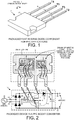
- FIG. 1 is a perspective diagram of a packaged semiconductor device 1 in accordance with one novel aspect.
- Packaged semiconductor device 1 includes a package body portion 2, a first package terminal T1 3, a second package terminal T2 4, a third package terminal T3 5, and a fourth package terminal T4 6.
- the body portion 2 includes a die attach tab 7, an N-channel field effect transistor (NFET) die 8, a fast recovery inverse diode die 9, bond wires 10-16, and an amount of injection-molded encapsulant 17.
- the amount of injection molded plastic encapsulant 17 overmolds and encapsulates the NFET die 9 and the fast recovery inverse diode die 9, the bond wires 10-16, and the die attach tab 7.
- the first package terminal T1 is actually an extension of die attach tab 7.
- the first package terminal T1 and the die attach tab 7 are parts of the same single piece of stamped copper sheet.
- the metal of these terminals is metal of a leadframe and the overmolding or injection-molding with encapsulant (for example, by injection-molded polymerizing resin) is as carried out in conventional semiconductor device injection molding packaging process.
- FIG. 2 is a diagram that illustrates the circuitry inside the packaged semiconductor device 1.
- FIG. 2 also shows how the packaged semiconductor device 1 is used in a 400 volt output voltage PFC AC-to-DC boost converter 18.
- the NFET die 8 has a topside gate electrode and bond pad 19, a topside source electrode and bond pad 20, and a bottomside drain electrode and bond pad 21.
- the fast recovery inverse diode die 9 has a topside cathode electrode and bond pad 22, and a bottomside anode electrode and bond pad 23.
- the topside gate electrode 19 of the NFET die 8 is coupled by bond wire 10 to package terminal T2.
- the topside source electrode 20 of the NFET die 8 is coupled by bond wires 11-13 to package terminal T3.
- the topside cathode electrode 22 of the inverse diode die 9 is coupled by bond wires 14-16 to fourth terminal T4.
- the bottomside drain electrode 21 of NFET die 8 and the bottomside anode terminal 23 of the inverse diode die 9 are both mounted on the die attach tab 7 such that the die attach tab 7 electrically couples the bottomside drain electrode 21 of NFET die 8 to the bottomside anode terminal 23 of the inverse diode die 9.
- NFET die 8 and inverse diode die 9 may, for example, be soldered directly to the die attach tab 7.
- the PFC AC-to-DC boost converter 18 of FIG. 2 has two input terminals 24 and 25 and two output terminals 26 and 27.
- Boost converter 18 receives a 240 volt AC RMS sinusoidal input supply voltage from AC power source 28 onto input terminals 24 and 25.
- the boost converter 18 outputs a 400 volt DC voltage onto the output terminals 26 and 27.
- Boost converter 18 includes a full bridge rectifier involving four diodes 29-32, an inductor 33, the packaged semiconductor device 1, a control circuit 34, and an output capacitor 35, all interconnected as illustrated in FIG. 2 .
- the manufacture of the boost converter 18 is facilitated by the existence of the novel packaged semiconductor device 1.
- NFET die 8 is an N-channel planar-type power field effect transistor that has a breakdown voltage (BV DSS ) of at least 600 volts.
- the inverse diode die 9 is a so-called "inverse diode” in that its anode is on the bottomside of the die and is a P type region, and in that it has a P type isolation structure. This P type isolation structure isolates and separates a central active area of the die from the four die side edges and from the bottom surface of the die.
- the inverse diode die 9 also has all of the following characteristics: 1) a low forward voltage drop (V f ) of less than 1.5 volts in a high current forward conduction condition of 10 amperes, 2) a peak reverse recovery current (I rr ) that is less than 5 amperes when the inverse diode die switches from the high current forward current condition to a -100 volt reverse voltage condition, 3) a reverse breakdown voltage (V br ) withstand capability of at least 550 volts, and 4) a reverse leakage current (I lk ) of less than 100 microamperes in a 450 volt static reverse blocking condition.
- V f low forward voltage drop
- I rr peak reverse recovery current
- V br reverse breakdown voltage
- I lk reverse leakage current
- the inverse diode die 9 achieves these performance characteristics without extra recombination centers having been introduced into the silicon material of the die such as by electron irradiation, or by the inclusion of heavy metal atoms, or by hydrogen or helium ion implantation, or by the inclusion of so-called "lifetime killers".
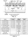
- FIG. 3 is a cross-sectional side view diagram of the NFET die 9.
- An N- type drift region 36 is disposed on an N++ type silicon substrate layer and region 37.
- the P body of the device includes a P type body region portion 38 as well as a more heavily doped P+ type body region 39.
- Reference numeral 40 identifies the N+ type source region 41.
- Reference numeral 42 identifies an N type JFET region.
- Reference numeral 43 identifies an N+ type polysilicon gate. This gate is separated from the top semiconductor surface 44 by gate oxide 45. More oxide 46 is disposed over the gate.
- the bottomside drain electrode 21 is disposed on the bottom semiconductor surface 47.
- the topside source electrode 20 is disposed over the oxide 46.
- the topside gate metal electrode 19 is not present in the particular cross-section of the illustration, so it is not shown.
- FIG. 4 is a table that sets forth concentrations, dopant types, constituent materials, thicknesses and depths for the various parts of the NFET die 9.
- FIG. 5 is a cross-sectional side view diagram of the inverse diode die 9.
- the die 1 has a rectangular top surface, a rectangular bottom surface, and four peripheral side edges. Two of the side edges 48 and 49 are illustrated in the cross-sectional side view diagram of FIG. 5 .
- a bottomside P- type silicon region 50 extends upward from the planar bottom semiconductor surface 51 of the die and also extends laterally outwardly to all four peripheral side edges of the die.
- An N- type silicon region 52 is disposed on and over the bottomside P- type silicon region 50 as shown in FIG. 5 .
- This N- type silicon region 52 which is also referred to as the N- drift region, is of the same bulk wafer material as is the bottomside P- type silicon region 50.
- the N- type silicon region 52 is the cathode of the inverse diode die because the principal PN junction of the diode is the junction between the top of the bottomside P- type silicon region 50 and the bottom of the N- type silicon region 52.
- An N type depletion stopper region 53 extends down from the top semiconductor surface 54 down into the N- type silicon region 52.
- N+ type contact regions extend down from the top semiconductor surface 54 down into the N type depletion stopper region 53 as illustrated.
- a novel P+ type charge carrier extraction region 59 extends down from the top semiconductor surface 54 down into the N type depletion stopper region 53 as illustrated.
- FIG. 6 is a top-down diagram of the P+ type charge carrier extraction region 59 and the N+ type contact regions 55-57, the ring-shaped N+ type depletion stopper region 58, and the N type depletion stopper region 53.
- the top-down diagram of FIG. 6 is a view taken looking down onto the top semiconductor surface of the die.
- the cross-sectional view of FIG. 5 is taken along the sectional line A-A' of FIG. 6 .
- the nine N+ type contact regions are disposed in a two-dimensional array of rows and columns. Each of the nine N+ type contact regions is laterally surrounded by P+ type silicon of the P+ type charge carrier extraction region 59.
- the ring-shaped N+ type depletion stopper region 58 extends around the outer periphery of the P+ type charge carrier extraction region 59.
- the depth of the nine N+ type contact regions, the depth of the ring-shaped N+ type depletion stopper region, and the depth of the P+ type charge carrier extraction region are similar. In this example these depths are in a range of about 0.4 microns to about 0.6 microns.
- the depth of the N type depletion stopper region 53 is about 1.6 microns, where this distance is measured from the top of the N- type region 52 to the bottom of the P+ type charge carrier extraction region 59.
- the N type depletion stopper region 53 is made adequately thicker than the P+ type charge carrier extraction region 59 so that under the desired maximum reverse blocking voltage of the device the principal depletion region (from the PN junction between regions 50 and 52) does not extend upward so far as to reach the depletion region at the PN junction between the bottom of the P+ type charge carrier extraction region 59 and N type silicon of the N type depletion stopper region 53.
- a P+ type floating field ring 63 extends down from the top semiconductor surface 54 down into the N- type silicon region 52 as illustrated. P+ type floating field ring 63 peripherally rings around the central active area of the die where the N type depletion stopper region 53 is located.
- the die also has a P type silicon peripheral sidewall region 60 that extends laterally inwardly from the four peripheral side edges of the die such that it rings around the central N- type silicon region 52.
- the P type silicon peripheral sidewall region 60 extends down and joins the bottomside P- type silicon region 50 and also extends up to the top semiconductor surface 54.
- the combination of the P type peripheral region 60 and the bottomside P- type silicon region 50 form what is called the "P type isolation structure” (also sometimes called the "P type isolation region”, or the "P type separation diffusion structure”, or the "P type separation diffusion region”).
- P type silicon of this structure fully surrounds the N- type silicon region 52 both peripherally from the sides as well as underneath from the bottom.
- the P type separation diffusion structure is made by diffusing aluminum downward from the top semiconductor surface 54 so as to form region 60, and by ion implanting the bottom of the wafer with P type dopants and then activating the dopants by laser annealing to form the region 50.
- Patent No. 6,507,050 entitled Thyristors Having A Novel Arrangement of Concentric Perimeter Zones", filed August 16, 2000, by Green; 8)
- U.S. Patent No. 6,936,908 entitled “Forward and Reverse Blocking Devices", filed March 13, 2002, by Kelberlau et al.; 9)
- U.S. Patent No. 7,030,426 entitled “Power Semiconductor Component in the Planar Technique", filed March 14, 2005, by Nurging; 10)
- An oxide layer 61 is disposed directly on the top semiconductor surface 54 as shown. This oxide layer 61 laterally surrounds a cathode contact portion of the top semiconductor surface.
- the topside metal electrode 22 is disposed directly on the cathode contact portion of the top semiconductor surface 54 as illustrated.
- the topside metal electrode 22 is a cathode electrode or a cathode terminal of the inverse diode device.
- the bottomside metal electrode 23 is disposed directly on the bottom semiconductor surface 51 of the die. This bottomside metal electrode 23 extends all across the bottom semiconductor surface 51 from the die side edge 48 to the die side edge 49. Bottomside metal electrode 23 as well as the bottomside P- type region 50 are much wider than the topside metal electrode 22.
- Bottomside metal electrode 23 is the anode electrode or the anode terminal of the inverse diode device.
- a topside passivation layer 62 is disposed over the oxide layer 61 so that passivation overlaps and covers the peripheral edges of the topside metal electrode 22. All silicon regions between the bottom semiconductor surface 51 and the top semiconductor surface 54 are bulk silicon wafer material. There is no epitaxial silicon material.
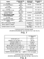
- FIG. 7 is a table that sets forth dopant concentrations, dopant types and dimensions of various parts of the inverse diode device die 9.
- FIG. 8 is a table that sets forth operational characteristics of the inverse diode device die 9 of FIG. 5 that includes the novel P+ type charge carrier extraction region 59.
- the data in the table was obtained using the device simulator called Synopsys Sentaurus Workbench (SWB).
- SWB Synopsys Sentaurus Workbench
- the structure of the inverse diode of FIGS. 5-7 was first defined using the 2-D Sentaurus Structure Editor (SDE). The defined structure was then simulated using the device simulator (Sdevice) part of the workbench tool suite.
- SDE 2-D Sentaurus Structure Editor
- FIG. 9 is a cross-sectional diagram that illustrates an operation of the inverse diode device die 9 in a forward bias situation.
- FIG. 10 shows a portion of the die of FIG. 9 in an enlarged fashion.
- the forward bias condition current flows from the anode electrode 23 on the bottom, up through the device, and out of the cathode electrode 22 on the top.
- the voltage polarity across the diode is quickly reversed to a reverse blocking condition, the large number of electrons and holes in these regions 52 and 53 must somehow be eliminated before the diode can begin blocking current flow.
- a depletion region 64 exists at the boundary or boundaries between the P+ type charge carrier extraction region 59 and the N type depletion stopper region 53. This depletion region 64 is illustrated in FIG. 10 .
- the depletion region 64 sets up an electric field 65 across the depletion region. The direction of this electric field 65 is indicated by the arrow 65.
- Charge neutrality is maintained in region 53 and region 52, so electrons are expelled from the bottom of the device.
- Arrow 69 in FIG. 10 illustrates the path of one such representative electron 70.
- This flow of electrons is also continuous as the diode operates in its forward conduction mode.
- the flow of electrons reduces the concentration of electrons in the regions 53 and 52 of the device in the forward bias condition (as compared to the concentration of electrons that otherwise would be present were the P+ type charge carrier extraction regions not present). Due to the attendant reduction in the number of holes and electrons in the regions 53 and 52, there are fewer charge carriers to be removed from the diode when the diode is quickly switched from a forward conduction condition to a reverse voltage condition.
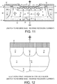
- FIG. 11 is a cross-sectional diagram that illustrates an operation of the inverse diode device 9 when the diode device is switched from the forward bias condition to a reverse bias condition.
- FIG. 12 shows a portion of the inverse diode device die of FIG. 11 in an enlarged fashion.
- FIG. 12 illustrates how these escaping electrons pass up through the N+ type contact regions on their way to the cathode electrode 22.
- the magnitude of the reverse recovery current I rr begins to decrease.
- the diode device then starts to operate in what is referred to here as its "static reverse blocking mode" of operation.
- the amount of reverse current flowing due to the reverse polarity across the diode device in a long term static condition referred to as the reverse leakage current (I lk ), is small.
- One conventional way to make a fast recovery diode is to reduce the lifetime of charge carriers present in the region of the diode where there are such charge carriers. This reduction in carrier lifetime can be accomplished by introducing so-called "recombination centers" into the silicon in the central drift region of the diode. These recombination centers are generally introduced by forming defects in the silicon through ion implantation, and/or by depositing ions or atoms into the silicon crystal lattice. Such recombination centers are generally beneficial during the short time of switching from the forward bias condition to the reverse bias condition because some electrons and holes present in the diode at that time can recombine.
- the diode device uses the P+ type charge carrier extraction region 59 to reduce charge carrier concentrations.
- the silicon of the N- type silicon region 52 need not be implanted or damaged in order to create lifetime killer recombination centers.
- the inverse diode die 9 therefore exhibits both good reverse recovery characteristics as well as a low reverse leakage current.
- FIG. 13 is a waveform that illustrates a diode current waveform 75 during a switching episode of the inverse diode device die 9.
- a forward current of 10 amperes is conducted through the diode device die.
- V f forward voltage drop
- the voltage polarity across the diode device die is then quickly switched so that diode device die 9 blocks current flow.
- the time T zz is defined here as the time from when the reverse recovery current I rr through the diode (when transitioning from a forward conduction condition to a reverse blocking condition) first drops to a negative current until it again rises and reaches zero current.
- the peak of the reverse recovery current (I rr(PEAK) ) occurs between these two zero crossing times.
- the time T zz is the time interval between zero crossings of the reverse current during this reverse commutation episode.
- the inverse diode device die There is no epitaxial silicon in the inverse diode device die 9. Long term dynamic ruggedness of the device may be improved due to the absence of any epitaxial silicon to oxide/passivation interface in the edge termination region of the device.
- topside processing is performed on an N- type wafer. After the topside passivation step, the wafer is thinned by backside grinding. P type dopants are implanted into the bottom thinned side of the wafer, and the P type dopants are activated by laser annealing. After bottomside metallization, the wafer is diced. Accordingly, there is no epitaxial silicon in the device. In another example, the inverse diode device die does have epitaxial silicon. The starting material is a P type wafer.
- N- type epitaxial silicon is grown on the wafer. After topside processing and topside passivation, the wafer is thinned by backside grinding. After bottomside metallization, the wafer is diced.
- the inverse diode device die 9 of the packaged semiconductor device 1 of FIG. 1 can be of either construction as long as it includes the novel P+ type charge carrier extraction region 59.
- the thickness of the N- type region 52 of the resulting inverse diode device die 9 of FIG. 5 is reduced down to 28 microns, where this distance is measured from the top of the bottomside P- type region 50 to the bottom of the N type depletion stop region 53.
- the thickness of the N type depletion stop region 53 is 1.6 microns, where this distance is measured from the top of the N- type region 52 to the bottom of the P+ type charge carrier extraction region 59.
- the thickness of the P+ type charge carrier extraction region 59 is 0.4 microns, where this distance is measured from the top of the N type depletion stop region 53 to the top semiconductor surface 54.
- the overall thickness of the thinned wafer is 33 microns where this distance is measured from the bottom semiconductor surface 51 to the top semiconductor surface 54.
- PFC Power Factor Correction
- the diode die 9 must withstand a reverse voltage of about 400 volts.
- the voltage rating of the device is 70 percent of its actual breakdown voltage, so a properly rate diode device die would have to have a breakdown voltage of about 550 volts. But in addition, another ten percent margin is required for manufacturability.
- the inverse diode device die 9 in the circuit of FIG. 2 is made to have a reverse breakdown rating of about 550 volts, and a target reverse breakdown voltage of 600 volts.
- the wafer during diode manufacture is adequately thinned from its backside such that the resulting thickness of the N- type region 52 is about 28 microns.
- the advantages of the novel P+ type charge carrier extraction region 53 is applied to the PFC boost converter application of FIG. 2 .
- reverse leakage current through the inverse diode die 9 increases.
- the novel inverse diode device die 9 nonetheless still has a desirably low reverse leakage current while at the same time maintaining its "fast" nature (low I rr(PEAK) ) for the switching condition to which the diode die is subjected.
- the NFET die and the inverse diode die are mounted to a die attach tab
- the NFET die and the inverse diode die can be mounted to another type of substrate.
- the first package terminal can be an extension of the die attach tab.
- the die attach tab and the first package terminal can be parts of the same piece of stamped metal, such as a part of a metal leadframe.
- the substrate is a separate structure and the first package terminal is electrically coupled to the separate structure (for example, by a bond wire).
- the first package terminal can also be bonded to the separate structure.
- the package body may involve injection molded plastic as described above, but it may also involve another type of encapsulating structure and material.
- a part or a surface of the substrate is not covered by encapsulant so that this part or surface can better dissipate heat. Even though the substrate is not entirely encased by encapsulant, the encapsulant nevertheless encapsulates the NFET and the inverse diode on the substrate. Accordingly, various modifications, adaptations, and combinations of various features of the described embodiments can be practiced without departing from the scope of the invention as set forth in the claims.
Landscapes
- Engineering & Computer Science (AREA)
- Power Engineering (AREA)
- Electrodes Of Semiconductors (AREA)
- Metal-Oxide And Bipolar Metal-Oxide Semiconductor Integrated Circuits (AREA)
- Semiconductor Integrated Circuits (AREA)
- Physics & Mathematics (AREA)
- Geometry (AREA)
- Microelectronics & Electronic Packaging (AREA)
- Rectifiers (AREA)
Abstract
Description
- The described embodiments relate to inverse diode devices and to related methods.
- Most all types of commercially-available power diodes that have high reverse breakdown voltage capabilities also have N-type bottomside cathodes. A rare exception is the so-called "inverse diode" or "reverse diode" that is commercially available from IXYS Corporation, 1590 Buckeye Drive, Milpitas, California. These unusual diodes have P type isolation structures involving a bottomside P type anode region as well as P type peripheral sidewall diffusion regions. These unusual diodes have a few superior characteristics as compared to other types of diodes. For example, they may have high reverse breakdown voltages while simultaneously exhibiting superior dynamic robustness. Ways of extending this inverse diode architecture into new areas of application are sought.
- A four-terminal packaged semiconductor device has a first package terminal T1, a second package terminal T2, a third package terminal T3, a fourth package terminal T4, and a package body. Within the package body is a die attach tab, an N-channel field effect transistor (NFET) die and a novel fast recovery inverse diode device die. The NFET die and the fast recovery inverse diode die are mounted to the die attach tab within the package body such that a bottomside drain electrode of the NFET die is electrically coupled via the die attach tab to a bottomside P type anode region of the inverse diode die. The NFET die, the fast recovery inverse diode die, and the die attach tab are typically overmolded with an amount of injection molded encapsulant. The first package terminal T1 is coupled to, or is a part of, the die attach tab. The second package terminal T2 is coupled to a topside gate electrode of the NFET die. The third package terminal T3 is coupled to a topside source electrode of the NFET die. The fourth package terminal T4 is coupled to a topside cathode electrode of the inverse diode die.
- The fast recovery inverse diode die is an "inverse diode" in that its anode is on the bottomside of the die and is a P type region, and in that it has a P type isolation structure. The P type isolation structure isolates and separates a central active area of the die from the four die side edges and from the bottom semiconductor surface of the die. The fast recovery inverse diode die also has all of the following characteristics: 1) a low forward voltage drop (Vf) of less than 1.5 volts in a high current forward conduction condition of 10 amperes, 2) a peak reverse recovery current (Irr) that is less than 5 amperes when the inverse diode die switches from the high current forward current condition to a -100 volt reverse voltage condition, 3) a reverse breakdown voltage (Vbr) withstand capability of at least 550 volts, and 4) a reverse leakage current (Ilk) of less than 100 microamperes in a 450 volt static reverse blocking condition. The NFET die is a planar N-channel power MOSFET that has a breakdown voltage (BVDSS) of at least 600 volts. The novel packaged semiconductor device is particularly advantageous and convenient when used in a 400 volt DC output voltage PFC (Power Factor Correction) boost converter circuit.
- The disclosure includes the following clauses:
- 1. A packaged semiconductor device comprising:
- a first package terminal;
- a die attach tab, wherein the die attach tab is coupled to the first package terminal;
- an N-channel field effect transistor (NFET) die, wherein the NFET die has a topside gate electrode, a topside source electrode, and a bottomside drain electrode, wherein the bottomside drain electrode is mounted to the die attach tab;
- an inverse diode die, wherein the inverse diode die comprises:
- a bottomside P type silicon region that extends upward from a bottom semiconductor surface of the inverse diode die that also extends laterally outwardly to peripheral side edges of the inverse diode die;
- an N- type silicon region disposed over the bottomside P type silicon region;
- an N type depletion stopper region that extends downward from the top semiconductor surface and into the N- type silicon region;
- a P+ type charge carrier extraction region that extends downward from the top semiconductor surface and into the N type depletion stopper region;
- an N+ type contact region that extends downward from the top semiconductor surface and into the N type depletion stopper region;
- a P type silicon peripheral sidewall region that extends downward from the top semiconductor surface into the N- type silicon region, wherein the P type silicon peripheral sidewall region joins the bottomside P type silicon region thereby forming a P type isolation structure, wherein the P type silicon peripheral sidewall region also laterally rings the N- type silicon region and separates the N-type silicon region from the peripheral side edges of the inverse diode die;
- a topside cathode electrode disposed on the N+ type contact region and on the P+ type charge carrier extraction region; and
- a bottomside anode electrode disposed on the bottom semiconductor surface of the inverse diode die, wherein the bottomside anode electrode is mounted to the die attach tab;
- a second package terminal that is coupled to the topside gate electrode of the NFET die;
- a third package terminal that is coupled to the topside source electrode of the NFET die;
- a fourth package terminal that is coupled to the topside cathode electrode of the inverse diode die; and
- an amount of encapsulant that encapsulates the NFET die and the inverse diode die on the die attach tab portion of the first package terminal and die attach tab.
- 2. The packaged semiconductor device of
clause 1, wherein the inverse diode die has a reverse leakage current (Ilk) of less than 100 microamperes in a 450 volt static reverse blocking condition. - 3. The packaged semiconductor device of
clause 1, wherein the first package terminal is an extension of the die attach tab, wherein the first package terminal and the die attach tab are two parts of a single piece of stamped metal. - 4. The packaged semiconductor device of
clause 1, wherein the first package terminal is bonded to the die attach tab. - 5. The packaged semiconductor device of
clause 1, wherein the first package terminal is coupled to the die attach tab via a bond wire. - 6. The packaged semiconductor device of
clause 1, wherein the packaged semiconductor device has four and no more than four package terminals. - 7. The packaged semiconductor device of
clause 1, wherein the inverse diode die has all of the following: 1) a low forward voltage drop (Vf) of less than 1.5 volts in a high current forward conduction condition of 10 amperes, 2) a peak reverse recovery current (Irr) that is less than 5 amperes when the inverse diode die switches from the high current forward current condition to a 100 volt reverse voltage condition, 3) a reverse breakdown voltage (Vbr) withstand capability of at least 550 volts, and 4) a reverse leakage current (Ilk) of less than 100 microamperes in a 450 volt static reverse blocking condition. - 8. The packaged semiconductor device of
clause 1, wherein the NFET die has a breakdown voltage (BVDSS) of at least 550 volts. - 9. A packaged semiconductor device comprising:
- a first package terminal;
- a die attach tab, wherein the die attach tab is coupled to the first package terminal;
- an N-channel field effect transistor (NFET) die, wherein the NFET die has a topside gate electrode, a topside source electrode, and a bottomside drain electrode, wherein the bottomside drain electrode is mounted to the die attach tab;
- an inverse diode die, wherein the inverse diode die has a topside cathode electrode, a bottomside P type silicon region and a bottomside anode electrode, wherein the bottomside anode electrode is mounted to the die attach tab, wherein the die attach tab electrically couples the bottomside drain electrode of the NFET to the bottomside anode electrode of the inverse diode die;
- a second package terminal that is coupled to the topside gate electrode of the NFET die;
- a third package terminal that is coupled to the topside source electrode of the NFET die;
- a fourth package terminal that is coupled to the topside cathode electrode of the inverse diode die; and
- an amount of encapsulant that encapsulates the NFET die and the inverse diode die on the die attach tab portion of the first package terminal and die attach tab.
- 10. The packaged semiconductor device of clause 9, wherein the first package terminal is an extension of the die attach tab, wherein the first package terminal and the die attach tab are two parts of a single piece of stamped metal.
- 11. The packaged semiconductor device of clause 9, wherein the first package terminal is bonded to the die attach tab.
- 12. The packaged semiconductor device of clause 9, wherein the first package terminal is coupled to the die attach tab via a bond wire.
- 13. The packaged semiconductor device of clause 9, wherein the inverse diode die has a top semiconductor surface, the inverse diode die further comprising:
- an N type depletion stopper region that extends downward from the top semiconductor surface and into an N- type silicon region;
- a P+ type charge carrier extraction region that extends downward from the top semiconductor surface and into the N type depletion stopper region; and
- an N+ type contact region that extends downward from the top semiconductor surface and into the N type depletion stopper region, wherein the topside cathode electrode is coupled to both the P+ type charge carrier extraction region and the N+ type contact region.
- 14. The packaged semiconductor device of clause 9, wherein the inverse diode die has a reverse leakage current (Ilk) of less than 100 microamperes in a 450 volt static reverse blocking condition.
- 15. The packaged semiconductor device of clause 9, wherein the inverse diode die has all of the following: 1) a low forward voltage drop (Vf) of less than 1.5 volts in a high current forward conduction condition of 10 amperes, 2) a peak reverse recovery current (Irr) that is less than 5 amperes when the inverse diode die switches from the high current forward current condition to a 100 volt reverse voltage condition, 3) a reverse breakdown voltage (Vbr) withstand capability of at least 550 volts, and 4) a reverse leakage current (Ilk) of less than 100 microamperes in a 450 volt static reverse blocking condition.
- 16. The packaged semiconductor device of clause 9, wherein the packaged semiconductor device has four and no more than four package terminals.
- 17. A packaged semiconductor device comprising:
- a first package terminal;
- a substrate having a conductive surface, wherein the conductive surface is coupled to the first package terminal;
- an N-channel field effect transistor (NFET) die, wherein the NFET die has a topside gate electrode, a topside source electrode, and a bottomside drain electrode, wherein the bottomside drain electrode is mounted to the substrate;
- means for conducting a current in a forward voltage condition and for blocking current flow in a reverse voltage condition, wherein the means has a topside metal electrode and a bottomside metal electrode, wherein the bottomside metal electrode is mounted to the substrate, wherein the means is for: 1) conducting a forward current with a forward voltage drop of less than 1.5 volts in a 10 ampere forward conduction condition, 2) switching from the forward conduction condition to a 100 volt reverse voltage condition without conducting a reverse recovery current of more than 5 amperes, 3) withstanding a reverse voltage of at least 550 volts without suffering reverse breakdown, and 4) withstanding a 450 volt static reverse blocking condition without conducting a reverse leakage current of more than 100 microamperes;
- a second package terminal that is coupled to the topside gate electrode of the NFET die;
- a third package terminal that is coupled to the topside source electrode of the NFET die;
- a fourth package terminal that is coupled to the topside metal electrode of the means; and
- an amount of encapsulant that encapsulates the NFET die and the means on the substrate.
- 18. The packaged semiconductor device of
clause 17, wherein the first package terminal is an extension of the substrate, wherein the first package terminal and the substrate are two parts of a single piece of stamped metal. - 19. The packaged semiconductor device of
clause 17, wherein the first package terminal is bonded to the substrate. - 20. The packaged semiconductor device of
clause 17, wherein the first package terminal is coupled to the substrate via a bond wire. - 21. Use of a packaged semiconductor device according to any of the preceding clauses in a power factor correction (PFC) application.
- Further details and embodiments and methods are described in the detailed description below. This summary does not purport to define the invention. The invention is defined by the claims.
- The accompanying drawings, where like numerals indicate like components, illustrate embodiments of the invention.
-
FIG. 1 is a perspective diagram of a packaged semiconductor device in accordance with one novel aspect. -
FIG. 2 is a diagram that illustrates the circuitry inside the packaged semiconductor device ofFIG. 1 and also shows how the packaged semiconductor device ofFIG. 1 is used in a PFC AC-to-DC boost converter circuit. -
FIG. 3 is a cross-sectional side view diagram of the NFET die within the packaged semiconductor device ofFIG. 1 . -
FIG. 4 is a table that sets forth concentrations, dopant types, constituent materials, thicknesses and depths for the various parts of the NFET die ofFIG. 3 . -
FIG. 5 is a cross-sectional side view diagram of the inverse diode die within the packaged semiconductor device ofFIG. 1 . -
FIG. 6 is a top-down diagram of the P+ type charge carrier extraction region of the inverse diode device die ofFIG. 5 . -
FIG. 7 is a table that sets forth concentrations, dopant types, constituent materials, thicknesses and depths for the various parts of the inverse diode device die ofFIG. 5 . -
FIG. 8 is a table that sets forth operational characteristics of the inverse diode device die ofFIG. 5 . -
FIG. 9 is a cross-sectional side view diagram of the inverse diode device die ofFIG. 5 in a forward conduction situation. -
FIG. 10 shows a portion ofFIG. 9 in an enlarged fashion. -
FIG. 11 is a cross-sectional side view diagram that illustrates an operation of the inverse diode device die ofFIG. 5 when the voltage polarity across the diode device die is quickly switched from the forward conduction condition to a reverse blocking condition. -
FIG. 12 shows a portion of the inverse diode device die ofFIG. 11 in an enlarged fashion. -
FIG. 13 is a waveform diagram that illustrates the time Tzz. - Reference will now be made in detail to background examples and some embodiments of the invention, examples of which are illustrated in the accompanying drawings. In the description and claims below, when a first object is referred to as being disposed "over" or "on" a second object, it is to be understood that the first object can be directly on the second object, or an intervening object may be present between the first and second objects. Similarly, terms such as "top", "topside", "up", "upward", "down", "downward", "vertically", "laterally", "side", "under", "backside", "bottom" and "bottomside" are used herein to describe relative orientations between different parts of the structure being described, and it is to be understood that the overall structure being described can actually be oriented in any way in three-dimensional space. When processing is described in the description below as being performed on the bottom of the wafer, such as for example when dopants are said to diffuse upward, it is understood the wafer may actually be oriented upside down during these processing steps, and may be processed from the top in ordinary fashion. In the description below, P type silicon can be generally referred to simply as P type silicon or it can be more specifically referred to as P++ type silicon, P+ type silicon, P type silicon, or P- type silicon. The P++, P+, P and P- designators are intended to designate relative ranges of dopant concentrations in a rough general sense. There may, for example, be an overlap in the ranges of concentrations between silicon described as P+ type silicon and silicon described as P type silicon. The dopant concentration at the bottom of the P+ type silicon range may be lower than the dopant concentration at the top of the P type silicon range. The same manner of describing N type silicon (in terms of sometimes more specifically referring to N+ type silicon, N type silicon, or N- type silicon) is also employed in this patent document.
-
FIG. 1 is a perspective diagram of a packagedsemiconductor device 1 in accordance with one novel aspect. Packagedsemiconductor device 1 includes apackage body portion 2, a firstpackage terminal T1 3, a secondpackage terminal T2 4, a thirdpackage terminal T3 5, and a fourthpackage terminal T4 6. Thebody portion 2 includes a die attachtab 7, an N-channel field effect transistor (NFET) die 8, a fast recovery inverse diode die 9, bond wires 10-16, and an amount of injection-moldedencapsulant 17. The amount of injection moldedplastic encapsulant 17 overmolds and encapsulates the NFET die 9 and the fast recovery inverse diode die 9, the bond wires 10-16, and the die attachtab 7. In this example, the first package terminal T1 is actually an extension of die attachtab 7. The first package terminal T1 and the die attachtab 7 are parts of the same single piece of stamped copper sheet. The metal of these terminals is metal of a leadframe and the overmolding or injection-molding with encapsulant (for example, by injection-molded polymerizing resin) is as carried out in conventional semiconductor device injection molding packaging process. -
FIG. 2 is a diagram that illustrates the circuitry inside the packagedsemiconductor device 1.FIG. 2 also shows how the packagedsemiconductor device 1 is used in a 400 volt output voltage PFC AC-to-DC boost converter 18. The NFET die 8 has a topside gate electrode andbond pad 19, a topside source electrode andbond pad 20, and a bottomside drain electrode andbond pad 21. The fast recovery inverse diode die 9 has a topside cathode electrode andbond pad 22, and a bottomside anode electrode andbond pad 23. Thetopside gate electrode 19 of the NFET die 8 is coupled bybond wire 10 to package terminal T2. Thetopside source electrode 20 of the NFET die 8 is coupled by bond wires 11-13 to package terminal T3. Thetopside cathode electrode 22 of the inverse diode die 9 is coupled by bond wires 14-16 to fourth terminal T4. Importantly, thebottomside drain electrode 21 of NFET die 8 and thebottomside anode terminal 23 of the inverse diode die 9 are both mounted on the die attachtab 7 such that the die attachtab 7 electrically couples thebottomside drain electrode 21 of NFET die 8 to thebottomside anode terminal 23 of the inverse diode die 9. NFET die 8 and inverse diode die 9 may, for example, be soldered directly to the die attachtab 7. - The PFC AC-to-
DC boost converter 18 ofFIG. 2 has twoinput terminals output terminals 26 and 27.Boost converter 18 receives a 240 volt AC RMS sinusoidal input supply voltage fromAC power source 28 ontoinput terminals boost converter 18 outputs a 400 volt DC voltage onto theoutput terminals 26 and 27.Boost converter 18 includes a full bridge rectifier involving four diodes 29-32, aninductor 33, the packagedsemiconductor device 1, acontrol circuit 34, and anoutput capacitor 35, all interconnected as illustrated inFIG. 2 . The manufacture of theboost converter 18 is facilitated by the existence of the novel packagedsemiconductor device 1. - NFET die 8 is an N-channel planar-type power field effect transistor that has a breakdown voltage (BVDSS) of at least 600 volts. The inverse diode die 9 is a so-called "inverse diode" in that its anode is on the bottomside of the die and is a P type region, and in that it has a P type isolation structure. This P type isolation structure isolates and separates a central active area of the die from the four die side edges and from the bottom surface of the die. The inverse diode die 9 also has all of the following characteristics: 1) a low forward voltage drop (Vf) of less than 1.5 volts in a high current forward conduction condition of 10 amperes, 2) a peak reverse recovery current (Irr) that is less than 5 amperes when the inverse diode die switches from the high current forward current condition to a -100 volt reverse voltage condition, 3) a reverse breakdown voltage (Vbr) withstand capability of at least 550 volts, and 4) a reverse leakage current (Ilk) of less than 100 microamperes in a 450 volt static reverse blocking condition. In one example, the inverse diode die 9 achieves these performance characteristics without extra recombination centers having been introduced into the silicon material of the die such as by electron irradiation, or by the inclusion of heavy metal atoms, or by hydrogen or helium ion implantation, or by the inclusion of so-called "lifetime killers".
-
FIG. 3 is a cross-sectional side view diagram of the NFET die 9. An N-type drift region 36 is disposed on an N++ type silicon substrate layer andregion 37. The P body of the device includes a P typebody region portion 38 as well as a more heavily doped P+type body region 39. Reference numeral 40 identifies the N+type source region 41.Reference numeral 42 identifies an N type JFET region.Reference numeral 43 identifies an N+ type polysilicon gate. This gate is separated from thetop semiconductor surface 44 bygate oxide 45.More oxide 46 is disposed over the gate. Thebottomside drain electrode 21 is disposed on thebottom semiconductor surface 47. Thetopside source electrode 20 is disposed over theoxide 46. The topsidegate metal electrode 19 is not present in the particular cross-section of the illustration, so it is not shown. -
FIG. 4 is a table that sets forth concentrations, dopant types, constituent materials, thicknesses and depths for the various parts of the NFET die 9. -
FIG. 5 is a cross-sectional side view diagram of the inverse diode die 9. Thedie 1 has a rectangular top surface, a rectangular bottom surface, and four peripheral side edges. Two of the side edges 48 and 49 are illustrated in the cross-sectional side view diagram ofFIG. 5 . More particularly, a bottomside P-type silicon region 50 extends upward from the planarbottom semiconductor surface 51 of the die and also extends laterally outwardly to all four peripheral side edges of the die. An N-type silicon region 52 is disposed on and over the bottomside P-type silicon region 50 as shown inFIG. 5 . This N-type silicon region 52, which is also referred to as the N- drift region, is of the same bulk wafer material as is the bottomside P-type silicon region 50. The N-type silicon region 52 is the cathode of the inverse diode die because the principal PN junction of the diode is the junction between the top of the bottomside P-type silicon region 50 and the bottom of the N-type silicon region 52. An N typedepletion stopper region 53 extends down from thetop semiconductor surface 54 down into the N-type silicon region 52. N+ type contact regions extend down from thetop semiconductor surface 54 down into the N typedepletion stopper region 53 as illustrated. There are three N+ type contact regions 55-57 in the particular cross-section illustrated inFIG. 5 . There is also a ring-shaped N+ typedepletion stopper region 58. A novel P+ type chargecarrier extraction region 59 extends down from thetop semiconductor surface 54 down into the N typedepletion stopper region 53 as illustrated. -
FIG. 6 is a top-down diagram of the P+ type chargecarrier extraction region 59 and the N+ type contact regions 55-57, the ring-shaped N+ typedepletion stopper region 58, and the N typedepletion stopper region 53. The top-down diagram ofFIG. 6 is a view taken looking down onto the top semiconductor surface of the die. The cross-sectional view ofFIG. 5 is taken along the sectional line A-A' ofFIG. 6 . As can be seen from the top-down view ofFIG. 6 , the nine N+ type contact regions are disposed in a two-dimensional array of rows and columns. Each of the nine N+ type contact regions is laterally surrounded by P+ type silicon of the P+ type chargecarrier extraction region 59. The ring-shaped N+ typedepletion stopper region 58 extends around the outer periphery of the P+ type chargecarrier extraction region 59. The depth of the nine N+ type contact regions, the depth of the ring-shaped N+ type depletion stopper region, and the depth of the P+ type charge carrier extraction region are similar. In this example these depths are in a range of about 0.4 microns to about 0.6 microns. The depth of the N typedepletion stopper region 53 is about 1.6 microns, where this distance is measured from the top of the N-type region 52 to the bottom of the P+ type chargecarrier extraction region 59. The N typedepletion stopper region 53 is made adequately thicker than the P+ type chargecarrier extraction region 59 so that under the desired maximum reverse blocking voltage of the device the principal depletion region (from the PN junction betweenregions 50 and 52) does not extend upward so far as to reach the depletion region at the PN junction between the bottom of the P+ type chargecarrier extraction region 59 and N type silicon of the N typedepletion stopper region 53. A P+ type floatingfield ring 63 extends down from thetop semiconductor surface 54 down into the N-type silicon region 52 as illustrated. P+ type floatingfield ring 63 peripherally rings around the central active area of the die where the N typedepletion stopper region 53 is located. - The die also has a P type silicon
peripheral sidewall region 60 that extends laterally inwardly from the four peripheral side edges of the die such that it rings around the central N-type silicon region 52. The P type siliconperipheral sidewall region 60 extends down and joins the bottomside P-type silicon region 50 and also extends up to thetop semiconductor surface 54. The combination of the P typeperipheral region 60 and the bottomside P-type silicon region 50 form what is called the "P type isolation structure" (also sometimes called the "P type isolation region", or the "P type separation diffusion structure", or the "P type separation diffusion region"). P type silicon of this structure fully surrounds the N-type silicon region 52 both peripherally from the sides as well as underneath from the bottom. In one example, the P type separation diffusion structure is made by diffusing aluminum downward from thetop semiconductor surface 54 so as to formregion 60, and by ion implanting the bottom of the wafer with P type dopants and then activating the dopants by laser annealing to form theregion 50. - For additional information on various suitable different P type separation diffusion structures and how to form them, see: 1)
U.S Patent No. 7,442,630 , entitled "Method For Fabricating Forward And Reverse Blocking Devices", filed August 30, 2005, by Kelberlau et al.; 2)U.S. Patent No. 5,698,454 , entitled "Method Of Making A Reverse Blocking IGBT", filed July 31, 1995, by N. Zommer; 3) J. Lutz et al., "Semiconductor Power Devices", pages 146-147, published by Springer, Berlin and Heidelberg (2011); 4) the data sheet entitled "Diode Chip", DWN 17-18, by IXYS Corporation of Milpitas, California 95035, USA; 5)U.S. Patent No. 9,590,033 U.S. Patent No. 4,351,677 , entitled "Method of Manufacturing Semiconductor Device Having Aluminum Diffused Semiconductor Substrate", filed July 10, 1980, by Mochizuki et al.; 7)U.S. Patent No. 6,507,050 , entitled Thyristors Having A Novel Arrangement of Concentric Perimeter Zones", filed August 16, 2000, by Green; 8)U.S. Patent No. 6,936,908 , entitled "Forward and Reverse Blocking Devices", filed March 13, 2002, by Kelberlau et al.; 9)U.S. Patent No. 7,030,426 , entitled "Power Semiconductor Component in the Planar Technique", filed March 14, 2005, by Neidig; 10)U.S. Patent No. 8,093,652 , entitled "Breakdown Voltage For Power Devices", filed August 27, 2003, by Veeramma et al.; 11) the 2004 description entitled "FRED, Rectifier Diode and Thyristor Chips in Planar Design", by IXYS Semiconductor GmbH, Edisonstrasse 15, D-68623, Lampertheim, Germany; 12)U.S. Patent No. 8,716,067 , entitled "Power Device Manufacture On The Recessed Side Of A Thinned Wafer", filed February 20, 2012, by Wisotzki et al.;U.S. Patent No. 8,716,745 , entitled "Stable Diodes For Low And High Frequency Applications", filed May 11, 2006, by Veeramma. The entire subject matter of each of the following documents is incorporated herein by reference: 1)U.S Patent No. 7,442,630 ; 2)U.S. Patent No. 5,698,454 ; 3)U.S. Patent No. 9,590,033 U.S. Patent No. 4,351,677 ; 5)U.S. Patent No. 6,507,050 ; 6)U.S. Patent No. 6,936,908 ; 7)U.S. Patent No. 7,030,426 ; 8)U.S. Patent No. 8,093,652 ; 9)U.S. Patent No. 8,716,067 ; 10)U.S. Patent No. 8,716,745 . - An
oxide layer 61 is disposed directly on thetop semiconductor surface 54 as shown. Thisoxide layer 61 laterally surrounds a cathode contact portion of the top semiconductor surface. Thetopside metal electrode 22 is disposed directly on the cathode contact portion of thetop semiconductor surface 54 as illustrated. Thetopside metal electrode 22 is a cathode electrode or a cathode terminal of the inverse diode device. Thebottomside metal electrode 23 is disposed directly on thebottom semiconductor surface 51 of the die. Thisbottomside metal electrode 23 extends all across thebottom semiconductor surface 51 from thedie side edge 48 to thedie side edge 49.Bottomside metal electrode 23 as well as the bottomside P-type region 50 are much wider than thetopside metal electrode 22.Bottomside metal electrode 23 is the anode electrode or the anode terminal of the inverse diode device. Atopside passivation layer 62 is disposed over theoxide layer 61 so that passivation overlaps and covers the peripheral edges of thetopside metal electrode 22. All silicon regions between thebottom semiconductor surface 51 and thetop semiconductor surface 54 are bulk silicon wafer material. There is no epitaxial silicon material. -
FIG. 7 is a table that sets forth dopant concentrations, dopant types and dimensions of various parts of the inverse diode device die 9. -
FIG. 8 is a table that sets forth operational characteristics of the inverse diode device die 9 ofFIG. 5 that includes the novel P+ type chargecarrier extraction region 59. The data in the table was obtained using the device simulator called Synopsys Sentaurus Workbench (SWB). The structure of the inverse diode ofFIGS. 5-7 was first defined using the 2-D Sentaurus Structure Editor (SDE). The defined structure was then simulated using the device simulator (Sdevice) part of the workbench tool suite. -
FIG. 9 is a cross-sectional diagram that illustrates an operation of the inverse diode device die 9 in a forward bias situation.FIG. 10 shows a portion of the die ofFIG. 9 in an enlarged fashion. In the forward bias condition, current flows from theanode electrode 23 on the bottom, up through the device, and out of thecathode electrode 22 on the top. During this time, there exists a high concentration of charge carriers inregions regions regions depletion region 64 exists at the boundary or boundaries between the P+ type chargecarrier extraction region 59 and the N typedepletion stopper region 53. Thisdepletion region 64 is illustrated inFIG. 10 . Thedepletion region 64 sets up anelectric field 65 across the depletion region. The direction of thiselectric field 65 is indicated by thearrow 65. Holes that happen to be close to or at the boundary of thedepletion region 64 are swept across thedepletion region 64 in the direction of thearrow 65 due to this localized charge extracting electric field.Arrow 67 inFIG. 10 illustrates the path of one suchrepresentative hole 68. The extraction of holes is continuous as the diode operates in its forward conduction mode. The continuous extraction of holes by the localized charge extractingelectric field 64 reduces the concentration of holes in theregions region 53 andregion 52, so electrons are expelled from the bottom of the device. Arrow 69 inFIG. 10 illustrates the path of one such representative electron 70. This flow of electrons is also continuous as the diode operates in its forward conduction mode. The flow of electrons reduces the concentration of electrons in theregions regions -
FIG. 11 is a cross-sectional diagram that illustrates an operation of the inverse diode device 9 when the diode device is switched from the forward bias condition to a reverse bias condition.FIG. 12 shows a portion of the inverse diode device die ofFIG. 11 in an enlarged fashion. There is adepletion region 71 at the PN junction between the bottomside P-type silicon region 50 and the N-type silicon region 52. When the potential across the diode device is reversed, thedepletion region 71 expands. It expands downward, but it expands far more upward due to the lower concentration in the N-silicon region. Thisdepletion region 71 sets up anelectric field 72. Holes from the expandingdepletion region 71 move downward through the bottomside P-type silicon region 50 toward theanode electrode 23.Arrow 73 inFIG. 11 represents the path of one representative one of these holes. Electrons from the expandingdepletion region 71 move upward through the N-type silicon region 52.Arrow 74 inFIG. 12 represents the path of one representative one of these electrons.FIG. 12 illustrates how these escaping electrons pass up through the N+ type contact regions on their way to thecathode electrode 22. Once charge carriers due to the expandingdepletion region 71 have been removed from the diode device, and once excess charge carriers inregions 52 and 53 (that were present due to the high concentration of charge carriers in the forward bias condition) have been removed from the diode device, then the magnitude of the reverse recovery current Irr begins to decrease. The diode device then starts to operate in what is referred to here as its "static reverse blocking mode" of operation. The amount of reverse current flowing due to the reverse polarity across the diode device in a long term static condition, referred to as the reverse leakage current (Ilk), is small. - One conventional way to make a fast recovery diode is to reduce the lifetime of charge carriers present in the region of the diode where there are such charge carriers. This reduction in carrier lifetime can be accomplished by introducing so-called "recombination centers" into the silicon in the central drift region of the diode. These recombination centers are generally introduced by forming defects in the silicon through ion implantation, and/or by depositing ions or atoms into the silicon crystal lattice. Such recombination centers are generally beneficial during the short time of switching from the forward bias condition to the reverse bias condition because some electrons and holes present in the diode at that time can recombine. If these electrons and holes recombine, then they do not need to be removed from the diode in the form of reverse recovery current. Consequently, the recombination of electrons and holes due to the recombination centers serves to reduce the magnitude of the unwanted reverse recovery current. After this switching time has passed, however, and the diode begins operating in its static reverse blocking mode, these recombination centers and defects in the silicon lattice are undesirable and may cause the diode to leak. The reverse leakage current is therefore increased as compared to what the reverse leakage current would otherwise be were there to have not been added recombination centers and silicon defects. In the present inverse diode device die 9, however, the diode device uses the P+ type charge
carrier extraction region 59 to reduce charge carrier concentrations. Accordingly, the silicon of the N-type silicon region 52 need not be implanted or damaged in order to create lifetime killer recombination centers. Advantageously, there are no specially added recombination centers or "lifetime killer" ions or charge carrier trapping atoms lodged in the silicon of N-type silicon region 52. The inverse diode die 9 therefore exhibits both good reverse recovery characteristics as well as a low reverse leakage current. -
FIG. 13 is a waveform that illustrates a diodecurrent waveform 75 during a switching episode of the inverse diode device die 9. Initially, a forward current of 10 amperes is conducted through the diode device die. During this forward conduction time, there is a forward voltage drop (Vf) across the diode. The voltage polarity across the diode device die is then quickly switched so that diode device die 9 blocks current flow. The time Tzz is defined here as the time from when the reverse recovery current Irr through the diode (when transitioning from a forward conduction condition to a reverse blocking condition) first drops to a negative current until it again rises and reaches zero current. The peak of the reverse recovery current (Irr(PEAK)) occurs between these two zero crossing times. As illustrated inFIG. 13 , the time Tzz is the time interval between zero crossings of the reverse current during this reverse commutation episode. - There is no epitaxial silicon in the inverse diode device die 9. Long term dynamic ruggedness of the device may be improved due to the absence of any epitaxial silicon to oxide/passivation interface in the edge termination region of the device. To make this structure, topside processing is performed on an N- type wafer. After the topside passivation step, the wafer is thinned by backside grinding. P type dopants are implanted into the bottom thinned side of the wafer, and the P type dopants are activated by laser annealing. After bottomside metallization, the wafer is diced. Accordingly, there is no epitaxial silicon in the device. In another example, the inverse diode device die does have epitaxial silicon. The starting material is a P type wafer. N- type epitaxial silicon is grown on the wafer. After topside processing and topside passivation, the wafer is thinned by backside grinding. After bottomside metallization, the wafer is diced. The inverse diode device die 9 of the packaged
semiconductor device 1 ofFIG. 1 can be of either construction as long as it includes the novel P+ type chargecarrier extraction region 59. - By use of wafer thinning, the thickness of the N-
type region 52 of the resulting inverse diode device die 9 ofFIG. 5 is reduced down to 28 microns, where this distance is measured from the top of the bottomside P-type region 50 to the bottom of the N typedepletion stop region 53. The thickness of the N typedepletion stop region 53 is 1.6 microns, where this distance is measured from the top of the N-type region 52 to the bottom of the P+ type chargecarrier extraction region 59. The thickness of the P+ type chargecarrier extraction region 59 is 0.4 microns, where this distance is measured from the top of the N typedepletion stop region 53 to thetop semiconductor surface 54. In a case in which the bottomside P-type region 50 is 3 microns thick, the overall thickness of the thinned wafer is 33 microns where this distance is measured from thebottom semiconductor surface 51 to thetop semiconductor surface 54. For the Power Factor Correction (PFC) boost converter application ofFIG. 2 , only moderate reverse breakdown voltage withstand capability is required. The thinner N- type region of the inverse diode device die (between the bottom ofregion 53 and the top of region 50) allows the diode device die 9 to have both a low forward voltage Vf drop (during forward conduction, at high current levels) as well as a small peak reverse recovery current Irr. In the case of the PFC boost converter application ofFIG. 2 , the diode die 9 must withstand a reverse voltage of about 400 volts. The voltage rating of the device is 70 percent of its actual breakdown voltage, so a properly rate diode device die would have to have a breakdown voltage of about 550 volts. But in addition, another ten percent margin is required for manufacturability. Accordingly, the inverse diode device die 9 in the circuit ofFIG. 2 is made to have a reverse breakdown rating of about 550 volts, and a target reverse breakdown voltage of 600 volts. For such a reverse diode device die, the wafer during diode manufacture is adequately thinned from its backside such that the resulting thickness of the N-type region 52 is about 28 microns. In this way, the advantages of the novel P+ type chargecarrier extraction region 53 is applied to the PFC boost converter application ofFIG. 2 . In a high temperature situation of the PFC boost converter application, reverse leakage current through the inverse diode die 9 increases. The novel inverse diode device die 9 nonetheless still has a desirably low reverse leakage current while at the same time maintaining its "fast" nature (low Irr(PEAK)) for the switching condition to which the diode die is subjected. - For additional information and details on how the fast recovery inverse diode die 9 might be made, see:
U.S Patent Application Serial No. 15/693,392 - Although certain specific embodiments are described above for instructional purposes, the teachings of this patent document have general applicability and are not limited to the specific embodiments described above. Although an example is set forth above in which the NFET die and the inverse diode die are mounted to a die attach tab, the NFET die and the inverse diode die can be mounted to another type of substrate. In the case of the substrate being a die attach tab, the first package terminal can be an extension of the die attach tab. The die attach tab and the first package terminal can be parts of the same piece of stamped metal, such as a part of a metal leadframe. In another example, the substrate is a separate structure and the first package terminal is electrically coupled to the separate structure (for example, by a bond wire). The first package terminal can also be bonded to the separate structure. The package body may involve injection molded plastic as described above, but it may also involve another type of encapsulating structure and material. In some examples, a part or a surface of the substrate is not covered by encapsulant so that this part or surface can better dissipate heat. Even though the substrate is not entirely encased by encapsulant, the encapsulant nevertheless encapsulates the NFET and the inverse diode on the substrate. Accordingly, various modifications, adaptations, and combinations of various features of the described embodiments can be practiced without departing from the scope of the invention as set forth in the claims.
Claims (15)
- A packaged semiconductor device comprising:a first package terminal;a die attach tab, wherein the die attach tab is coupled to the first package terminal;an N-channel field effect transistor (NFET) die, wherein the NFET die has a topside gate electrode, a topside source electrode, and a bottomside drain electrode, wherein the bottomside drain electrode is mounted to the die attach tab;an inverse diode die, wherein the inverse diode die comprises:a bottomside P type silicon region that extends upward from a bottom semiconductor surface of the inverse diode die that also extends laterally outwardly to peripheral side edges of the inverse diode die;an N- type silicon region disposed over the bottomside P type silicon region;an N type depletion stopper region that extends downward from the top semiconductor surface and into the N- type silicon region;a P+ type charge carrier extraction region that extends downward from the top semiconductor surface and into the N type depletion stopper region;an N+ type contact region that extends downward from the top semiconductor surface and into the N type depletion stopper region;a P type silicon peripheral sidewall region that extends downward from the top semiconductor surface into the N- type silicon region, wherein the P type silicon peripheral sidewall region joins the bottomside P type silicon region thereby forming a P type isolation structure, wherein the P type silicon peripheral sidewall region also laterally rings the N- type silicon region and separates the N- type silicon region from the peripheral side edges of the inverse diode die;a topside cathode electrode disposed on the N+ type contact region and on the P+ type charge carrier extraction region; anda bottomside anode electrode disposed on the bottom semiconductor surface of the inverse diode die, wherein the bottomside anode electrode is mounted to the die attach tab;a second package terminal that is coupled to the topside gate electrode of the NFET die;a third package terminal that is coupled to the topside source electrode of the NFET die;a fourth package terminal that is coupled to the topside cathode electrode of the inverse diode die; andan amount of encapsulant that encapsulates the NFET die and the inverse diode die on the die attach tab portion of the first package terminal and die attach tab.
- The packaged semiconductor device of claim 1, wherein the inverse diode die has a reverse leakage current (Ilk) of less than 100 microamperes in a 450 volt static reverse blocking condition.
- The packaged semiconductor device of claim 1 or 2, wherein the first package terminal is an extension of the die attach tab, wherein the first package terminal and the die attach tab are two parts of a single piece of stamped metal.
- The packaged semiconductor device of any of the preceding claims wherein the first package terminal is bonded to the die attach tab, or wherein the first package terminal is coupled to the die attach tab via a bond wire.
- The packaged semiconductor device of any of the preceding claims wherein the packaged semiconductor device has four and no more than four package terminals.
- The packaged semiconductor device of any of the preceding claims wherein the inverse diode die has all of the following: 1) a low forward voltage drop (Vf) of less than 1.5 volts in a high current forward conduction condition of 10 amperes, 2) a peak reverse recovery current (Irr) that is less than 5 amperes when the inverse diode die switches from the high current forward current condition to a 100 volt reverse voltage condition, 3) a reverse breakdown voltage (Vbr) withstand capability of at least 550 volts, and 4) a reverse leakage current (Ilk) of less than 100 microamperes in a 450 volt static reverse blocking condition.
- The packaged semiconductor device of any of the preceding claims wherein the NFET die has a breakdown voltage (BVDSS) of at least 550 volts.
- A packaged semiconductor device comprising:a first package terminal;a die attach tab, wherein the die attach tab is coupled to the first package terminal;an N-channel field effect transistor (NFET) die, wherein the NFET die has a topside gate electrode, a topside source electrode, and a bottomside drain electrode, wherein the bottomside drain electrode is mounted to the die attach tab;an inverse diode die, wherein the inverse diode die has a topside cathode electrode, a bottomside P type silicon region and a bottomside anode electrode, wherein the bottomside anode electrode is mounted to the die attach tab, wherein the die attach tab electrically couples the bottomside drain electrode of the NFET to the bottomside anode electrode of the inverse diode die;a second package terminal that is coupled to the topside gate electrode of the NFET die;a third package terminal that is coupled to the topside source electrode of the NFET die;a fourth package terminal that is coupled to the topside cathode electrode of the inverse diode die; andan amount of encapsulant that encapsulates the NFET die and the inverse diode die on the die attach tab portion of the first package terminal and die attach tab.
- The packaged semiconductor device of claim 8, wherein the first package terminal is an extension of the die attach tab, wherein the first package terminal and the die attach tab are two parts of a single piece of stamped metal, or wherein the first package terminal is bonded to the die attach tab, or wherein the first package terminal is coupled to the die attach tab via a bond wire.
- The packaged semiconductor device of claim 8 or 9, wherein the inverse diode die has a top semiconductor surface, the inverse diode die further comprising:an N type depletion stopper region that extends downward from the top semiconductor surface and into an N- type silicon region;a P+ type charge carrier extraction region that extends downward from the top semiconductor surface and into the N type depletion stopper region; andan N+ type contact region that extends downward from the top semiconductor surface and into the N type depletion stopper region, wherein the topside cathode electrode is coupled to both the P+ type charge carrier extraction region and the N+ type contact region.
- The packaged semiconductor device of any of the claims 8-10 wherein the inverse diode die has a reverse leakage current (Ilk) of less than 100 microamperes in a 450 volt static reverse blocking condition.
- The packaged semiconductor device of any of the claims 8-11 wherein the inverse diode die has all of the following: 1) a low forward voltage drop (Vf) of less than 1.5 volts in a high current forward conduction condition of 10 amperes, 2) a peak reverse recovery current (Irr) that is less than 5 amperes when the inverse diode die switches from the high current forward current condition to a 100 volt reverse voltage condition, 3) a reverse breakdown voltage (Vbr) withstand capability of at least 550 volts, and 4) a reverse leakage current (Ilk) of less than 100 microamperes in a 450 volt static reverse blocking condition.
- The packaged semiconductor device of any of the claims 8-12 wherein the packaged semiconductor device has four and no more than four package terminals.
- A packaged semiconductor device comprising:a first package terminal;a substrate having a conductive surface, wherein the conductive surface is coupled to the first package terminal;an N-channel field effect transistor (NFET) die, wherein the NFET die has a topside gate electrode, a topside source electrode, and a bottomside drain electrode, wherein the bottomside drain electrode is mounted to the substrate;means for conducting a current in a forward voltage condition and for blocking current flow in a reverse voltage condition, wherein the means has a topside metal electrode and a bottomside metal electrode, wherein the bottomside metal electrode is mounted to the substrate, wherein the means is for: 1) conducting a forward current with a forward voltage drop of less than 1.5 volts in a 10 ampere forward conduction condition, 2) switching from the forward conduction condition to a 100 volt reverse voltage condition without conducting a reverse recovery current of more than 5 amperes, 3) withstanding a reverse voltage of at least 550 volts without suffering reverse breakdown, and 4) withstanding a 450 volt static reverse blocking condition without conducting a reverse leakage current of more than 100 microamperes;a second package terminal that is coupled to the topside gate electrode of the NFET die;a third package terminal that is coupled to the topside source electrode of the NFET die;a fourth package terminal that is coupled to the topside metal electrode of the means; andan amount of encapsulant that encapsulates the NFET die and the means on the substrate, preferably wherein the packaged semiconductor has one of the following:• wherein the first package terminal is an extension of the substrate, wherein the first package terminal and the substrate are two parts of a single piece of stamped metal,• wherein the first package terminal is bonded to the substrate,• wherein the first package terminal is coupled to the substrate via a bond wire.
- Use of a packaged semiconductor device according to any of the preceding clauses in a power factor correction (PFC) application.
Applications Claiming Priority (1)
| Application Number | Priority Date | Filing Date | Title |
|---|---|---|---|
| US15/693,416 US10319669B2 (en) | 2017-08-31 | 2017-08-31 | Packaged fast inverse diode component for PFC applications |
Publications (2)
| Publication Number | Publication Date |
|---|---|
| EP3451387A1 true EP3451387A1 (en) | 2019-03-06 |
| EP3451387B1 EP3451387B1 (en) | 2022-02-09 |
Family
ID=63490226
Family Applications (1)
| Application Number | Title | Priority Date | Filing Date |
|---|---|---|---|
| EP18191836.8A Active EP3451387B1 (en) | 2017-08-31 | 2018-08-30 | Packaged fast inverse diode component for pfc applications |
Country Status (6)
| Country | Link |
|---|---|
| US (1) | US10319669B2 (en) |
| EP (1) | EP3451387B1 (en) |
| JP (1) | JP6774990B2 (en) |
| KR (1) | KR102512166B1 (en) |
| CN (1) | CN109427706B (en) |
| TW (1) | TWI662624B (en) |
Families Citing this family (4)
| Publication number | Priority date | Publication date | Assignee | Title |
|---|---|---|---|---|
| CN105814694B (en) * | 2014-10-03 | 2019-03-08 | 富士电机株式会社 | Semiconductor device and method of manufacturing the same |
| KR102762534B1 (en) | 2019-03-04 | 2025-02-03 | 주식회사 엘지에너지솔루션 | A battery module comprising a pad composite having swelling absorption and heat shielding function, a battery pack and a vehicle comprising the same |
| US11579645B2 (en) | 2019-06-21 | 2023-02-14 | Wolfspeed, Inc. | Device design for short-circuitry protection circuitry within transistors |
| KR102635228B1 (en) * | 2021-12-28 | 2024-02-13 | 파워큐브세미 (주) | Flat power module with insulation distance between pins |
Citations (16)
| Publication number | Priority date | Publication date | Assignee | Title |
|---|---|---|---|---|
| US4351677A (en) | 1979-07-16 | 1982-09-28 | Hitachi, Ltd. | Method of manufacturing semiconductor device having aluminum diffused semiconductor substrate |
| US5142347A (en) * | 1989-11-28 | 1992-08-25 | Siemens Aktiengesellschaft | Power semiconductor component with emitter shorts |
| US5698454A (en) | 1995-07-31 | 1997-12-16 | Ixys Corporation | Method of making a reverse blocking IGBT |
| JPH1093113A (en) * | 1996-09-19 | 1998-04-10 | Hitachi Ltd | diode |
| US6507050B1 (en) | 1999-08-21 | 2003-01-14 | Koninklijke Philips Electronics N.V. | Thyristors having a novel arrangement of concentric perimeter zones |
| US20040169262A1 (en) * | 2002-09-04 | 2004-09-02 | International Rectifier Corporation | Co-packaged control circuit, transistor and inverted diode |
| US6936908B2 (en) | 2001-05-03 | 2005-08-30 | Ixys Corporation | Forward and reverse blocking devices |
| US7030426B2 (en) | 2004-03-16 | 2006-04-18 | Ixys Semiconductor Gmbh | Power semiconductor component in the planar technique |
| US20090273913A1 (en) * | 2008-04-30 | 2009-11-05 | Infineon Technologies Ag | Circuit arrangement having two semiconductor switching elements and one freewheeling element |
| US8093652B2 (en) | 2002-08-28 | 2012-01-10 | Ixys Corporation | Breakdown voltage for power devices |
| JP2014011213A (en) * | 2012-06-28 | 2014-01-20 | Hitachi Ltd | Diode and power conversion device using the same |
| US8716067B2 (en) | 2012-02-20 | 2014-05-06 | Ixys Corporation | Power device manufacture on the recessed side of a thinned wafer |
| US8716745B2 (en) | 2005-05-12 | 2014-05-06 | Ixys Corporation | Stable diodes for low and high frequency applications |
| US20150061090A1 (en) * | 2012-05-07 | 2015-03-05 | Denso Corporation | Semiconductor device |
| US20160027866A1 (en) * | 2014-07-22 | 2016-01-28 | Fuji Electric Co., Ltd. | Semiconductor device |
| US9590033B1 (en) | 2015-11-20 | 2017-03-07 | Ixys Corporation | Trench separation diffusion for high voltage device |
Family Cites Families (12)
| Publication number | Priority date | Publication date | Assignee | Title |
|---|---|---|---|---|
| DE3832732A1 (en) | 1988-09-27 | 1990-03-29 | Asea Brown Boveri | PERFORMANCE SEMICONDUCTOR DIODE |
| DE3832731A1 (en) | 1988-09-27 | 1990-03-29 | Asea Brown Boveri | PERFORMANCE SEMICONDUCTOR DIODE |
| DE3832748A1 (en) | 1988-09-27 | 1990-03-29 | Asea Brown Boveri | PERFORMANCE SEMICONDUCTOR DIODE |
| US6433370B1 (en) * | 2000-02-10 | 2002-08-13 | Vram Technologies, Llc | Method and apparatus for cylindrical semiconductor diodes |
| JP2004047955A (en) * | 2002-05-22 | 2004-02-12 | Matsushita Electric Ind Co Ltd | Semiconductor device |
| US8816497B2 (en) * | 2010-01-08 | 2014-08-26 | Transphorm Inc. | Electronic devices and components for high efficiency power circuits |
| JP5484138B2 (en) * | 2010-03-12 | 2014-05-07 | ルネサスエレクトロニクス株式会社 | Electronic circuit equipment |
| JP5959255B2 (en) * | 2012-03-22 | 2016-08-02 | エスアイアイ・セミコンダクタ株式会社 | Semiconductor device |
| US9391159B2 (en) * | 2012-04-03 | 2016-07-12 | Taiwan Semiconductor Manufacturing Company, Ltd. | Triple well isolated diode and method of making |
| US20140021934A1 (en) * | 2012-07-17 | 2014-01-23 | Transphorm, Inc. | Devices and components for power conversion circuits |
| US9935206B2 (en) * | 2013-05-10 | 2018-04-03 | Ixys Corporation | Packaged overvoltage protection circuit for triggering thyristors |
| US10193000B1 (en) * | 2017-07-31 | 2019-01-29 | Ixys, Llc | Fast recovery inverse diode |
-
2017
- 2017-08-31 US US15/693,416 patent/US10319669B2/en active Active
-
2018
- 2018-08-30 JP JP2018161807A patent/JP6774990B2/en active Active
- 2018-08-30 EP EP18191836.8A patent/EP3451387B1/en active Active
- 2018-08-30 KR KR1020180102948A patent/KR102512166B1/en active Active
- 2018-08-31 CN CN201811018793.4A patent/CN109427706B/en active Active
- 2018-08-31 TW TW107130545A patent/TWI662624B/en active
Patent Citations (17)
| Publication number | Priority date | Publication date | Assignee | Title |
|---|---|---|---|---|
| US4351677A (en) | 1979-07-16 | 1982-09-28 | Hitachi, Ltd. | Method of manufacturing semiconductor device having aluminum diffused semiconductor substrate |
| US5142347A (en) * | 1989-11-28 | 1992-08-25 | Siemens Aktiengesellschaft | Power semiconductor component with emitter shorts |
| US5698454A (en) | 1995-07-31 | 1997-12-16 | Ixys Corporation | Method of making a reverse blocking IGBT |
| JPH1093113A (en) * | 1996-09-19 | 1998-04-10 | Hitachi Ltd | diode |
| US6507050B1 (en) | 1999-08-21 | 2003-01-14 | Koninklijke Philips Electronics N.V. | Thyristors having a novel arrangement of concentric perimeter zones |
| US7442630B2 (en) | 2001-05-03 | 2008-10-28 | Ixys Corporation | Method for fabricating forward and reverse blocking devices |
| US6936908B2 (en) | 2001-05-03 | 2005-08-30 | Ixys Corporation | Forward and reverse blocking devices |
| US8093652B2 (en) | 2002-08-28 | 2012-01-10 | Ixys Corporation | Breakdown voltage for power devices |
| US20040169262A1 (en) * | 2002-09-04 | 2004-09-02 | International Rectifier Corporation | Co-packaged control circuit, transistor and inverted diode |
| US7030426B2 (en) | 2004-03-16 | 2006-04-18 | Ixys Semiconductor Gmbh | Power semiconductor component in the planar technique |
| US8716745B2 (en) | 2005-05-12 | 2014-05-06 | Ixys Corporation | Stable diodes for low and high frequency applications |
| US20090273913A1 (en) * | 2008-04-30 | 2009-11-05 | Infineon Technologies Ag | Circuit arrangement having two semiconductor switching elements and one freewheeling element |
| US8716067B2 (en) | 2012-02-20 | 2014-05-06 | Ixys Corporation | Power device manufacture on the recessed side of a thinned wafer |
| US20150061090A1 (en) * | 2012-05-07 | 2015-03-05 | Denso Corporation | Semiconductor device |
| JP2014011213A (en) * | 2012-06-28 | 2014-01-20 | Hitachi Ltd | Diode and power conversion device using the same |
| US20160027866A1 (en) * | 2014-07-22 | 2016-01-28 | Fuji Electric Co., Ltd. | Semiconductor device |
| US9590033B1 (en) | 2015-11-20 | 2017-03-07 | Ixys Corporation | Trench separation diffusion for high voltage device |
Non-Patent Citations (1)
| Title |
|---|
| J. LUTZ ET AL.: "Semiconductor Power Devices", 2011, SPRINGER, pages: 146 - 147 |
Also Published As
| Publication number | Publication date |
|---|---|
| KR102512166B1 (en) | 2023-03-21 |
| JP6774990B2 (en) | 2020-10-28 |
| EP3451387B1 (en) | 2022-02-09 |
| US10319669B2 (en) | 2019-06-11 |
| CN109427706A (en) | 2019-03-05 |
| US20190067174A1 (en) | 2019-02-28 |
| TW201921511A (en) | 2019-06-01 |
| TWI662624B (en) | 2019-06-11 |
| JP2019075548A (en) | 2019-05-16 |
| KR20190024840A (en) | 2019-03-08 |
| CN109427706B (en) | 2023-07-25 |
Similar Documents
| Publication | Publication Date | Title |
|---|---|---|
| US9281392B2 (en) | Charge compensation structure and manufacturing therefor | |
| KR102512618B1 (en) | Charge carrier extraction inverse diode | |
| US11367780B2 (en) | Semiconductor device having integrated diodes | |
| US9246410B2 (en) | Integrated power semiconductor component, production method and chopper circuit comprising integrated semiconductor component | |
| EP3451387B1 (en) | Packaged fast inverse diode component for pfc applications | |
| US10573731B2 (en) | Semiconductor transistor and method for forming the semiconductor transistor | |
| US10411126B2 (en) | Semiconductor device having a first through contact structure in ohmic contact with the gate electrode | |
| US10714635B2 (en) | Fast recovery inverse diode | |
| US9887261B2 (en) | Charge compensation device and manufacturing therefor | |
| US9847387B2 (en) | Field effect semiconductor component and method for producing it |
Legal Events
| Date | Code | Title | Description |
|---|---|---|---|
| PUAI | Public reference made under article 153(3) epc to a published international application that has entered the european phase |
Free format text: ORIGINAL CODE: 0009012 |
|
| STAA | Information on the status of an ep patent application or granted ep patent |
Free format text: STATUS: REQUEST FOR EXAMINATION WAS MADE |
|
| 17P | Request for examination filed |
Effective date: 20180830 |
|
| AK | Designated contracting states |
Kind code of ref document: A1 Designated state(s): AL AT BE BG CH CY CZ DE DK EE ES FI FR GB GR HR HU IE IS IT LI LT LU LV MC MK MT NL NO PL PT RO RS SE SI SK SM TR |
|
| AX | Request for extension of the european patent |
Extension state: BA ME |
|
| STAA | Information on the status of an ep patent application or granted ep patent |
Free format text: STATUS: EXAMINATION IS IN PROGRESS |
|
| 17Q | First examination report despatched |
Effective date: 20200211 |
|
| RAP1 | Party data changed (applicant data changed or rights of an application transferred) |
Owner name: LITTELFUSE, INC. |
|
| GRAP | Despatch of communication of intention to grant a patent |
Free format text: ORIGINAL CODE: EPIDOSNIGR1 |
|
| STAA | Information on the status of an ep patent application or granted ep patent |
Free format text: STATUS: GRANT OF PATENT IS INTENDED |
|
| INTG | Intention to grant announced |
Effective date: 20210428 |
|
| GRAJ | Information related to disapproval of communication of intention to grant by the applicant or resumption of examination proceedings by the epo deleted |
Free format text: ORIGINAL CODE: EPIDOSDIGR1 |
|
| STAA | Information on the status of an ep patent application or granted ep patent |
Free format text: STATUS: EXAMINATION IS IN PROGRESS |
|
| GRAS | Grant fee paid |
Free format text: ORIGINAL CODE: EPIDOSNIGR3 |
|
| STAA | Information on the status of an ep patent application or granted ep patent |
Free format text: STATUS: GRANT OF PATENT IS INTENDED |
|
| GRAP | Despatch of communication of intention to grant a patent |
Free format text: ORIGINAL CODE: EPIDOSNIGR1 |
|
| INTC | Intention to grant announced (deleted) | ||
| INTG | Intention to grant announced |
Effective date: 20210923 |
|
| GRAA | (expected) grant |
Free format text: ORIGINAL CODE: 0009210 |
|
| STAA | Information on the status of an ep patent application or granted ep patent |
Free format text: STATUS: THE PATENT HAS BEEN GRANTED |
|
| AK | Designated contracting states |
Kind code of ref document: B1 Designated state(s): AL AT BE BG CH CY CZ DE DK EE ES FI FR GB GR HR HU IE IS IT LI LT LU LV MC MK MT NL NO PL PT RO RS SE SI SK SM TR |
|
| REG | Reference to a national code |
Ref country code: GB Ref legal event code: FG4D |
|
| REG | Reference to a national code |
Ref country code: CH Ref legal event code: EP Ref country code: AT Ref legal event code: REF Ref document number: 1468041 Country of ref document: AT Kind code of ref document: T Effective date: 20220215 |
|
| REG | Reference to a national code |
Ref country code: DE Ref legal event code: R096 Ref document number: 602018030511 Country of ref document: DE |
|
| REG | Reference to a national code |
Ref country code: IE Ref legal event code: FG4D |
|
| REG | Reference to a national code |
Ref country code: LT Ref legal event code: MG9D |
|
| REG | Reference to a national code |
Ref country code: NL Ref legal event code: MP Effective date: 20220209 |
|
| REG | Reference to a national code |
Ref country code: AT Ref legal event code: MK05 Ref document number: 1468041 Country of ref document: AT Kind code of ref document: T Effective date: 20220209 |
|
| PG25 | Lapsed in a contracting state [announced via postgrant information from national office to epo] |
Ref country code: SE Free format text: LAPSE BECAUSE OF FAILURE TO SUBMIT A TRANSLATION OF THE DESCRIPTION OR TO PAY THE FEE WITHIN THE PRESCRIBED TIME-LIMIT Effective date: 20220209 Ref country code: RS Free format text: LAPSE BECAUSE OF FAILURE TO SUBMIT A TRANSLATION OF THE DESCRIPTION OR TO PAY THE FEE WITHIN THE PRESCRIBED TIME-LIMIT Effective date: 20220209 Ref country code: PT Free format text: LAPSE BECAUSE OF FAILURE TO SUBMIT A TRANSLATION OF THE DESCRIPTION OR TO PAY THE FEE WITHIN THE PRESCRIBED TIME-LIMIT Effective date: 20220609 Ref country code: NO Free format text: LAPSE BECAUSE OF FAILURE TO SUBMIT A TRANSLATION OF THE DESCRIPTION OR TO PAY THE FEE WITHIN THE PRESCRIBED TIME-LIMIT Effective date: 20220509 Ref country code: NL Free format text: LAPSE BECAUSE OF FAILURE TO SUBMIT A TRANSLATION OF THE DESCRIPTION OR TO PAY THE FEE WITHIN THE PRESCRIBED TIME-LIMIT Effective date: 20220209 Ref country code: LT Free format text: LAPSE BECAUSE OF FAILURE TO SUBMIT A TRANSLATION OF THE DESCRIPTION OR TO PAY THE FEE WITHIN THE PRESCRIBED TIME-LIMIT Effective date: 20220209 Ref country code: HR Free format text: LAPSE BECAUSE OF FAILURE TO SUBMIT A TRANSLATION OF THE DESCRIPTION OR TO PAY THE FEE WITHIN THE PRESCRIBED TIME-LIMIT Effective date: 20220209 Ref country code: ES Free format text: LAPSE BECAUSE OF FAILURE TO SUBMIT A TRANSLATION OF THE DESCRIPTION OR TO PAY THE FEE WITHIN THE PRESCRIBED TIME-LIMIT Effective date: 20220209 Ref country code: BG Free format text: LAPSE BECAUSE OF FAILURE TO SUBMIT A TRANSLATION OF THE DESCRIPTION OR TO PAY THE FEE WITHIN THE PRESCRIBED TIME-LIMIT Effective date: 20220509 |
|
| PG25 | Lapsed in a contracting state [announced via postgrant information from national office to epo] |
Ref country code: PL Free format text: LAPSE BECAUSE OF FAILURE TO SUBMIT A TRANSLATION OF THE DESCRIPTION OR TO PAY THE FEE WITHIN THE PRESCRIBED TIME-LIMIT Effective date: 20220209 Ref country code: LV Free format text: LAPSE BECAUSE OF FAILURE TO SUBMIT A TRANSLATION OF THE DESCRIPTION OR TO PAY THE FEE WITHIN THE PRESCRIBED TIME-LIMIT Effective date: 20220209 Ref country code: GR Free format text: LAPSE BECAUSE OF FAILURE TO SUBMIT A TRANSLATION OF THE DESCRIPTION OR TO PAY THE FEE WITHIN THE PRESCRIBED TIME-LIMIT Effective date: 20220510 Ref country code: FI Free format text: LAPSE BECAUSE OF FAILURE TO SUBMIT A TRANSLATION OF THE DESCRIPTION OR TO PAY THE FEE WITHIN THE PRESCRIBED TIME-LIMIT Effective date: 20220209 Ref country code: AT Free format text: LAPSE BECAUSE OF FAILURE TO SUBMIT A TRANSLATION OF THE DESCRIPTION OR TO PAY THE FEE WITHIN THE PRESCRIBED TIME-LIMIT Effective date: 20220209 |
|
| PG25 | Lapsed in a contracting state [announced via postgrant information from national office to epo] |
Ref country code: IS Free format text: LAPSE BECAUSE OF FAILURE TO SUBMIT A TRANSLATION OF THE DESCRIPTION OR TO PAY THE FEE WITHIN THE PRESCRIBED TIME-LIMIT Effective date: 20220609 |
|
| PG25 | Lapsed in a contracting state [announced via postgrant information from national office to epo] |
Ref country code: SM Free format text: LAPSE BECAUSE OF FAILURE TO SUBMIT A TRANSLATION OF THE DESCRIPTION OR TO PAY THE FEE WITHIN THE PRESCRIBED TIME-LIMIT Effective date: 20220209 Ref country code: SK Free format text: LAPSE BECAUSE OF FAILURE TO SUBMIT A TRANSLATION OF THE DESCRIPTION OR TO PAY THE FEE WITHIN THE PRESCRIBED TIME-LIMIT Effective date: 20220209 Ref country code: RO Free format text: LAPSE BECAUSE OF FAILURE TO SUBMIT A TRANSLATION OF THE DESCRIPTION OR TO PAY THE FEE WITHIN THE PRESCRIBED TIME-LIMIT Effective date: 20220209 Ref country code: EE Free format text: LAPSE BECAUSE OF FAILURE TO SUBMIT A TRANSLATION OF THE DESCRIPTION OR TO PAY THE FEE WITHIN THE PRESCRIBED TIME-LIMIT Effective date: 20220209 Ref country code: DK Free format text: LAPSE BECAUSE OF FAILURE TO SUBMIT A TRANSLATION OF THE DESCRIPTION OR TO PAY THE FEE WITHIN THE PRESCRIBED TIME-LIMIT Effective date: 20220209 Ref country code: CZ Free format text: LAPSE BECAUSE OF FAILURE TO SUBMIT A TRANSLATION OF THE DESCRIPTION OR TO PAY THE FEE WITHIN THE PRESCRIBED TIME-LIMIT Effective date: 20220209 |
|
| REG | Reference to a national code |
Ref country code: DE Ref legal event code: R097 Ref document number: 602018030511 Country of ref document: DE |
|
| PG25 | Lapsed in a contracting state [announced via postgrant information from national office to epo] |
Ref country code: AL Free format text: LAPSE BECAUSE OF FAILURE TO SUBMIT A TRANSLATION OF THE DESCRIPTION OR TO PAY THE FEE WITHIN THE PRESCRIBED TIME-LIMIT Effective date: 20220209 |
|
| PLBE | No opposition filed within time limit |
Free format text: ORIGINAL CODE: 0009261 |
|
| STAA | Information on the status of an ep patent application or granted ep patent |
Free format text: STATUS: NO OPPOSITION FILED WITHIN TIME LIMIT |
|
| 26N | No opposition filed |
Effective date: 20221110 |
|
| PG25 | Lapsed in a contracting state [announced via postgrant information from national office to epo] |
Ref country code: SI Free format text: LAPSE BECAUSE OF FAILURE TO SUBMIT A TRANSLATION OF THE DESCRIPTION OR TO PAY THE FEE WITHIN THE PRESCRIBED TIME-LIMIT Effective date: 20220209 |
|
| PG25 | Lapsed in a contracting state [announced via postgrant information from national office to epo] |
Ref country code: MC Free format text: LAPSE BECAUSE OF FAILURE TO SUBMIT A TRANSLATION OF THE DESCRIPTION OR TO PAY THE FEE WITHIN THE PRESCRIBED TIME-LIMIT Effective date: 20220209 |
|
| REG | Reference to a national code |
Ref country code: CH Ref legal event code: PL |
|
| PG25 | Lapsed in a contracting state [announced via postgrant information from national office to epo] |
Ref country code: LU Free format text: LAPSE BECAUSE OF NON-PAYMENT OF DUE FEES Effective date: 20220830 Ref country code: LI Free format text: LAPSE BECAUSE OF NON-PAYMENT OF DUE FEES Effective date: 20220831 Ref country code: CH Free format text: LAPSE BECAUSE OF NON-PAYMENT OF DUE FEES Effective date: 20220831 |
|
| REG | Reference to a national code |
Ref country code: BE Ref legal event code: MM Effective date: 20220831 |
|
| P01 | Opt-out of the competence of the unified patent court (upc) registered |
Effective date: 20230607 |
|
| PG25 | Lapsed in a contracting state [announced via postgrant information from national office to epo] |
Ref country code: IE Free format text: LAPSE BECAUSE OF NON-PAYMENT OF DUE FEES Effective date: 20220830 |
|
| PG25 | Lapsed in a contracting state [announced via postgrant information from national office to epo] |
Ref country code: BE Free format text: LAPSE BECAUSE OF NON-PAYMENT OF DUE FEES Effective date: 20220831 |
|
| PGFP | Annual fee paid to national office [announced via postgrant information from national office to epo] |
Ref country code: IT Payment date: 20230711 Year of fee payment: 6 |
|
| PG25 | Lapsed in a contracting state [announced via postgrant information from national office to epo] |
Ref country code: HU Free format text: LAPSE BECAUSE OF FAILURE TO SUBMIT A TRANSLATION OF THE DESCRIPTION OR TO PAY THE FEE WITHIN THE PRESCRIBED TIME-LIMIT; INVALID AB INITIO Effective date: 20180830 |
|
| PG25 | Lapsed in a contracting state [announced via postgrant information from national office to epo] |
Ref country code: CY Free format text: LAPSE BECAUSE OF FAILURE TO SUBMIT A TRANSLATION OF THE DESCRIPTION OR TO PAY THE FEE WITHIN THE PRESCRIBED TIME-LIMIT Effective date: 20220209 |
|
| PG25 | Lapsed in a contracting state [announced via postgrant information from national office to epo] |
Ref country code: MK Free format text: LAPSE BECAUSE OF FAILURE TO SUBMIT A TRANSLATION OF THE DESCRIPTION OR TO PAY THE FEE WITHIN THE PRESCRIBED TIME-LIMIT Effective date: 20220209 |
|
| PG25 | Lapsed in a contracting state [announced via postgrant information from national office to epo] |
Ref country code: TR Free format text: LAPSE BECAUSE OF FAILURE TO SUBMIT A TRANSLATION OF THE DESCRIPTION OR TO PAY THE FEE WITHIN THE PRESCRIBED TIME-LIMIT Effective date: 20220209 |
|
| PG25 | Lapsed in a contracting state [announced via postgrant information from national office to epo] |
Ref country code: MT Free format text: LAPSE BECAUSE OF FAILURE TO SUBMIT A TRANSLATION OF THE DESCRIPTION OR TO PAY THE FEE WITHIN THE PRESCRIBED TIME-LIMIT Effective date: 20220209 |
|
| PGFP | Annual fee paid to national office [announced via postgrant information from national office to epo] |
Ref country code: FR Payment date: 20240702 Year of fee payment: 7 |
|
| REG | Reference to a national code |
Ref country code: DE Ref legal event code: R079 Ref document number: 602018030511 Country of ref document: DE Free format text: PREVIOUS MAIN CLASS: H01L0029861000 Ipc: H10D0008000000 |
|
| PG25 | Lapsed in a contracting state [announced via postgrant information from national office to epo] |
Ref country code: IT Free format text: LAPSE BECAUSE OF NON-PAYMENT OF DUE FEES Effective date: 20240830 |
|
| PGFP | Annual fee paid to national office [announced via postgrant information from national office to epo] |
Ref country code: DE Payment date: 20250702 Year of fee payment: 8 |
|
| PGFP | Annual fee paid to national office [announced via postgrant information from national office to epo] |
Ref country code: GB Payment date: 20250703 Year of fee payment: 8 |