EP3451364A1 - Heteroepitaxial wafer and method for producing a heteroepitaxial wafer - Google Patents
Heteroepitaxial wafer and method for producing a heteroepitaxial wafer Download PDFInfo
- Publication number
- EP3451364A1 EP3451364A1 EP17188124.6A EP17188124A EP3451364A1 EP 3451364 A1 EP3451364 A1 EP 3451364A1 EP 17188124 A EP17188124 A EP 17188124A EP 3451364 A1 EP3451364 A1 EP 3451364A1
- Authority
- EP
- European Patent Office
- Prior art keywords
- layer
- strain
- layers
- thickness
- content
- Prior art date
- Legal status (The legal status is an assumption and is not a legal conclusion. Google has not performed a legal analysis and makes no representation as to the accuracy of the status listed.)
- Granted
Links
Images



Classifications
-
- H—ELECTRICITY
- H10—SEMICONDUCTOR DEVICES; ELECTRIC SOLID-STATE DEVICES NOT OTHERWISE PROVIDED FOR
- H10D—INORGANIC ELECTRIC SEMICONDUCTOR DEVICES
- H10D62/00—Semiconductor bodies, or regions thereof, of devices having potential barriers
- H10D62/80—Semiconductor bodies, or regions thereof, of devices having potential barriers characterised by the materials
- H10D62/81—Semiconductor bodies, or regions thereof, of devices having potential barriers characterised by the materials of structures exhibiting quantum-confinement effects, e.g. single quantum wells; of structures having periodic or quasi-periodic potential variation
- H10D62/815—Semiconductor bodies, or regions thereof, of devices having potential barriers characterised by the materials of structures exhibiting quantum-confinement effects, e.g. single quantum wells; of structures having periodic or quasi-periodic potential variation of structures having periodic or quasi-periodic potential variation, e.g. superlattices or multiple quantum wells [MQW]
- H10D62/8161—Semiconductor bodies, or regions thereof, of devices having potential barriers characterised by the materials of structures exhibiting quantum-confinement effects, e.g. single quantum wells; of structures having periodic or quasi-periodic potential variation of structures having periodic or quasi-periodic potential variation, e.g. superlattices or multiple quantum wells [MQW] potential variation due to variations in composition or crystallinity, e.g. heterojunction superlattices
- H10D62/8162—Semiconductor bodies, or regions thereof, of devices having potential barriers characterised by the materials of structures exhibiting quantum-confinement effects, e.g. single quantum wells; of structures having periodic or quasi-periodic potential variation of structures having periodic or quasi-periodic potential variation, e.g. superlattices or multiple quantum wells [MQW] potential variation due to variations in composition or crystallinity, e.g. heterojunction superlattices having quantum effects only in the vertical direction, i.e. layered structures having quantum effects solely resulting from vertical potential variation
- H10D62/8164—Semiconductor bodies, or regions thereof, of devices having potential barriers characterised by the materials of structures exhibiting quantum-confinement effects, e.g. single quantum wells; of structures having periodic or quasi-periodic potential variation of structures having periodic or quasi-periodic potential variation, e.g. superlattices or multiple quantum wells [MQW] potential variation due to variations in composition or crystallinity, e.g. heterojunction superlattices having quantum effects only in the vertical direction, i.e. layered structures having quantum effects solely resulting from vertical potential variation comprising only semiconductor materials
-
- H—ELECTRICITY
- H10—SEMICONDUCTOR DEVICES; ELECTRIC SOLID-STATE DEVICES NOT OTHERWISE PROVIDED FOR
- H10D—INORGANIC ELECTRIC SEMICONDUCTOR DEVICES
- H10D30/00—Field-effect transistors [FET]
- H10D30/40—FETs having zero-dimensional [0D], one-dimensional [1D] or two-dimensional [2D] charge carrier gas channels
- H10D30/47—FETs having zero-dimensional [0D], one-dimensional [1D] or two-dimensional [2D] charge carrier gas channels having two-dimensional [2D] charge carrier gas channels, e.g. nanoribbon FETs or high electron mobility transistors [HEMT]
- H10D30/471—High electron mobility transistors [HEMT] or high hole mobility transistors [HHMT]
- H10D30/475—High electron mobility transistors [HEMT] or high hole mobility transistors [HHMT] having wider bandgap layer formed on top of lower bandgap active layer, e.g. undoped barrier HEMTs such as i-AlGaN/GaN HEMTs
-
- H—ELECTRICITY
- H10—SEMICONDUCTOR DEVICES; ELECTRIC SOLID-STATE DEVICES NOT OTHERWISE PROVIDED FOR
- H10D—INORGANIC ELECTRIC SEMICONDUCTOR DEVICES
- H10D62/00—Semiconductor bodies, or regions thereof, of devices having potential barriers
- H10D62/80—Semiconductor bodies, or regions thereof, of devices having potential barriers characterised by the materials
- H10D62/82—Heterojunctions
- H10D62/824—Heterojunctions comprising only Group III-V materials heterojunctions, e.g. GaN/AlGaN heterojunctions
-
- H—ELECTRICITY
- H10—SEMICONDUCTOR DEVICES; ELECTRIC SOLID-STATE DEVICES NOT OTHERWISE PROVIDED FOR
- H10D—INORGANIC ELECTRIC SEMICONDUCTOR DEVICES
- H10D62/00—Semiconductor bodies, or regions thereof, of devices having potential barriers
- H10D62/80—Semiconductor bodies, or regions thereof, of devices having potential barriers characterised by the materials
- H10D62/85—Semiconductor bodies, or regions thereof, of devices having potential barriers characterised by the materials being Group III-V materials, e.g. GaAs
- H10D62/8503—Nitride Group III-V materials, e.g. AlN or GaN
-
- H—ELECTRICITY
- H10—SEMICONDUCTOR DEVICES; ELECTRIC SOLID-STATE DEVICES NOT OTHERWISE PROVIDED FOR
- H10P—GENERIC PROCESSES OR APPARATUS FOR THE MANUFACTURE OR TREATMENT OF DEVICES COVERED BY CLASS H10
- H10P14/00—Formation of materials, e.g. in the shape of layers or pillars
- H10P14/20—Formation of materials, e.g. in the shape of layers or pillars of semiconductor materials
- H10P14/24—Formation of materials, e.g. in the shape of layers or pillars of semiconductor materials using chemical vapour deposition [CVD]
-
- H—ELECTRICITY
- H10—SEMICONDUCTOR DEVICES; ELECTRIC SOLID-STATE DEVICES NOT OTHERWISE PROVIDED FOR
- H10P—GENERIC PROCESSES OR APPARATUS FOR THE MANUFACTURE OR TREATMENT OF DEVICES COVERED BY CLASS H10
- H10P14/00—Formation of materials, e.g. in the shape of layers or pillars
- H10P14/20—Formation of materials, e.g. in the shape of layers or pillars of semiconductor materials
- H10P14/29—Formation of materials, e.g. in the shape of layers or pillars of semiconductor materials characterised by the substrates
- H10P14/2901—Materials
- H10P14/2902—Materials being Group IVA materials
- H10P14/2905—Silicon, silicon germanium or germanium
-
- H—ELECTRICITY
- H10—SEMICONDUCTOR DEVICES; ELECTRIC SOLID-STATE DEVICES NOT OTHERWISE PROVIDED FOR
- H10P—GENERIC PROCESSES OR APPARATUS FOR THE MANUFACTURE OR TREATMENT OF DEVICES COVERED BY CLASS H10
- H10P14/00—Formation of materials, e.g. in the shape of layers or pillars
- H10P14/20—Formation of materials, e.g. in the shape of layers or pillars of semiconductor materials
- H10P14/29—Formation of materials, e.g. in the shape of layers or pillars of semiconductor materials characterised by the substrates
- H10P14/2926—Crystal orientations
-
- H—ELECTRICITY
- H10—SEMICONDUCTOR DEVICES; ELECTRIC SOLID-STATE DEVICES NOT OTHERWISE PROVIDED FOR
- H10P—GENERIC PROCESSES OR APPARATUS FOR THE MANUFACTURE OR TREATMENT OF DEVICES COVERED BY CLASS H10
- H10P14/00—Formation of materials, e.g. in the shape of layers or pillars
- H10P14/20—Formation of materials, e.g. in the shape of layers or pillars of semiconductor materials
- H10P14/32—Formation of materials, e.g. in the shape of layers or pillars of semiconductor materials characterised by intermediate layers between substrates and deposited layers
- H10P14/3202—Materials thereof
- H10P14/3214—Materials thereof being Group IIIA-VA semiconductors
- H10P14/3216—Nitrides
-
- H—ELECTRICITY
- H10—SEMICONDUCTOR DEVICES; ELECTRIC SOLID-STATE DEVICES NOT OTHERWISE PROVIDED FOR
- H10P—GENERIC PROCESSES OR APPARATUS FOR THE MANUFACTURE OR TREATMENT OF DEVICES COVERED BY CLASS H10
- H10P14/00—Formation of materials, e.g. in the shape of layers or pillars
- H10P14/20—Formation of materials, e.g. in the shape of layers or pillars of semiconductor materials
- H10P14/32—Formation of materials, e.g. in the shape of layers or pillars of semiconductor materials characterised by intermediate layers between substrates and deposited layers
- H10P14/3242—Structure
- H10P14/3244—Layer structure
- H10P14/3251—Layer structure consisting of three or more layers
-
- H—ELECTRICITY
- H10—SEMICONDUCTOR DEVICES; ELECTRIC SOLID-STATE DEVICES NOT OTHERWISE PROVIDED FOR
- H10P—GENERIC PROCESSES OR APPARATUS FOR THE MANUFACTURE OR TREATMENT OF DEVICES COVERED BY CLASS H10
- H10P14/00—Formation of materials, e.g. in the shape of layers or pillars
- H10P14/20—Formation of materials, e.g. in the shape of layers or pillars of semiconductor materials
- H10P14/32—Formation of materials, e.g. in the shape of layers or pillars of semiconductor materials characterised by intermediate layers between substrates and deposited layers
- H10P14/3242—Structure
- H10P14/3244—Layer structure
- H10P14/3251—Layer structure consisting of three or more layers
- H10P14/3252—Alternating layers, e.g. superlattice
-
- H—ELECTRICITY
- H10—SEMICONDUCTOR DEVICES; ELECTRIC SOLID-STATE DEVICES NOT OTHERWISE PROVIDED FOR
- H10P—GENERIC PROCESSES OR APPARATUS FOR THE MANUFACTURE OR TREATMENT OF DEVICES COVERED BY CLASS H10
- H10P14/00—Formation of materials, e.g. in the shape of layers or pillars
- H10P14/20—Formation of materials, e.g. in the shape of layers or pillars of semiconductor materials
- H10P14/34—Deposited materials, e.g. layers
- H10P14/3402—Deposited materials, e.g. layers characterised by the chemical composition
- H10P14/3414—Deposited materials, e.g. layers characterised by the chemical composition being group IIIA-VIA materials
- H10P14/3416—Nitrides
Definitions
- the invention relates to a heteroepitaxial wafer comprising in the following order a silicon substrate, an AIN nucleation layer, an AlGaN buffer and a GaN layer.
- the invention further relates to a method for producing such heteroepitaxial wafer.
- Lattice mismatch between the substrate and the layers deposited thereon and differences regarding their thermal coefficient of expansion will lead to warping of the multi-layer structure during growth of the layers and during cooling down of the layered substrate to room temperature. Warping of the wafer may induce the formation of cracks.
- US 2014/0374771 A1 discloses a semiconductor multi-layer substrate, a semiconductor device and a method for manufacturing the same.
- the multi-layer substrate comprises a substrate made of silicon, a first warp control layer giving a predetermined warp to the substrate and a second warp control layer.
- An amount of increase in warp per unit thickness of the second warp control layer is smaller than an amount of increase in warp per unit thickness of the first warp control layer.
- the inventors of the present invention found that there is still the need to solve various problems. If the thickness of the AlGaN buffer is increased in order to improve the breakdown characteristics, wafer warp will increase, as well, all the more as when silicon substrates having comparatively large diameters of 150 mm or 200 mm or 300 mm and having thicknesses in accordance with the SEMI standard are used. Large wafer warp during epi deposition causes temperature non-uniformity on the surface that ultimately results in layer thickness variation and material alloy fluctuation across the wafer diameter.
- the present invention was made in order to address these problems.
- the present invention is directed to a heteroepitaxial wafer comprising in the following order a silicon substrate having a diameter and a thickness; an AIN nucleation layer; a first strain building layer which is an Al z Ga 1-z N layer having a first average Al content z, wherein 0 ⁇ z; a first strain preserving block comprising not less than 5 and not more than 50 units of a first sequence of layers, the first sequence of layers comprising an AIN layer and at least two AlGaN layers, the first strain preserving block having a second average Al content y, wherein y > z; a second strain building layer which is an Al x Ga 1-x N layer having a third average Al content x, wherein 0 ⁇ x ⁇ y; a second strain preserving block comprising not less than 5 and not more than 50 units of a second sequence of layers, the second sequence of layers comprising an AIN layer and at least one AlGaN layer, the second strain preserving block having a fourth average Al content w, where
- the present invention is further directed to a method for producing a heteroepitaxial wafer, the method comprising steps in the following order:
- the mentioned nitride containing layers are deposited by metalorganic chemical vapor deposition (MOCVD).
- MOCVD metalorganic chemical vapor deposition
- precursor compounds trimethylgallium, trimethylaluminum and ammonia can be used.
- Hydrogen or nitrogen is a suitable carrier gas.
- the growth temperature of the nitride containing layers is preferably not less than 700 °C and not more than 1160 °C.
- the silicon substrate is preferably a silicon single crystal wafer having a diameter of 150 mm and a thickness of not more than 1000 ⁇ m, preferably not more than 675 ⁇ m, or having a diameter of 200 mm and a thickness of not more than 1200 ⁇ m, preferably not more than 725 ⁇ m, or having a diameter of 300 mm and a thickness of not more than 1500 ⁇ m, preferably not more than 775 ⁇ m.
- the silicon substrate has ⁇ 111 ⁇ -orientation and a crystal offcut of less than or equal to 2°.
- the silicon substrate can have the mentioned orientation and offcut and be an SOI wafer (silicon-on-insulator wafer) or a layered wafer having a silicon single crystal top layer.
- the AIN nucleation layer has a thickness which is preferably not less than 100 nm and not more than 300 nm.
- the curvature of the substrate becomes more negative, i.e. more concave with increasing thickness of the AIN nucleation layer.
- the first strain building layer is an AlGaN layer having a first average Al content z, i.e. the first strain building layer is an Al z Ga 1-z N layer, wherein 0 ⁇ z.
- the first strain building layer can comprise more than one AlGaN layer with decreasing Al content in growth direction.
- the value of z is not less than 40 % and not more than 60 %.
- the first strain building layer forms an interface with the top surface of the AIN nucleation layer.
- the first strain building layer reduces the concave curvature so that the layered substrate becomes less concave under the conditions of growth of the first strain building layer.
- the concave curvature decreases the more the thinner the substrate is.
- the curvature of the layered substrate remains concave in the course of growth of the first strain building layer.
- the thickness of the first strain building layer is preferably not less than 30 nm and not more than 200 nm.
- the first strain preserving block comprises not less than 5 and not more than 50 units of a first sequence of layers.
- the first sequence of layers comprises an AIN layer and at least two AlGaN layers differing in regard of their Al content.
- the Al content of the top surface of the first strain building layer is equal to or more than the Al content of the closest AlGaN layer of the first strain preserving block.
- the AIN layer of the first unit forms an interface with the top surface of the first strain building layer.
- the Al content decreases in the first sequence of layers with increasing distance from the substrate.
- one AlGaN layer of the first sequence of layers is a graded composition AlGaN layer.
- the grading of the Al composition can be stepwise or continuous.
- the first sequence of layers in growth direction consists of an AIN layer, a thick constant composition AlGaN layer, a continuously graded composition AlGaN layer, and, optionally, a thin constant composition AlGaN layer.
- the thickness of the thick constant composition AlGaN layer is at least twice the thickness of the continuously graded composition AlGaN layer and at least twice the thickness of the thin constant composition AlGaN layer.
- the Al content of the thin constant composition AlGaN layer is equal to or similar to the Al content of the top surface of the continuously graded AlGaN layer.
- the curvature of the layered substrate more rapidly increases during the growth of the continuously graded composition AlGaN layer than during the growth of the thick and thin constant composition layers.
- the curvature of the layered substrate can be readily controlled just by adapting the Al content and the thickness of the continuously graded composition AlGaN layer.
- the first strain preserving block has a second average Al content which is y, wherein y > z.
- the first strain preserving block is deposited until the curvature of the layered substrate becomes zero, or until the curvature of the layered substrate becomes less concave than at the beginning of the deposition of the first strain preserving block.
- the change in curvature ⁇ C with respect to the change of the thickness ⁇ th of the first strain preserving block ( ⁇ C/ ⁇ th) preferably becomes positive in the beginning of the deposition and then becomes almost 'zero', i.e. remains almost constant or constant or even becomes negative.
- the thickness of the strain preserving block does not much influence the curvature of the layered substrate.
- the growth of the first strain preserving block is stopped when the value of ⁇ C/ ⁇ th becomes less than -5 km -1 / ⁇ m.
- the second strain building layer is an AlGaN layer having a third average Al content x, i.e. the second strain building layer is an Al x Ga 1-x N layer, wherein 0 ⁇ x ⁇ y. It is preferable that the second strain building layer forms an interface with the top surface of the first strain preserving block, wherein the third average Al content is less than the Al content of the top surface of the first strain preserving block.
- the second strain building layer builds compressive strain, and the thickness and the Al content of the second strain building layer are chosen such that the curvature of the layered substrate becomes close to zero, i.e. preferably less than
- the thickness of the second strain building layer is preferably not less than 30 nm and not more than 200 nm.
- the second strain preserving block comprises not less than 5 and not more than 50 units of a second sequence of layers.
- the second sequence of layers comprises an AIN layer and at least one AlGaN layer. It is preferable that the AIN layer of the first unit forms an interface with the top surface of the second strain building layer.
- the AlGaN layer of the second sequence of layers can be a constant composition AlGaN layer or a graded composition AlGaN layer, the Al decreasing with increasing distance from the substrate.
- the grading of the Al composition can be stepwise or continuous.
- the AlGaN layer of the second sequence of layers is a constant composition AlGaN layer and its Al content is equal to or less than x.
- the second strain preserving block has a fourth average Al content which is w, wherein x ⁇ w ⁇ y.
- the second strain preserving block is deposited until the difference in curvature of the layered substrate to the beginning of the deposition of the second strain preserving block becomes negative.
- the second strain preserving block does not substantially alter the curvature of the layered substrate.
- the growth of the second strain preserving block is stopped when the value of ⁇ C/ ⁇ th is less than -1 km -1 / ⁇ m, and the layered substrate stays almost flat after the second strain preserving block has been grown.
- the GaN layer forms an interface with the top surface of the second strain preserving block or, alternatively, the GaN layer forms an interface with the top surface of an optional third strain building layer or, alternatively, the GaN layer forms an interface with the top surface of an optional superlattice block.
- the third strain building layer is an AlGaN layer having a fifth average Al content v, i.e. the third strain building layer is an Al v Ga 1-v N layer, wherein 0 ⁇ v ⁇ w.
- the third strain building layer forms an interface with the top surface of the second strain preserving block, wherein the fifth average Al content is preferably less than the Al content of the top surface of the second strain preserving block.
- the third strain building layer further builds up compressive strain and further increases the convex curvature of the layered substrate.
- the thickness of the second strain building layer is preferably not less than 30 nm and not more than 200 nm.
- strain building layers alternating with strain preserving blocks results in the provision of a comparatively thick AlGaN buffer while keeping the layered substrate almost flat, the wafer curvature not exceeding 25 km -1 and without plastic deformation occurring.
- the superlattice block forms an interface with either the top surface of the second strain preserving block (i.e. the third strain building layer is not present) or with the top surface of the third strain building layer.
- the superlattice block preferably comprises not less than 10 and not more than 100 layer units, each comprising an AIN layer and an AlGaN layer.
- the AIN layer of the first unit of the superlattice block forms an interface with either the top surface of the second strain preserving block (i.e. the third strain building layer is not present) or with the top surface of the third strain building layer.
- the AIN layer of the unit of the superlattice block has a thickness which is preferably not less than 5 nm and not more than 10 nm.
- the AlGaN layer of the unit of the superlattice block has a thickness which is preferably 2 to 10 times the thickness of the AIN layer of the unit of the superlattice block.
- the AlGaN layer of the unit of the superlattice block has a content of Al which is equal to or less than the Al content of the AlGaN layer which is next underneath the superlattice block.
- the superlattice block has a sixth average Al content which is u, wherein v ⁇ u ⁇ w.
- the superlattice block allows moderately increasing the convex curvature of the layered substrate.
- the AlGaN buffer has an average Al content which is preferably not less than 30 %. Moreover, the AlGaN buffer has a thickness which is preferably not less than 1.0 ⁇ m and not more than 5 ⁇ m.
- the GaN layer can be a high purity GaN layer which is not intentionally doped and has a carbon concentration which is preferably less than 1 x 10 18 atoms/cm 3 and has a thickness which is preferably not less than 50 nm and not more than 500 nm.
- the GaN layer comprises an insulating GaN buffer containing carbon and the high purity GaN layer.
- the insulating GaN buffer is present, the high purity GaN layer forms an interface with the insulating GaN buffer, and the insulating GaN buffer forms an interface with the second strain preserving block or the third strain building layer or the superlattice block.
- the concentration of carbon in the insulating GaN buffer is preferably not less than 1 x 10 18 atoms/cm 3 and not more than 1 x 10 20 atoms/cm 3 .
- the insulating GaN buffer has a thickness which is preferably not less than 500 nm and not more than 2000 nm.
- the deposition of the GaN layer is preferably started at a point in time, when the curvature of the layered substrate is convex and not more than 50 km -1 .
- the top surface of the GaN layer has a root mean square (RMS) roughness which is preferably less than 0.5 nm on 5 ⁇ m x 5 ⁇ m atomic force microscope (AFM) scan area, and the full width at half maximum (FWHM) of X-ray diffraction (XRD) rocking curve for 002 and 102 reflections of the GaN layer is preferably less than 650 arcsec and 1200 arcsec, respectively.
- RMS root mean square
- AFM atomic force microscope
- the heteroepitaxial wafer according to the invention has excellent material properties regarding warp.
- the epilayer having a thickness of 4.5 ⁇ m, the epilayer is crack-free (3 mm edge exclusion considered), and the warp of the heteroepitaxial wafer is less than
- the heteroepitaxial wafer according to the invention can be used to build a 600 V HEMT (high electron mobility transistor) devices thereon.
- a device layer may be formed on top of the GaN layer.
- the device layer may comprise, for example, pGaN/AlGaN layers or SiN/AlGaN layers or SiN/AlGaN/AlN layers or GaN/AlGaN/AlN layers or GaN/AlGaN layers or an AlGaN layer.
- Layered substrate means the substrate and at least one layer deposited thereon.
- Epilayer means the total of the layers grown on the substrate.
- AlGaN buffer means the total of layers situated above the AIN nucleation layer and below the GaN layer.
- Heteroepitaxial wafer means the entity comprising the substrate, the AIN nucleation layer, the AlGaN buffer and the GaN layer.
- the Al content or average Al content of a layer can be specified as percentage of Al atoms present relative of the total sum of group III atoms present.
- Curvature means the reciprocal of a radius of curvature of the layered substrate or the heteroepitaxial wafer, respectively. Warp means the difference between the maximum and minimum distances of the median surface of a wafer from a reference plane.
- the silicon substrate 1 is heated from the backside ( Fig.1 ). While heating, the temperature T1 at the top surface is less than temperature T2 at the bottom surface of the silicon substrate 1.
- This negative temperature gradient ⁇ T results in a concave shape of the substrate 1, i.e. in negative substrate curvature prior to group-III nitride deposition, the negative curvature increasing with increasing substrate temperature.
- the temperature at the top surface varies along the radial position and the deposition conditions vary, as well.
- the material characteristics of a group-III nitride layer deposited on the top surface becomes radially inhomogeneous depending on the grade of curvature.
- the present invention avoids excessive curvature of the layered substrate resulting in homogeneous material characteristics of the layers and, at the same time, enables high breakdown field.
- Fig.2 schematically displays a first sequence of layers of a first strain preserving block according to a preferred embodiment of the invention.
- the displayed first sequence of layers consists of an AlN layer 20, a thick constant composition AlGaN layer 30, a continuously graded AlGaN layer 40 and a thin constant composition AlGaN layer 50.
- the second average Al content y of the first strain preserving block is dominated by the Al contents of the AlN layer 20 and the thick constant composition AlGaN layer 30, and consequently, is comparatively high.
- This results in high breakdown field helps reducing internal stress within the GaN layer and keeps the thermal expansion rate of the constant composition AlGaN layer 30 closer to that of the silicon substrate.
- Fig.3 qualitatively shows how curvature C of the layered substrate and thickness th of the layers correlate during the growth of the first sequence of layers (solid line) which Fig.2 refers to.
- the continuously graded AlGaN layer 40 was omitted.
- the Al content of the thick AlGaN layer 30 could be reduced or the thickness of the AlN layer 20 could be reduced.
- Fig.4 schematically displays the structure of a heteroepitaxial wafer according to a preferred embodiment of the invention which additionally comprises a device layer.
- the heteroepitaxial wafer according Fig.4 consists of a silicon substrate 1, an AlN nucleation layer 2, a first strain building layer 3, a first strain preserving block 4, a second strain building layer 5, a second strain preserving block 6, a third strain building layer 7, a superlattice block 8, a GaN layer 9 and a device layer 10.
- a heteroepitaxial wafer according to Fig.4 may have, for example, the following structure:
- a p-doped AlGaN Al content ranging from 0 to 30%
- AlGaN barrier layer 10a Al content ranging from 0 to 30%
- a heteroepitaxial wafer with a structure according to Fig.4 and having the above-mentioned composition was produced within a commercial MOCVD tool from Veeco Instruments, USA, in accordance with the invention, and the curvature of the layered substrate was monitored during the growth of the layers.
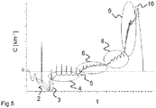
- Fig.5 shows the progression of the curvature C of the layered substrate over time t in the course of the deposition of the epi layer on the silicon substrate, wherein 0 denotes the borderline between concave (negative) and convex (positive) deformation.
- the dispersion performance of the AlGaN buffer was measured using the methodology as described by S. Stoffels et al. (The physical mechanism of dispersion caused by AlGaN/GaN buffers on Si and optimization for low dispersion, 2015 IEEE International Electron Devices Meeting (IEDM), 2015, p. 35.4.1-35.4.4 ).
- Metal pads 11 with a spacing of 10 ⁇ m have been deposited as shown in Fig.6 to measure the 2DEG (two-dimensional electron gas) resistance.
- a voltage of - 600 V (V stress ) was applied as electrical stress on the backside of Si substrate for 10 s (stress stage). Then the stress was removed and a sensing voltage of 1 V was applied over the 2DEG resistor (recovery stage).
- the switching delay between stress stage and recovery stage was 1 ms.
- the ratio of the initial 2DEG resistance of the unstressed device to the values measured after stress removal was nearly 1. Accordingly, there was no change in 2DEG conductivity and the AlGaN buffer induced dispersion was almost 0 %.
- a Van der Pauw hall measurement was carried on the device shown in Fig.6 at room temperature with the following results: sheet resistance 425 ⁇ /sq, carrier density 9.76 x 10 12 cm -2 and carrier mobility 1466 cm 2 /Vs.
- a further heteroepitaxial wafer was produced having the AlGaN buffer structure according to Fig.4 except of the third strain building layer 7, the AlGaN barrier layer 10a, the SiN passivation layer 10b and metal pads 11.
- the heteroepitaxial wafer had the following structure:
- the total thickness of the epi layer was 4.5 ⁇ m (200 nm AlN layer 2, 1800 nm layers 3, 4, 5 and 6, 1200 nm superlattice block 8, 1000 nm carbon doped GaN layer 9a, and 300 nm unintentionally doped GaN layer 9b.
- a heteroepitaxial wafer not representing the invention was grown which differed to the further heteroepitaxial wafer merely in regard of the first and second strain preserving blocks 4 and 6 which had been omitted.
- the thickness of the superlattice block 8 had been enlarged, respectively.
- the total thickness of the epi layer was also 4.5 ⁇ m (200 nm AlN layer 2, 100 nm AlGaN 3, 2900 nm superlattice block 8, 1000 nm carbon doped GaN layer 9a, and 300 nm unintentionally doped GaN layer 9b.
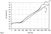
- Fig.7 displays breakdown curves obtained from the further heteroepitaxial wafer according to the invention and from the heteroepitaxial wafer used as a comparative example after the provision of 500 ⁇ m x 500 ⁇ m contact pads on top of the GaN layer and the bottom of the silicon substrate.
- the curves displayed represent the vertical leakage current vlc over the vertical bias voltage vbv.
- the upper curves (uc) were obtained from the further heteroepitaxial wafer, whereas the lower curves (Ic) were obtained from the heteroepitaxial wafer used as comparative example.
- the leakage current obtained from the further heteroepitaxial wafer was almost an order less than the leakage current obtained from the heteroepitaxial wafer used as a comparative example.
- the further heteroepitaxial wafer suffered a hard breakdown of the AlGaN buffer not up to 1500 V.
Landscapes
- Junction Field-Effect Transistors (AREA)
- Chemical & Material Sciences (AREA)
- Crystallography & Structural Chemistry (AREA)
- Crystals, And After-Treatments Of Crystals (AREA)
Abstract
Description
- The invention relates to a heteroepitaxial wafer comprising in the following order a silicon substrate, an AIN nucleation layer, an AlGaN buffer and a GaN layer. The invention further relates to a method for producing such heteroepitaxial wafer.
- Lattice mismatch between the substrate and the layers deposited thereon and differences regarding their thermal coefficient of expansion will lead to warping of the multi-layer structure during growth of the layers and during cooling down of the layered substrate to room temperature. Warping of the wafer may induce the formation of cracks.
-
US 2014/0374771 A1 discloses a semiconductor multi-layer substrate, a semiconductor device and a method for manufacturing the same. The multi-layer substrate comprises a substrate made of silicon, a first warp control layer giving a predetermined warp to the substrate and a second warp control layer. An amount of increase in warp per unit thickness of the second warp control layer is smaller than an amount of increase in warp per unit thickness of the first warp control layer. An effect is obtained, namely that a current leakage and a current collapse can be restrained without increasing a crack density and that production costs can be reduced. - Rowena et al. report that increasing the thickness of the buffer tends to suppress vertical leakage current and improves the breakdown performance of AlGaN/GaN high-electon-mobility (HEMT) devices ("Buffer Thickness Contribution to Suppress Vertical Leakage Current With High Breakdown Field (2.3 MV/cm) for GaN on Si" IEEE Electron Device Letters, VOL. 32, NO. 11, November 2011).
- It is also known that the curvature increases when the thickness of the substrate decreases, and it was concluded accordingly that the growth of GaN on 150 mm and 200 mm substrates requires much larger compressive strain in the epitaxial films (Y.Cao et al., "GaN-on-Silicon Growth by MOCVD: A Mechanistic Approach to Wafer Scaling"; CS MANTECH Conference, May 19th-22nd, 2014, Colorado, USA).
- The inventors of the present invention found that there is still the need to solve various problems.
If the thickness of the AlGaN buffer is increased in order to improve the breakdown characteristics, wafer warp will increase, as well, all the more as when silicon substrates having comparatively large diameters of 150 mm or 200 mm or 300 mm and having thicknesses in accordance with the SEMI standard are used.
Large wafer warp during epi deposition causes temperature non-uniformity on the surface that ultimately results in layer thickness variation and material alloy fluctuation across the wafer diameter. - The present invention was made in order to address these problems.
- The present invention is directed to a heteroepitaxial wafer comprising in the following order
a silicon substrate having a diameter and a thickness;
an AIN nucleation layer;
a first strain building layer which is an AlzGa1-zN layer having a first average Al content z, wherein 0 < z;
a first strain preserving block comprising not less than 5 and not more than 50 units of a first sequence of layers, the first sequence of layers comprising an AIN layer and at least two AlGaN layers, the first strain preserving block having a second average Al content y, wherein y > z;
a second strain building layer which is an AlxGa1-xN layer having a third average Al content x, wherein 0 ≤ x < y;
a second strain preserving block comprising not less than 5 and not more than 50 units of a second sequence of layers, the second sequence of layers comprising an AIN layer and at least one AlGaN layer, the second strain preserving block having a fourth average Al content w, wherein x < w < y, and
a GaN layer, wherein the layers between the AIN nucleation layer and the GaN layer form an AlGaN buffer. - The present invention is further directed to a method for producing a heteroepitaxial wafer, the method comprising steps in the following order:
- providing a silicon substrate having a diameter and a thickness, and depositing a multiplicity of layers on the silicon substrate thereby forming a layered substrate, comprising
- depositing on the silicon substrate an AIN nucleation layer;
- depositing on the AIN nucleation layer a first strain building layer which is an AlzGa1-zN layer having a first average Al content z, wherein 0 < z;
- depositing on the first strain building layer a first strain preserving block comprising not less than 5 and not more than 50 units of a first sequence of layers, the first sequence of layers comprising an AIN layer and at least two AlGaN layers, the first strain preserving block having a second average Al content y, wherein y > z;
- depositing on the first strain preserving block a second strain building layer which is an AlxGa1-xN layer having a third average Al content x, wherein 0 ≤ x < y;
- depositing on the second strain building layer a second strain preserving block comprising not less than 5 and not more than 50 units of a second sequence of layers, the second sequence of layers comprising an AIN layer and at least one AlGaN layer, the second strain preserving block having a fourth average Al content w, wherein x < w < y; and
- depositing on the second strain preserving block a GaN layer.
- Preferably, the mentioned nitride containing layers are deposited by metalorganic chemical vapor deposition (MOCVD). As precursor compounds trimethylgallium, trimethylaluminum and ammonia can be used. Hydrogen or nitrogen is a suitable carrier gas. The growth temperature of the nitride containing layers is preferably not less than 700 °C and not more than 1160 °C.
- The silicon substrate is preferably a silicon single crystal wafer having a diameter of 150 mm and a thickness of not more than 1000 µm, preferably not more than 675 µm, or having a diameter of 200 mm and a thickness of not more than 1200 µm, preferably not more than 725 µm, or having a diameter of 300 mm and a thickness of not more than 1500 µm, preferably not more than 775 µm. Preferably, the silicon substrate has {111}-orientation and a crystal offcut of less than or equal to 2°. Alternatively, the silicon substrate can have the mentioned orientation and offcut and be an SOI wafer (silicon-on-insulator wafer) or a layered wafer having a silicon single crystal top layer.
- The AIN nucleation layer has a thickness which is preferably not less than 100 nm and not more than 300 nm. The curvature of the substrate becomes more negative, i.e. more concave with increasing thickness of the AIN nucleation layer.
- The first strain building layer is an AlGaN layer having a first average Al content z, i.e. the first strain building layer is an AlzGa1-zN layer, wherein 0 < z. Alternatively, the first strain building layer can comprise more than one AlGaN layer with decreasing Al content in growth direction. Preferably, the value of z is not less than 40 % and not more than 60 %. The first strain building layer forms an interface with the top surface of the AIN nucleation layer. The first strain building layer reduces the concave curvature so that the layered substrate becomes less concave under the conditions of growth of the first strain building layer. The concave curvature decreases the more the thinner the substrate is. Preferably, the curvature of the layered substrate remains concave in the course of growth of the first strain building layer. The thickness of the first strain building layer is preferably not less than 30 nm and not more than 200 nm.
- The first strain preserving block comprises not less than 5 and not more than 50 units of a first sequence of layers. The first sequence of layers comprises an AIN layer and at least two AlGaN layers differing in regard of their Al content. Preferably, the Al content of the top surface of the first strain building layer is equal to or more than the Al content of the closest AlGaN layer of the first strain preserving block. Moreover, it is preferable that the AIN layer of the first unit forms an interface with the top surface of the first strain building layer. The Al content decreases in the first sequence of layers with increasing distance from the substrate. Preferably, one AlGaN layer of the first sequence of layers is a graded composition AlGaN layer. The grading of the Al composition can be stepwise or continuous.
- According to a preferred embodiment of the invention, the first sequence of layers in growth direction consists of an AIN layer, a thick constant composition AlGaN layer, a continuously graded composition AlGaN layer, and, optionally, a thin constant composition AlGaN layer. The thickness of the thick constant composition AlGaN layer is at least twice the thickness of the continuously graded composition AlGaN layer and at least twice the thickness of the thin constant composition AlGaN layer. The Al content of the thin constant composition AlGaN layer is equal to or similar to the Al content of the top surface of the continuously graded AlGaN layer. The curvature of the layered substrate more rapidly increases during the growth of the continuously graded composition AlGaN layer than during the growth of the thick and thin constant composition layers. The curvature of the layered substrate can be readily controlled just by adapting the Al content and the thickness of the continuously graded composition AlGaN layer.
- The first strain preserving block has a second average Al content which is y, wherein y > z. Preferably, the first strain preserving block is deposited until the curvature of the layered substrate becomes zero, or until the curvature of the layered substrate becomes less concave than at the beginning of the deposition of the first strain preserving block. While depositing the first strain preserving block, the change in curvature ΔC with respect to the change of the thickness Δth of the first strain preserving block (ΔC/Δth) preferably becomes positive in the beginning of the deposition and then becomes almost 'zero', i.e. remains almost constant or constant or even becomes negative. The thickness of the strain preserving block does not much influence the curvature of the layered substrate. Preferably, the growth of the first strain preserving block is stopped when the value of ΔC/Δth becomes less than -5 km-1/µm.
- The second strain building layer is an AlGaN layer having a third average Al content x, i.e. the second strain building layer is an AlxGa1-xN layer, wherein 0 ≤ x < y. It is preferable that the second strain building layer forms an interface with the top surface of the first strain preserving block, wherein the third average Al content is less than the Al content of the top surface of the first strain preserving block. The second strain building layer builds compressive strain, and the thickness and the Al content of the second strain building layer are chosen such that the curvature of the layered substrate becomes close to zero, i.e. preferably less than |3| km-1 at the end of the deposition of the second strain building layer. Then, the layered substrate is almost flat after the second strain building layer has been grown. The thickness of the second strain building layer is preferably not less than 30 nm and not more than 200 nm.
- The second strain preserving block comprises not less than 5 and not more than 50 units of a second sequence of layers. The second sequence of layers comprises an AIN layer and at least one AlGaN layer. It is preferable that the AIN layer of the first unit forms an interface with the top surface of the second strain building layer. The AlGaN layer of the second sequence of layers can be a constant composition AlGaN layer or a graded composition AlGaN layer, the Al decreasing with increasing distance from the substrate. The grading of the Al composition can be stepwise or continuous. According to a preferred embodiment of the invention, the AlGaN layer of the second sequence of layers is a constant composition AlGaN layer and its Al content is equal to or less than x. The second strain preserving block has a fourth average Al content which is w, wherein x < w < y.
- Preferably, the second strain preserving block is deposited until the difference in curvature of the layered substrate to the beginning of the deposition of the second strain preserving block becomes negative.
- The second strain preserving block does not substantially alter the curvature of the layered substrate. Preferably, the growth of the second strain preserving block is stopped when the value of ΔC/Δth is less than -1 km-1/µm, and the layered substrate stays almost flat after the second strain preserving block has been grown.
- The GaN layer forms an interface with the top surface of the second strain preserving block or, alternatively, the GaN layer forms an interface with the top surface of an optional third strain building layer or, alternatively, the GaN layer forms an interface with the top surface of an optional superlattice block.
- If present, the third strain building layer is an AlGaN layer having a fifth average Al content v, i.e. the third strain building layer is an AlvGa1-vN layer, wherein 0 ≤ v < w. The third strain building layer forms an interface with the top surface of the second strain preserving block, wherein the fifth average Al content is preferably less than the Al content of the top surface of the second strain preserving block. The third strain building layer further builds up compressive strain and further increases the convex curvature of the layered substrate. The thickness of the second strain building layer is preferably not less than 30 nm and not more than 200 nm.
- The implementation of strain building layers alternating with strain preserving blocks results in the provision of a comparatively thick AlGaN buffer while keeping the layered substrate almost flat, the wafer curvature not exceeding 25 km-1 and without plastic deformation occurring.
- In case that the superlattice block is present, the superlattice block forms an interface with either the top surface of the second strain preserving block (i.e. the third strain building layer is not present) or with the top surface of the third strain building layer.
- The superlattice block preferably comprises not less than 10 and not more than 100 layer units, each comprising an AIN layer and an AlGaN layer. The AIN layer of the first unit of the superlattice block forms an interface with either the top surface of the second strain preserving block (i.e. the third strain building layer is not present) or with the top surface of the third strain building layer. The AIN layer of the unit of the superlattice block has a thickness which is preferably not less than 5 nm and not more than 10 nm. The AlGaN layer of the unit of the superlattice block has a thickness which is preferably 2 to 10 times the thickness of the AIN layer of the unit of the superlattice block. The AlGaN layer of the unit of the superlattice block has a content of Al which is equal to or less than the Al content of the AlGaN layer which is next underneath the superlattice block. The superlattice block has a sixth average Al content which is u, wherein v < u < w. The superlattice block allows moderately increasing the convex curvature of the layered substrate.
- Regardless whether the third strain building layer and/or the superlattice block is present or not, the AlGaN buffer has an average Al content which is preferably not less than 30 %. Moreover, the AlGaN buffer has a thickness which is preferably not less than 1.0 µm and not more than 5 µm.
- The GaN layer can be a high purity GaN layer which is not intentionally doped and has a carbon concentration which is preferably less than 1 x 10¹⁸ atoms/cm3 and has a thickness which is preferably not less than 50 nm and not more than 500 nm.
- Preferably, the GaN layer comprises an insulating GaN buffer containing carbon and the high purity GaN layer. In case that the insulating GaN buffer is present, the high purity GaN layer forms an interface with the insulating GaN buffer, and the insulating GaN buffer forms an interface with the second strain preserving block or the third strain building layer or the superlattice block.
- The concentration of carbon in the insulating GaN buffer is preferably not less than 1 x 10¹⁸ atoms/cm3 and not more than 1 x 10²⁰ atoms/cm3. The insulating GaN buffer has a thickness which is preferably not less than 500 nm and not more than 2000 nm.
- The deposition of the GaN layer is preferably started at a point in time, when the curvature of the layered substrate is convex and not more than 50 km-1.
- Regardless whether the insulating GaN buffer is present or not, the top surface of the GaN layer has a root mean square (RMS) roughness which is preferably less than 0.5 nm on 5 µm x 5 µm atomic force microscope (AFM) scan area, and the full width at half maximum (FWHM) of X-ray diffraction (XRD) rocking curve for 002 and 102 reflections of the GaN layer is preferably less than 650 arcsec and 1200 arcsec, respectively.
- The heteroepitaxial wafer according to the invention has excellent material properties regarding warp. For example, with an epilayer having a thickness of 4.5 µm, the epilayer is crack-free (3 mm edge exclusion considered), and the warp of the heteroepitaxial wafer is less than | 50 | µm.
- Due to a high breakdown field which is more than 2.5 MV/cm for a vertical leakage current of 1 mA/mm2 on (111)-oriented silicon having a diameter of at least 150 mm, the heteroepitaxial wafer according to the invention can be used to build a 600 V HEMT (high electron mobility transistor) devices thereon.
- For this purpose, a device layer may be formed on top of the GaN layer. The device layer may comprise, for example, pGaN/AlGaN layers or SiN/AlGaN layers or SiN/AlGaN/AlN layers or GaN/AlGaN/AlN layers or GaN/AlGaN layers or an AlGaN layer.
- Layered substrate means the substrate and at least one layer deposited thereon. Epilayer means the total of the layers grown on the substrate.
AlGaN buffer means the total of layers situated above the AIN nucleation layer and below the GaN layer.
Heteroepitaxial wafer means the entity comprising the substrate, the AIN nucleation layer, the AlGaN buffer and the GaN layer.
The Al content or average Al content of a layer can be specified as percentage of Al atoms present relative of the total sum of group III atoms present.
Curvature means the reciprocal of a radius of curvature of the layered substrate or the heteroepitaxial wafer, respectively.
Warp means the difference between the maximum and minimum distances of the median surface of a wafer from a reference plane. - The invention is further explained with reference to drawings.
-
-
Fig.1 displays a curved silicon substrate under thermal conditions of the deposition of a group III-nitride layer. -
Fig.2 schematically displays a first sequence of layers of a first strain preserving block according to a preferred embodiment of the invention. -
Fig.3 qualitatively shows how curvature C of the layered substrate and thickness th of the layers correlate during the growth of the first sequence of layers (solid line) whichFig.2 refers to. -
Fig.4 schematically displays the structure of a heteroepitaxial wafer according to a preferred embodiment of the invention. -
Fig.5 shows the progression of the curvature C of the layered substrate over time t in the course of the deposition of an epi layer displayed inFig.4 . -
Fig.6 displays the structure of a device based on the heteroepitaxial wafer according toFig.4 and used for measuring the dispersion performance of the AlGaN buffer. -
Fig.7 displays breakdown curves obtained from a heteroepitaxial wafer according to the invention and from a heteroepitaxial wafer used as a comparative example. -
- 1 silicon substrate
- 2 AIN nucleation layer
- 3 first strain building layer
- 4 first strain preserving block
- 5 second strain building layer
- 6 second strain preserving block
- 7 third strain building layer
- 8 superlattice block
- 9 GaN layer
- 9a carbon doped GaN layer
- 9b unintentionally doped GaN layer
- 10 device layer
- 10a AlGaN barrier layer
- 10b SiN passivation layer
- 11 metal pad
- 20 AIN layer
- 30 constant composition AlGaN layer
- 40 continuously graded AlGaN layer
- 50 thin constant composition AlGaN layer
- The
silicon substrate 1 is heated from the backside (Fig.1 ). While heating, the temperature T1 at the top surface is less than temperature T2 at the bottom surface of thesilicon substrate 1. This negative temperature gradient ΔT (T1 - T2) results in a concave shape of thesubstrate 1, i.e. in negative substrate curvature prior to group-III nitride deposition, the negative curvature increasing with increasing substrate temperature. - Regardless whether the curvature is concave or convex, the temperature at the top surface varies along the radial position and the deposition conditions vary, as well. As a consequence, the material characteristics of a group-III nitride layer deposited on the top surface becomes radially inhomogeneous depending on the grade of curvature.
- The present invention avoids excessive curvature of the layered substrate resulting in homogeneous material characteristics of the layers and, at the same time, enables high breakdown field.
-
Fig.2 schematically displays a first sequence of layers of a first strain preserving block according to a preferred embodiment of the invention. The displayed first sequence of layers consists of anAlN layer 20, a thick constantcomposition AlGaN layer 30, a continuously gradedAlGaN layer 40 and a thin constantcomposition AlGaN layer 50. - Due to this structure, the second average Al content y of the first strain preserving block is dominated by the Al contents of the
AlN layer 20 and the thick constantcomposition AlGaN layer 30, and consequently, is comparatively high. This results in high breakdown field, helps reducing internal stress within the GaN layer and keeps the thermal expansion rate of the constantcomposition AlGaN layer 30 closer to that of the silicon substrate. -
Fig.3 qualitatively shows how curvature C of the layered substrate and thickness th of the layers correlate during the growth of the first sequence of layers (solid line) whichFig.2 refers to. For the purpose of comparison, the continuously gradedAlGaN layer 40 was omitted. Then, in order to obtain the same curvature of the layered substrate (dotted line), the Al content of thethick AlGaN layer 30 could be reduced or the thickness of theAlN layer 20 could be reduced. However, this would result in lowering the breakdown voltage of the AlGaN buffer and in increasing the leakage current. -
Fig.4 schematically displays the structure of a heteroepitaxial wafer according to a preferred embodiment of the invention which additionally comprises a device layer. The heteroepitaxial wafer accordingFig.4 consists of asilicon substrate 1, anAlN nucleation layer 2, a firststrain building layer 3, a firststrain preserving block 4, a secondstrain building layer 5, a secondstrain preserving block 6, a thirdstrain building layer 7, asuperlattice block 8, aGaN layer 9 and adevice layer 10. - A heteroepitaxial wafer according to
Fig.4 may have, for example, the following structure: - the
silicon substrate 1 is a (111)-oriented silicon single crystal wafer having a diameter of 150 mm and a thickness of 675 µm; - the
AIN nucleation layer 2 has a thickness of 200 nm; - the first
strain building layer 3 is an AlzGa1-zN layer having a thickness of i nm; - the first
strain preserving block 4 consists of 30 repeated units of the first sequence of layers, the layers of a unit having the following order with respect to increasing distance to the silicon substrate: an AIN layer having a thickness of j nm, an AlaGa1-aN layer having a thickness of k nm (where k > j), a continuously graded AlGaN layer having a thickness of l nm (where l < k) with an Al content decreasing from a % to b % and an AlbGa1-bN layer having a thickness of m nm (where m > l), the average Al content of a unit being y, where y > z; - the second
strain building layer 5 is an AlxGa1-xN (where x < y) layer having a thickness of n nm; - the second
strain preserving block 6 consists of 40 repeated units of the second sequence of layers, the layers of a unit having the following order with respect to increasing distance to the silicon substrate: an AIN layer having a thickness of j nm and an AlcGa1-cN (where c < b) layer having a thickness of p nm, the average Al content of a unit being w, where w > x and w < y; - the third
strain building layer 7 is an AlvGa1-vN (where v < w) layer having a thickness of q nm; - the
superlattice block 8 consists of 25 repeated units of layers, the layers of a unit having the following order with respect to increasing distance to the silicon substrate: an AlN layer having a thickness of j nm and an AldGa1-dN (where d < c) layer having a thickness of r nm, the average Al content of a unit being u, where u > v and u < w; - the
GaN layer 9 consists of a carbon dopedGaN layer 9a having a carbon concentration of 4 x 10¹⁹ atoms/cm3 and a thickness of 1000 nm and an unintentionally dopedGaN layer 9b having a thickness of 400 nm; and - the
device layer 10 consists of anAlGaN barrier layer 10a having an Al content of 25 % and a thickness of 25 nm and an in-situSiN passivation layer 10b. - In principle, a p-doped AlGaN (Al content ranging from 0 to 30%) can be deposited on top of the
AlGaN barrier layer 10a to fabricate e-mode HEMT devices. - A heteroepitaxial wafer with a structure according to
Fig.4 and having the above-mentioned composition was produced within a commercial MOCVD tool from Veeco Instruments, USA, in accordance with the invention, and the curvature of the layered substrate was monitored during the growth of the layers. -
Fig.5 shows the progression of the curvature C of the layered substrate over time t in the course of the deposition of the epi layer on the silicon substrate, wherein 0 denotes the borderline between concave (negative) and convex (positive) deformation. - The dispersion performance of the AlGaN buffer was measured using the methodology as described by S. Stoffels et al. (The physical mechanism of dispersion caused by AlGaN/GaN buffers on Si and optimization for low dispersion, 2015 IEEE International Electron Devices Meeting (IEDM), 2015, p. 35.4.1-35.4.4).
Metal pads 11 with a spacing of 10 µm have been deposited as shown inFig.6 to measure the 2DEG (two-dimensional electron gas) resistance. A voltage of - 600 V (Vstress) was applied as electrical stress on the backside of Si substrate for 10 s (stress stage). Then the stress was removed and a sensing voltage of 1 V was applied over the 2DEG resistor (recovery stage). The switching delay between stress stage and recovery stage was 1 ms. The ratio of the initial 2DEG resistance of the unstressed device to the values measured after stress removal was nearly 1. Accordingly, there was no change in 2DEG conductivity and the AlGaN buffer induced dispersion was almost 0 %. Moreover, a Van der Pauw hall measurement was carried on the device shown inFig.6 at room temperature with the following results: sheet resistance 425 Ω/sq, carrier density 9.76 x 1012 cm-2 and carrier mobility 1466 cm2/Vs. - Next, the breakdown performance was examined. For this purpose, a further heteroepitaxial wafer was produced having the AlGaN buffer structure according to
Fig.4 except of the thirdstrain building layer 7, theAlGaN barrier layer 10a, theSiN passivation layer 10b andmetal pads 11. - The heteroepitaxial wafer had the following structure:
- a (111)-oriented silicon single crystal wafer as
substrate 1 with a diameter of 150 mm and a thickness of 675 µm; - an
AIN nucleation layer 2 with a thickness of 200 nm; - a first
strain building layer 3, namely a AlzGa1-zN layer with a thickness of i nm; - a first
strain preserving block 4, namely 25 repeated units of the first sequence of layers, the layers of a unit with the following order with respect to increasing distance to the silicon substrate: an AIN layer with a thickness of j nm, an AlaGa1-aN layer with a thickness of k nm, a continuously graded AlGaN layer with a thickness of l nm and with an Al content decreasing from a % to b %, and an AlbGa1-bN layer with a thickness of m nm; - a second
strain building layer 5, namely an AlxGa1-xN layer with a thickness of n nm; - a second
strain preserving block 6, namely 36 repeated units of the second sequence layers, the layers of a unit with the following order with respect to increasing distance to the silicon substrate: an AIN layer with a thickness of j nm and an AlcGa1-cN layer with a thickness of p nm; - a
superlattice block 8 with 41 repeated units of layers, the layers of a unit with the following order with respect to increasing distance to the silicon substrate: an AIN layer with a thickness of j nm and an AldGa1-dN layer with a thickness of r nm; - a carbon doped
GaN layer 9a with a carbon concentration of 4 x 10¹⁹ atoms/cm3 and a thickness of 1000 nm; and - an unintentionally doped
GaN layer 9b with a thickness of 300 nm. - The total thickness of the epi layer was 4.5 µm (200
nm AlN layer 2, 1800nm layers nm superlattice block 8, 1000 nm carbon dopedGaN layer GaN layer 9b. - For the purpose of comparison, a heteroepitaxial wafer not representing the invention was grown which differed to the further heteroepitaxial wafer merely in regard of the first and second strain preserving blocks 4 and 6 which had been omitted. To compensate for the first and second strain preserving blocks 4 and 6, the thickness of the
superlattice block 8 had been enlarged, respectively. The total thickness of the epi layer was also 4.5 µm (200nm AlN layer 2, 100nm AlGaN 3, 2900nm superlattice block 8, 1000 nm carbon dopedGaN layer GaN layer 9b. -
Fig.7 displays breakdown curves obtained from the further heteroepitaxial wafer according to the invention and from the heteroepitaxial wafer used as a comparative example after the provision of 500 µm x 500 µm contact pads on top of the GaN layer and the bottom of the silicon substrate. The curves displayed represent the vertical leakage current vlc over the vertical bias voltage vbv. The upper curves (uc) were obtained from the further heteroepitaxial wafer, whereas the lower curves (Ic) were obtained from the heteroepitaxial wafer used as comparative example. - At 600 V bias, the leakage current obtained from the further heteroepitaxial wafer was almost an order less than the leakage current obtained from the heteroepitaxial wafer used as a comparative example. The further heteroepitaxial wafer suffered a hard breakdown of the AlGaN buffer not up to 1500 V.
Claims (14)
- A heteroepitaxial wafer comprising in the following order
a silicon substrate having a diameter and a thickness;
an AIN nucleation layer;
a first strain building layer which is an AlzGa1-zN layer having a first average Al content z, wherein 0 < z;
a first strain preserving block comprising not less than 5 and not more than 50 units of a first sequence of layers, the first sequence of layers comprising an AIN layer and at least two AlGaN layers, the first strain preserving block having a second average Al content y, wherein y > z;
a second strain building layer which is an AlxGa1-xN layer having a third average Al content x, wherein 0 ≤ x < y;
a second strain preserving block comprising not less than 5 and not more than 50 units of a second sequence of layers, the second sequence of layers comprising an AlN layer and at least one AlGaN layer, the second strain preserving block having a fourth average Al content w, wherein x < w < y, and
a GaN layer, wherein the layers between the AlN nucleation layer and the GaN layer form an AlGaN buffer. - A heteroepitaxial wafer according to claim 1, wherein the AlGaN buffer has a thickness of not less than 1.0 µm and not more than 5 µm.
- A heteroepitaxial wafer according to claim 1 or claim 2, wherein the AlGaN buffer has an average Al content of not less than 30 %.
- A heteroepitaxial wafer according to any one of claims 1 to 3, wherein the AlGaN buffer further comprises a third a strain building layer which is an AlvGa1-vN layer having a fifth average Al content v, wherein 0 ≤ v < w.
- A heteroepitaxial wafer according to any one of claims 1 to 4, wherein the AlGaN buffer further comprises a superlattice block, the superlattice block having a sixth average Al content u, wherein u > v and u < w.
- A heteroepitaxial wafer according to any one of claims 1 to 5, wherein the diameter and the thickness of the substrate is 150 mm and not more than 1000 µm, respectively, or 200 mm and not more than 1200 µm, respectively, or 300 mm and not more than 1500 µm, respectively.
- A heteroepitaxial wafer according to any of claims 1 to 6, wherein the AlGaN buffer has a breakdown strength of not less than 2.5 MV/cm.
- A heteroepitaxial wafer according to any of claims 1 to 7, wherein the silicon substrate is a silicon single crystal wafer, an SOI wafer or a layered wafer having a silicon single crystal top layer.
- A method for producing a heteroepitaxial wafer, the method comprising steps in the following order:providing a silicon substrate having a diameter and a thickness, and depositing a multiplicity of layers on the silicon substrate, thereby forming a layered substrate, comprisingdepositing on the silicon substrate an AlN nucleation layer;depositing on the AlN nucleation layer a first strain building layer which is an AlzGa1-zN layer having a first average Al content z, wherein 0 < z;depositing on the first strain building layer a first strain preserving block comprising not less than 5 and not more than 50 units of a first sequence of layers, the first sequence layers comprising an AlN layer and at least two AlGaN layers, the first strain preserving block having a second average Al content y, wherein y > z;depositing on the first strain preserving block a second strain building layer which is an AlxGa1-xN layer having a third average Al content x, wherein 0 ≤ x < y;depositing on the second strain building layer a second strain preserving block comprising not less than 5 and not more than 50 units of a second sequence of layers, the second sequence of layers comprising an AlN layer and at least one AlGaN layer, the second strain preserving block having a fourth average Al content w, wherein x < w < y; anddepositing on the second strain preserving block a GaN layer.
- A method according to claim 9, comprising performing the step of depositing the first strain preserving block at a point in time, when the curvature of the layered substrate is concave, and performing the step of depositing the second strain preserving block at a point in time, when the curvature of the layered substrate is convex.
- A method according to claim 9 or claim 10, comprising increasing the curvature of the layered substrate during the deposition of the first strain preserving block and stopping the growth of the first strain preserving block when the value of ΔC/Δth becomes less than -5 km-1/µm, wherein ΔC/Δth denotes the change of curvature ΔC with change of thickness Δth.
- A method according to any of claims 9 to 11, comprising stopping the growth of the second strain preserving block when the value of ΔC/Δt becomes less than -1 km-1/µm, wherein ΔC/Δth denotes the change of curvature ΔC with change of thickness Δth.
- A method according to any of claims 9 to 12, comprising starting the deposition of the GaN layer at a point in time, when the curvature of the layered substrate is convex and not more than 50 km-1.
- A method according to any of claims 9 to 13, wherein the provided silicon substrate has a diameter of 150 mm and a thickness of not more than 1000 µm, respectively, or a diameter of 200 mm and a thickness of not more than 1200 µm, respectively, or a diameter of 300 mm and a thickness of not more than 1500 µm, respectively.
Priority Applications (9)
| Application Number | Priority Date | Filing Date | Title |
|---|---|---|---|
| EP17188124.6A EP3451364B1 (en) | 2017-08-28 | 2017-08-28 | Heteroepitaxial wafer and method for producing a heteroepitaxial wafer |
| SG11202001447TA SG11202001447TA (en) | 2017-08-28 | 2018-08-16 | Heteroepitaxial wafer and method for producing a heteroepitaxial wafer |
| CN201880057884.0A CN111052307B (en) | 2017-08-28 | 2018-08-16 | Heteroepitaxial wafers and methods for manufacturing heteroepitaxial wafers |
| US16/643,003 US11869942B2 (en) | 2017-08-28 | 2018-08-16 | Heteroepitaxial wafer and method for producing a heteroepitaxial wafer |
| PCT/EP2018/072229 WO2019042782A1 (en) | 2017-08-28 | 2018-08-16 | Heteroepitaxial wafer and method for producing a heteroepitaxial wafer |
| KR1020207008513A KR102321952B1 (en) | 2017-08-28 | 2018-08-16 | Heteroepitaxial Wafer and Method of Manufacturing Heteroepitaxial Wafer |
| JP2020512014A JP6995979B2 (en) | 2017-08-28 | 2018-08-16 | Heteroepitaxial wafer and manufacturing method of heteroepitaxial wafer |
| MYPI2020000671A MY204823A (en) | 2017-08-28 | 2018-08-16 | Heteroepitaxial wafer and method for producing a heteroepitaxial wafer |
| TW107128973A TWI678727B (en) | 2017-08-28 | 2018-08-20 | Heteroepitaxial wafer and method for producing a heteroepitaxial wafer |
Applications Claiming Priority (1)
| Application Number | Priority Date | Filing Date | Title |
|---|---|---|---|
| EP17188124.6A EP3451364B1 (en) | 2017-08-28 | 2017-08-28 | Heteroepitaxial wafer and method for producing a heteroepitaxial wafer |
Publications (2)
| Publication Number | Publication Date |
|---|---|
| EP3451364A1 true EP3451364A1 (en) | 2019-03-06 |
| EP3451364B1 EP3451364B1 (en) | 2020-02-26 |
Family
ID=59738209
Family Applications (1)
| Application Number | Title | Priority Date | Filing Date |
|---|---|---|---|
| EP17188124.6A Active EP3451364B1 (en) | 2017-08-28 | 2017-08-28 | Heteroepitaxial wafer and method for producing a heteroepitaxial wafer |
Country Status (9)
| Country | Link |
|---|---|
| US (1) | US11869942B2 (en) |
| EP (1) | EP3451364B1 (en) |
| JP (1) | JP6995979B2 (en) |
| KR (1) | KR102321952B1 (en) |
| CN (1) | CN111052307B (en) |
| MY (1) | MY204823A (en) |
| SG (1) | SG11202001447TA (en) |
| TW (1) | TWI678727B (en) |
| WO (1) | WO2019042782A1 (en) |
Cited By (1)
| Publication number | Priority date | Publication date | Assignee | Title |
|---|---|---|---|---|
| CN112242435A (en) * | 2019-07-19 | 2021-01-19 | 环球晶圆股份有限公司 | Semiconductor epitaxial structure and forming method thereof |
Families Citing this family (13)
| Publication number | Priority date | Publication date | Assignee | Title |
|---|---|---|---|---|
| US12317532B2 (en) | 2021-04-12 | 2025-05-27 | Innoscience (Suzhou) Technology Co., Ltd. | Semiconductor device and method for manufacturing the same |
| US12274082B2 (en) | 2021-04-12 | 2025-04-08 | Innoscience (Suzhou) Technology Co., Ltd. | Semiconductor device and method for manufacturing the same |
| US12279444B2 (en) | 2021-04-12 | 2025-04-15 | Innoscience (Suzhou) Technology Co., Ltd. | Semiconductor device and method for manufacturing the same |
| US12125801B2 (en) | 2021-04-12 | 2024-10-22 | Innoscience (Suzhou) Technology Co., Ltd. | Semiconductor device and method for manufacturing the same |
| CN117203775A (en) | 2021-04-12 | 2023-12-08 | 英诺赛科(苏州)半导体有限公司 | Semiconductor device and manufacturing method thereof |
| US20220328678A1 (en) * | 2021-04-12 | 2022-10-13 | Innoscience (Suzhou) Technology Co., Ltd. | Semiconductor device and method for manufacturing the same |
| US12125902B2 (en) | 2021-04-12 | 2024-10-22 | Innoscience (Suzhou) Technology Co., Ltd. | Semiconductor device and method for manufacturing the same |
| US12289901B2 (en) | 2021-04-12 | 2025-04-29 | Innoscience (Suzhou) Technology Co., Ltd. | Semiconductor device and method for manufacturing the same |
| US12520548B2 (en) | 2021-10-27 | 2026-01-06 | Industrial Technology Research Institute | Semiconductor substrate with balanced stress |
| JP7378562B2 (en) * | 2021-10-27 | 2023-11-13 | 財團法人工業技術研究院 | Semiconductor substrate with equilibrium stress |
| TWI910573B (en) * | 2023-03-07 | 2026-01-01 | 環球晶圓股份有限公司 | Epitaxial structure |
| EP4539100A1 (en) * | 2023-10-12 | 2025-04-16 | Siltronic AG | Semiconductor wafer having a multilayered structure and method for producing the same |
| EP4760775A1 (en) | 2024-12-11 | 2026-06-17 | Siltronic AG | Wafer comprising a multilayered structure and method of producing a wafer comprising a multilayered structure |
Citations (5)
| Publication number | Priority date | Publication date | Assignee | Title |
|---|---|---|---|---|
| US20110272665A1 (en) * | 2010-05-07 | 2011-11-10 | Rohm Co., Ltd. | Nitride semiconductor device |
| US20120161152A1 (en) * | 2010-02-16 | 2012-06-28 | Ngk Insulators, Ltd. | Epitaxial substrate and method for manufacturing epitaxial substrate |
| US20130092953A1 (en) * | 2010-06-08 | 2013-04-18 | Ngk Insulators, Ltd. | Epitaxial substrate and method for manufacturing epitaxial substrate |
| US20140374771A1 (en) | 2012-03-16 | 2014-12-25 | Furukawa Electric Co., Ltd. | Semiconductor multi-layer substrate, semiconductor device, and method for manufacturing the same |
| EP2819152A1 (en) * | 2012-02-23 | 2014-12-31 | NGK Insulators, Ltd. | Semiconductor element and method for manufacturing semiconductor element |
Family Cites Families (32)
| Publication number | Priority date | Publication date | Assignee | Title |
|---|---|---|---|---|
| US7115896B2 (en) * | 2002-12-04 | 2006-10-03 | Emcore Corporation | Semiconductor structures for gallium nitride-based devices |
| US7910937B2 (en) * | 2005-02-02 | 2011-03-22 | Agency For Science, Technology And Research | Method and structure for fabricating III-V nitride layers on silicon substrates |
| EP2112699B1 (en) * | 2006-02-23 | 2020-05-06 | ALLOS Semiconductors GmbH | Nitride-based semiconductor product and method for its production |
| US20080054248A1 (en) * | 2006-09-06 | 2008-03-06 | Chua Christopher L | Variable period variable composition supperlattice and devices including same |
| JP5309452B2 (en) | 2007-02-28 | 2013-10-09 | サンケン電気株式会社 | Semiconductor wafer, semiconductor device, and manufacturing method |
| JP5477685B2 (en) * | 2009-03-19 | 2014-04-23 | サンケン電気株式会社 | Semiconductor wafer, semiconductor element and manufacturing method thereof |
| JP5634681B2 (en) * | 2009-03-26 | 2014-12-03 | 住友電工デバイス・イノベーション株式会社 | Semiconductor element |
| JP5572976B2 (en) * | 2009-03-26 | 2014-08-20 | サンケン電気株式会社 | Semiconductor device |
| JP5456783B2 (en) * | 2009-08-07 | 2014-04-02 | 日本碍子株式会社 | Epitaxial substrate for semiconductor element, method for manufacturing epitaxial substrate for semiconductor element, and semiconductor element |
| WO2011055543A1 (en) * | 2009-11-04 | 2011-05-12 | Dowaエレクトロニクス株式会社 | Epitaxially laminated iii-nitride substrate |
| JP6018360B2 (en) * | 2010-12-02 | 2016-11-02 | 富士通株式会社 | Compound semiconductor device and manufacturing method thereof |
| JP5662184B2 (en) | 2011-02-01 | 2015-01-28 | 日本碍子株式会社 | Epitaxial substrate for semiconductor device and method for manufacturing epitaxial substrate for semiconductor device |
| FR2977260B1 (en) * | 2011-06-30 | 2013-07-19 | Soitec Silicon On Insulator | PROCESS FOR PRODUCING A THICK EPITAXIAL LAYER OF GALLIUM NITRIDE ON A SILICON SUBSTRATE OR THE LIKE AND LAYER OBTAINED BY SAID METHOD |
| JP5665676B2 (en) * | 2011-07-11 | 2015-02-04 | Dowaエレクトロニクス株式会社 | Group III nitride epitaxial substrate and manufacturing method thereof |
| KR101813717B1 (en) * | 2012-01-04 | 2017-12-29 | 삼성전자주식회사 | Nitride semiconductor light emitting device |
| US8742396B2 (en) * | 2012-01-13 | 2014-06-03 | Dowa Electronics Materials Co., Ltd. | III nitride epitaxial substrate and deep ultraviolet light emitting device using the same |
| US8946773B2 (en) * | 2012-08-09 | 2015-02-03 | Samsung Electronics Co., Ltd. | Multi-layer semiconductor buffer structure, semiconductor device and method of manufacturing the semiconductor device using the multi-layer semiconductor buffer structure |
| JP5892014B2 (en) | 2012-09-14 | 2016-03-23 | 沖電気工業株式会社 | Nitride semiconductor device and method for identifying manufacturing conditions thereof |
| JP5425284B1 (en) * | 2012-09-21 | 2014-02-26 | 株式会社東芝 | Semiconductor wafer, semiconductor device, and method for manufacturing nitride semiconductor layer |
| US10256368B2 (en) * | 2012-12-18 | 2019-04-09 | Sk Siltron Co., Ltd. | Semiconductor substrate for controlling a strain |
| US8981382B2 (en) * | 2013-03-06 | 2015-03-17 | Iqe Rf, Llc | Semiconductor structure including buffer with strain compensation layers |
| JP6126906B2 (en) | 2013-05-14 | 2017-05-10 | シャープ株式会社 | Nitride semiconductor epitaxial wafer |
| JP6121806B2 (en) * | 2013-06-07 | 2017-04-26 | 株式会社東芝 | Nitride semiconductor wafer, nitride semiconductor device, and method of manufacturing nitride semiconductor wafer |
| JP6270536B2 (en) * | 2013-06-27 | 2018-01-31 | 株式会社東芝 | Nitride semiconductor device, nitride semiconductor wafer, and method of forming nitride semiconductor layer |
| KR102188493B1 (en) * | 2014-04-25 | 2020-12-09 | 삼성전자주식회사 | Method of growing nitride single crystal and method of manufacturing nitride semiconductor device |
| US9112077B1 (en) * | 2014-04-28 | 2015-08-18 | Industrial Technology Research Institute | Semiconductor structure |
| JP6180401B2 (en) | 2014-11-25 | 2017-08-16 | サンケン電気株式会社 | Epitaxial wafer, semiconductor element, epitaxial wafer manufacturing method, and semiconductor element manufacturing method |
| US9806183B2 (en) | 2015-11-30 | 2017-10-31 | Veeco Instruments, Inc. | Stress control on thin silicon substrates |
| WO2017145199A1 (en) * | 2016-02-26 | 2017-08-31 | サンケン電気株式会社 | Semiconductor base body and semiconductor device |
| CN106098749A (en) * | 2016-06-30 | 2016-11-09 | 中国电子科技集团公司第五十五研究所 | AlGaN/GaN heterojunction structure and growing method thereof on a kind of silicon substrate |
| US10211297B2 (en) * | 2017-05-03 | 2019-02-19 | Globalwafers Co., Ltd. | Semiconductor heterostructures and methods for forming same |
| TWI631668B (en) * | 2017-11-22 | 2018-08-01 | Elite Advanced Laser Corporation | Nitride semiconductor structure |
-
2017
- 2017-08-28 EP EP17188124.6A patent/EP3451364B1/en active Active
-
2018
- 2018-08-16 KR KR1020207008513A patent/KR102321952B1/en active Active
- 2018-08-16 SG SG11202001447TA patent/SG11202001447TA/en unknown
- 2018-08-16 JP JP2020512014A patent/JP6995979B2/en active Active
- 2018-08-16 MY MYPI2020000671A patent/MY204823A/en unknown
- 2018-08-16 WO PCT/EP2018/072229 patent/WO2019042782A1/en not_active Ceased
- 2018-08-16 CN CN201880057884.0A patent/CN111052307B/en active Active
- 2018-08-16 US US16/643,003 patent/US11869942B2/en active Active
- 2018-08-20 TW TW107128973A patent/TWI678727B/en active
Patent Citations (5)
| Publication number | Priority date | Publication date | Assignee | Title |
|---|---|---|---|---|
| US20120161152A1 (en) * | 2010-02-16 | 2012-06-28 | Ngk Insulators, Ltd. | Epitaxial substrate and method for manufacturing epitaxial substrate |
| US20110272665A1 (en) * | 2010-05-07 | 2011-11-10 | Rohm Co., Ltd. | Nitride semiconductor device |
| US20130092953A1 (en) * | 2010-06-08 | 2013-04-18 | Ngk Insulators, Ltd. | Epitaxial substrate and method for manufacturing epitaxial substrate |
| EP2819152A1 (en) * | 2012-02-23 | 2014-12-31 | NGK Insulators, Ltd. | Semiconductor element and method for manufacturing semiconductor element |
| US20140374771A1 (en) | 2012-03-16 | 2014-12-25 | Furukawa Electric Co., Ltd. | Semiconductor multi-layer substrate, semiconductor device, and method for manufacturing the same |
Non-Patent Citations (3)
| Title |
|---|
| "Buffer Thickness Contribution to Suppress Vertical Leakage Current With High Breakdown Field (2.3 MV/cm) for GaN on Si", IEEE ELECTRON DEVICE LETTERS, vol. 32, no. 11, November 2011 (2011-11-01) |
| S. STOFFELS ET AL.: "The physical mechanism of dispersion caused by AIGaN/GaN buffers on Si and optimization for low dispersion", 2015 IEEE INTERNATIONAL ELECTRON DEVICES MEETING (IEDM, 2015, pages 35.4.1 - 35.4.4 |
| Y.CAO ET AL.: "GaN-on-Silicon Growth by MOCVD: A Mechanistic Approach to Wafer Scaling", CS MANTECH CONFERENCE, 19 May 2014 (2014-05-19) |
Cited By (2)
| Publication number | Priority date | Publication date | Assignee | Title |
|---|---|---|---|---|
| CN112242435A (en) * | 2019-07-19 | 2021-01-19 | 环球晶圆股份有限公司 | Semiconductor epitaxial structure and forming method thereof |
| CN112242435B (en) * | 2019-07-19 | 2024-06-11 | 环球晶圆股份有限公司 | Semiconductor epitaxial structure and method for forming the same |
Also Published As
| Publication number | Publication date |
|---|---|
| SG11202001447TA (en) | 2020-03-30 |
| US11869942B2 (en) | 2024-01-09 |
| JP2020532139A (en) | 2020-11-05 |
| CN111052307A (en) | 2020-04-21 |
| US20200203485A1 (en) | 2020-06-25 |
| MY204823A (en) | 2024-09-18 |
| JP6995979B2 (en) | 2022-01-17 |
| KR20200039007A (en) | 2020-04-14 |
| WO2019042782A1 (en) | 2019-03-07 |
| TWI678727B (en) | 2019-12-01 |
| EP3451364B1 (en) | 2020-02-26 |
| TW201913740A (en) | 2019-04-01 |
| KR102321952B1 (en) | 2021-11-03 |
| CN111052307B (en) | 2023-10-03 |
Similar Documents
| Publication | Publication Date | Title |
|---|---|---|
| EP3451364B1 (en) | Heteroepitaxial wafer and method for producing a heteroepitaxial wafer | |
| CN103348447B (en) | Semiconductor wafers comprising gallium nitride with one or more interlayers of silicon nitride therein | |
| JP5188545B2 (en) | Compound semiconductor substrate | |
| US20070194342A1 (en) | GaN SEMICONDUCTOR DEVICE AND PROCESS EMPLOYING GaN ON THIN SAPHIRE LAYER ON POLYCRYSTALLINE SILICON CARBIDE | |
| KR102372451B1 (en) | Method for manufacturing compound semiconductor substrate and compound semiconductor substrate | |
| CN103782375A (en) | III nitride epitaxial substrate and method for manufacturing same | |
| JP5179635B1 (en) | Method for manufacturing substrate having buffer layer structure for growing nitride semiconductor layer | |
| TW202013433A (en) | A iii-n semiconductor structure and a method for forming a iii-n semiconductor structure | |
| KR20180014729A (en) | Stress Control for Heteroepitaxy | |
| US20160020346A1 (en) | Nitride semiconductor structure | |
| CN104126223A (en) | Semiconductor element and method for manufacturing semiconductor element | |
| WO2012071272A2 (en) | Layer structures for controlling stress of heteroepitaxially grown iii-nitride layers | |
| WO2006135477A1 (en) | Group iii nitride epitaxial layers on silicon carbide substrates | |
| CN109817698A (en) | The method for forming the semiconductor structure for gallium nitride channel device | |
| US20150357451A1 (en) | Semiconductor device for high-power applications | |
| JP2013145782A (en) | Epitaxial wafer for hetero-junction field effect transistor | |
| Hayashi et al. | Curvature-controllable and crack-free AlN/sapphire templates fabricated by sputtering and high-temperature annealing | |
| Gkanatsiou et al. | Influence of 4H-SiC substrate miscut on the epitaxy and microstructure of AlGaN/GaN heterostructures | |
| JP2011066333A (en) | Epitaxial substrate for electronic device and method of manufacturing the same, and epitaxial substrate for group iii nitride electronic device | |
| US20240363342A1 (en) | METHODS AND STRUCTURES FOR REDUCING DEFORMATIONS OF GALLIUM NITRIDE (GaN) DEVICES | |
| US20160118486A1 (en) | Semiconductor device | |
| CN118943007A (en) | Epitaxial wafer and preparation method thereof | |
| US20230178643A1 (en) | High electron mobility transistor device | |
| JP6527667B2 (en) | Method of manufacturing nitride semiconductor substrate | |
| Liu et al. | Effect of High Al Content AlGaN Buffer Layer on the Properties of GaN‐on‐Silicon Materials |
Legal Events
| Date | Code | Title | Description |
|---|---|---|---|
| PUAI | Public reference made under article 153(3) epc to a published international application that has entered the european phase |
Free format text: ORIGINAL CODE: 0009012 |
|
| STAA | Information on the status of an ep patent application or granted ep patent |
Free format text: STATUS: REQUEST FOR EXAMINATION WAS MADE |
|
| 17P | Request for examination filed |
Effective date: 20170911 |
|
| AK | Designated contracting states |
Kind code of ref document: A1 Designated state(s): AL AT BE BG CH CY CZ DE DK EE ES FI FR GB GR HR HU IE IS IT LI LT LU LV MC MK MT NL NO PL PT RO RS SE SI SK SM TR |
|
| AX | Request for extension of the european patent |
Extension state: BA ME |
|
| RIC1 | Information provided on ipc code assigned before grant |
Ipc: H01L 21/20 20060101AFI20190703BHEP |
|
| GRAP | Despatch of communication of intention to grant a patent |
Free format text: ORIGINAL CODE: EPIDOSNIGR1 |
|
| STAA | Information on the status of an ep patent application or granted ep patent |
Free format text: STATUS: GRANT OF PATENT IS INTENDED |
|
| RBV | Designated contracting states (corrected) |
Designated state(s): AL AT BE BG CH CY CZ DE DK EE ES FI FR GB GR HR HU IE IS IT LI LT LU LV MC MK MT NL NO PL PT RO RS SE SI SK SM TR |
|
| INTG | Intention to grant announced |
Effective date: 20191010 |
|
| GRAS | Grant fee paid |
Free format text: ORIGINAL CODE: EPIDOSNIGR3 |
|
| GRAA | (expected) grant |
Free format text: ORIGINAL CODE: 0009210 |
|
| STAA | Information on the status of an ep patent application or granted ep patent |
Free format text: STATUS: THE PATENT HAS BEEN GRANTED |
|
| AK | Designated contracting states |
Kind code of ref document: B1 Designated state(s): AL AT BE BG CH CY CZ DE DK EE ES FI FR GB GR HR HU IE IS IT LI LT LU LV MC MK MT NL NO PL PT RO RS SE SI SK SM TR |
|
| REG | Reference to a national code |
Ref country code: GB Ref legal event code: FG4D |
|
| REG | Reference to a national code |
Ref country code: CH Ref legal event code: EP |
|
| REG | Reference to a national code |
Ref country code: AT Ref legal event code: REF Ref document number: 1238662 Country of ref document: AT Kind code of ref document: T Effective date: 20200315 |
|
| REG | Reference to a national code |
Ref country code: IE Ref legal event code: FG4D |
|
| REG | Reference to a national code |
Ref country code: DE Ref legal event code: R096 Ref document number: 602017012171 Country of ref document: DE |
|
| PG25 | Lapsed in a contracting state [announced via postgrant information from national office to epo] |
Ref country code: FI Free format text: LAPSE BECAUSE OF FAILURE TO SUBMIT A TRANSLATION OF THE DESCRIPTION OR TO PAY THE FEE WITHIN THE PRESCRIBED TIME-LIMIT Effective date: 20200226 Ref country code: RS Free format text: LAPSE BECAUSE OF FAILURE TO SUBMIT A TRANSLATION OF THE DESCRIPTION OR TO PAY THE FEE WITHIN THE PRESCRIBED TIME-LIMIT Effective date: 20200226 Ref country code: NO Free format text: LAPSE BECAUSE OF FAILURE TO SUBMIT A TRANSLATION OF THE DESCRIPTION OR TO PAY THE FEE WITHIN THE PRESCRIBED TIME-LIMIT Effective date: 20200526 |
|
| REG | Reference to a national code |
Ref country code: NL Ref legal event code: MP Effective date: 20200226 |
|
| REG | Reference to a national code |
Ref country code: LT Ref legal event code: MG4D |
|
| PG25 | Lapsed in a contracting state [announced via postgrant information from national office to epo] |
Ref country code: BG Free format text: LAPSE BECAUSE OF FAILURE TO SUBMIT A TRANSLATION OF THE DESCRIPTION OR TO PAY THE FEE WITHIN THE PRESCRIBED TIME-LIMIT Effective date: 20200526 Ref country code: IS Free format text: LAPSE BECAUSE OF FAILURE TO SUBMIT A TRANSLATION OF THE DESCRIPTION OR TO PAY THE FEE WITHIN THE PRESCRIBED TIME-LIMIT Effective date: 20200626 Ref country code: LV Free format text: LAPSE BECAUSE OF FAILURE TO SUBMIT A TRANSLATION OF THE DESCRIPTION OR TO PAY THE FEE WITHIN THE PRESCRIBED TIME-LIMIT Effective date: 20200226 Ref country code: SE Free format text: LAPSE BECAUSE OF FAILURE TO SUBMIT A TRANSLATION OF THE DESCRIPTION OR TO PAY THE FEE WITHIN THE PRESCRIBED TIME-LIMIT Effective date: 20200226 Ref country code: HR Free format text: LAPSE BECAUSE OF FAILURE TO SUBMIT A TRANSLATION OF THE DESCRIPTION OR TO PAY THE FEE WITHIN THE PRESCRIBED TIME-LIMIT Effective date: 20200226 Ref country code: GR Free format text: LAPSE BECAUSE OF FAILURE TO SUBMIT A TRANSLATION OF THE DESCRIPTION OR TO PAY THE FEE WITHIN THE PRESCRIBED TIME-LIMIT Effective date: 20200527 |
|
| PG25 | Lapsed in a contracting state [announced via postgrant information from national office to epo] |
Ref country code: NL Free format text: LAPSE BECAUSE OF FAILURE TO SUBMIT A TRANSLATION OF THE DESCRIPTION OR TO PAY THE FEE WITHIN THE PRESCRIBED TIME-LIMIT Effective date: 20200226 |
|
| PG25 | Lapsed in a contracting state [announced via postgrant information from national office to epo] |
Ref country code: EE Free format text: LAPSE BECAUSE OF FAILURE TO SUBMIT A TRANSLATION OF THE DESCRIPTION OR TO PAY THE FEE WITHIN THE PRESCRIBED TIME-LIMIT Effective date: 20200226 Ref country code: SM Free format text: LAPSE BECAUSE OF FAILURE TO SUBMIT A TRANSLATION OF THE DESCRIPTION OR TO PAY THE FEE WITHIN THE PRESCRIBED TIME-LIMIT Effective date: 20200226 Ref country code: DK Free format text: LAPSE BECAUSE OF FAILURE TO SUBMIT A TRANSLATION OF THE DESCRIPTION OR TO PAY THE FEE WITHIN THE PRESCRIBED TIME-LIMIT Effective date: 20200226 Ref country code: SK Free format text: LAPSE BECAUSE OF FAILURE TO SUBMIT A TRANSLATION OF THE DESCRIPTION OR TO PAY THE FEE WITHIN THE PRESCRIBED TIME-LIMIT Effective date: 20200226 Ref country code: RO Free format text: LAPSE BECAUSE OF FAILURE TO SUBMIT A TRANSLATION OF THE DESCRIPTION OR TO PAY THE FEE WITHIN THE PRESCRIBED TIME-LIMIT Effective date: 20200226 Ref country code: LT Free format text: LAPSE BECAUSE OF FAILURE TO SUBMIT A TRANSLATION OF THE DESCRIPTION OR TO PAY THE FEE WITHIN THE PRESCRIBED TIME-LIMIT Effective date: 20200226 Ref country code: CZ Free format text: LAPSE BECAUSE OF FAILURE TO SUBMIT A TRANSLATION OF THE DESCRIPTION OR TO PAY THE FEE WITHIN THE PRESCRIBED TIME-LIMIT Effective date: 20200226 Ref country code: ES Free format text: LAPSE BECAUSE OF FAILURE TO SUBMIT A TRANSLATION OF THE DESCRIPTION OR TO PAY THE FEE WITHIN THE PRESCRIBED TIME-LIMIT Effective date: 20200226 Ref country code: PT Free format text: LAPSE BECAUSE OF FAILURE TO SUBMIT A TRANSLATION OF THE DESCRIPTION OR TO PAY THE FEE WITHIN THE PRESCRIBED TIME-LIMIT Effective date: 20200719 |
|
| REG | Reference to a national code |
Ref country code: AT Ref legal event code: UEP Ref document number: 1238662 Country of ref document: AT Kind code of ref document: T Effective date: 20200226 |
|
| REG | Reference to a national code |
Ref country code: DE Ref legal event code: R097 Ref document number: 602017012171 Country of ref document: DE |
|
| PLBE | No opposition filed within time limit |
Free format text: ORIGINAL CODE: 0009261 |
|
| STAA | Information on the status of an ep patent application or granted ep patent |
Free format text: STATUS: NO OPPOSITION FILED WITHIN TIME LIMIT |
|
| 26N | No opposition filed |
Effective date: 20201127 |
|
| PG25 | Lapsed in a contracting state [announced via postgrant information from national office to epo] |
Ref country code: SI Free format text: LAPSE BECAUSE OF FAILURE TO SUBMIT A TRANSLATION OF THE DESCRIPTION OR TO PAY THE FEE WITHIN THE PRESCRIBED TIME-LIMIT Effective date: 20200226 Ref country code: PL Free format text: LAPSE BECAUSE OF FAILURE TO SUBMIT A TRANSLATION OF THE DESCRIPTION OR TO PAY THE FEE WITHIN THE PRESCRIBED TIME-LIMIT Effective date: 20200226 |
|
| PG25 | Lapsed in a contracting state [announced via postgrant information from national office to epo] |
Ref country code: MC Free format text: LAPSE BECAUSE OF FAILURE TO SUBMIT A TRANSLATION OF THE DESCRIPTION OR TO PAY THE FEE WITHIN THE PRESCRIBED TIME-LIMIT Effective date: 20200226 |
|
| REG | Reference to a national code |
Ref country code: CH Ref legal event code: PL |
|
| PG25 | Lapsed in a contracting state [announced via postgrant information from national office to epo] |
Ref country code: CH Free format text: LAPSE BECAUSE OF NON-PAYMENT OF DUE FEES Effective date: 20200831 Ref country code: LU Free format text: LAPSE BECAUSE OF NON-PAYMENT OF DUE FEES Effective date: 20200828 Ref country code: LI Free format text: LAPSE BECAUSE OF NON-PAYMENT OF DUE FEES Effective date: 20200831 |
|
| PG25 | Lapsed in a contracting state [announced via postgrant information from national office to epo] |
Ref country code: IE Free format text: LAPSE BECAUSE OF NON-PAYMENT OF DUE FEES Effective date: 20200828 |
|
| PG25 | Lapsed in a contracting state [announced via postgrant information from national office to epo] |
Ref country code: TR Free format text: LAPSE BECAUSE OF FAILURE TO SUBMIT A TRANSLATION OF THE DESCRIPTION OR TO PAY THE FEE WITHIN THE PRESCRIBED TIME-LIMIT Effective date: 20200226 Ref country code: MT Free format text: LAPSE BECAUSE OF FAILURE TO SUBMIT A TRANSLATION OF THE DESCRIPTION OR TO PAY THE FEE WITHIN THE PRESCRIBED TIME-LIMIT Effective date: 20200226 Ref country code: CY Free format text: LAPSE BECAUSE OF FAILURE TO SUBMIT A TRANSLATION OF THE DESCRIPTION OR TO PAY THE FEE WITHIN THE PRESCRIBED TIME-LIMIT Effective date: 20200226 |
|
| PG25 | Lapsed in a contracting state [announced via postgrant information from national office to epo] |
Ref country code: MK Free format text: LAPSE BECAUSE OF FAILURE TO SUBMIT A TRANSLATION OF THE DESCRIPTION OR TO PAY THE FEE WITHIN THE PRESCRIBED TIME-LIMIT Effective date: 20200226 Ref country code: AL Free format text: LAPSE BECAUSE OF FAILURE TO SUBMIT A TRANSLATION OF THE DESCRIPTION OR TO PAY THE FEE WITHIN THE PRESCRIBED TIME-LIMIT Effective date: 20200226 |
|
| PGFP | Annual fee paid to national office [announced via postgrant information from national office to epo] |
Ref country code: DE Payment date: 20250820 Year of fee payment: 9 |
|
| PGFP | Annual fee paid to national office [announced via postgrant information from national office to epo] |
Ref country code: IT Payment date: 20250825 Year of fee payment: 9 |
|
| PGFP | Annual fee paid to national office [announced via postgrant information from national office to epo] |
Ref country code: BE Payment date: 20250820 Year of fee payment: 9 Ref country code: GB Payment date: 20250821 Year of fee payment: 9 |
|
| PGFP | Annual fee paid to national office [announced via postgrant information from national office to epo] |
Ref country code: FR Payment date: 20250828 Year of fee payment: 9 Ref country code: AT Payment date: 20250821 Year of fee payment: 9 |
|
| REG | Reference to a national code |
Ref country code: DE Ref legal event code: R079 Ref document number: 602017012171 Country of ref document: DE Free format text: PREVIOUS MAIN CLASS: H01L0021200000 Ipc: H10P0014200000 |