EP3450991A1 - Physical quantity sensor, electronic device, and vehicle - Google Patents
Physical quantity sensor, electronic device, and vehicle Download PDFInfo
- Publication number
- EP3450991A1 EP3450991A1 EP18191691.7A EP18191691A EP3450991A1 EP 3450991 A1 EP3450991 A1 EP 3450991A1 EP 18191691 A EP18191691 A EP 18191691A EP 3450991 A1 EP3450991 A1 EP 3450991A1
- Authority
- EP
- European Patent Office
- Prior art keywords
- physical quantity
- metal layer
- layer
- quantity sensor
- noble metal
- Prior art date
- Legal status (The legal status is an assumption and is not a legal conclusion. Google has not performed a legal analysis and makes no representation as to the accuracy of the status listed.)
- Withdrawn
Links
- 239000000758 substrate Substances 0.000 claims abstract description 111
- 229910000510 noble metal Inorganic materials 0.000 claims abstract description 56
- 229910021332 silicide Inorganic materials 0.000 claims abstract description 31
- FVBUAEGBCNSCDD-UHFFFAOYSA-N silicide(4-) Chemical compound [Si-4] FVBUAEGBCNSCDD-UHFFFAOYSA-N 0.000 claims abstract description 30
- 229910052751 metal Inorganic materials 0.000 claims abstract description 27
- 239000002184 metal Substances 0.000 claims abstract description 27
- 239000000463 material Substances 0.000 claims description 27
- 229910052710 silicon Inorganic materials 0.000 claims description 25
- 239000010703 silicon Substances 0.000 claims description 25
- VYPSYNLAJGMNEJ-UHFFFAOYSA-N Silicium dioxide Chemical compound O=[Si]=O VYPSYNLAJGMNEJ-UHFFFAOYSA-N 0.000 claims description 8
- GWEVSGVZZGPLCZ-UHFFFAOYSA-N Titan oxide Chemical compound O=[Ti]=O GWEVSGVZZGPLCZ-UHFFFAOYSA-N 0.000 claims description 8
- -1 SiOC Inorganic materials 0.000 claims description 6
- 229910052697 platinum Inorganic materials 0.000 claims description 6
- OKTJSMMVPCPJKN-UHFFFAOYSA-N Carbon Chemical compound [C] OKTJSMMVPCPJKN-UHFFFAOYSA-N 0.000 claims description 4
- 229910020177 SiOF Inorganic materials 0.000 claims description 4
- ATJFFYVFTNAWJD-UHFFFAOYSA-N Tin Chemical compound [Sn] ATJFFYVFTNAWJD-UHFFFAOYSA-N 0.000 claims description 4
- PNEYBMLMFCGWSK-UHFFFAOYSA-N aluminium oxide Inorganic materials [O-2].[O-2].[O-2].[Al+3].[Al+3] PNEYBMLMFCGWSK-UHFFFAOYSA-N 0.000 claims description 4
- 229910052799 carbon Inorganic materials 0.000 claims description 4
- 229910052681 coesite Inorganic materials 0.000 claims description 4
- 229910052593 corundum Inorganic materials 0.000 claims description 4
- 229910052906 cristobalite Inorganic materials 0.000 claims description 4
- 229910003460 diamond Inorganic materials 0.000 claims description 4
- 239000010432 diamond Substances 0.000 claims description 4
- CJNBYAVZURUTKZ-UHFFFAOYSA-N hafnium(IV) oxide Inorganic materials O=[Hf]=O CJNBYAVZURUTKZ-UHFFFAOYSA-N 0.000 claims description 4
- 229910052741 iridium Inorganic materials 0.000 claims description 4
- MRELNEQAGSRDBK-UHFFFAOYSA-N lanthanum oxide Inorganic materials [O-2].[O-2].[O-2].[La+3].[La+3] MRELNEQAGSRDBK-UHFFFAOYSA-N 0.000 claims description 4
- 229910052759 nickel Inorganic materials 0.000 claims description 4
- 229910052762 osmium Inorganic materials 0.000 claims description 4
- KTUFCUMIWABKDW-UHFFFAOYSA-N oxo(oxolanthaniooxy)lanthanum Chemical compound O=[La]O[La]=O KTUFCUMIWABKDW-UHFFFAOYSA-N 0.000 claims description 4
- 229910052763 palladium Inorganic materials 0.000 claims description 4
- 229910052703 rhodium Inorganic materials 0.000 claims description 4
- 229910052707 ruthenium Inorganic materials 0.000 claims description 4
- 239000000377 silicon dioxide Substances 0.000 claims description 4
- 229910052814 silicon oxide Inorganic materials 0.000 claims description 4
- 229910052682 stishovite Inorganic materials 0.000 claims description 4
- PBCFLUZVCVVTBY-UHFFFAOYSA-N tantalum pentoxide Inorganic materials O=[Ta](=O)O[Ta](=O)=O PBCFLUZVCVVTBY-UHFFFAOYSA-N 0.000 claims description 4
- 229910052905 tridymite Inorganic materials 0.000 claims description 4
- 229910001845 yogo sapphire Inorganic materials 0.000 claims description 4
- 239000011810 insulating material Substances 0.000 claims description 3
- XUIMIQQOPSSXEZ-UHFFFAOYSA-N Silicon Chemical compound [Si] XUIMIQQOPSSXEZ-UHFFFAOYSA-N 0.000 description 24
- 238000000034 method Methods 0.000 description 23
- 238000012545 processing Methods 0.000 description 16
- 230000001133 acceleration Effects 0.000 description 15
- 238000005530 etching Methods 0.000 description 13
- 239000010408 film Substances 0.000 description 9
- 230000008859 change Effects 0.000 description 7
- 238000004519 manufacturing process Methods 0.000 description 7
- BASFCYQUMIYNBI-UHFFFAOYSA-N platinum Substances [Pt] BASFCYQUMIYNBI-UHFFFAOYSA-N 0.000 description 7
- 238000004891 communication Methods 0.000 description 6
- 238000006884 silylation reaction Methods 0.000 description 6
- 239000000470 constituent Substances 0.000 description 5
- 238000010586 diagram Methods 0.000 description 5
- 238000005259 measurement Methods 0.000 description 5
- 238000000206 photolithography Methods 0.000 description 5
- 238000000151 deposition Methods 0.000 description 4
- 239000011521 glass Substances 0.000 description 4
- 238000000059 patterning Methods 0.000 description 4
- 238000005229 chemical vapour deposition Methods 0.000 description 3
- 230000008021 deposition Effects 0.000 description 3
- 238000006073 displacement reaction Methods 0.000 description 3
- 239000011261 inert gas Substances 0.000 description 3
- 230000008569 process Effects 0.000 description 3
- 239000000853 adhesive Substances 0.000 description 2
- 230000001070 adhesive effect Effects 0.000 description 2
- 238000005336 cracking Methods 0.000 description 2
- 230000000694 effects Effects 0.000 description 2
- 230000006870 function Effects 0.000 description 2
- 230000004048 modification Effects 0.000 description 2
- 238000012986 modification Methods 0.000 description 2
- 230000035945 sensitivity Effects 0.000 description 2
- 238000004544 sputter deposition Methods 0.000 description 2
- 230000008719 thickening Effects 0.000 description 2
- 239000011800 void material Substances 0.000 description 2
- ZXEYZECDXFPJRJ-UHFFFAOYSA-N $l^{3}-silane;platinum Chemical compound [SiH3].[Pt] ZXEYZECDXFPJRJ-UHFFFAOYSA-N 0.000 description 1
- 241000251468 Actinopterygii Species 0.000 description 1
- IJGRMHOSHXDMSA-UHFFFAOYSA-N Atomic nitrogen Chemical compound N#N IJGRMHOSHXDMSA-UHFFFAOYSA-N 0.000 description 1
- ZOXJGFHDIHLPTG-UHFFFAOYSA-N Boron Chemical compound [B] ZOXJGFHDIHLPTG-UHFFFAOYSA-N 0.000 description 1
- WQZGKKKJIJFFOK-GASJEMHNSA-N Glucose Natural products OC[C@H]1OC(O)[C@H](O)[C@@H](O)[C@@H]1O WQZGKKKJIJFFOK-GASJEMHNSA-N 0.000 description 1
- OAICVXFJPJFONN-UHFFFAOYSA-N Phosphorus Chemical compound [P] OAICVXFJPJFONN-UHFFFAOYSA-N 0.000 description 1
- 229910052782 aluminium Inorganic materials 0.000 description 1
- 230000008901 benefit Effects 0.000 description 1
- 239000008280 blood Substances 0.000 description 1
- 210000004369 blood Anatomy 0.000 description 1
- 230000036772 blood pressure Effects 0.000 description 1
- 229910052796 boron Inorganic materials 0.000 description 1
- 229910052804 chromium Inorganic materials 0.000 description 1
- 229910001873 dinitrogen Inorganic materials 0.000 description 1
- 238000001312 dry etching Methods 0.000 description 1
- 239000008103 glucose Substances 0.000 description 1
- 229910052737 gold Inorganic materials 0.000 description 1
- 239000012535 impurity Substances 0.000 description 1
- AMGQUBHHOARCQH-UHFFFAOYSA-N indium;oxotin Chemical compound [In].[Sn]=O AMGQUBHHOARCQH-UHFFFAOYSA-N 0.000 description 1
- 239000004973 liquid crystal related substance Substances 0.000 description 1
- 230000002093 peripheral effect Effects 0.000 description 1
- 229910052698 phosphorus Inorganic materials 0.000 description 1
- 239000011574 phosphorus Substances 0.000 description 1
- 229910021339 platinum silicide Inorganic materials 0.000 description 1
- 230000002265 prevention Effects 0.000 description 1
- 239000004065 semiconductor Substances 0.000 description 1
- 238000003860 storage Methods 0.000 description 1
- 239000010409 thin film Substances 0.000 description 1
- XOLBLPGZBRYERU-UHFFFAOYSA-N tin dioxide Chemical compound O=[Sn]=O XOLBLPGZBRYERU-UHFFFAOYSA-N 0.000 description 1
- 229910001887 tin oxide Inorganic materials 0.000 description 1
- 229910052719 titanium Inorganic materials 0.000 description 1
- 229910052721 tungsten Inorganic materials 0.000 description 1
- XLOMVQKBTHCTTD-UHFFFAOYSA-N zinc oxide Inorganic materials [Zn]=O XLOMVQKBTHCTTD-UHFFFAOYSA-N 0.000 description 1
Images







Classifications
-
- G—PHYSICS
- G01—MEASURING; TESTING
- G01P—MEASURING LINEAR OR ANGULAR SPEED, ACCELERATION, DECELERATION, OR SHOCK; INDICATING PRESENCE, ABSENCE, OR DIRECTION, OF MOVEMENT
- G01P15/00—Measuring acceleration; Measuring deceleration; Measuring shock, i.e. sudden change of acceleration
- G01P15/02—Measuring acceleration; Measuring deceleration; Measuring shock, i.e. sudden change of acceleration by making use of inertia forces using solid seismic masses
- G01P15/08—Measuring acceleration; Measuring deceleration; Measuring shock, i.e. sudden change of acceleration by making use of inertia forces using solid seismic masses with conversion into electric or magnetic values
- G01P15/125—Measuring acceleration; Measuring deceleration; Measuring shock, i.e. sudden change of acceleration by making use of inertia forces using solid seismic masses with conversion into electric or magnetic values by capacitive pick-up
-
- G—PHYSICS
- G01—MEASURING; TESTING
- G01C—MEASURING DISTANCES, LEVELS OR BEARINGS; SURVEYING; NAVIGATION; GYROSCOPIC INSTRUMENTS; PHOTOGRAMMETRY OR VIDEOGRAMMETRY
- G01C19/00—Gyroscopes; Turn-sensitive devices using vibrating masses; Turn-sensitive devices without moving masses; Measuring angular rate using gyroscopic effects
-
- G—PHYSICS
- G01—MEASURING; TESTING
- G01C—MEASURING DISTANCES, LEVELS OR BEARINGS; SURVEYING; NAVIGATION; GYROSCOPIC INSTRUMENTS; PHOTOGRAMMETRY OR VIDEOGRAMMETRY
- G01C19/00—Gyroscopes; Turn-sensitive devices using vibrating masses; Turn-sensitive devices without moving masses; Measuring angular rate using gyroscopic effects
- G01C19/56—Turn-sensitive devices using vibrating masses, e.g. vibratory angular rate sensors based on Coriolis forces
- G01C19/5705—Turn-sensitive devices using vibrating masses, e.g. vibratory angular rate sensors based on Coriolis forces using masses driven in reciprocating rotary motion about an axis
-
- G—PHYSICS
- G01—MEASURING; TESTING
- G01P—MEASURING LINEAR OR ANGULAR SPEED, ACCELERATION, DECELERATION, OR SHOCK; INDICATING PRESENCE, ABSENCE, OR DIRECTION, OF MOVEMENT
- G01P15/00—Measuring acceleration; Measuring deceleration; Measuring shock, i.e. sudden change of acceleration
- G01P15/02—Measuring acceleration; Measuring deceleration; Measuring shock, i.e. sudden change of acceleration by making use of inertia forces using solid seismic masses
- G01P15/08—Measuring acceleration; Measuring deceleration; Measuring shock, i.e. sudden change of acceleration by making use of inertia forces using solid seismic masses with conversion into electric or magnetic values
- G01P2015/0805—Measuring acceleration; Measuring deceleration; Measuring shock, i.e. sudden change of acceleration by making use of inertia forces using solid seismic masses with conversion into electric or magnetic values being provided with a particular type of spring-mass-system for defining the displacement of a seismic mass due to an external acceleration
- G01P2015/0808—Measuring acceleration; Measuring deceleration; Measuring shock, i.e. sudden change of acceleration by making use of inertia forces using solid seismic masses with conversion into electric or magnetic values being provided with a particular type of spring-mass-system for defining the displacement of a seismic mass due to an external acceleration for defining in-plane movement of the mass, i.e. movement of the mass in the plane of the substrate
- G01P2015/0811—Measuring acceleration; Measuring deceleration; Measuring shock, i.e. sudden change of acceleration by making use of inertia forces using solid seismic masses with conversion into electric or magnetic values being provided with a particular type of spring-mass-system for defining the displacement of a seismic mass due to an external acceleration for defining in-plane movement of the mass, i.e. movement of the mass in the plane of the substrate for one single degree of freedom of movement of the mass
- G01P2015/0814—Measuring acceleration; Measuring deceleration; Measuring shock, i.e. sudden change of acceleration by making use of inertia forces using solid seismic masses with conversion into electric or magnetic values being provided with a particular type of spring-mass-system for defining the displacement of a seismic mass due to an external acceleration for defining in-plane movement of the mass, i.e. movement of the mass in the plane of the substrate for one single degree of freedom of movement of the mass for translational movement of the mass, e.g. shuttle type
Definitions
- the present invention relates to a physical quantity sensor, an electronic device, and a vehicle.
- a physical quantity sensor that measures physical quantities such as acceleration and angular velocity
- a structure having a fixed electrode and a movable electrode arranged side by side with a gap with respect to the fixed electrode and displaceable in a fixed direction.
- the gap between the fixed electrode and the movable electrode changes in accordance with the displacement of the movable electrode and a change in electrostatic capacitance occurring between the fixed electrode and the movable electrode is measured by the change in the gap so that the changes in physical quantities such as acceleration and angular velocity are measured.
- a semiconductor element (physical quantity sensor) is disclosed, in which a wiring is formed on a projection portion formed in a wiring groove formed on an insulating substrate (base substrate) and a silicide compound (sensor substrate) is formed at the projection portion so that a silicon body having a fixed electrode and a movable electrode is electrically connected to the wiring and a change in electrostatic capacitance generated between the fixed electrode and the movable electrode is output to the outside via the wiring.
- An advantage of some aspects of the invention is to solve at least a part of the problems described above, and the invention can be implemented as the following embodiments or application examples.
- Aa physical quantity sensor includes a base substrate that includes a groove portion for forming a wiring and a projection portion in the groove portion, and a sensor substrate that includes a bonding portion connected to the wiring provided on the projection portion and a fixed electrode and a movable electrode for measuring a physical quantity, in which the base substrate is an insulating material, the sensor substrate is silicon, the wiring provided on the projection portion and the bonding portion are electrically connected by forming a silicide layer, the wirings are multilayered films, the area covering the projection portion is a noble metal layer in which the layer in contact with the bonding portion forms a silicide layer, a portion between the noble metal layer and the base substrate is a metal layer, and the metal layer, the noble metal layer, an adhesion layer, and an insulating layer are stacked in this order from the base substrate side in the area excluding the projection portion.
- the wirings provided in the projection portion are multilayered films of the noble metal layer and the metal layer forming the silicide layer, it is possible to adjust the thickness of the noble metal layer and the metal layer. Therefore, by thickening the metal layer, the noble metal layer may be thinned, and therefore, excessive silylation does not occur and there are fewer moving atoms. Therefore, since no void is generated in the silicide layer, cracking hardly occurs, and the reliability of the electrical connection between the sensor substrate and the wirings may be improved. Therefore, it is possible to obtain the physical quantity sensor having high reliability.
- the thickness of the noble metal layer is 10 nm or more and 200 nm or less.
- the thickness of the noble metal layer is 10 nm or more, a sufficient continuous film may be formed, and electrical connection between the sensor substrate and the wirings may be secured.
- the thickness of the noble metal layer is 200 nm or less, voids due to excessive silylation are hardly generated, and disconnection at the corner portions of the projection portion is hardly caused, and therefore, it is possible to secure the electrical connection between the sensor substrate and the wirings via the silicide layer.
- the noble metal layer is made of one of Ru, Pt, Pd, Ir, Rh, and Os, or a plurality of materials.
- the noble metal layer is made of one of Ru, Pt, Pd, Ir, Rh, and Os or a plurality of materials
- the sensor substrate and the silicide layer may be formed, and the wirings may be electrically connected with the sensor substrate.
- the insulating layer is made of one of SiO 2 , SiOF, SiOC, SiON, SiH, HfO 2 , Al 2 O 3 , La 2 O 3 , TiO 2 , Ta 2 O 5 , and DLC (Diamond ⁇ Like ⁇ Carbon), or a plurality of materials.
- the insulating layer is made of one of SiO 2 , SiOF, SiOC, SiON, SiH, HfO 2 , Al 2 O 3 , La 2 O 3 , TiO 2 , Ta 2 O 5 , and DLC (Diamond ⁇ Like ⁇ Carbon), or a plurality of materials, it is possible to prevent foreign matter from adhering to the wirings and short-circuiting between the wirings and the fixed electrode.
- the adhesion layer is made of one of Ti, TiW, W, TiN, Ta, TaW, TaN, Ni, and Co, or a plurality of materials.
- the adhesion layer is made of one or more materials such as Ti, TiW, W, TiN, Ta, TaW, TaN, Ni, and Co, it is possible to improve the adhesion between the insulating layer and the noble metal layer and reduce the peeling of the insulating layer due to heat generated at the time of bonding the substrates to each other or at the time of mounting on an external substrate.
- the insulating layer is in two layers.
- the insulating layer in two layers since the insulating layer in two layers, it is possible to improve etching resistance in a case where the sensor substrate is formed by etching. In addition, it is possible to relieve the residual stress of the insulating layer and to reduce warping of the substrate by using two insulating layers having different materials.
- An electronic device includes the physical quantity sensor described in the application example.
- a vehicle according to this application example includes the physical quantity sensor described in the application example.
- Fig. 1 is a plan view schematically showing a schematic structure of a physical quantity sensor according to a first embodiment.
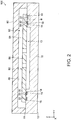
- Fig. 2 is a cross-sectional view schematically showing a cross section taken along the line A-A in Fig. 1 .
- Fig. 3 is an enlarged cross-sectional view of a portion B in Fig. 2 .
- Fig. 4 is a cross-sectional view schematically showing a cross section taken along the line C-C in Fig. 1 .
- Fig. 1 shows a lid body 60 in perspective.
- Fig. 1 shows a lid body 60 in perspective.
- a metal layer 32 a noble metal layer 34 , an adhesion layer 36, and an insulating layer 38 are omitted.
- an X axis, a Y axis, and a Z axis are shown as three axes orthogonal to each other.
- the physical quantity sensor 100 is an acceleration sensor that measures acceleration in the horizontal direction (X-axis direction) will be described.
- the physical quantity sensor 100 includes a base substrate 10, a sensor substrate 80, and the lid body 60.
- the base substrate 10 includes multilayered film wirings 20, 22, and 24 made of the metal layer 32 and the noble metal layer 34, the adhesion layer 36, the insulating layer 38, and connection terminals 50, 52, and 54.
- the sensor substrate 80 includes a bonding portion 30, a silicide layer 31, fixed portions 81 and 82, connecting portions 84 and 85, a movable portion 86, a movable electrode portion 87 as a movable electrode, a first fixed electrode portion 88 and a second fixed electrode portion 89 as fixed electrodes.
- the material of the base substrate 10 is, for example, an insulating material, specifically, glass or the like.
- the base substrate 10 has a first surface (specifically, an upper surface) 11 and a second surface (specifically, a lower surface) 12 opposite to the first surface 11.
- the first surface 11 faces a +Z-axis direction
- the second surface 12 faces a -Z-axis direction.
- a recess portion 13 is provided on the first surface 11.
- Groove portions 14, 15, and 16 are further provided on the first surface 11.
- the movable portion 86 and the movable electrode portion 87 of the sensor substrate 80 are disposed above the recess portion 13 (on the +Z-axis direction side).
- the recess portion 13 allows the movable portion 86 and the movable electrode portion 87 to move in a desired direction without being obstructed by the base substrate 10.
- the planar shape (shape when viewed from the Z-axis direction) of the recess portion 13 is not particularly limited, but in the example shown in Fig. 1 , the shape is rectangular.
- the groove portion 14 is provided so as to extend along the outer periphery of the recess portion 13 in a plan view (viewed from the Z-axis direction).
- the groove portion 14 extends from the inside to the outside of a cavity 62 surrounded by the base substrate 10 and the lid body 60 .
- the groove portion 14 has, for example, a planar shape corresponding to the planar shape of the wiring 20 and the connection terminal 50.
- the groove portion 15 is provided so as to extend along the outer periphery of the recess portion 13 in a plan view. In the example shown in Fig. 1 , the groove portion 15 is provided outside the groove portion 14 so as to surround the groove portion 14. The groove portion 15 extends from the inside to the outside of the cavity 62.
- the groove portion 15 has, for example, a planar shape corresponding to the planar shape of the wiring 22 and the connection terminal 52.
- the groove portion 16 extends from the inside to the outside of the cavity 62.
- the groove portion 16 has, for example, a planar shape corresponding to the planar shape of the wiring 24 and the connection terminal 54.
- a plurality of projection portions 18 are provided in the groove portions 14, 15, and 16, and the wirings 20, 22, and 24 provided on the projection portion 18 and the sensor substrate 80 are electrically connected via the silicide layer 31.
- the wirings 20, 22, and 24 are provided in the groove portions 14, 15, and 16 and on the projection portion 18 provided in the groove portions 14, 15, and 16.
- the wiring 20 is provided in the groove portion 14. More specifically, the wiring 20 is made of the metal layer 32 and the noble metal layer 34 and is provided on a bottom surface (the surface of the base substrate 10 defining the groove portion 14) 14a of the groove portion 14. As shown in Fig. 3 , the wiring 20 is electrically connected to the first fixed electrode portion 88 of the sensor substrate 80 via the silicide layer 31 of the bonding portion 30 in the projection portion 18 provided in the groove portion 14.
- the wiring 22 is provided in the groove portion 15. More specifically, the wiring 22 is made of the metal layer 32 and the noble metal layer 34 and is provided on a bottom surface 15a of the groove portion 15. The wiring 22 is electrically connected to the second fixed electrode portion 89 of the sensor substrate 80 via the silicide layer 31 of the bonding portion 30 in the projection portion 18 provided in the groove portion 15.
- the wiring 24 is provided in the groove portion 16. More specifically, the wiring 24 is made of the metal layer 32 and the noble metal layer 34 and is provided on a bottom surface 16a of the groove portion 16. As shown in Fig. 4 , the wiring 24 is electrically connected to the first fixed portion 81 of the sensor substrate 80 via the silicide layer 31 of the bonding portion 30 in the projection portion 18 provided in the groove portion 16.
- the thickness (size in the Z-axis direction) of the wirings 20, 22, and 24 is, for example, 20 nm or more and 1 ⁇ m or less
- the thickness of the metal layer 32 is, for example, 10 nm or more and 800 nm or less
- the thickness of the noble metal layer 34 is, for example, 10 nm or more and 200 nm or less.
- the thickness of the noble metal layer 34 is set to 200 nm or less, voids due to excessive silylation are hardly generated, and disconnection at the corners of the projection portion 18 is hardly caused, and therefore, it is possible to sufficiently secure electrical connection between the sensor substrate 80 and the wirings 20, 22, and 24.
- the material of the noble metal layer 34 is, for example, one of Ru, Pt, Pd, Ir, Rh, and Os, or a plurality of materials. Therefore, the sensor substrate 80 and the silicide layer 31 may be formed, and the bonding portion 30 of the sensor substrate 80 and the noble metal layer 34 of the wirings 20, 22, and 24 may be electrically connected.
- the silicide layer 31 is provided between the bonding portion 30 of the sensor substrate 80 and the wirings 20, 22, and 24 and connects the bonding portion 30 of the sensor substrate 80 and the wirings 20, 22, and 24. More specifically, the silicide layer 31 is formed between the bonding portion 30 of the first fixed electrode portion 88 and the wiring 20, between the bonding portion 30 of the second fixed electrode portion 89 and the wiring 22, and between the bonding portion 30 of the first fixed portion 81 and the wiring 24.
- the silicide layer 31 is formed by silicon (silicon of a silicon substrate 80a to be the sensor substrate 80) at the bonding portion 30 of the sensor substrate 80 reacting with the noble metal layer 34 of the wirings 20, 22, and 24. More specifically, at the time of anodically bonding the silicon substrate 80a (see Fig. 8 ) to be the sensor substrate 80 and the base substrate 10, silicon at the bonding portion 30 of the silicon substrate 80a reacts with the noble metal layer 34, thereby forming the silicide layer 31.
- the thickness of the silicide layer 31 is not particularly limited, is appropriately determined depending on the thickness of the noble metal layer 34, anodic bonding conditions (temperature and time), and the like, and is, for example, 10 nm or more and 200 nm or less.
- the adhesion layer 36 is provided so as to cover a part of the wirings 20, 22, and 24. More specifically, the adhesion layer 36 is provided so as to cover an area covering the projection portion 18 as shown in Fig. 3 , or cover the wirings 20, 22, and 24 as shown in Fig. 4 .
- the material of the adhesion layer 36 is, for example, one of Ti, TiW, W, TiN, Ta, TaW, TaN, Ni, and Co, or a plurality of materials.
- the adhesion layer 36 may enhance the adhesion between the noble metal layer 34 and the insulating layer 38 in the wirings 20, 22, and 24, and peeling of the insulating layer 38 due to heat generated at the time of bonding the substrates to each other or mounting on the external substrate may be reduced.
- the thickness of the adhesion layer 36 is, for example, 10 nm or more and 200 nm or less.
- the insulating layer 38 is provided so as to cover the adhesion layer 36. More specifically, the insulating layer 38 is stacked on the adhesion layer 36 so as to avoid an area covering the projection portion 18 and an area where the connection terminals 50, 52, and 54 are disposed.
- the material of the insulating layer 38 is one of SiO 2 , SiOF, SiOC, SiON, SiH, HfO 2 , Al 2 O 3 , La 2 O 3 , TiO 2 , Ta 2 O 5 , and DLC (Diamond ⁇ Like ⁇ Carbon), or a plurality of materials.
- the insulating layer 38 may prevent a foreign matter from adhering to the wirings 20 and 22 and short-circuiting between the wirings 20 and 22 and the fixed electrode.
- the thickness of the insulating layer 38 is, for example, 10 nm or more and 300 nm or less.
- the area covering the projection portion 18 is the noble metal layer 34 in which the layer in contact with the bonding portion 30 forms the silicide layer 31, and the portion between the noble metal layer 34 and the base substrate 10 is the metal layer 32.
- the metal layer 32, the noble metal layer 34, the adhesion layer 36, and the insulating layer 38 are stacked in this order from the base substrate 10 side in the area excluding the projection portion 18.
- connection terminals 50, 52, and 54 are provided in the groove portions 14, 15, and 16, respectively.
- the connection terminals 50, 52, and 54 are connected to the wirings 20, 22, and 24, respectively. Therefore, the connection terminal 50 is electrically connected to the first fixed electrode portion 88.
- the connection terminal 52 is electrically connected to the second fixed electrode portion 89.
- the connection terminal 54 is electrically connected to the first fixed portion 81.
- connection terminals 50, 52, and 54 are provided (on the outside of the cavity 62) at a position not overlapping with the lid body 60 in a plan view.
- Materials of the connection terminals 50, 52, and 54 are, for example, the same as the wirings 20, 22, 24.
- the lid body 60 is mounted (bonded) on the base substrate 10 (on the first surface 11).
- the lid body 60 has a container-like shape, and the cavity 62 may be formed by being bonded to the base substrate 10.
- a gap 2 gap in the groove portion 16 between the insulating layer 38 and the lid body 60 shown in Fig. 4 may be filled with an adhesive member (not shown) or the like, and in this case, the cavity 62 may be hermetically sealed in an inert gas (for example, nitrogen gas) atmosphere.
- an inert gas for example, nitrogen gas
- the material of the lid body 60 is, for example, silicon, glass, or the like.
- the method of bonding the lid body 60 and the base substrate 10 is not particularly limited.
- the base substrate 10 and the lid body 60 may be anodically bonded.
- the sensor substrate 80 is supported (on the first surface 11) on the base substrate 10.
- the sensor substrate 80 is housed in the cavity 62.
- the material of the sensor substrate 80 is silicon to which conductivity is imparted by doping impurities such as phosphorus and boron.
- the movable portion 86 of the sensor substrate 80 is displaced in the X-axis direction (+X-axis direction or -X-axis direction) while elastically deforming the connecting portions 84 and 85 according to the change in the acceleration in the X-axis direction.
- the sizes of the gap between the movable electrode portion 87 and the first fixed electrode portion 88 and the gap between the movable electrode portion 87 and the second fixed electrode portion 89 change. That is, with such displacement, the magnitudes of the electrostatic capacitance between the movable electrode portion 87 and the first fixed electrode portion 88 and the electrostatic capacitance between the movable electrode portion 87 and the second fixed electrode portion 89 change.
- the physical quantity sensor 100 may measure the acceleration in the X-axis direction based on the change in the electrostatic capacitance.
- the first fixed portion 81 and the second fixed portion 82 are bonded to the first surface 11 of the base substrate 10.
- the fixed portions 81 and 82 are provided so as to straddle the outer peripheral edge of the recess portion 13 in a plan view.
- the planar shape of the fixed portions 81 and 82 is, for example, rectangular.
- the first fixed portion 81 is provided so as to straddle the groove portion 16. In the example shown in Fig. 1 , a part of the first fixed portion 81 overlaps with the groove portion 16. As shown in Fig. 4 , the first fixed portion 81 is electrically connected to the connection terminal 54 via the silicide layer 31 and the wiring 24.
- the movable portion 86 is provided between the first fixed portion 81 and the second fixed portion 82.
- the planar shape of the movable portion 86 is a rectangle having a long side along the X axis.
- the connecting portions 84 and 85 connect the movable portion 86 and the fixed portions 81 and 82. More specifically, the first connecting portion 84 connects the movable portion 86 and the first fixed portion 81, and the second connecting portion 85 connects the movable portion 86 and the second fixed portion 82.
- the connecting portions 84 and 85 have a desired spring constant and are configured to displace the movable portion 86 in the X-axis direction.
- the first connecting portion 84 is constituted by two beams 84a and 84b having a shape extending in the X-axis direction while reciprocating in the Y-axis direction.
- the second connecting portion 85 is constituted by two beams 85a and 85b having a shape extending in the X-axis direction while reciprocating in the Y-axis direction.
- the movable electrode portion 87 as a movable electrode is connected to the movable portion 86.
- the movable electrode portion 87 is provided in the movable portion 86.
- a plurality of movable electrode portions 87 are provided.
- the movable electrode portion 87 protrudes in the +Y-axis direction and the -Y-axis direction from the movable portion 86 and is arranged in the X-axis direction so as to form a comb teeth shape.
- the fixed electrode portions 88 and 89 as fixed electrodes are provided on the base substrate 10 and are arranged to face the movable electrode portion 87.
- One end of each of the fixed electrode portions 88 and 89 is bonded to the first surface 11 of the base substrate 10 as a fixed end and the other end thereof extends to the movable portion 86 side as a free end.
- a plurality of fixed electrode portions 88 and 89 are provided.
- the fixed electrode portions 88 and 89 are alternately arranged in the X-axis direction so as to form a comb teeth shape.
- the fixed electrode portions 88 and 89 are provided to be opposed to the movable electrode portion 87 with a space therebetween. In the example shown in Fig.
- the first fixed electrode portion 88 is disposed on one side (the -X-axis direction side) of the movable electrode portion 87, and the second fixed electrode portion 89 is disposed on the other side (the +X-axis direction side).
- the area of the first fixed electrode portion 88 that faces the movable electrode portion 87 is the same as the area that faces the movable electrode portion 87 of the second fixed electrode portion 89.
- the first fixed electrode portion 88 is provided so as to straddle the groove portions 14 and 15. In the example shown in Fig. 1 , the first fixed electrode portion 88 intersects the groove portions 14 and 15. The first fixed electrode portion 88 is electrically connected to the connection terminal 50 via the silicide layer 31 and the wiring 20.
- the second fixed electrode portion 89 is provided so as to straddle the groove portions 14 and 15. In the example shown in Fig. 1 , the second fixed electrode portion 89 intersects the groove portions 14 and 15. The second fixed electrode portion 89 is electrically connected to the connection terminal 52 via the silicide layer 31 and the wiring 22. The second fixed electrode portion 89 is electrically separated from the first fixed electrode portion 88.
- the fixed portions 81 and 82, the connecting portions 84 and 85, the movable portion 86, and the movable electrode portion 87 are integrally provided.
- the method for bonding the fixed portions 81 and 82, the fixed electrode portions 88 and 89, and the base substrate 10 is not particularly limited.
- the fixed portions 81 and 82, the fixed electrode portions 88 and 89, and the base substrate 10 are anodically bonded.
- the electrostatic capacitance between the movable electrode portion 87 and the first fixed electrode portion 88 may be measured by using the connection terminals 50 and 54. Furthermore, in the physical quantity sensor 100, the electrostatic capacitance between the movable electrode portion 87 and the second fixed electrode portion 89 may be measured by using the connection terminals 52 and 54. As described above, in the physical quantity sensor 100, the electrostatic capacitance between the movable electrode portion 87 and the first fixed electrode portion 88 and the electrostatic capacitance between the movable electrode portion 87 and the second fixed electrode portion 89 are separately measured, and it is possible to measure the physical quantity (acceleration) with high accuracy based on the measurement results.
- the electrostatic capacitance between the movable electrode portion 87 and the first fixed electrode portion 88 and the electrostatic capacitance between the movable electrode portion 87 and the second fixed electrode portion 89 are monitored and differential measurement is performed, and therefore, it is possible to measure acceleration with high accuracy.
- the physical quantity sensor 100 is described as an acceleration sensor that measures the acceleration in the X-axis direction, but the physical quantity sensor 100 according to the invention may be an acceleration sensor that measures acceleration in the Y-axis direction or an acceleration sensor that measures acceleration in the vertical direction (Z-axis direction).
- the physical quantity sensor 100 according to the invention is not limited to an acceleration sensor and may be a gyro sensor that measures angular velocity, for example.
- the physical quantity sensor 100 has the following features, for example.
- the wirings 20, 22, and 24 provided in the projection portion 18 are multilayered films of the noble metal layer 34 and the metal layer 32 forming the silicide layer 31, it is possible to adjust the thickness of the noble metal layer 34 and the metal layer 32. Therefore, by thickening the metal layer 32, the noble metal layer 34 may be thinned, and therefore, excessive silylation does not occur and there are fewer moving atoms. Therefore, since no void is generated in the silicide layer 31, cracking hardly occurs, and the reliability of the electrical connection between the sensor substrate 80 and the wirings 20, 22, and 24 may be improved.
- the insulating layer 38 is formed on the noble metal layer 34 via the adhesion layer 36, it is possible to improve the adhesion between the insulating layer 38 and the noble metal layer 34 and reduce the peeling of the insulating layer 38 due to heat generated at the time of bonding the substrates to each other or at the time of mounting on the external substrate. Therefore, it is possible to obtain the physical quantity sensor 100 having high reliability.
- the thickness of the noble metal layer 34 is, for example, 10 nm or more and 200 nm or less and the thickness of the noble metal layer 34 is 10 nm or more, it is possible to form a sufficient continuous film and secure the electrical connection between the sensor substrate 80 and the wirings 20, 22, and 24.
- the thickness of the noble metal layer 34 is 200 nm or less, voids due to excessive silylation are hardly generated, and disconnection at the corner portions of the projection portion 18 is hardly caused, and therefore, it is possible to secure the electrical connection between the sensor substrate 80 and the wirings 20, 22, and 24 via the silicide layer 31.
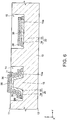
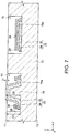
- Figs. 5 to 8 are cross-sectional views schematically showing a manufacturing process of the physical quantity sensor 100 according to the first embodiment and correspond to Fig. 3 .
- the base substrate 10 provided with the recess portion 13, the groove portions 14, 15, and 16, and the projection portion 18 (see Figs. 2 and 4 ) is prepared.
- the recess portion 13, the groove portions 14, 15, and 16, and the projection portion 18 are formed by, for example, a photolithography technique and an etching technique.
- the wirings 20, 22, and 24 are formed in the groove portions 14, 15, and 16, respectively, by depositing the metal layer 32 and the noble metal layer 34 in this order.
- the metal layer 32 and the noble metal layer 34 are formed by, for example, a film deposition by a sputtering method or a chemical vapor deposition (CVD) method, a patterning by a photolithography technique and an etching technique, and a forming method by a lift-off method or the like.
- the thickness of the metal layer 32 is, for example, 10 nm or more and 800 nm or less
- a thickness T of the noble metal layer 34 is, for example, 10 nm or more and 200 nm or less.
- the adhesion layer 36 and the insulating layer 38 are formed in this order on the wirings 20, 22, and 24 by deposition.
- the adhesion layer 36 and the insulating layer 38 are formed by, for example, a film deposition by a sputtering method or a CVD method and a patterning by a photolithography technique and an etching technique.
- the thickness of the adhesion layer 36 is, for example, 10 nm or more and 200 nm or less
- the thickness of the insulating layer 38 is, for example, 10 nm or more and 300 nm or less.
- the insulating layer 38 in an area covering the projection portion 18 and an area where the connection terminals 50, 52, and 54 (see Fig. 1 ) are formed is removed. Removal of the insulating layer 38 is performed by a photolithography technique and an etching technique.
- the noble metal layer 34 at a position facing the bonding portion 30 of the sensor substrate 80 is formed so as to protrude upward (+Z-axis direction side) from the first surface 11 of the base substrate 10. That is, the metal layer 32 and the noble metal layer 34 are formed so that a total thickness (height) D2 of the thickness (height) of the projection portion 18, the thickness of the metal layer 32, and the thickness of the noble metal layer 34 is set larger than a depth D1 of the groove portion 14.
- the projection portion 18 of the groove portion 15 and the projection portion 18 of the groove portion 16 have the same configuration.
- the noble metal layer 34 on the projection portion 18 and the silicon at the bonding portion 30 of the sensor substrate 80 may be reliably brought into contact, and the silicide layer 31 may be formed on the bonding portion 30 of the sensor substrate 80.
- connection terminals 50, 52, and 54 are formed on the wirings 20, 22, and 24, respectively.
- the connection terminals 50, 52, and 54 are formed in the same manner as the wirings 20, 22, and 24, for example.
- the silicon substrate 80a is prepared, and the silicon substrate 80a is mounted on the base substrate 10 so that the noble metal layer 34 and the bonding portion 30 of the silicon substrate 80a come into contact with each other.
- the base substrate 10 and the silicon substrate 80a are bonded. More specifically, the first surface 11 of the base substrate 10 and a third surface (the surface facing in the -Z-axis direction in the illustrated example) 80b of the silicon substrate 80a are anodically bonded.
- silicon at the bonding portion 30 of the silicon substrate 80a diffuses into the noble metal layer 34, and the noble metal layer 34 diffuses to the bonding portion 30 of the silicon substrate 80a.
- silicon at the bonding portion 30 of the silicon substrate 80a may react with, for example, Pt (platinum) of the noble metal layer 34 to form the silicide layer (platinum silicide layer) 31.
- the silicon substrate 80a is ground by, for example, a grinding machine to form a thin film, and then patterned into a desired shape to form a sensor substrate 80.
- Patterning is performed by a photolithography technique and an etching technique (dry etching), and the Bosch method may be used as a more specific etching technique.
- the fixed portions 81 and 82, the connecting portions 84 and 85, the movable portion 86, and the movable electrode portion 87 may be integrally formed by patterning (etching) the silicon substrate 80a.
- the lid body 60 is bonded to the base substrate 10, and the sensor substrate 80 is housed in the cavity 62 formed by the base substrate 10 and the lid body 60.
- Bonding between the base substrate 10 and the lid body 60 is performed by using, for example, anodic bonding, an adhesive, or the like. By performing this process in an inert gas atmosphere, it is possible to fill the cavity 62 with inert gas.
- the physical quantity sensor 100 according to the first embodiment may be manufactured.
- Fig. 9 is a cross-sectional view schematically showing a schematic structure of the physical quantity sensor 100a according to the second embodiment and corresponds to Fig. 3 .
- points different from the example of the physical quantity sensor 100 according to the first embodiment will be described, and description of similar points will be omitted.
- the insulating layer 38 is constituted by one layer.
- the insulating layer 39 is constituted by two layers.
- the insulating layer 39 is provided by stacking a first insulating layer 38a and a second insulating layer 38b on the adhesion layer 36.
- the sensor substrate 80 is formed by etching, it is possible to improve etching resistance by forming the insulating layer 39 in a two-layer structure.
- the insulating layer 39 is constituted by two layers of the first insulating layer 38a and the second insulating layer 38b, in a case where the sensor substrate 80 is formed by etching, it is possible to improve etching resistance. In addition, it is possible to relieve the residual stress of the insulating layer 39 and reduce the warping of the base substrate 10 by forming the insulating layer 39 with two layers using the first insulating layer 38a and the second insulating layer 38b having different materials.
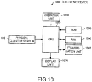
- Fig. 10 is a functional block diagram of the electronic device 1000 according to the embodiment.
- the electronic device 1000 includes the physical quantity sensors 100 and 100a according to the invention.
- the physical quantity sensor 100 according to the invention is included will be described.
- the electronic device 1000 further includes an arithmetic processing unit (CPU) 1020, an operation unit 1030, a read-only memory (ROM) 1040, a random-access memory (RAM) 1050, a communication unit 1060, and a display unit 1070.
- the electronic device 1000 of the embodiment may be configured such that part of the components (each unit) in Fig. 10 is omitted or changed, or other components are added.
- the arithmetic processing unit 1020 performs various calculation processing and control processing according to a program stored in the ROM 1040 or the like. More specifically, the arithmetic processing unit 1020 performs various processing according to the output signal of the physical quantity sensor 100, the operation signal from the operation unit 1030, processing of controlling the communication unit 1060 to perform data communication with an external device, and processing of transmitting a display signal for displaying various kinds of information on the display unit 1070.
- the operation unit 1030 is an input device constituted by operation keys, button switches, and the like and outputs an operation signal corresponding to an operation by a user to the arithmetic processing unit 1020.
- the ROM 1040 stores programs, data, and the like for the arithmetic processing unit 1020 to perform various calculation processing and control processing.
- the RAM 1050 is used as a work area of the arithmetic processing unit 1020 and temporarily stores programs and data read from the ROM 1040, data input from the physical quantity sensor 100, data input from the operation unit 1030, calculation results executed by the arithmetic processing unit 1020 according to various programs, and the like.
- the communication unit 1060 performs various controls for establishing data communication between the arithmetic processing unit 1020 and the external device.
- the display unit 1070 is a display device constituted by a liquid crystal display (LCD) and the like and displays various kinds of information based on a display signal input from the arithmetic processing unit 1020.
- a touch panel functioning as the operation unit 1030 may be provided on the display unit 1070.
- the electronic device 1000 various kinds of electronic devices are conceivable, such as personal computers (for example, a mobile type personal computer, a laptop type personal computer, and a tablet type personal computer), mobile terminals such as smart phones and mobile phones, digital still cameras, ink jet type ejecting apparatuses (for example, an ink jet printer), storage area network devices such as routers and switches, local area network devices, devices for mobile terminal base stations, televisions, video cameras, video recorders, car navigation devices, real time clock device, pager, electronic notebooks (communication function included), electronic dictionaries, calculators, electronic game devices, game controllers, word processors, workstations, video phones, TV monitors for crime prevention, electronic binoculars, POS terminals, medical devices (for example, an electronic clinical thermometer, a blood pressure monitor, a blood glucose meter, an electrocardiogram measuring device, a ultrasonic diagnostic device, and an electronic endoscope), fish finders, various measuring instruments, instruments (for example, instruments of a vehicle, an aircraft, a ship), flight
- Fig. 11 is a diagram showing an example of an appearance of a smartphone which is an example of the electronic device 1000.
- a smartphone as the electronic device 1000 includes buttons as the operation unit 1030 and an LCD as the display unit 1070.
- Fig. 12 is a diagram showing an example of an appearance of a wrist-worn portable device (wearable device) which is an example of the electronic device 1000.
- the wearable device which is the electronic device 1000 includes an LCD as the display unit 1070.
- a touch panel functioning as the operation unit 1030 may be provided on the display unit 1070.
- a mobile device which is the electronic device 1000, has a position sensor such as a GPS receiver (GPS: Global Positioning System), for example, and may measure a moving distance and a movement trajectory of the user.
- GPS Global Positioning System
- Fig. 13 is a plan view schematically showing an automobile as the vehicle 1100 according to the embodiment.
- the vehicle 1100 according to the embodiment includes the physical quantity sensors 100 and 100a according to the invention.
- the vehicle 1100 including the physical quantity sensor 100 according to the invention will be described.
- the vehicle 1100 according to the embodiment is configured to further include a controller 1120 that performs various controls such as an engine system, a brake system, a keyless entry system, and the like, a controller 1130, a controller 1140, a battery 1150, and a backup battery 1160.
- the vehicle 1100 according to the embodiment may be configured such that a part of the constituent elements (each unit) shown in Fig. 13 is omitted or changed, or other constituent elements are added.
- vehicle 1100 various vehicles are conceivable, and examples thereof include an automobile (including an electric car), an aircraft such as a jet machine and a helicopter, a ship, a rocket, an artificial satellite, and the like.
- the invention includes substantially the same configuration as the configuration described in the embodiments (for example, a configuration having the same function, method, and result, or a configuration having the same object and effect).
- the invention includes a configuration in which non-essential parts of the configuration described in the embodiments are replaced.
- the invention includes a configuration that achieves the same effects as the configurations described in the embodiments or a configuration that may achieve the same object.
- the invention includes a configuration in which well-known techniques are added to the configurations described in the embodiments.
Landscapes
- Physics & Mathematics (AREA)
- General Physics & Mathematics (AREA)
- Engineering & Computer Science (AREA)
- Radar, Positioning & Navigation (AREA)
- Remote Sensing (AREA)
- Pressure Sensors (AREA)
Abstract
In a physical quantity sensor, wirings provided in a projection portion and a bonding portion form a silicide layer and are electrically connected, the wirings are multilayered films, the area covering the projection portion is a noble metal layer in which the layer in contact with the bonding portion forms a silicide layer, a portion between the noble metal layer and a base substrate is a metal layer, and the metal layer, the noble metal layer, an adhesion layer, and an insulating layer are stacked in this order from the base substrate side in the area excluding the projection portion.
Description
- The present invention relates to a physical quantity sensor, an electronic device, and a vehicle.
- In the related art, as a physical quantity sensor that measures physical quantities such as acceleration and angular velocity, there is known a structure having a fixed electrode and a movable electrode arranged side by side with a gap with respect to the fixed electrode and displaceable in a fixed direction. With such a physical quantity sensor, the gap between the fixed electrode and the movable electrode changes in accordance with the displacement of the movable electrode and a change in electrostatic capacitance occurring between the fixed electrode and the movable electrode is measured by the change in the gap so that the changes in physical quantities such as acceleration and angular velocity are measured.
- In
JP-A-2014-16165 - However, in the physical quantity sensor described in
JP-A-2014-16165 - An advantage of some aspects of the invention is to solve at least a part of the problems described above, and the invention can be implemented as the following embodiments or application examples.
- Aa physical quantity sensor according to this application example includes a base substrate that includes a groove portion for forming a wiring and a projection portion in the groove portion, and a sensor substrate that includes a bonding portion connected to the wiring provided on the projection portion and a fixed electrode and a movable electrode for measuring a physical quantity, in which the base substrate is an insulating material, the sensor substrate is silicon, the wiring provided on the projection portion and the bonding portion are electrically connected by forming a silicide layer, the wirings are multilayered films, the area covering the projection portion is a noble metal layer in which the layer in contact with the bonding portion forms a silicide layer, a portion between the noble metal layer and the base substrate is a metal layer, and the metal layer, the noble metal layer, an adhesion layer, and an insulating layer are stacked in this order from the base substrate side in the area excluding the projection portion.
- According to this application example, since the wirings provided in the projection portion are multilayered films of the noble metal layer and the metal layer forming the silicide layer, it is possible to adjust the thickness of the noble metal layer and the metal layer. Therefore, by thickening the metal layer, the noble metal layer may be thinned, and therefore, excessive silylation does not occur and there are fewer moving atoms. Therefore, since no void is generated in the silicide layer, cracking hardly occurs, and the reliability of the electrical connection between the sensor substrate and the wirings may be improved. Therefore, it is possible to obtain the physical quantity sensor having high reliability.
- In the physical quantity sensor described in the application example, it is preferable that the thickness of the noble metal layer is 10 nm or more and 200 nm or less.
- According to this application example, since the thickness of the noble metal layer is 10 nm or more, a sufficient continuous film may be formed, and electrical connection between the sensor substrate and the wirings may be secured. In addition, the thickness of the noble metal layer is 200 nm or less, voids due to excessive silylation are hardly generated, and disconnection at the corner portions of the projection portion is hardly caused, and therefore, it is possible to secure the electrical connection between the sensor substrate and the wirings via the silicide layer.
- In the physical quantity sensor described in the application example, it is preferable that the noble metal layer is made of one of Ru, Pt, Pd, Ir, Rh, and Os, or a plurality of materials.
- According to this application example, since the noble metal layer is made of one of Ru, Pt, Pd, Ir, Rh, and Os or a plurality of materials, the sensor substrate and the silicide layer may be formed, and the wirings may be electrically connected with the sensor substrate.
- In the physical quantity sensor according to the application example, it is preferable that the insulating layer is made of one of SiO2, SiOF, SiOC, SiON, SiH, HfO2, Al2O3, La2O3, TiO2, Ta2O5, and DLC (Diamond·Like·Carbon), or a plurality of materials.
- According to this application example, since the insulating layer is made of one of SiO2, SiOF, SiOC, SiON, SiH, HfO2, Al2O3, La2O3, TiO2, Ta2O5, and DLC (Diamond·Like·Carbon), or a plurality of materials, it is possible to prevent foreign matter from adhering to the wirings and short-circuiting between the wirings and the fixed electrode.
- In the physical quantity sensor described in the application example, it is preferable that the adhesion layer is made of one of Ti, TiW, W, TiN, Ta, TaW, TaN, Ni, and Co, or a plurality of materials.
- According to this application example, since the adhesion layer is made of one or more materials such as Ti, TiW, W, TiN, Ta, TaW, TaN, Ni, and Co, it is possible to improve the adhesion between the insulating layer and the noble metal layer and reduce the peeling of the insulating layer due to heat generated at the time of bonding the substrates to each other or at the time of mounting on an external substrate.
- In the physical quantity sensor described in the application example, it is preferable that the insulating layer is in two layers.
- According to this application example, since the insulating layer in two layers, it is possible to improve etching resistance in a case where the sensor substrate is formed by etching. In addition, it is possible to relieve the residual stress of the insulating layer and to reduce warping of the substrate by using two insulating layers having different materials.
- An electronic device according to this application example includes the physical quantity sensor described in the application example.
- According to this application example, it is possible to provide an electronic device with higher performance by using a physical quantity sensor having high measurement sensitivity for the electronic device.
- A vehicle according to this application example includes the physical quantity sensor described in the application example.
- According to this application example, it is possible to provide a vehicle with higher performance by using a physical quantity sensor having high measurement sensitivity for the vehicle.
- The invention will be described with reference to the accompanying drawings, wherein like numbers reference like elements.
-
Fig. 1 is a plan view schematically showing a schematic structure of a physical quantity sensor according to a first embodiment. -
Fig. 2 is a cross-sectional view schematically showing a cross section taken along the line A-A inFig. 1 . -
Fig. 3 is an enlarged cross-sectional view of a portion B inFig. 2 . -
Fig. 4 is a cross-sectional view schematically showing a cross section taken along the line C-C inFig. 1 . -
Fig. 5 is a cross-sectional view schematically showing a manufacturing process of the physical quantity sensor according to a first embodiment. -
Fig. 6 is a cross-sectional view schematically showing a manufacturing process of the physical quantity sensor according to a first embodiment. -
Fig. 7 is a cross-sectional view schematically showing a manufacturing process of the physical quantity sensor according to a first embodiment. -
Fig. 8 is a cross-sectional view schematically showing a manufacturing process of the physical quantity sensor according to a first embodiment. -
Fig. 9 is a cross-sectional view schematically showing a physical quantity sensor according to a second embodiment. -
Fig. 10 is a functional block diagram of an electronic device according to an embodiment of the invention. -
Fig. 11 is a plan view schematically showing an appearance of a smartphone which is an example of an electronic device according to an embodiment of the invention. -
Fig. 12 is a perspective view schematically showing an appearance of a wearable device which is an example of an electronic device according to an embodiment of the invention. -
Fig. 13 is a plan view schematically showing a vehicle according to an embodiment of the invention. - Hereinafter, embodiments of the invention will be described in detail with reference to drawings. In each diagram shown below, in order to make the constituent elements large enough to be recognized on the drawing, sometimes the dimension and ratio of each constituent element are described as being different from the actual constituent elements as appropriate.
- First, a
physical quantity sensor 100 according to a first embodiment will be described with reference toFigs. 1 to 4 .Fig. 1 is a plan view schematically showing a schematic structure of a physical quantity sensor according to a first embodiment.Fig. 2 is a cross-sectional view schematically showing a cross section taken along the line A-A inFig. 1 .Fig. 3 is an enlarged cross-sectional view of a portion B inFig. 2 .Fig. 4 is a cross-sectional view schematically showing a cross section taken along the line C-C inFig. 1 . For the sake of convenience,Fig. 1 shows alid body 60 in perspective. In addition, inFig. 2 , ametal layer 32, anoble metal layer 34, anadhesion layer 36, and an insulatinglayer 38 are omitted. Furthermore, inFigs. 1 to 4 andFigs. 5 to 9 shown below, an X axis, a Y axis, and a Z axis are shown as three axes orthogonal to each other. - Hereinafter, a case where the
physical quantity sensor 100 is an acceleration sensor that measures acceleration in the horizontal direction (X-axis direction) will be described. - As shown in
Figs. 1 to 4 , thephysical quantity sensor 100 includes abase substrate 10, asensor substrate 80, and thelid body 60. Thebase substrate 10 includesmultilayered film wirings metal layer 32 and thenoble metal layer 34, theadhesion layer 36, the insulatinglayer 38, andconnection terminals sensor substrate 80 includes abonding portion 30, asilicide layer 31, fixedportions portions movable portion 86, amovable electrode portion 87 as a movable electrode, a firstfixed electrode portion 88 and a secondfixed electrode portion 89 as fixed electrodes. - The material of the
base substrate 10 is, for example, an insulating material, specifically, glass or the like. As shown inFig. 2 , thebase substrate 10 has a first surface (specifically, an upper surface) 11 and a second surface (specifically, a lower surface) 12 opposite to thefirst surface 11. In the illustrated example, thefirst surface 11 faces a +Z-axis direction, and thesecond surface 12 faces a -Z-axis direction. On thefirst surface 11, arecess portion 13 is provided.Groove portions first surface 11. - The
movable portion 86 and themovable electrode portion 87 of thesensor substrate 80 are disposed above the recess portion 13 (on the +Z-axis direction side). Therecess portion 13 allows themovable portion 86 and themovable electrode portion 87 to move in a desired direction without being obstructed by thebase substrate 10. The planar shape (shape when viewed from the Z-axis direction) of therecess portion 13 is not particularly limited, but in the example shown inFig. 1 , the shape is rectangular. - As shown in
Fig. 1 , thegroove portion 14 is provided so as to extend along the outer periphery of therecess portion 13 in a plan view (viewed from the Z-axis direction). Thegroove portion 14 extends from the inside to the outside of acavity 62 surrounded by thebase substrate 10 and thelid body 60 . Thegroove portion 14 has, for example, a planar shape corresponding to the planar shape of thewiring 20 and theconnection terminal 50. - The
groove portion 15 is provided so as to extend along the outer periphery of therecess portion 13 in a plan view. In the example shown inFig. 1 , thegroove portion 15 is provided outside thegroove portion 14 so as to surround thegroove portion 14. Thegroove portion 15 extends from the inside to the outside of thecavity 62. Thegroove portion 15 has, for example, a planar shape corresponding to the planar shape of thewiring 22 and theconnection terminal 52. - The
groove portion 16 extends from the inside to the outside of thecavity 62. Thegroove portion 16 has, for example, a planar shape corresponding to the planar shape of thewiring 24 and theconnection terminal 54. - A plurality of
projection portions 18 are provided in thegroove portions wirings projection portion 18 and thesensor substrate 80 are electrically connected via thesilicide layer 31. - The
wirings groove portions projection portion 18 provided in thegroove portions - The
wiring 20 is provided in thegroove portion 14. More specifically, thewiring 20 is made of themetal layer 32 and thenoble metal layer 34 and is provided on a bottom surface (the surface of thebase substrate 10 defining the groove portion 14) 14a of thegroove portion 14. As shown inFig. 3 , thewiring 20 is electrically connected to the firstfixed electrode portion 88 of thesensor substrate 80 via thesilicide layer 31 of thebonding portion 30 in theprojection portion 18 provided in thegroove portion 14. - The
wiring 22 is provided in thegroove portion 15. More specifically, thewiring 22 is made of themetal layer 32 and thenoble metal layer 34 and is provided on abottom surface 15a of thegroove portion 15. Thewiring 22 is electrically connected to the secondfixed electrode portion 89 of thesensor substrate 80 via thesilicide layer 31 of thebonding portion 30 in theprojection portion 18 provided in thegroove portion 15. - The
wiring 24 is provided in thegroove portion 16. More specifically, thewiring 24 is made of themetal layer 32 and thenoble metal layer 34 and is provided on abottom surface 16a of thegroove portion 16. As shown inFig. 4 , thewiring 24 is electrically connected to the first fixedportion 81 of thesensor substrate 80 via thesilicide layer 31 of thebonding portion 30 in theprojection portion 18 provided in thegroove portion 16. - The thickness (size in the Z-axis direction) of the
wirings metal layer 32 is, for example, 10 nm or more and 800 nm or less, the thickness of thenoble metal layer 34 is, for example, 10 nm or more and 200 nm or less. By setting the thickness of thenoble metal layer 34 to 10 nm or more, a sufficient continuous film may be formed, and electrical connection between thesensor substrate 80 and thewirings noble metal layer 34 to 200 nm or less, voids due to excessive silylation are hardly generated, and disconnection at the corners of theprojection portion 18 is hardly caused, and therefore, it is possible to sufficiently secure electrical connection between thesensor substrate 80 and thewirings - The material of the
metal layer 32 in the material of thewirings noble metal layer 34 is, for example, one of Ru, Pt, Pd, Ir, Rh, and Os, or a plurality of materials. Therefore, thesensor substrate 80 and thesilicide layer 31 may be formed, and thebonding portion 30 of thesensor substrate 80 and thenoble metal layer 34 of thewirings - The
silicide layer 31 is provided between the bondingportion 30 of thesensor substrate 80 and thewirings bonding portion 30 of thesensor substrate 80 and thewirings silicide layer 31 is formed between the bondingportion 30 of the firstfixed electrode portion 88 and thewiring 20, between the bondingportion 30 of the secondfixed electrode portion 89 and thewiring 22, and between the bondingportion 30 of the first fixedportion 81 and thewiring 24. - The
silicide layer 31 is formed by silicon (silicon of asilicon substrate 80a to be the sensor substrate 80) at thebonding portion 30 of thesensor substrate 80 reacting with thenoble metal layer 34 of thewirings silicon substrate 80a (seeFig. 8 ) to be thesensor substrate 80 and thebase substrate 10, silicon at thebonding portion 30 of thesilicon substrate 80a reacts with thenoble metal layer 34, thereby forming thesilicide layer 31. The thickness of thesilicide layer 31 is not particularly limited, is appropriately determined depending on the thickness of thenoble metal layer 34, anodic bonding conditions (temperature and time), and the like, and is, for example, 10 nm or more and 200 nm or less. - The
adhesion layer 36 is provided so as to cover a part of thewirings adhesion layer 36 is provided so as to cover an area covering theprojection portion 18 as shown inFig. 3 , or cover thewirings Fig. 4 . The material of theadhesion layer 36 is, for example, one of Ti, TiW, W, TiN, Ta, TaW, TaN, Ni, and Co, or a plurality of materials. Theadhesion layer 36 may enhance the adhesion between thenoble metal layer 34 and the insulatinglayer 38 in thewirings layer 38 due to heat generated at the time of bonding the substrates to each other or mounting on the external substrate may be reduced. The thickness of theadhesion layer 36 is, for example, 10 nm or more and 200 nm or less. - The insulating
layer 38 is provided so as to cover theadhesion layer 36. More specifically, the insulatinglayer 38 is stacked on theadhesion layer 36 so as to avoid an area covering theprojection portion 18 and an area where theconnection terminals layer 38 is one of SiO2, SiOF, SiOC, SiON, SiH, HfO2, Al2O3, La2O3, TiO2, Ta2O5, and DLC (Diamond·Like·Carbon), or a plurality of materials. The insulatinglayer 38 may prevent a foreign matter from adhering to thewirings wirings layer 38 is, for example, 10 nm or more and 300 nm or less. - Accordingly, as shown in
Fig. 3 , in theprojection portion 18 provided in thegroove portions projection portion 18 is thenoble metal layer 34 in which the layer in contact with thebonding portion 30 forms thesilicide layer 31, and the portion between thenoble metal layer 34 and thebase substrate 10 is themetal layer 32. In addition, themetal layer 32, thenoble metal layer 34, theadhesion layer 36, and the insulatinglayer 38 are stacked in this order from thebase substrate 10 side in the area excluding theprojection portion 18. - The
connection terminals groove portions connection terminals wirings connection terminal 50 is electrically connected to the firstfixed electrode portion 88. Theconnection terminal 52 is electrically connected to the secondfixed electrode portion 89. Theconnection terminal 54 is electrically connected to the first fixedportion 81. - The
connection terminals lid body 60 in a plan view. Materials of theconnection terminals wirings - The
lid body 60 is mounted (bonded) on the base substrate 10 (on the first surface 11). Thelid body 60 has a container-like shape, and thecavity 62 may be formed by being bonded to thebase substrate 10. For example, a gap 2 (gap in the groove portion 16) between the insulatinglayer 38 and thelid body 60 shown inFig. 4 may be filled with an adhesive member (not shown) or the like, and in this case, thecavity 62 may be hermetically sealed in an inert gas (for example, nitrogen gas) atmosphere. - The material of the
lid body 60 is, for example, silicon, glass, or the like. The method of bonding thelid body 60 and thebase substrate 10 is not particularly limited. For example, in a case where the material of thebase substrate 10 is glass and the material of thelid body 60 is silicon, thebase substrate 10 and thelid body 60 may be anodically bonded. - The
sensor substrate 80 is supported (on the first surface 11) on thebase substrate 10. Thesensor substrate 80 is housed in thecavity 62. The material of thesensor substrate 80 is silicon to which conductivity is imparted by doping impurities such as phosphorus and boron. - The
movable portion 86 of thesensor substrate 80 is displaced in the X-axis direction (+X-axis direction or -X-axis direction) while elastically deforming the connectingportions movable electrode portion 87 and the firstfixed electrode portion 88 and the gap between themovable electrode portion 87 and the secondfixed electrode portion 89 change. That is, with such displacement, the magnitudes of the electrostatic capacitance between themovable electrode portion 87 and the firstfixed electrode portion 88 and the electrostatic capacitance between themovable electrode portion 87 and the secondfixed electrode portion 89 change. Thephysical quantity sensor 100 may measure the acceleration in the X-axis direction based on the change in the electrostatic capacitance. - The first fixed
portion 81 and the second fixedportion 82 are bonded to thefirst surface 11 of thebase substrate 10. In the example shown inFig. 1 , the fixedportions recess portion 13 in a plan view. The planar shape of the fixedportions - The first fixed
portion 81 is provided so as to straddle thegroove portion 16. In the example shown inFig. 1 , a part of the first fixedportion 81 overlaps with thegroove portion 16. As shown inFig. 4 , the first fixedportion 81 is electrically connected to theconnection terminal 54 via thesilicide layer 31 and thewiring 24. - As shown in
Fig. 1 , themovable portion 86 is provided between the first fixedportion 81 and the second fixedportion 82. In the example shown inFig. 1 , the planar shape of themovable portion 86 is a rectangle having a long side along the X axis. - The connecting
portions movable portion 86 and the fixedportions portion 84 connects themovable portion 86 and the first fixedportion 81, and the second connectingportion 85 connects themovable portion 86 and the second fixedportion 82. The connectingportions movable portion 86 in the X-axis direction. In the example shown inFig. 1 , the first connectingportion 84 is constituted by twobeams portion 85 is constituted by twobeams - The
movable electrode portion 87 as a movable electrode is connected to themovable portion 86. Themovable electrode portion 87 is provided in themovable portion 86. A plurality ofmovable electrode portions 87 are provided. Themovable electrode portion 87 protrudes in the +Y-axis direction and the -Y-axis direction from themovable portion 86 and is arranged in the X-axis direction so as to form a comb teeth shape. - The fixed
electrode portions base substrate 10 and are arranged to face themovable electrode portion 87. One end of each of the fixedelectrode portions first surface 11 of thebase substrate 10 as a fixed end and the other end thereof extends to themovable portion 86 side as a free end. A plurality of fixedelectrode portions electrode portions electrode portions movable electrode portion 87 with a space therebetween. In the example shown inFig. 1 , the firstfixed electrode portion 88 is disposed on one side (the -X-axis direction side) of themovable electrode portion 87, and the secondfixed electrode portion 89 is disposed on the other side (the +X-axis direction side). For example, the area of the firstfixed electrode portion 88 that faces themovable electrode portion 87 is the same as the area that faces themovable electrode portion 87 of the secondfixed electrode portion 89. - The first
fixed electrode portion 88 is provided so as to straddle thegroove portions Fig. 1 , the firstfixed electrode portion 88 intersects thegroove portions fixed electrode portion 88 is electrically connected to theconnection terminal 50 via thesilicide layer 31 and thewiring 20. - The second
fixed electrode portion 89 is provided so as to straddle thegroove portions Fig. 1 , the secondfixed electrode portion 89 intersects thegroove portions fixed electrode portion 89 is electrically connected to theconnection terminal 52 via thesilicide layer 31 and thewiring 22. The secondfixed electrode portion 89 is electrically separated from the firstfixed electrode portion 88. - The fixed
portions portions movable portion 86, and themovable electrode portion 87 are integrally provided. The method for bonding the fixedportions electrode portions base substrate 10 is not particularly limited. For example, in a case where the material of thebase substrate 10 is glass, the fixedportions electrode portions base substrate 10 are anodically bonded. - In the
physical quantity sensor 100, the electrostatic capacitance between themovable electrode portion 87 and the firstfixed electrode portion 88 may be measured by using theconnection terminals physical quantity sensor 100, the electrostatic capacitance between themovable electrode portion 87 and the secondfixed electrode portion 89 may be measured by using theconnection terminals physical quantity sensor 100, the electrostatic capacitance between themovable electrode portion 87 and the firstfixed electrode portion 88 and the electrostatic capacitance between themovable electrode portion 87 and the secondfixed electrode portion 89 are separately measured, and it is possible to measure the physical quantity (acceleration) with high accuracy based on the measurement results. - More specifically, the electrostatic capacitance between the
movable electrode portion 87 and the firstfixed electrode portion 88 and the electrostatic capacitance between themovable electrode portion 87 and the secondfixed electrode portion 89 are monitored and differential measurement is performed, and therefore, it is possible to measure acceleration with high accuracy. - In the above description, the
physical quantity sensor 100 is described as an acceleration sensor that measures the acceleration in the X-axis direction, but thephysical quantity sensor 100 according to the invention may be an acceleration sensor that measures acceleration in the Y-axis direction or an acceleration sensor that measures acceleration in the vertical direction (Z-axis direction). In addition, thephysical quantity sensor 100 according to the invention is not limited to an acceleration sensor and may be a gyro sensor that measures angular velocity, for example. - The
physical quantity sensor 100 according to the first embodiment has the following features, for example. - According to the
physical quantity sensor 100, since thewirings projection portion 18 are multilayered films of thenoble metal layer 34 and themetal layer 32 forming thesilicide layer 31, it is possible to adjust the thickness of thenoble metal layer 34 and themetal layer 32. Therefore, by thickening themetal layer 32, thenoble metal layer 34 may be thinned, and therefore, excessive silylation does not occur and there are fewer moving atoms. Therefore, since no void is generated in thesilicide layer 31, cracking hardly occurs, and the reliability of the electrical connection between thesensor substrate 80 and thewirings metal layer 32, the occurrence of disconnection at the corners of theprojection portion 18 is reduced, and the reliability of the electrical connection between thesensor substrate 80 and thewirings layer 38 is formed on thenoble metal layer 34 via theadhesion layer 36, it is possible to improve the adhesion between the insulatinglayer 38 and thenoble metal layer 34 and reduce the peeling of the insulatinglayer 38 due to heat generated at the time of bonding the substrates to each other or at the time of mounting on the external substrate. Therefore, it is possible to obtain thephysical quantity sensor 100 having high reliability. - In addition, since the thickness of the
noble metal layer 34 is, for example, 10 nm or more and 200 nm or less and the thickness of thenoble metal layer 34 is 10 nm or more, it is possible to form a sufficient continuous film and secure the electrical connection between thesensor substrate 80 and thewirings noble metal layer 34 is 200 nm or less, voids due to excessive silylation are hardly generated, and disconnection at the corner portions of theprojection portion 18 is hardly caused, and therefore, it is possible to secure the electrical connection between thesensor substrate 80 and thewirings silicide layer 31. - Next, a method of manufacturing the
physical quantity sensor 100 according to the first embodiment will be described with reference toFigs. 5 to 8. Figs. 5 to 8 are cross-sectional views schematically showing a manufacturing process of thephysical quantity sensor 100 according to the first embodiment and correspond toFig. 3 . - As shown in
Fig. 5 , thebase substrate 10 provided with therecess portion 13, thegroove portions Figs. 2 and4 ) is prepared. Therecess portion 13, thegroove portions projection portion 18 are formed by, for example, a photolithography technique and an etching technique. - First, as shown in
Fig. 6 , thewirings groove portions metal layer 32 and thenoble metal layer 34 in this order. Themetal layer 32 and thenoble metal layer 34 are formed by, for example, a film deposition by a sputtering method or a chemical vapor deposition (CVD) method, a patterning by a photolithography technique and an etching technique, and a forming method by a lift-off method or the like. The thickness of themetal layer 32 is, for example, 10 nm or more and 800 nm or less, and a thickness T of thenoble metal layer 34 is, for example, 10 nm or more and 200 nm or less. - Next, the
adhesion layer 36 and the insulatinglayer 38 are formed in this order on thewirings adhesion layer 36 and the insulatinglayer 38 are formed by, for example, a film deposition by a sputtering method or a CVD method and a patterning by a photolithography technique and an etching technique. The thickness of theadhesion layer 36 is, for example, 10 nm or more and 200 nm or less, and the thickness of the insulatinglayer 38 is, for example, 10 nm or more and 300 nm or less. - Next, as shown in
Fig. 7 , the insulatinglayer 38 in an area covering theprojection portion 18 and an area where theconnection terminals Fig. 1 ) are formed is removed. Removal of the insulatinglayer 38 is performed by a photolithography technique and an etching technique. - Here, on the
projection portion 18, thenoble metal layer 34 at a position facing thebonding portion 30 of thesensor substrate 80 is formed so as to protrude upward (+Z-axis direction side) from thefirst surface 11 of thebase substrate 10. That is, themetal layer 32 and thenoble metal layer 34 are formed so that a total thickness (height) D2 of the thickness (height) of theprojection portion 18, the thickness of themetal layer 32, and the thickness of thenoble metal layer 34 is set larger than a depth D1 of thegroove portion 14. Theprojection portion 18 of thegroove portion 15 and theprojection portion 18 of thegroove portion 16 have the same configuration. With such a configuration, when bonding thesensor substrate 80 onto thebase substrate 10, thenoble metal layer 34 on theprojection portion 18 and the silicon at thebonding portion 30 of thesensor substrate 80 may be reliably brought into contact, and thesilicide layer 31 may be formed on thebonding portion 30 of thesensor substrate 80. - Next, the
connection terminals Fig. 1 ) are formed on thewirings connection terminals wirings - As shown in
Fig. 8 , thesilicon substrate 80a is prepared, and thesilicon substrate 80a is mounted on thebase substrate 10 so that thenoble metal layer 34 and thebonding portion 30 of thesilicon substrate 80a come into contact with each other. Next, thebase substrate 10 and thesilicon substrate 80a are bonded. More specifically, thefirst surface 11 of thebase substrate 10 and a third surface (the surface facing in the -Z-axis direction in the illustrated example) 80b of thesilicon substrate 80a are anodically bonded. During the anodic bonding, silicon at thebonding portion 30 of thesilicon substrate 80a diffuses into thenoble metal layer 34, and thenoble metal layer 34 diffuses to thebonding portion 30 of thesilicon substrate 80a. Then, silicon at thebonding portion 30 of thesilicon substrate 80a may react with, for example, Pt (platinum) of thenoble metal layer 34 to form the silicide layer (platinum silicide layer) 31. - As shown in
Figs. 2 and3 , thesilicon substrate 80a is ground by, for example, a grinding machine to form a thin film, and then patterned into a desired shape to form asensor substrate 80. Patterning is performed by a photolithography technique and an etching technique (dry etching), and the Bosch method may be used as a more specific etching technique. In this process, the fixedportions portions movable portion 86, and themovable electrode portion 87 may be integrally formed by patterning (etching) thesilicon substrate 80a. - As shown in
Fig. 2 , thelid body 60 is bonded to thebase substrate 10, and thesensor substrate 80 is housed in thecavity 62 formed by thebase substrate 10 and thelid body 60. Bonding between thebase substrate 10 and thelid body 60 is performed by using, for example, anodic bonding, an adhesive, or the like. By performing this process in an inert gas atmosphere, it is possible to fill thecavity 62 with inert gas. - Through the above process, the
physical quantity sensor 100 according to the first embodiment may be manufactured. - Next, a
physical quantity sensor 100a according to a second embodiment will be described with reference toFig. 9. Fig. 9 is a cross-sectional view schematically showing a schematic structure of thephysical quantity sensor 100a according to the second embodiment and corresponds toFig. 3 . Hereinafter, in thephysical quantity sensor 100a according to the second embodiment, points different from the example of thephysical quantity sensor 100 according to the first embodiment will be described, and description of similar points will be omitted. - In the
physical quantity sensor 100, as shown inFig. 3 , the insulatinglayer 38 is constituted by one layer. On the other hand, in thephysical quantity sensor 100a, as shown inFig. 9 , the insulatinglayer 39 is constituted by two layers. - The insulating
layer 39 is provided by stacking a first insulatinglayer 38a and a second insulatinglayer 38b on theadhesion layer 36. In a case where thesensor substrate 80 is formed by etching, it is possible to improve etching resistance by forming the insulatinglayer 39 in a two-layer structure. In addition, it is possible to relieve the residual stress between the first insulatinglayer 38a and the second insulatinglayer 38b and reduce warping of thebase substrate 10 by combining the first insulatinglayer 38a and the second insulatinglayer 38b having different materials. - According to the
physical quantity sensor 100a, since the insulatinglayer 39 is constituted by two layers of the first insulatinglayer 38a and the second insulatinglayer 38b, in a case where thesensor substrate 80 is formed by etching, it is possible to improve etching resistance. In addition, it is possible to relieve the residual stress of the insulatinglayer 39 and reduce the warping of thebase substrate 10 by forming the insulatinglayer 39 with two layers using the first insulatinglayer 38a and the second insulatinglayer 38b having different materials. - Next, an
electronic device 1000 according to the embodiment will be described with reference to drawings.Fig. 10 is a functional block diagram of theelectronic device 1000 according to the embodiment. - The
electronic device 1000 includes thephysical quantity sensors physical quantity sensor 100 according to the invention is included will be described. - The
electronic device 1000 further includes an arithmetic processing unit (CPU) 1020, anoperation unit 1030, a read-only memory (ROM) 1040, a random-access memory (RAM) 1050, acommunication unit 1060, and adisplay unit 1070. Theelectronic device 1000 of the embodiment may be configured such that part of the components (each unit) inFig. 10 is omitted or changed, or other components are added. - The
arithmetic processing unit 1020 performs various calculation processing and control processing according to a program stored in theROM 1040 or the like. More specifically, thearithmetic processing unit 1020 performs various processing according to the output signal of thephysical quantity sensor 100, the operation signal from theoperation unit 1030, processing of controlling thecommunication unit 1060 to perform data communication with an external device, and processing of transmitting a display signal for displaying various kinds of information on thedisplay unit 1070. - The
operation unit 1030 is an input device constituted by operation keys, button switches, and the like and outputs an operation signal corresponding to an operation by a user to thearithmetic processing unit 1020. - The
ROM 1040 stores programs, data, and the like for thearithmetic processing unit 1020 to perform various calculation processing and control processing. - The
RAM 1050 is used as a work area of thearithmetic processing unit 1020 and temporarily stores programs and data read from theROM 1040, data input from thephysical quantity sensor 100, data input from theoperation unit 1030, calculation results executed by thearithmetic processing unit 1020 according to various programs, and the like. - The
communication unit 1060 performs various controls for establishing data communication between thearithmetic processing unit 1020 and the external device. - The
display unit 1070 is a display device constituted by a liquid crystal display (LCD) and the like and displays various kinds of information based on a display signal input from thearithmetic processing unit 1020. A touch panel functioning as theoperation unit 1030 may be provided on thedisplay unit 1070. - As such the
electronic device 1000, various kinds of electronic devices are conceivable, such as personal computers (for example, a mobile type personal computer, a laptop type personal computer, and a tablet type personal computer), mobile terminals such as smart phones and mobile phones, digital still cameras, ink jet type ejecting apparatuses (for example, an ink jet printer), storage area network devices such as routers and switches, local area network devices, devices for mobile terminal base stations, televisions, video cameras, video recorders, car navigation devices, real time clock device, pager, electronic notebooks (communication function included), electronic dictionaries, calculators, electronic game devices, game controllers, word processors, workstations, video phones, TV monitors for crime prevention, electronic binoculars, POS terminals, medical devices (for example, an electronic clinical thermometer, a blood pressure monitor, a blood glucose meter, an electrocardiogram measuring device, a ultrasonic diagnostic device, and an electronic endoscope), fish finders, various measuring instruments, instruments (for example, instruments of a vehicle, an aircraft, a ship), flight simulators, head mounted displays, motion tracers, motion trackers, motion controllers, PDRs (pedestrian position azimuth measurement), and the like. -
Fig. 11 is a diagram showing an example of an appearance of a smartphone which is an example of theelectronic device 1000. A smartphone as theelectronic device 1000 includes buttons as theoperation unit 1030 and an LCD as thedisplay unit 1070. -
Fig. 12 is a diagram showing an example of an appearance of a wrist-worn portable device (wearable device) which is an example of theelectronic device 1000. The wearable device which is theelectronic device 1000 includes an LCD as thedisplay unit 1070. A touch panel functioning as theoperation unit 1030 may be provided on thedisplay unit 1070. - In addition, a mobile device, which is the
electronic device 1000, has a position sensor such as a GPS receiver (GPS: Global Positioning System), for example, and may measure a moving distance and a movement trajectory of the user. - Next, the
vehicle 1100 according to the embodiment will be described with reference to drawings.Fig. 13 is a plan view schematically showing an automobile as thevehicle 1100 according to the embodiment. - The
vehicle 1100 according to the embodiment includes thephysical quantity sensors vehicle 1100 including thephysical quantity sensor 100 according to the invention will be described. - The
vehicle 1100 according to the embodiment is configured to further include acontroller 1120 that performs various controls such as an engine system, a brake system, a keyless entry system, and the like, a controller 1130, a controller 1140, abattery 1150, and abackup battery 1160. Thevehicle 1100 according to the embodiment may be configured such that a part of the constituent elements (each unit) shown inFig. 13 is omitted or changed, or other constituent elements are added. - As the
vehicle 1100, various vehicles are conceivable, and examples thereof include an automobile (including an electric car), an aircraft such as a jet machine and a helicopter, a ship, a rocket, an artificial satellite, and the like. - The above-described embodiments and modification examples are merely examples, and the invention is not limited thereto. For example, it is also possible to combine each embodiment and each modification example as appropriate.
- The invention includes substantially the same configuration as the configuration described in the embodiments (for example, a configuration having the same function, method, and result, or a configuration having the same object and effect). In addition, the invention includes a configuration in which non-essential parts of the configuration described in the embodiments are replaced. In addition, the invention includes a configuration that achieves the same effects as the configurations described in the embodiments or a configuration that may achieve the same object.
- In addition, the invention includes a configuration in which well-known techniques are added to the configurations described in the embodiments.
Claims (8)
- A physical quantity sensor comprising:a base substrate that includes a groove portion for forming a wiring and a projection portion in the groove portion; anda sensor substrate that includes a bonding portion connected to the wiring provided on the projection portion and a fixed electrode and a movable electrode for measuring a physical quantity,wherein the base substrate is an insulating material,the sensor substrate is silicon,the wiring provided on the projection portion and the bonding portion are electrically connected by forming a silicide layer,the wiring is a multilayered film,the area covering the projection portion is a noble metal layer in which the layer in contact with the bonding portion forms a silicide layer,a portion between the noble metal layer and the base substrate is a metal layer, andthe metal layer, the noble metal layer, an adhesion layer, and an insulating layer are stacked in this order from the base substrate side in the area excluding the projection portion.
- The physical quantity sensor according to claim 1,
wherein the thickness of the noble metal layer is 10 nm or more and 200 nm or less. - The physical quantity sensor according to any one of the preceding claims,
wherein the noble metal layer is made of one of Ru, Pt, Pd, Ir, Rh, and Os or a plurality of materials. - The physical quantity sensor according to any one of the preceding claims,
wherein the insulating layer is made of one of SiO2, SiOF, SiOC, SiON, SiH, HfO2, Al2O3, La2O3, TiO2, Ta2O5, and DLC (Diamond·Like·Carbon) or a plurality of materials. - The physical quantity sensor according to any one of the preceding claims,
wherein the adhesion layer is made of one of Ti, TiW, W, TiN, Ta, TaW, TaN, Ni, and Co or a plurality of materials. - The physical quantity sensor according to any one of the preceding claims,
wherein the insulating layer is in two layers. - An electronic device comprising:the physical quantity sensor according to any one of the preceding claims.
- A vehicle comprising:the physical quantity sensor according to any one of claims 1 to 6.
Applications Claiming Priority (1)
| Application Number | Priority Date | Filing Date | Title |
|---|---|---|---|
| JP2017168289A JP2019045287A (en) | 2017-09-01 | 2017-09-01 | Physical quantity sensor, electronic apparatus and mobile body |
Publications (1)
| Publication Number | Publication Date |
|---|---|
| EP3450991A1 true EP3450991A1 (en) | 2019-03-06 |
Family
ID=63637633
Family Applications (1)
| Application Number | Title | Priority Date | Filing Date |
|---|---|---|---|
| EP18191691.7A Withdrawn EP3450991A1 (en) | 2017-09-01 | 2018-08-30 | Physical quantity sensor, electronic device, and vehicle |
Country Status (4)
| Country | Link |
|---|---|
| US (1) | US10935567B2 (en) |
| EP (1) | EP3450991A1 (en) |
| JP (1) | JP2019045287A (en) |
| CN (1) | CN109425757B (en) |
Families Citing this family (1)
| Publication number | Priority date | Publication date | Assignee | Title |
|---|---|---|---|---|
| EP4109874B1 (en) | 2020-02-19 | 2025-06-11 | Sony Semiconductor Solutions Corporation | Sensor module |
Citations (2)
| Publication number | Priority date | Publication date | Assignee | Title |
|---|---|---|---|---|
| WO2008136316A1 (en) * | 2007-04-26 | 2008-11-13 | Alps Electric Co., Ltd. | Laminated substrate structure and method for manufacturing the same |
| JP2014016165A (en) | 2012-07-05 | 2014-01-30 | Seiko Epson Corp | Semiconductor element and electronic apparatus |
Family Cites Families (16)
| Publication number | Priority date | Publication date | Assignee | Title |
|---|---|---|---|---|
| DE10207130B4 (en) * | 2002-02-20 | 2007-09-27 | Infineon Technologies Ag | A method of manufacturing a device and device comprising a noble metal layer, a noble metal silicide layer and an oxidized silicide layer |
| US20040016981A1 (en) * | 2002-07-26 | 2004-01-29 | Matsushita Electric Works, Ltd. | Semiconductor acceleration sensor using doped semiconductor layer as wiring |
| US8067769B2 (en) * | 2005-11-25 | 2011-11-29 | Panasonic Electric Works Co., Ltd. | Wafer level package structure, and sensor device obtained from the same package structure |
| CN101317262A (en) * | 2005-11-25 | 2008-12-03 | 松下电工株式会社 | Sensor device and manufacturing method thereof |
| JP5100396B2 (en) * | 2005-12-20 | 2012-12-19 | 北陸電気工業株式会社 | Manufacturing method of sensor body for semiconductor sensor |
| JP2010237196A (en) * | 2009-03-12 | 2010-10-21 | Seiko Epson Corp | MEMS sensor, method for manufacturing MEMS sensor, and electronic apparatus |
| JP5838543B2 (en) * | 2010-09-30 | 2016-01-06 | セイコーエプソン株式会社 | Sensor devices, motion sensors, and electronics |
| JP5750867B2 (en) | 2010-11-04 | 2015-07-22 | セイコーエプソン株式会社 | Functional element, method for manufacturing functional element, physical quantity sensor, and electronic device |
| JP2012103112A (en) * | 2010-11-10 | 2012-05-31 | Alps Electric Co Ltd | Physical quantity sensor and production method therefor |
| JP5790920B2 (en) * | 2011-04-20 | 2015-10-07 | セイコーエプソン株式会社 | FUNCTIONAL ELEMENT, SENSOR ELEMENT, ELECTRONIC DEVICE, AND FUNCTIONAL ELEMENT MANUFACTURING METHOD |
| JP2013052449A (en) * | 2011-09-01 | 2013-03-21 | Alps Electric Co Ltd | Mems sensor |
| DE102012219769B4 (en) * | 2012-10-29 | 2020-06-25 | Robert Bosch Gmbh | Method of making an electrical via in a substrate |
| JP6171446B2 (en) | 2013-03-22 | 2017-08-02 | セイコーエプソン株式会社 | Functional elements, sensor elements, electronic devices, and moving objects |
| JP2014197575A (en) * | 2013-03-29 | 2014-10-16 | セイコーエプソン株式会社 | Package, electronic device, method of manufacturing electronic device, electronic apparatus, and mobile body |
| JP6667215B2 (en) * | 2014-07-24 | 2020-03-18 | キヤノン株式会社 | X-ray shielding grating, structure, Talbot interferometer, and method of manufacturing X-ray shielding grating |
| JP2017118042A (en) * | 2015-12-25 | 2017-06-29 | 株式会社ジャパンディスプレイ | Laminated film, electronic device, printed circuit board, and display device |
-
2017
- 2017-09-01 JP JP2017168289A patent/JP2019045287A/en active Pending
-
2018
- 2018-08-29 CN CN201810993069.7A patent/CN109425757B/en active Active
- 2018-08-30 EP EP18191691.7A patent/EP3450991A1/en not_active Withdrawn
- 2018-08-31 US US16/118,960 patent/US10935567B2/en active Active
Patent Citations (2)
| Publication number | Priority date | Publication date | Assignee | Title |
|---|---|---|---|---|
| WO2008136316A1 (en) * | 2007-04-26 | 2008-11-13 | Alps Electric Co., Ltd. | Laminated substrate structure and method for manufacturing the same |
| JP2014016165A (en) | 2012-07-05 | 2014-01-30 | Seiko Epson Corp | Semiconductor element and electronic apparatus |
Also Published As
| Publication number | Publication date |
|---|---|
| CN109425757A (en) | 2019-03-05 |
| JP2019045287A (en) | 2019-03-22 |
| CN109425757B (en) | 2022-09-30 |
| US20190072580A1 (en) | 2019-03-07 |
| US10935567B2 (en) | 2021-03-02 |
Similar Documents
| Publication | Publication Date | Title |
|---|---|---|
| US11292714B2 (en) | Physical quantity sensor manufacturing method, physical quantity sensor, electronic device, and vehicle | |
| CN105387851B (en) | Physical Quantity Sensors, Electronic Devices, and Mobile Objects | |
| US9810712B2 (en) | Physical quantity sensor, physical quantity sensor device, electronic equipment, and moving body | |
| US11181546B2 (en) | Physical quantity sensor, electronic device, and vehicle | |
| CN108663541B (en) | Physical quantity sensor, electronic apparatus, portable electronic apparatus, and moving object | |
| US9764940B2 (en) | Electronic device, electronic apparatus, and moving object | |
| CN106970243A (en) | Electronic installation, the manufacture method of electronic installation and physical quantity transducer | |
| CN104297523A (en) | Functional device, electronic apparatus, and moving object | |
| US9426892B2 (en) | Module, electronic apparatus and moving object | |
| EP3396315A1 (en) | Physical quantity sensor, method for manufacturing physical quantity sensor, physical quantity sensor device, electronic apparatus, and vehicle | |
| US9446939B2 (en) | Functional element, electronic apparatus, and moving object | |
| CN106841682A (en) | Physical quantity transducer, physical quantity sensor device, electronic equipment and moving body | |
| US10935567B2 (en) | Physical quantity sensor, electronic device, and vehicle | |
| CN107887357B (en) | Electronic devices, electronic device devices, electronic equipment, and mobile objects | |
| US20190094260A1 (en) | Physical quantity sensor, physical quantity sensor apparatus, electronic apparatus, and vehicle | |
| JP6070924B2 (en) | Semiconductor elements and electronic equipment | |
| JP2014016259A (en) | Semiconductor element, method of manufacturing the same, and electronic apparatus | |
| JP2019052989A (en) | Manufacturing method of physical quantity sensor and manufacturing method of physical quantity sensor device |
Legal Events
| Date | Code | Title | Description |
|---|---|---|---|
| PUAI | Public reference made under article 153(3) epc to a published international application that has entered the european phase |
Free format text: ORIGINAL CODE: 0009012 |
|
| AK | Designated contracting states |
Kind code of ref document: A1 Designated state(s): AL AT BE BG CH CY CZ DE DK EE ES FI FR GB GR HR HU IE IS IT LI LT LU LV MC MK MT NL NO PL PT RO RS SE SI SK SM TR |
|
| AX | Request for extension of the european patent |
Extension state: BA ME |
|
| STAA | Information on the status of an ep patent application or granted ep patent |
Free format text: STATUS: THE APPLICATION IS DEEMED TO BE WITHDRAWN |
|
| 18D | Application deemed to be withdrawn |
Effective date: 20190907 |