EP3450947B1 - Stress sensor for semiconductor components - Google Patents
Stress sensor for semiconductor components Download PDFInfo
- Publication number
- EP3450947B1 EP3450947B1 EP17189517.0A EP17189517A EP3450947B1 EP 3450947 B1 EP3450947 B1 EP 3450947B1 EP 17189517 A EP17189517 A EP 17189517A EP 3450947 B1 EP3450947 B1 EP 3450947B1
- Authority
- EP
- European Patent Office
- Prior art keywords
- slanted
- paths
- resistive
- cavity
- substrate
- Prior art date
- Legal status (The legal status is an assumption and is not a legal conclusion. Google has not performed a legal analysis and makes no representation as to the accuracy of the status listed.)
- Active
Links
- 239000004065 semiconductor Substances 0.000 title claims description 25
- 239000000758 substrate Substances 0.000 claims description 79
- 239000000463 material Substances 0.000 claims description 24
- 230000000295 complement effect Effects 0.000 claims description 17
- 239000002019 doping agent Substances 0.000 claims description 13
- 238000002513 implantation Methods 0.000 claims description 8
- 238000012544 monitoring process Methods 0.000 claims description 5
- 230000035882 stress Effects 0.000 description 81
- 238000005259 measurement Methods 0.000 description 22
- 238000013461 design Methods 0.000 description 13
- 235000012431 wafers Nutrition 0.000 description 12
- XUIMIQQOPSSXEZ-UHFFFAOYSA-N Silicon Chemical compound [Si] XUIMIQQOPSSXEZ-UHFFFAOYSA-N 0.000 description 11
- 229910052710 silicon Inorganic materials 0.000 description 11
- 239000010703 silicon Substances 0.000 description 11
- 239000011159 matrix material Substances 0.000 description 9
- 238000000034 method Methods 0.000 description 8
- 239000012528 membrane Substances 0.000 description 5
- 241000529895 Stercorarius Species 0.000 description 4
- 230000001419 dependent effect Effects 0.000 description 4
- 238000013459 approach Methods 0.000 description 3
- 230000000694 effects Effects 0.000 description 3
- 238000005516 engineering process Methods 0.000 description 3
- 229910052751 metal Inorganic materials 0.000 description 3
- 239000002184 metal Substances 0.000 description 3
- 238000013001 point bending Methods 0.000 description 3
- 230000008569 process Effects 0.000 description 3
- 230000035945 sensitivity Effects 0.000 description 3
- NTHWMYGWWRZVTN-UHFFFAOYSA-N sodium silicate Chemical compound [Na+].[Na+].[O-][Si]([O-])=O NTHWMYGWWRZVTN-UHFFFAOYSA-N 0.000 description 3
- 239000004020 conductor Substances 0.000 description 2
- 230000000875 corresponding effect Effects 0.000 description 2
- 239000013536 elastomeric material Substances 0.000 description 2
- 238000004100 electronic packaging Methods 0.000 description 2
- 238000005530 etching Methods 0.000 description 2
- 239000007943 implant Substances 0.000 description 2
- 238000004806 packaging method and process Methods 0.000 description 2
- 239000005360 phosphosilicate glass Substances 0.000 description 2
- 238000012360 testing method Methods 0.000 description 2
- 239000010409 thin film Substances 0.000 description 2
- 229910001218 Gallium arsenide Inorganic materials 0.000 description 1
- 241000724291 Tobacco streak virus Species 0.000 description 1
- 239000011149 active material Substances 0.000 description 1
- 238000000347 anisotropic wet etching Methods 0.000 description 1
- 230000000712 assembly Effects 0.000 description 1
- 238000000429 assembly Methods 0.000 description 1
- 238000005452 bending Methods 0.000 description 1
- 238000004364 calculation method Methods 0.000 description 1
- 230000008859 change Effects 0.000 description 1
- 150000001875 compounds Chemical class 0.000 description 1
- 230000003750 conditioning effect Effects 0.000 description 1
- 230000002596 correlated effect Effects 0.000 description 1
- 230000008878 coupling Effects 0.000 description 1
- 238000010168 coupling process Methods 0.000 description 1
- 238000005859 coupling reaction Methods 0.000 description 1
- 239000013078 crystal Substances 0.000 description 1
- 239000002178 crystalline material Substances 0.000 description 1
- 229910021419 crystalline silicon Inorganic materials 0.000 description 1
- 230000001627 detrimental effect Effects 0.000 description 1
- 230000004069 differentiation Effects 0.000 description 1
- 229920001971 elastomer Polymers 0.000 description 1
- 239000000806 elastomer Substances 0.000 description 1
- 230000006355 external stress Effects 0.000 description 1
- 238000000605 extraction Methods 0.000 description 1
- 229910052732 germanium Inorganic materials 0.000 description 1
- GNPVGFCGXDBREM-UHFFFAOYSA-N germanium atom Chemical compound [Ge] GNPVGFCGXDBREM-UHFFFAOYSA-N 0.000 description 1
- 238000002955 isolation Methods 0.000 description 1
- GQYHUHYESMUTHG-UHFFFAOYSA-N lithium niobate Chemical compound [Li+].[O-][Nb](=O)=O GQYHUHYESMUTHG-UHFFFAOYSA-N 0.000 description 1
- 238000004519 manufacturing process Methods 0.000 description 1
- 229910021421 monocrystalline silicon Inorganic materials 0.000 description 1
- 125000006850 spacer group Chemical group 0.000 description 1
- 238000006467 substitution reaction Methods 0.000 description 1
- 238000012546 transfer Methods 0.000 description 1
- 230000009466 transformation Effects 0.000 description 1
- 238000001039 wet etching Methods 0.000 description 1
Images


Classifications
-
- G—PHYSICS
- G01—MEASURING; TESTING
- G01L—MEASURING FORCE, STRESS, TORQUE, WORK, MECHANICAL POWER, MECHANICAL EFFICIENCY, OR FLUID PRESSURE
- G01L5/00—Apparatus for, or methods of, measuring force, work, mechanical power, or torque, specially adapted for specific purposes
- G01L5/16—Apparatus for, or methods of, measuring force, work, mechanical power, or torque, specially adapted for specific purposes for measuring several components of force
- G01L5/161—Apparatus for, or methods of, measuring force, work, mechanical power, or torque, specially adapted for specific purposes for measuring several components of force using variations in ohmic resistance
- G01L5/162—Apparatus for, or methods of, measuring force, work, mechanical power, or torque, specially adapted for specific purposes for measuring several components of force using variations in ohmic resistance of piezoresistors
-
- G—PHYSICS
- G01—MEASURING; TESTING
- G01L—MEASURING FORCE, STRESS, TORQUE, WORK, MECHANICAL POWER, MECHANICAL EFFICIENCY, OR FLUID PRESSURE
- G01L1/00—Measuring force or stress, in general
- G01L1/16—Measuring force or stress, in general using properties of piezoelectric devices
-
- G—PHYSICS
- G01—MEASURING; TESTING
- G01L—MEASURING FORCE, STRESS, TORQUE, WORK, MECHANICAL POWER, MECHANICAL EFFICIENCY, OR FLUID PRESSURE
- G01L1/00—Measuring force or stress, in general
- G01L1/18—Measuring force or stress, in general using properties of piezo-resistive materials, i.e. materials of which the ohmic resistance varies according to changes in magnitude or direction of force applied to the material
-
- G—PHYSICS
- G01—MEASURING; TESTING
- G01L—MEASURING FORCE, STRESS, TORQUE, WORK, MECHANICAL POWER, MECHANICAL EFFICIENCY, OR FLUID PRESSURE
- G01L1/00—Measuring force or stress, in general
- G01L1/20—Measuring force or stress, in general by measuring variations in ohmic resistance of solid materials or of electrically-conductive fluids; by making use of electrokinetic cells, i.e. liquid-containing cells wherein an electrical potential is produced or varied upon the application of stress
- G01L1/22—Measuring force or stress, in general by measuring variations in ohmic resistance of solid materials or of electrically-conductive fluids; by making use of electrokinetic cells, i.e. liquid-containing cells wherein an electrical potential is produced or varied upon the application of stress using resistance strain gauges
- G01L1/2287—Measuring force or stress, in general by measuring variations in ohmic resistance of solid materials or of electrically-conductive fluids; by making use of electrokinetic cells, i.e. liquid-containing cells wherein an electrical potential is produced or varied upon the application of stress using resistance strain gauges constructional details of the strain gauges
- G01L1/2293—Measuring force or stress, in general by measuring variations in ohmic resistance of solid materials or of electrically-conductive fluids; by making use of electrokinetic cells, i.e. liquid-containing cells wherein an electrical potential is produced or varied upon the application of stress using resistance strain gauges constructional details of the strain gauges of the semi-conductor type
-
- H—ELECTRICITY
- H01—ELECTRIC ELEMENTS
- H01L—SEMICONDUCTOR DEVICES NOT COVERED BY CLASS H10
- H01L21/00—Processes or apparatus adapted for the manufacture or treatment of semiconductor or solid state devices or of parts thereof
- H01L21/02—Manufacture or treatment of semiconductor devices or of parts thereof
- H01L21/04—Manufacture or treatment of semiconductor devices or of parts thereof the devices having potential barriers, e.g. a PN junction, depletion layer or carrier concentration layer
- H01L21/18—Manufacture or treatment of semiconductor devices or of parts thereof the devices having potential barriers, e.g. a PN junction, depletion layer or carrier concentration layer the devices having semiconductor bodies comprising elements of Group IV of the Periodic Table or AIIIBV compounds with or without impurities, e.g. doping materials
- H01L21/26—Bombardment with radiation
- H01L21/263—Bombardment with radiation with high-energy radiation
- H01L21/265—Bombardment with radiation with high-energy radiation producing ion implantation
- H01L21/26506—Bombardment with radiation with high-energy radiation producing ion implantation in group IV semiconductors
- H01L21/26513—Bombardment with radiation with high-energy radiation producing ion implantation in group IV semiconductors of electrically active species
-
- H—ELECTRICITY
- H01—ELECTRIC ELEMENTS
- H01L—SEMICONDUCTOR DEVICES NOT COVERED BY CLASS H10
- H01L22/00—Testing or measuring during manufacture or treatment; Reliability measurements, i.e. testing of parts without further processing to modify the parts as such; Structural arrangements therefor
- H01L22/30—Structural arrangements specially adapted for testing or measuring during manufacture or treatment, or specially adapted for reliability measurements
- H01L22/32—Additional lead-in metallisation on a device or substrate, e.g. additional pads or pad portions, lines in the scribe line, sacrificed conductors
Definitions
- the present invention is related to a stress sensor integrated in a semiconductor component such as an integrated circuit chip.
- a well-known approach to detecting package-induced stress is based on the piezoresistive effect in diffused resistors or transistors.
- a piezo-resistive stress sensor built on this principle is the rosette sensor described in detail in document " Silicon piezoresistive stress sensors and their application in electronic packaging," Suhling and Jaeger, IEEE Sensors Journal, vol. 1, no. 1, pp. 14-30, June 2001 .
- the shift in resistance of complementary type diffused resistors oriented along different directions is monitored to deduce the stress present in the active material. To compensate for the impact of temperature variations during measurements, these resistance shifts must be subtracted one from the other so as to cancel the impact of thermal effects on resistors.
- one approach is to build rosette sensors on a (111) surface, where the transformed piezoresistive matrix provides more orientation-dependent coefficients. Therefore, variations of resistances oriented in different directions due to stress have the potential to provide an independent family of linear equations from which the stress components can be extracted. Nonetheless, the in-plane resistivity matrix being symmetric, it features only 3 independent components. Any in-plane rotation of the resistor can only result in a combination of these three coefficients. Thus at most 3 independent equations can be extracted from a single-polarity rosette sensor, and one is inevitably lost for temperature compensation. In any case, all the sensors based on a (111) surface cannot be processed in conventional CMOS technology where the wafer surface is oriented along the (100) direction.
- V-groove stress sensors are a well-known technique used in the MEMS industry to fabricate sensors. In particular, it has also been used to build membrane sensors that can detect a pressure applied by an external force on the chip. However in that case the V-groove is used simply to build a mechanical structure. The electrical characteristics of the resulting slanted surfaces are not exploited. For example in document US6150681 , the piezoresistive sensors are put on the membrane and not on the slanted surfaces themselves. Furthermore, all piezoresistive sensors relying on a free membrane or an internal cavity are not suitable for detecting packaging-induced stress precisely because they are sensitive to the external stress (which they are meant to detect).
- Document FR2950427 is related to a sensor having an electromechanical microsystem including a single-crystal silicon substrate with a central active zone on which piezo-resistive gauges i.e. beams, are interconnected to form a Wheatstone bridge.
- the substrate includes active zones on which an electrical conditioning circuit for amplifying and transmitting an output signal of the bridge is integrated.
- Power supply units generate supply current from mechanical deformation of a structure measured by the piezo-resistive gauges, to supply the current to the microsystem and include a bar.
- the bar is made of piezoelectric material i.e. lithium niobate single crystal.
- Document WO02/44655 is related to a three-axis sensor assembly for use in an elastomeric material including a first pair of sensors disposed along a first pair of respective planes that intersect, the first sensors being adapted to detect a force in a first direction.
- the sensor assembly includes a second pair of sensors disposed along a second pair of respective planes that intersect, the second sensors detecting a force in a second direction generally orthogonal to the first direction.
- the elastomeric material can be a vehicle tire, and the tire may include a plurality of the sensor assemblies disposed about its perimeter in mutually spaced relationship.
- Document US2009/282930 is related to a force sensor including a polymeric substrate including a cavity with a tilt plane, at least two metal piezoresistors on the tilt plane, and a contact pad connected to the metal piezoresistors.
- the tilt plane may include a measured interface of from 15° to 75°.
- Document US2015/059486 is related to a pressure sensor including an elastic thin film including a first surface and a second surface that face each other, the elastic thin film including an elastomer material, a plurality of protruding deformable structures patterned on the first surface, a piezoresistive electrode formed along surfaces of the plurality of protruding deformable structures and a counter electrode disposed to face the piezoresistive electrode.
- Document EP1380825 is related to a micromechanical pressure sensor having a part silicon semiconductor frame holding a membrane with stress dependent Wheatstone bridge and compensation bridge piezo resistances having part linear and part quadratic responses on the membrane and others optionally on the frame.
- the invention is related to a sensor and to a semiconductor component in accordance with the appended claims.
- the sensor of the invention is configured to be incorporated in a semiconductor component such as an integrated circuit chip.
- the component comprises a semiconductor substrate, the substrate originating from the semiconductor wafer onto which a plurality of chips are built.
- a stress sensor according to the present invention comprises one or more slanted surfaces of the semiconductor substrate material with a known oblique inclination angle relative to the main surface of the substrate, and resistive paths at least on the slanted surfaces.
- two slanted surfaces are provided with complementary inclination angles relative to the main surface, and one or more pairs of resistive paths are produced on the pair of surfaces, the inclination angles of the paths of each pair being equally complementary.
- the knowledge of the inclination angle allows to determine the out-of-plane stress components based on a measurement of the resistance of the slanted resistive paths.
- the sensor may comprise a cavity open to the main surface, or a 3D shape on the main surface, and a number of resistive paths on the slanted sidewalls of the cavity or 3D-shape, as well as a number of contacts and terminals for accessing said resistive paths.
- the sensor further comprises planar resistive paths in the vicinity of the cavity or 3D shape, which allow to determine the normal stress components, as well as the in-plane shear stress.
- the sensor according to the invention provides a way of monitoring or determining the out-of-plane shear stress that is technically straightforward and reliable in comparison with the existing approaches referred to above.
- the invention is firstly related to a sensor for monitoring and/or measuring stress in the semiconductor component, the stress sensor comprising a substrate formed of a piezoresistive semiconductor material, the substrate comprising a planar main surface, the sensor comprising :
- the senor comprises at least one pair of slanted surfaces having complementary inclination angles relative to the main surface, and comprising at least one pair of resistive paths which lie in a first plane, the first path on the first slanted surface and the second path on the second slanted surface, wherein the pair of slanted resistive paths also have complementary inclination angles relative to the main surface, and wherein the sensor is configured to measure the shear stress in the first plane defined by the pair of resistive paths.
- the sensor may comprise two of said pairs of slanted surfaces and slanted resistive paths, and be configured to measure the shear stress in a first and second plane, said planes being two mutually non-parallel planes, preferably two mutually orthogonal planes.
- the senor further comprises a plurality of planar resistive paths parallel to the plane of the main surface of the substrate and located in the vicinity of the slanted resistive paths, as well as a plurality of contacts and terminals for accessing the planar resistive paths, thereby allowing to measure the electrical resistance of the planar paths and to derive therefrom an assessment of one or more additional stress components.
- the one or more slanted surfaces are the slanted sidewalls of one or more cavities which are open to the main surface of the substrate or to another surface of the substrate and/or the slanted surfaces are the slanted sidewalls of 3-dimensional shapes extending outward from the main surface of the substrate or from another surface of the substrate.
- the senor comprises :
- the sensor according to the previous paragraph may further comprise a fifth electrical contact located in the tip area, the four resistive paths extending respectively between the four contacts and the fifth contact.
- the four slanted resistive paths merge in the tip area and the slanted resistive paths on opposing walls of the cavity or the 3D shape are matched in terms of their electric resistance.
- the sensor comprising a pyramid-shaped cavity or 3D shape as described above may further comprise :
- the sensor according to the preceding paragraph may further comprise two additional planar resistive paths, as well as contacts at the start and end location of each additional planar path, wherein :
- the two pairs of parallel resistive paths may form the side edges of a rectangle, with four contacts placed on the corners of the rectangle.
- the sensor comprising a pyramid-shaped cavity or 3D shape may further comprise :
- the substrate material is a crystalline semiconductor material, and the inclination angles are defined by the crystallographic structure of the material.
- the senor comprises multiple resistive paths obtained by implantation of dopant elements in narrow areas of the slanted surfaces, and, if applicable, in narrow areas of the main surface of the substrate or a surface parallel thereto, and wherein the sensor comprises resistive paths formed by implantation of dopant elements of a first polarity type, as well as resistive paths formed by implantation of dopant elements of a second polarity type, opposite to the first.
- the invention is equally relatedt to a semiconductor component comprising a stress sensor in accordance with the invention.
- a stress sensor is formed on a semiconductor substrate having a planar main surface, wherein the sensor comprises at least one slanted surface of the substrate material, 'slanted' meaning that the surface is a flat surface oriented at an oblique angle relative to the main surface, and on said slanted surface at least one resistive path.
- the semiconductor material is preferably a piezoresistive material, more preferably a piezoresistive crystalline material, for example silicon, germanium or a compound semiconductor (e.g. GaAs).
- the path is slanted as a consequence of the oblique inclination angle of the surface.
- a 'resistive path' is defined within the present context as a portion of the surface that is equivalent to a one-dimensional conductor and which is thus characterised by a measurable electrical resistance.
- the resistive path As the resistive path is one-dimensional, it has a well-defined inclination angle relative to the main surface of the substrate. The resistive path is thus straight relative to the slanted surface. Any oblique (i.e. different from 90°) inclination angle may be applied between the resistive path and the main surface of the substrate. According to a preferred embodiment, the angle is between 20° and 70°.
- Figure 1a shows an embodiment of a sensor comprising a substrate 50 with main surface 100 oriented horizontally and comprising a groove 101 having one slanted surface 102 defined by oblique angle ⁇ relative to the main surface, with three resistive paths 103 to 105 on the slanted surface.
- Figure 1b shows an equivalent embodiment wherein a 3D shape 101' formed of the substrate material extends outwards from the main surface 100 of the substrate 50, the 3D shape having one slanted surface 102' with three resistive paths 103'-105' on the slanted surface.
- the inclination angle of the paths may be equal to the inclination angle ⁇ of the surface (paths 103 and 103') or differ from said angle ⁇ (paths 104/105 and 104'/105').
- the paths extend between a first and second contact A and B (a contact may be provided only on one side of the path in specific embodiments, see further).
- the paths and contacts can be produced according to known techniques.
- the paths are preferably produced by dopant implantation steps in narrow areas of the slanted surface.
- the contacts can be metal contacts formed in accordance with known semiconductor process technology.
- Contacts A and B are accessible through electrical circuitry in the sensor (not shown) and through one or more terminals connected to said circuitry, in any manner known in the art of similar pressure sensors comprising resistive paths on the main surface of a substrate, of which examples are cited in the introductory paragraph.
- the sensor shown in Figures 1a or 1b is distinguished from these prior art sensors by the presence of a slanted resistive path. Through the contacts and terminals, the resistance of the paths can be measured. Changes in the resistance values are proportional to changes in the out-of-plane shear stress component in the vertical planes P1, P2, P3 perpendicular to the main surface.
- the sensor By monitoring the resistance of these paths, the sensor allows the monitoring of changes in the out-of-plane components of the shear stress occurring in the substrate in these planes.
- the actual measurement of the numerical value of the out-of-plane shear stress components defined in a particular 3-dimensional coordinate system requires the presence of additional sensors or additional resistive paths as will be described further in this description.
- a groove 110 is provided in the main surface 100 having two slanted surfaces 111 and 112 with complementary inclination angles ⁇ and 180°- ⁇ relative to the main surface 100.
- the two slanted surfaces are symmetrically opposed relative to a symmetry plane 113 that is perpendicular to the main surface 100.
- Two resistive paths R1,R2 are formed respectively on these slanted surfaces, so that the resistive paths also have complementary inclination angles relative to the main surface.
- the resistive paths R1, R2 are located in a plane that is not parallel to the main surface 100.
- the embodiment of Figure 2 comprises several pairs R1, R2 which answer to that specification.
- the two resistors are located in the same plane.
- this plane is perpendicular to the main surface 100, but the paths R1,R2 may equally be located in a plane that is non-perpendicular and non-parallel relative to the main surface.
- the resistive paths R1,R2 may be formed on the slanted surfaces of a 3D-shape formed of the substrate material and extending outward from the main surface and having sidewalls with complementary inclination angles.
- the grooves 101,110 described above are examples of cavities which are open to the main surface 100 of the substrate.
- the 3D shapes 101' described above are formed directly on said main surface.
- a groove is formed that is open to a surface that is not parallel to the main surface, or a 3D shape may be formed on such a surface.
- An example of such an embodiment is shown Figure 3 , where a groove 120 is formed in a sidewall of a recess 121 formed in the main surface 100 of the substrate 50. The groove 120 is thereby open to the sidewall surface 122.
- the resistive paths R1 ,R2 are again formed on the slanted surfaces which form the sidewalls of the groove 120.
- the slanted surfaces have complementary inclination angles ⁇ and 180°- ⁇ relative to the main surface 100. In this case, this means that the surfaces are symmetrically opposed relative to a horizontal symmetry plane 123.
- One way of producing the resistive paths in this case would be to deposit a doped oxide (e.g PSG, phosphosilicate glass) to fill the cavity 120, then pattern it with an anisotropic etch featuring sufficient underlap so as to keep only the doped oxide near the buried path on which the resistive path is to be created. Finally, an anneal would allow the dopants contained in the doped oxide to transfer to the neighboring silicon, and then the remaining doped oxide can be removed isotropically (e.g wet etch).
- a doped oxide e.g PSG, phosphosilicate glass
- a pair of resistive paths R1,R2 as described above, with well-defined complementary inclination angles relative to the main surface 100, allows to determine the numerical value of the out-of-plane shear stress component in the plane defined by the two paths R1,R2. This will be demonstrated for the specific case of a pyramid-shaped cavity, but the mathematics is the same for any of the pairs R1,R2 referred to above. According to particular embodiments, also illustrated hereafter, the resistors R1, R2 are matched, i.e. R1 R2.
- Figure 4 illustrates an embodiment of a sensor according to the invention, comprising a pyramid-shaped cavity 1 that is open to the main surface 100 of the substrate 50.
- the pyramid-shaped cavity 1 is preferably produced by an anisotropic etch process, performed on a crystalline semiconductor wafer 50 with a pre-defined crystallographic orientation.
- Most silicon wafers used in the semiconductor industry have their flat surface oriented in the (100) plane of the silicon crystallographic structure. It is known in the art that this configuration allows to produce a pyramid-shaped cavity by anisotropic wet etching, e.g. KOH-based, in a square portion of the wafer, the remainder being protected by a hardmask or resist layer.
- the etching process aligns on the crystallographic axes to thereby form a cavity with well-defined inclination angles of the cavity walls.
- the cavity may have dimensions in the order of nanometers; for example the sides of the pyramid's ground plane may be approximately 400nm long.
- resistive paths 2,3,4,5 are created on the slanted walls of the cavity. This may be done by a dopant implantation step in the 4 path areas. For example a p-type dopant may be implanted to form the paths. The implant step can be done according to known techniques.
- the resistive paths extend between contacts 6,7,8,9 located in the middle of each of the four edges of the cavity to a central contact 10 in the tip area 11 of the cavity.
- the contact 10 is produced on a flat portion of said tip area, i.e. the inverted pyramid is in fact a flattened pyramid also known as a frustum of a pyramid, i.e.
- the four resistive paths 2 to 5 are equivalent to 4 resistors : two resistors R x1 and R x2 in the xz plane and two resistors R y1 and R y2 in the yz plane.
- the angle ⁇ is known. Opposed slanted surfaces are symmetrical with respect to a plane perpendicular to the substrate 50, as expressed by the equal angles 90°- ⁇ in both the xz plane and the yz plane. In the case of a cavity produced by wet etching in a crystallographic structure, the angle ⁇ is defined by the crystallographic planes of the semiconductor material into which the pyramid has been created.
- the sensor further comprises terminals (not shown) on the exterior of the chip which are connected via circuitry within the chip to the respective contacts 6 to 10, so that each of these contacts can be individually accessed, for example for connecting them to a voltage source or to ground.
- terminals (not shown) on the exterior of the chip which are connected via circuitry within the chip to the respective contacts 6 to 10, so that each of these contacts can be individually accessed, for example for connecting them to a voltage source or to ground.
- one terminal is provided for each contact and individually connected to its respective contact.
- the number of terminals may be lower than the number of contacts, and the measurements may be performed in a time-multiplexed manner.
- the coefficients ⁇ 11 , ⁇ 12 , and ⁇ 44 are temperature dependent piezo-resistive coefficients of the substrate material, as explained for the case of crystalline silicon in the above-identified document "Silicon piezoresistive stress sensors and their application in electronic packaging,” by Suhling and Jaeger. The values of these coefficients are however dependent on the doping level and on temperature.
- the axes x, y and z in Figure 4 are normally not aligned with the crystallographic axes of the substrate material.
- the relation between the resistance shifts defined in x, y and z can however be determined on the basis of the equations (1) and the orientation of the axes x, y and z with respect to the crystallographic axes.
- the substrate is a (100) silicon substrate as illustrated in the insert in Figure 4
- the crystallographic axes in the plane of the wafer are oriented along the [100] and [010] directions.
- the cavity is produced according to these directions, hence the x and y directions of Figure 4 correspond to the [110] and [ 1 10] directions.
- the measurement of the resistance shifts may be done by applying a known voltage difference between the central contact 10 and the respective side contacts 6 to 9 of the sensor, and measuring the current. This is done once for a reference condition chosen to closely approximate the theoretical zero stress condition. The measurement of stress is therefore always a relative measurement of the stress with respect to the reference condition. Such a stress measurement then entails the measurement of the resistance values under test conditions.
- the values of ⁇ R x1 , ⁇ R x2 , ⁇ R y1 and ⁇ R y2 are calculated as the difference between the measured resistances and the resistances obtained at the reference condition.
- the opposing slanted resistive paths are matched at the reference condition, i.e.
- the measurement of the difference between R x1 and R x2 combined with the knowledge of R x0 is then sufficient to calculate ⁇ xz .
- the resistances in the yz plane are also preferably matched.
- a second embodiment is shown in Figure 5 .
- the bottom contact is absent, and the resistive paths 2 to 5 extend between the contacts 6 to 9 and the central tip area 11 of the inverted pyramid, where the resistive paths merge to form a node between the two pairs of conductors 2+3 and 4+5, i.e. the tip area 11 is part of two intersecting conductive paths 2+3 and 4+5.
- the shape of the cavity may be a frustum of a pyramid or it may be an actual inverted pyramid with a tip.
- FIG. 6a One way of measuring ⁇ R x1 - ⁇ R x2 with this sensor is illustrated in Figure 6a .
- R x1 becomes R 0x + ⁇ R x1
- R x2 becomes R 0x + ⁇ R x2 .
- V r V 0 ⁇ R x 1 0 + R x 2 0 ⁇ R x 1 ⁇ R x 1 0 ⁇ R x 1 + R x 2 / R x 1 0 + R x 2 0 ⁇ 2
- ⁇ V r V 0 ⁇ ⁇ R x 1 ⁇ ⁇ R x 2 / 4
- R 0 V 0 ⁇ ⁇ R x 1 ⁇ ⁇ R x 2 / 4 which allows to determine ⁇ R x1 - ⁇ R x2 from the measurement of ⁇ V r .
- Figure 6b illustrates the analogue setup for measuring ⁇ R y1 - ⁇ R y2 .
- a further preferred embodiment of a stress sensor according to the invention is configured to measure not only the out-of-plane shear stress components ⁇ xz and ⁇ yz but additionally the normal stress components ⁇ xx , ⁇ yy and ⁇ zz in a temperature-compensated way.
- the sensor comprises additional planar resistive paths 15 to 18 in the vicinity of the inverted pyramid-shaped cavity 1, term 'planar path' distinguishing these paths from the ⁇ slanted paths', and indicating that the resistive paths are parallel to the plane of the main surface 100 of the substrate 50.
- the planar paths are located on said main surface 100.
- Each path is equivalent to a planar resistor.
- the embodiment of Figure 7 has a symmetrical layout, with planar resistors R x1 f and R x2 f placed on opposite sides of the pyramid and oriented in the x-direction, and planar resistors R y1 f and R y2 f placed on opposite sides of the pyramid and oriented in the y-direction.
- the four planar resistors are accessible through four contacts 20 to 23, i.e. the planar resistors form a rectangle with the four contacts placed on the corners.
- the slanted resistors already described in relation to Figures 4 to 6 are now named R x1 g , R x2 g , R y1 g and R y2 g to distinguish them from the planar resistors.
- there is no contact at the bottom of the pyramid (but it could be present according to an alternative embodiment).
- a second pyramid-shaped cavity 25 is provided in close proximity to the first cavity 1 so that the stress state of the substrate is essentially the same at the locations of the two cavities 1 and 25.
- the second pyramid 25 has slanted resistive paths 26 to 29 along the ribs of the pyramid, equivalent to resistors R u1 g , R u2 g , R v1 g and R v2 g . These latter resistors are located in the uz and vz planes of a rotated axis system uvz, which is rotated 45° about the z-axis with respect to x and y.
- Contacts 30 to 33 are provided on the four corners of the cavity 25, connected to terminals (not shown) for accessing these contacts individually.
- Four contacts 39-42 are provided so that the planar paths 35-38 form a rectangle with the contacts 39-42 at the four corners.
- ⁇ R xx . cos 2 ⁇ + ⁇ R zz . sin 2 ⁇ + ⁇ . ⁇ T ⁇ R xx and ⁇ R zz can be written as a function of the stress components on the basis of the piezo-resistive matrix. This relation depends on the orientation of the first pyramid 1 with respect to the crystallographic axes of the substrate.
- Equations (12) to (15) together form a system of four equations :
- a ⁇ B ⁇ C ⁇ ⁇ B ⁇ A ⁇ C ⁇ ⁇ A g B g C g ⁇ B g A g C g ⁇ ⁇ ⁇ xx ⁇ yy ⁇ zz T ⁇ R xx ⁇ ⁇ R yy ⁇ ⁇ R xx g ⁇ R yy g
- the coefficients A f , B f , Cf, A g , B g and C g can be calculated on the basis of the above-described formulas.
- the coefficients can be obtained by a calibration.
- Known calibration techniques can be employed wherein pre-defined stress components are applied.
- ⁇ xx and ⁇ yy For in-plane normal stress components ( ⁇ xx and ⁇ yy ), a 4 point bending tool can be used, as well-known in the art.
- ⁇ zz a nano-indenter tool can be used, as described for example in document " Towards piezo-resistive CMOS sensors for out-of-plane stress", Lemke et al, Proceedings, IEEE 22nd International Conference on Micro Electro Mechanical Systems, March 2009 .
- ⁇ xz and ⁇ yz a microbump can be processed on top of the sensor and a shear test of the microbump can apply either ⁇ xz and ⁇ yz .
- the 4 X 4 matrix in the system of equations (16) is a singular matrix, so the system cannot be solved unless one additional equation is provided.
- a third equation is obtained on the basis of the resistors oriented in the u and v directions in the second pyramid 25.
- R u g is defined as R u1 g +R u2 g and R v g is defined as R v1 g +R v2 g .
- the stress components ⁇ xx , ⁇ yy and ⁇ zz can then be calculated, after a measurement of ⁇ R xx f , ⁇ R xx g , ⁇ R yy f , ⁇ R yy g , ⁇ R uv g and ⁇ R uv f .
- the measurements of these resistance shifts can be done by measuring the respective resistances by coupling the relevant contacts to a voltage source and measuring the resulting current, as illustrated in Figure 8 for the exemplary case of measuring R yy g .
- the ⁇ -values can be obtained by subtracting the known resistance value at the reference condition close to the theoretical zero-stress condition, from the measured value.
- the known resistances at the reference condition can be obtained from a calibration measurement.
- additional matching may simplify the measurements.
- the left hand side of equation (17) can be found from a measurement of R xx f - R xx g and the knowledge of R x0 .
- the embodiment of Figure 7 further allows to measure ⁇ xy from the planar resistances arranged in a rectangular pattern with four contacts 20-23 at the corners of the rectangle.
- This is the known design of a pseudo-Hall sensor, allowing to measure ⁇ xy directly.
- the pseudo-Hall sensor is described for example in " A novel stress sensor based on the transverse pseudo-Hall effect of MOSFETs,", M. Doelle et al, Micro Electro Mechanical Systems, 2003. MEMS-03 Kyoto. IEEE The Sixteenth Annual International Conference on, 2003, pp. 490-493 .
- the sensor of Figure 7 thus allows to measure all six components of the stress tensor.
- the resistive paths 35-38 could be omitted.
- the values of R u1 f , R u2 f , R v1 f and R v2 f can also be derived from R x1 f , R x2 f , R y1 f and R y2 f taking into account the orientation of u and v with respect to x and y and taking into account the piezo-resistive matrix. This calculation is explained for example in the Suhling and Jaeger article referred to above.
- Figure 9 shows another embodiment, comprising a single cavity 1, and wherein slanted resistive paths 2 to 5 and 26 to 29 as described above are formed both along the sidewalls of the cavity and along the ribs, with 8 contacts formed around the cavity : four contacts 6 to 9 in the middle of the cavity's edges and four additional contacts 30 to 33 on the corners of the cavity.
- the four planar resistors 15 to 18 arranged in a rectangle are equally present in this embodiment.
- planar resistors R u1 f , R u2 f , R v1 f and R v2 f in the u and v directions can be calculated from the planar resistors in the x and y directions, taking into account the known orientation of u and v with respect to x and y and the piezo-resistive matrix.
- four additional planar resistors arranged in the u and v directions can be added to the design of Figure 9 , allowing the direct measurement of R u1 f , R u2 f , R v1 f and R v2 f .
- ⁇ xy can be obtained by using the planar rectangle oriented along the x and y axes as a pseudo-Hall sensor.
- the sensor of Figure 9 is a more compact version of a sensor according to the invention that allows to measure all six stress components.
- Figure 10 shows another alternative, comprising only one planar resistor R x f in the x-direction and one planar resistor R y f in the y direction.
- the presence of matched planar resistors on opposite sides of the pyramid is not required for determining the system of equations (17)(18)(21). So the sensor of Figure 10 is capable of sensing the stress components ⁇ xz , ⁇ yz , ⁇ xx , ⁇ yy and ⁇ zz .
- the in-plane shear stress ⁇ xy cannot be measured by this sensor.
- Figure 11 shows another variation that allows to measure all stress components apart from ⁇ xy . It is seen that the planar resistive paths 15 to 18 do not form a closed rectangle in this embodiment, but are formed of separated resistive paths, each having a pair of dedicated contacts 20a/21a; 20b/23b;21b/22b;23a/22a.
- the invention is not limited to embodiments which include a pyramid-shaped cavity.
- the same equations can be derived from a positive pyramid 1' extending outward from the surface of the substrate 50 and formed of the substrate material, as illustrated in Figure 12 .
- the pyramid 1' is the 'positive' of the cavity shown in Figure 4 .
- What is important is that the angle ⁇ of inclination of the pyramid's sidewalls is known and that resistive paths are produced on the sidewalls, preferably combined with planar resistive paths in the vicinity of the pyramid.
- a positive pyramid can be obtained by etching two adjacent V-shaped grooves, in two orthogonal directions. All the above-described embodiments are valid when the pyramid-shaped cavities 1 and 25 are replaced by such positive pyramids.
- the only difference is that the angle ⁇ in the above-described equations is to be replaced by - ⁇ .
- FIG. 13a Another alternative is illustrated in Figure 13a .
- This sensor comprises two mutually perpendicular V-shaped grooves 60 and 61, with resistive paths 2,3,4 and 5 along the sidewalls of the grooves and contacts 6,7,8,9 for accessing the resistive paths.
- the corresponding resistances are indicated also in Figure 13a .
- the first one further comprises slanted resistive paths oriented at 45° relative to the paths 2 and 3, as seen in the projection on a horizontal plane (i.e. the plane of the drawing).
- the pairs of slanted resistors 26,27 and 28,29 are in fact equivalent to the paths referenced by the same numbers and shown in Figures 7 and 9 to 11 , namely the paths oriented along the ribs of the pyramid-shaped cavity.
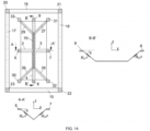
- FIG 14 shows yet another embodiment.
- This sensor according to the invention comprises a groove in the shape of an elongated inverted pyramid, having a rib at the top instead of a tip.
- Slanted resistive paths are provided on the sidewalls and along the slanted ribs of the pyramid, in the same manner and numbered with the same numerical references as for the embodiment of Figure 7 .
- planar resistive paths 15-18 are provided in the vicinity of the cavity.
- an area 70 comprising the elongated upper rib of the pyramid is subjected to silicidation, so that this area represents an essentially zero resistance. This allows to maintain all the formulas as described above for the pyramid with a tip.
- contacts could be provided in the middle (i.e. the common area of resistive paths 2 and 3) and at the outer ends (common areas of resistive paths 29,5,27 and 26,4,28) of the elongated upper rib.
- the inverted elongated pyramid-shaped cavity of Figure 14 is once again equivalently embodied by a positive elongated pyramid extending out from the substrate with resistive paths on the sidewalls and along the slanted ribs of the pyramid.
- a sensor of the invention may comprise multiple cavities or equivalent positive 3D shapes oriented at different angles in the xy plane and provided with slanted resistive paths and planar resistive paths as described above.
- multiple elongated grooves like the ones shown in Figures 13 and 14 may be provided with longitudinal axes oriented in the plane of the drawing at mutual angles different from 90°.
- the additional orientations may be required for deriving independent equations that allow to determine the normal stress components ⁇ xx , ⁇ yy and ⁇ zz in a temperature-compensated way.
- a second groove may be provided at 45° to the first.
- the orientation of the slanted resistive paths relative to the slanted sidewalls of the cavities, prisms or pyramids is not limited to the above-shown examples.
- the slanted resistive paths 2 to 5 need not necessarily run between the middle of the sides of the ground plane of the pyramid and the tip area 11.
- slanted resistive paths do not run from the edge of the cavity to the bottom, but only run along a portion of a slanted sidewall.
- the resistive paths can be produced by implanting portions of the substrate with dopant elements having one of two opposite polarity types, commonly referred to as p-type or n-type dopants.
- the coefficients of the piezo-resistive matrix used in the expression (1) are different for n-type and for p-type resistors.
- the slanted resistors R xz and R yz are preferably produced in p-type silicon because the ⁇ 44 coefficient is very small for an n-type resistor, leading to an inaccurate determination of ⁇ xz from equations (5) and (6).
- the set of equations (17)(18)(21) is preferably based on n-type resistors.
- the sensor of the invention may comprise two versions of any of the above-described designs, one with p-type resistors and one with n-type resistors. Alternatively, the sensor may comprise both polarity types in a single design.
- Figure 15 shows an example of the latter case for determining all the stress components.
- Planar p-type as well as n-type resistors are provided around a single cavity, preferably matched on opposite sides of the cavity.
- P-type resistive paths are indicated by ⁇ +' signs and n-type are indicated by '-' signs in the drawing.
- the slanted resistors on the side walls are p-type while the slanted resistors along the ribs of the pyramid are n-type.
Landscapes
- Physics & Mathematics (AREA)
- General Physics & Mathematics (AREA)
- Engineering & Computer Science (AREA)
- Manufacturing & Machinery (AREA)
- High Energy & Nuclear Physics (AREA)
- Computer Hardware Design (AREA)
- Microelectronics & Electronic Packaging (AREA)
- Power Engineering (AREA)
- Health & Medical Sciences (AREA)
- Toxicology (AREA)
- Condensed Matter Physics & Semiconductors (AREA)
- Pressure Sensors (AREA)
Description
- The present invention is related to a stress sensor integrated in a semiconductor component such as an integrated circuit chip.
- Mechanical stress can be detrimental for the operation of integrated circuits and other semiconductor components. Packaging induced stress is known to affect significantly the performance of transistors and circuits. Similarly, 3D interconnects such as TSVs are known to introduce stress in the active regions of the wafer. It is therefore necessary to evaluate the stress in terms of the stress components of the stress tensor which consists of three normal components σxx, σyy and σzz and three shear components σxz, σyz and σxy, defined with respect to orthogonal directions x, y and z with the xy plane corresponding to the plane of the semiconductor wafer from which the IC or other component is fabricated.
- A well-known approach to detecting package-induced stress is based on the piezoresistive effect in diffused resistors or transistors. One example of a piezo-resistive stress sensor built on this principle is the rosette sensor described in detail in document "Silicon piezoresistive stress sensors and their application in electronic packaging," Suhling and Jaeger, IEEE Sensors Journal, vol. 1, no. 1, pp. 14-30, June 2001. The shift in resistance of complementary type diffused resistors oriented along different directions is monitored to deduce the stress present in the active material. To compensate for the impact of temperature variations during measurements, these resistance shifts must be subtracted one from the other so as to cancel the impact of thermal effects on resistors. These types of sensors however suffer from 3 main limitations. Firstly, they are not sensitive to out-of-plane shear stress components on a (100) wafer surface, which is the one commonly employed for CMOS technology. Secondly, the resistor sensitivity to σzz does not change with a planar rotation of the sensor on a (100) surface, so its contribution is regularly cancelled out with the one from the temperature. Thirdly, it is only possible to extract the difference (σxx - σyy) and not the two components σxx and σyy individually, once again due to the need to compensate for temperature.
- To determine the remaining coefficients (σxz, σyz, σzz and (σxx+σyy)), one approach is to build rosette sensors on a (111) surface, where the transformed piezoresistive matrix provides more orientation-dependent coefficients. Therefore, variations of resistances oriented in different directions due to stress have the potential to provide an independent family of linear equations from which the stress components can be extracted. Nonetheless, the in-plane resistivity matrix being symmetric, it features only 3 independent components. Any in-plane rotation of the resistor can only result in a combination of these three coefficients. Thus at most 3 independent equations can be extracted from a single-polarity rosette sensor, and one is inevitably lost for temperature compensation. In any case, all the sensors based on a (111) surface cannot be processed in conventional CMOS technology where the wafer surface is oriented along the (100) direction.
- Another solution reported in literature is to create a non-planar current on a (100) oriented wafer, as illustrated by documents : "Towards piezo-resistive CMOS sensors for out-of-plane stress", Lemke et al, Proceedings, IEEE 22nd International Conference on Micro Electro Mechanical Systems, March 2009 and "Piezoresistive CMOS sensors for out-of-plane shear stress", Baumann et al, Proceedings IEEE Sensors Conference, 2009. In these sensor designs, the current is forced below a shallow trench isolation (similarly to an STI diode), which makes it non-planar. This principle can be used to detect both σzz and the out-of-plane shear stress σxz and σyz. However the extraction of the σzz , σxz and σyz is very challenging. Indeed, a large part of the current trajectory (below the spacer) is non-vertical. As a result, the structure must be repeated with different STI widths to de-embed σzz from all the others as explained in the above-identified reference by Lemke et al. In the pseudo-Hall sensor used in the above-identified reference by Baumann et al, no solution is proposed to de-embed between the contribution of σxz (vertical current on the sidewalls of the STI) and σxy (horizontal current under the STI).
- V-groove stress sensors are a well-known technique used in the MEMS industry to fabricate sensors. In particular, it has also been used to build membrane sensors that can detect a pressure applied by an external force on the chip. However in that case the V-groove is used simply to build a mechanical structure. The electrical characteristics of the resulting slanted surfaces are not exploited. For example in document
US6150681 , the piezoresistive sensors are put on the membrane and not on the slanted surfaces themselves. Furthermore, all piezoresistive sensors relying on a free membrane or an internal cavity are not suitable for detecting packaging-induced stress precisely because they are sensitive to the external stress (which they are meant to detect).
DocumentFR2950427
DocumentWO02/44655
DocumentUS2009/282930 is related to a force sensor including a polymeric substrate including a cavity with a tilt plane, at least two metal piezoresistors on the tilt plane, and a contact pad connected to the metal piezoresistors. The tilt plane may include a measured interface of from 15° to 75°.
DocumentUS2015/059486 is related to a pressure sensor including an elastic thin film including a first surface and a second surface that face each other, the elastic thin film including an elastomer material, a plurality of protruding deformable structures patterned on the first surface, a piezoresistive electrode formed along surfaces of the plurality of protruding deformable structures and a counter electrode disposed to face the piezoresistive electrode.
DocumentEP1380825 is related to a micromechanical pressure sensor having a part silicon semiconductor frame holding a membrane with stress dependent Wheatstone bridge and compensation bridge piezo resistances having part linear and part quadratic responses on the membrane and others optionally on the frame. - The invention is related to a sensor and to a semiconductor component in accordance with the appended claims. The sensor of the invention is configured to be incorporated in a semiconductor component such as an integrated circuit chip. The component comprises a semiconductor substrate, the substrate originating from the semiconductor wafer onto which a plurality of chips are built. A stress sensor according to the present invention comprises one or more slanted surfaces of the semiconductor substrate material with a known oblique inclination angle relative to the main surface of the substrate, and resistive paths at least on the slanted surfaces. According to a preferred embodiment, two slanted surfaces are provided with complementary inclination angles relative to the main surface, and one or more pairs of resistive paths are produced on the pair of surfaces, the inclination angles of the paths of each pair being equally complementary. The knowledge of the inclination angle allows to determine the out-of-plane stress components based on a measurement of the resistance of the slanted resistive paths. The sensor may comprise a cavity open to the main surface, or a 3D shape on the main surface, and a number of resistive paths on the slanted sidewalls of the cavity or 3D-shape, as well as a number of contacts and terminals for accessing said resistive paths. According to preferred embodiments, the sensor further comprises planar resistive paths in the vicinity of the cavity or 3D shape, which allow to determine the normal stress components, as well as the in-plane shear stress.
- The sensor according to the invention provides a way of monitoring or determining the out-of-plane shear stress that is technically straightforward and reliable in comparison with the existing approaches referred to above.
- The invention is firstly related to a sensor for monitoring and/or measuring stress in the semiconductor component, the stress sensor comprising a substrate formed of a piezoresistive semiconductor material, the substrate comprising a planar main surface, the sensor comprising :
- at least one slanted surface of the substrate material, the slanted surface being defined by an oblique inclination angle with respect to the main surface of the substrate,
- at least one straight resistive path extending on at least part of the slanted surface. The straight resistive path is thus also oriented at an oblique inclination angle relative to the main surface of the substrate. Said angle can be the same angle as the angle of the slanted surface, or it can differ from said angle. According to a preferred embodiment, the inclination angle between the resistive path and the main surface is between 20° and 70°.
- a plurality of contacts and terminals for accessing the slanted resistive path, thereby allowing to measure the electrical resistance of the resistive path and to derive therefrom an assessment of the shear stress in a plane that is not parallel to the main surface of the substrate.
- According to the invention, the sensor comprises at least one pair of slanted surfaces having complementary inclination angles relative to the main surface, and comprising at least one pair of resistive paths which lie in a first plane, the first path on the first slanted surface and the second path on the second slanted surface, wherein the pair of slanted resistive paths also have complementary inclination angles relative to the main surface, and wherein the sensor is configured to measure the shear stress in the first plane defined by the pair of resistive paths.
- The sensor may comprise two of said pairs of slanted surfaces and slanted resistive paths, and be configured to measure the shear stress in a first and second plane, said planes being two mutually non-parallel planes, preferably two mutually orthogonal planes.
- According to an embodiment, the sensor further comprises a plurality of planar resistive paths parallel to the plane of the main surface of the substrate and located in the vicinity of the slanted resistive paths, as well as a plurality of contacts and terminals for accessing the planar resistive paths, thereby allowing to measure the electrical resistance of the planar paths and to derive therefrom an assessment of one or more additional stress components.
- According to embodiments of the invention, the one or more slanted surfaces are the slanted sidewalls of one or more cavities which are open to the main surface of the substrate or to another surface of the substrate and/or the slanted surfaces are the slanted sidewalls of 3-dimensional shapes extending outward from the main surface of the substrate or from another surface of the substrate.
- According to an embodiment, the sensor comprises :
- a cavity or a 3D shape having the shape of a 4-walled pyramid or a frustum of a 4-walled pyramid, comprising a rectangular or square base, a centrally located tip area, four slanted walls extending respectively between the four edges of the base and the tip area, said four walls forming two pairs of slanted surfaces, the surfaces of each pair having complementary inclination angles relative to the main surface of the substrate, and four slanted ribs extending respectively between the corners of the base and the tip area,
- four electrical contacts. According to an embodiment, these contacts are placed along the edges of the base of the pyramid, preferably in the midpoint of said edges. In the latter case, the inclination angle between the four paths and the substrate main surface is essentially the same as the inclination angle of the respective slanted surfaces of the pyramid.
- four slanted resistive paths respectively on the four slanted surfaces, the four paths extending between the tip area and the four electrical contacts, the paths on opposite surfaces having complementary inclination angles relative to the main surface of the substrate.
- The sensor according to the previous paragraph may further comprise a fifth electrical contact located in the tip area, the four resistive paths extending respectively between the four contacts and the fifth contact. Alternatively, the four slanted resistive paths merge in the tip area and the slanted resistive paths on opposing walls of the cavity or the 3D shape are matched in terms of their electric resistance.
- The sensor comprising a pyramid-shaped cavity or 3D shape as described above may further comprise :
- two planar resistive paths in the vicinity of the cavity or the 3D shape, the two planar paths running along perpendicular lines in the plane of the main surface of the substrate,
- electrical contacts at the start and end location of each planar resistive path, and terminals for accessing said contacts,
- four additional electrical contacts placed around the cavity or the 3D shape, one on each of the four corners of the cavity or the 3D shape, and terminals for accessing the corner contacts,
- four slanted resistive paths, each path running along one of the ribs of the cavity or the 3D shape, between the respective corner contacts and the tip area of the cavity or the 3D shape.
- The sensor according to the preceding paragraph may further comprise two additional planar resistive paths, as well as contacts at the start and end location of each additional planar path, wherein :
- the two additional planar paths run parallel respectively to the two perpendicular planar paths,
- the two additional planar paths run on the opposite side of the cavity or the 3D shape with respect to the respective perpendicular planar paths,
- Each pair of parallel planar resistive paths is matched in terms of their electrical resistance.
- The two pairs of parallel resistive paths may form the side edges of a rectangle, with four contacts placed on the corners of the rectangle.
- The sensor comprising a pyramid-shaped cavity or 3D shape may further comprise :
- two planar resistive paths in the vicinity of the cavity or the 3D shape, the two planar paths running along perpendicular lines in the plane of the main surface of the substrate,
- contacts at the start and end location of each planar resistive path, and terminals for accessing said contacts,
- a second cavity or 3D shape of the same shape as the first cavity or 3D shape, and placed in close proximity to the first cavity or 3D shape,
- four contacts placed around the second cavity or 3D shape, on the four corners of the second cavity or 3D shape, and terminals for allowing access to the corner contacts,
- four slanted resistive paths, each path running along the ribs of the second cavity or 3D shape, between the respective corner contacts and the tip area of the second cavity or 3D shape.
- According to an embodiment, the substrate material is a crystalline semiconductor material, and the inclination angles are defined by the crystallographic structure of the material.
- According to an embodiment, the sensor comprises multiple resistive paths obtained by implantation of dopant elements in narrow areas of the slanted surfaces, and, if applicable, in narrow areas of the main surface of the substrate or a surface parallel thereto, and wherein the sensor comprises resistive paths formed by implantation of dopant elements of a first polarity type, as well as resistive paths formed by implantation of dopant elements of a second polarity type, opposite to the first.
- The invention is equally relatedt to a semiconductor component comprising a stress sensor in accordance with the invention.
-
-
Figure 1 illustrates the principle of a sensor according to the invention, including at least one slanted surface at an oblique angle relative to a main surface of a substrate, with a resistive path on the slanted surface. -
Figure 2 illustrates a preferred embodiment of the sensor, comprising slanted surfaces having complementary angles relative to the main surface of the substrate. -
Figure 3 illustrates another embodiment, wherein the slanted surfaces are formed in a vertical sidewall of a recess produced in the substrate. -
Figure 4 shows a top view and cross section views of a stress sensor according to an embodiment of the invention that allows to measure the out-of-plane stress components σxz and σyz.Figure 1 also illustrates the orientation of the crystallographic axes and of the sensor axes for a sensor produced in a (100) silicon wafer. -
Figure 5 shows the sensor ofFigure 4 , but without a contact at the bottom of the cavity. -
Figure 6a & 6b illustrates how to measure the out-of-plane resistance shift in a stress sensor according toFigure 5 . -
Figure 7 illustrates an embodiment of a sensor design according to the invention configured to measure all stress components in a temperature compensated way. -
Figure 8 shows a measurement setup for measuring a resistance shift in a sensor according toFigure 6 or7 . -
Figure 9 shows a compact sensor design according to the invention configured to measure all stress components in a temperature compensated way. -
Figure 10 shows another possible sensor design according to the invention. -
Figure 11 shows a sensor design according to the invention with separate planar resistive paths around a pyramid-shaped cavity. -
Figure 12 illustrates a sensor according to the invention provided with a 3D pyramid extending outward from the substrate. -
Figures 13a and13b show embodiments of a sensor according to the invention, comprising a set of two V-shaped grooves oriented at 90°. -
Figure 14 shows an embodiment comprising a cavity in the shape of an elongated pyramid. -
Figure 15 shows an embodiment comprising resistive paths defined by p-type and n-type implants. - According to the invention, a stress sensor is formed on a semiconductor substrate having a planar main surface, wherein the sensor comprises at least one slanted surface of the substrate material, 'slanted' meaning that the surface is a flat surface oriented at an oblique angle relative to the main surface, and on said slanted surface at least one resistive path. The semiconductor material is preferably a piezoresistive material, more preferably a piezoresistive crystalline material, for example silicon, germanium or a compound semiconductor (e.g. GaAs). The path is slanted as a consequence of the oblique inclination angle of the surface. A 'resistive path' is defined within the present context as a portion of the surface that is equivalent to a one-dimensional conductor and which is thus characterised by a measurable electrical resistance. As the resistive path is one-dimensional, it has a well-defined inclination angle relative to the main surface of the substrate. The resistive path is thus straight relative to the slanted surface. Any oblique (i.e. different from 90°) inclination angle may be applied between the resistive path and the main surface of the substrate. According to a preferred embodiment, the angle is between 20° and 70°.
-
Figure 1a shows an embodiment of a sensor comprising asubstrate 50 withmain surface 100 oriented horizontally and comprising agroove 101 having one slantedsurface 102 defined by oblique angle θ relative to the main surface, with threeresistive paths 103 to 105 on the slanted surface. One path would be enough but three are shown to illustrate different possible orientations of the paths.Figure 1b shows an equivalent embodiment wherein a 3D shape 101' formed of the substrate material extends outwards from themain surface 100 of thesubstrate 50, the 3D shape having one slanted surface 102' with three resistive paths 103'-105' on the slanted surface. It is seen that the inclination angle of the paths may be equal to the inclination angle θ of the surface (paths 103 and 103') or differ from said angle θ (paths 104/105 and 104'/105'). In the embodiment shown, the paths extend between a first and second contact A and B (a contact may be provided only on one side of the path in specific embodiments, see further). The paths and contacts can be produced according to known techniques. The paths are preferably produced by dopant implantation steps in narrow areas of the slanted surface. The contacts can be metal contacts formed in accordance with known semiconductor process technology. - Contacts A and B are accessible through electrical circuitry in the sensor (not shown) and through one or more terminals connected to said circuitry, in any manner known in the art of similar pressure sensors comprising resistive paths on the main surface of a substrate, of which examples are cited in the introductory paragraph. The sensor shown in
Figures 1a or 1b is distinguished from these prior art sensors by the presence of a slanted resistive path. Through the contacts and terminals, the resistance of the paths can be measured. Changes in the resistance values are proportional to changes in the out-of-plane shear stress component in the vertical planes P1, P2, P3 perpendicular to the main surface. By monitoring the resistance of these paths, the sensor allows the monitoring of changes in the out-of-plane components of the shear stress occurring in the substrate in these planes. The actual measurement of the numerical value of the out-of-plane shear stress components defined in a particular 3-dimensional coordinate system requires the presence of additional sensors or additional resistive paths as will be described further in this description. - According to an embodiment illustrated in
Figure 2 , agroove 110 is provided in themain surface 100 having two slantedsurfaces main surface 100. Or in other words, the two slanted surfaces are symmetrically opposed relative to asymmetry plane 113 that is perpendicular to themain surface 100. Two resistive paths R1,R2 are formed respectively on these slanted surfaces, so that the resistive paths also have complementary inclination angles relative to the main surface. The resistive paths R1, R2 are located in a plane that is not parallel to themain surface 100. The embodiment ofFigure 2 comprises several pairs R1, R2 which answer to that specification. The two resistors are located in the same plane. In the example shown, this plane is perpendicular to themain surface 100, but the paths R1,R2 may equally be located in a plane that is non-perpendicular and non-parallel relative to the main surface. Instead of on the slanted surfaces of agroove 110, the resistive paths R1,R2 may be formed on the slanted surfaces of a 3D-shape formed of the substrate material and extending outward from the main surface and having sidewalls with complementary inclination angles. - The grooves 101,110 described above are examples of cavities which are open to the
main surface 100 of the substrate. The 3D shapes 101' described above are formed directly on said main surface. According to other embodiments, a groove is formed that is open to a surface that is not parallel to the main surface, or a 3D shape may be formed on such a surface. An example of such an embodiment is shownFigure 3 , where agroove 120 is formed in a sidewall of arecess 121 formed in themain surface 100 of thesubstrate 50. Thegroove 120 is thereby open to thesidewall surface 122. The resistive paths R1 ,R2 are again formed on the slanted surfaces which form the sidewalls of thegroove 120. The slanted surfaces have complementary inclination angles θ and 180°- θ relative to themain surface 100. In this case, this means that the surfaces are symmetrically opposed relative to ahorizontal symmetry plane 123. One way of producing the resistive paths in this case would be to deposit a doped oxide (e.g PSG, phosphosilicate glass) to fill thecavity 120, then pattern it with an anisotropic etch featuring sufficient underlap so as to keep only the doped oxide near the buried path on which the resistive path is to be created. Finally, an anneal would allow the dopants contained in the doped oxide to transfer to the neighboring silicon, and then the remaining doped oxide can be removed isotropically (e.g wet etch). - A pair of resistive paths R1,R2 as described above, with well-defined complementary inclination angles relative to the
main surface 100, allows to determine the numerical value of the out-of-plane shear stress component in the plane defined by the two paths R1,R2. This will be demonstrated for the specific case of a pyramid-shaped cavity, but the mathematics is the same for any of the pairs R1,R2 referred to above. According to particular embodiments, also illustrated hereafter, the resistors R1, R2 are matched, i.e. R1 = R2. -
Figure 4 illustrates an embodiment of a sensor according to the invention, comprising a pyramid-shapedcavity 1 that is open to themain surface 100 of thesubstrate 50. The pyramid-shapedcavity 1 is preferably produced by an anisotropic etch process, performed on acrystalline semiconductor wafer 50 with a pre-defined crystallographic orientation. Most silicon wafers used in the semiconductor industry have their flat surface oriented in the (100) plane of the silicon crystallographic structure. It is known in the art that this configuration allows to produce a pyramid-shaped cavity by anisotropic wet etching, e.g. KOH-based, in a square portion of the wafer, the remainder being protected by a hardmask or resist layer. The etching process aligns on the crystallographic axes to thereby form a cavity with well-defined inclination angles of the cavity walls. The cavity may have dimensions in the order of nanometers; for example the sides of the pyramid's ground plane may be approximately 400nm long. - In the sensor of
Figure 4 ,resistive paths contacts central contact 10 in thetip area 11 of the cavity. Preferably thecontact 10 is produced on a flat portion of said tip area, i.e. the inverted pyramid is in fact a flattened pyramid also known as a frustum of a pyramid, i.e. a pyramid with a top portion chopped off along a plane parallel to the ground plane. The fourresistive paths 2 to 5 are equivalent to 4 resistors : two resistors Rx1 and Rx2 in the xz plane and two resistors Ry1 and Ry2 in the yz plane. The angle θ is known. Opposed slanted surfaces are symmetrical with respect to a plane perpendicular to thesubstrate 50, as expressed by the equal angles 90°-θ in both the xz plane and the yz plane. In the case of a cavity produced by wet etching in a crystallographic structure, the angle θ is defined by the crystallographic planes of the semiconductor material into which the pyramid has been created. The sensor further comprises terminals (not shown) on the exterior of the chip which are connected via circuitry within the chip to therespective contacts 6 to 10, so that each of these contacts can be individually accessed, for example for connecting them to a voltage source or to ground. According to an embodiment, one terminal is provided for each contact and individually connected to its respective contact. Alternatively the number of terminals may be lower than the number of contacts, and the measurements may be performed in a time-multiplexed manner. - In a coordinate system that is aligned with the crystallographic axes of a crystalline substrate material, the relation between the stress tensor in the substrate and the normalized resistance shifts in the direction of the stress components is the following :

- The axes x, y and z in
Figure 4 are normally not aligned with the crystallographic axes of the substrate material. The relation between the resistance shifts defined in x, y and z can however be determined on the basis of the equations (1) and the orientation of the axes x, y and z with respect to the crystallographic axes. For example, if the substrate is a (100) silicon substrate as illustrated in the insert inFigure 4 , the crystallographic axes in the plane of the wafer are oriented along the [100] and [010] directions. The cavity is produced according to these directions, hence the x and y directions ofFigure 4 correspond to the [110] and [1 10] directions. - When a stress is applied to the substrate onto which the sensor of
Figure 4 is built, at a time when the substrate is in a theoretical 'zero-stress' condition, the resistances Rx1 and Rx2 shift over values ΔRx1 and ΔRx2. The relation between the normalized shifts :


- The measurement of the resistance shifts may be done by applying a known voltage difference between the
central contact 10 and therespective side contacts 6 to 9 of the sensor, and measuring the current. This is done once for a reference condition chosen to closely approximate the theoretical zero stress condition. The measurement of stress is therefore always a relative measurement of the stress with respect to the reference condition. Such a stress measurement then entails the measurement of the resistance values under test conditions. The values of ΔRx1, ΔRx2, ΔRy1 and ΔRy2 are calculated as the difference between the measured resistances and the resistances obtained at the reference condition. Preferably, the opposing slanted resistive paths are matched at the reference condition, i.e. Rx1 = Rx2 = R0x and Ry1 = Ry2 = R0y at the reference condition. In that case the following is true :
- A second embodiment is shown in
Figure 5 . In this embodiment, the bottom contact is absent, and theresistive paths 2 to 5 extend between thecontacts 6 to 9 and thecentral tip area 11 of the inverted pyramid, where the resistive paths merge to form a node between the two pairs ofconductors 2+3 and 4+5, i.e. thetip area 11 is part of two intersectingconductive paths 2+3 and 4+5. In this case the shape of the cavity may be a frustum of a pyramid or it may be an actual inverted pyramid with a tip. The measurement of the out-of-plane stress components σxz and σyz is possible with the sensor ofFigure 5 , provided that the opposite slanted resistive paths are matched at the reference condition , i.e. Rx1 = Rx2 = R0x and Ry1 = Ry2 = R0y. - One way of measuring δRx1 - δRx2 with this sensor is illustrated in
Figure 6a . The measured voltage of this measurement setup is Vr :


- Hence the final expression:

Figure 6b illustrates the analogue setup for measuring δRy1 - δRy2. - A further preferred embodiment of a stress sensor according to the invention is configured to measure not only the out-of-plane shear stress components σxz and σyz but additionally the normal stress components σxx, σyy and σzz in a temperature-compensated way. A first possible realization of this embodiment is shown in
Figure 7 . The sensor comprises additional planarresistive paths 15 to 18 in the vicinity of the inverted pyramid-shapedcavity 1, term 'planar path' distinguishing these paths from the `slanted paths', and indicating that the resistive paths are parallel to the plane of themain surface 100 of thesubstrate 50. Preferably the planar paths are located on saidmain surface 100. These paths are obtainable by implanting dopants in delimited areas of thesubstrate surface 100, in a manner known in the art, for example for the production of currently known stress sensors referred to in the introductory section. Each path is equivalent to a planar resistor. The embodiment ofFigure 7 has a symmetrical layout, with planar resistors Rx1 f and Rx2 f placed on opposite sides of the pyramid and oriented in the x-direction, and planar resistors Ry1 f and Ry2 f placed on opposite sides of the pyramid and oriented in the y-direction. The planar resistors are preferably matched : Rx1 f = Rx2 f and Ry1 f = Ry2 f. The four planar resistors are accessible through fourcontacts 20 to 23, i.e. the planar resistors form a rectangle with the four contacts placed on the corners. The slanted resistors already described in relation toFigures 4 to 6 are now named Rx1 g , Rx2 g , Ry1 g and Ry2 g to distinguish them from the planar resistors. The slanted resistors are matched, i.e. Rx1 9 = Rx2 g and Ry1 9 = Ry2 9. In this embodiment, there is no contact at the bottom of the pyramid (but it could be present according to an alternative embodiment). - In addition, a second pyramid-shaped
cavity 25 is provided in close proximity to thefirst cavity 1 so that the stress state of the substrate is essentially the same at the locations of the twocavities second pyramid 25 has slantedresistive paths 26 to 29 along the ribs of the pyramid, equivalent to resistors Ru1 g , Ru2 g , Rv1 g and Rv2 g. These latter resistors are located in the uz and vz planes of a rotated axis system uvz, which is rotated 45° about the z-axis with respect to x and y. These resistors are equally preferably matched : Ru1 g = Ru2 g and Rv1 g = Rv2 g.Contacts 30 to 33 are provided on the four corners of thecavity 25, connected to terminals (not shown) for accessing these contacts individually. In addition, preferably matched planarresistive paths 35 to 38 are produced along the u and v directions, equivalent respectively to four planar resistors : Ru1 f = Ru2 f and Rv1 f = Rv2 f. Four contacts 39-42 are provided so that the planar paths 35-38 form a rectangle with the contacts 39-42 at the four corners. - On the basis of resistance measurements performed on this sensor design, it is possible to derive three independent and temperature-compensated equations, from which to solve σxx, σyy and σzz. The normalized shift of the sum Rx1 g + Rx2 g is defined as δRxx g :


first pyramid 1 with respect to the crystallographic axes of the substrate. In the case of a (100) silicon substrate, wherein the x-axis is oriented in the [110] direction (seeFigure 4 ), this relation is :


- Reference is again made to the Suhling and Jaeger article referred to above for more details about how these formulas are obtained. The substitution of formulas (10) and (11) in formula (9) results in the following relation:


Figure 7 , the resistances Rxx f and Ryy f are preferably defined as :


Equations (12) to (15) together form a system of four equations :
- The coefficients Af, Bf, Cf, Ag, Bg and Cg can be calculated on the basis of the above-described formulas. Alternatively, the coefficients can be obtained by a calibration. Known calibration techniques can be employed wherein pre-defined stress components are applied. For in-plane normal stress components (σxx and σyy), a 4 point bending tool can be used, as well-known in the art. Although the 4 point bending cannot create shear stress alone (σxy), it is possible to use a rotated die (rotated about the z-axis) where the 4 point bending system will create all components (σxx, σyy, and σxy), in the coordinate system of the sensor (i.e. x and y refer here to the sensor axes and not the 4pt bending tool axes). But the contributions from (σxx , σyy) can be determined thanks to the first set of calibrations, which allows to extract the sensitivity to σxy. For σzz, a nano-indenter tool can be used, as described for example in document "Towards piezo-resistive CMOS sensors for out-of-plane stress", Lemke et al, Proceedings, IEEE 22nd International Conference on Micro Electro Mechanical Systems, March 2009. Finally, for σxz and σyz, a microbump can be processed on top of the sensor and a shear test of the microbump can apply either σxz and σyz.
- The 4
X 4 matrix in the system of equations (16) is a singular matrix, so the system cannot be solved unless one additional equation is provided. The following two equations are directly derived from the system (16):

second pyramid 25. Ru g is defined as Ru1 g+Ru2 g and Rv g is defined as Rv1 g+Rv2 g . For symmetry reasons, the sum Ru g+Rv g has the following sensitivity to stress:


pyramid 25 with respect to the axis z (seeFig. 4 ). The difference between equations (19) and (20) yields :
- From the linearly independent equations (17), (18) and (21), the stress components σxx, σyy and σzz can then be calculated, after a measurement of δRxx f, δRxx g, δRyy f, δRyy g, δRuv g and δRuv f. The measurements of these resistance shifts can be done by measuring the respective resistances by coupling the relevant contacts to a voltage source and measuring the resulting current, as illustrated in
Figure 8 for the exemplary case of measuring Ryy g. The δ-values can be obtained by subtracting the known resistance value at the reference condition close to the theoretical zero-stress condition, from the measured value. The known resistances at the reference condition can be obtained from a calibration measurement. Advantageously, additional matching may simplify the measurements. For example according to a preferred embodiment, the resistances Rxx g and Rxx f are matched, i.e. Rxx g = Rx1 g+Rx2 g = Rxx f = Rx1 f+Rx2 f = Rx0 at the reference condition. In this case, the left hand side of equation (17) can be found from a measurement of Rxx f - Rxx g and the knowledge of Rx0. - The embodiment of
Figure 7 further allows to measure σxy from the planar resistances arranged in a rectangular pattern with four contacts 20-23 at the corners of the rectangle. This is the known design of a pseudo-Hall sensor, allowing to measure σxy directly. The pseudo-Hall sensor is described for example in "A novel stress sensor based on the transverse pseudo-Hall effect of MOSFETs,", M. Doelle et al, Micro Electro Mechanical Systems, 2003. MEMS-03 Kyoto. IEEE The Sixteenth Annual International Conference on, 2003, pp. 490-493. The sensor ofFigure 7 thus allows to measure all six components of the stress tensor. - In
Figure 7 , the resistive paths 35-38 could be omitted. The values of Ru1 f, Ru2 f, Rv1 f and Rv2 f can also be derived from Rx1 f, Rx2 f, Ry1 f and Ry2 f taking into account the orientation of u and v with respect to x and y and taking into account the piezo-resistive matrix. This calculation is explained for example in the Suhling and Jaeger article referred to above. -
Figure 9 shows another embodiment, comprising asingle cavity 1, and wherein slantedresistive paths 2 to 5 and 26 to 29 as described above are formed both along the sidewalls of the cavity and along the ribs, with 8 contacts formed around the cavity : fourcontacts 6 to 9 in the middle of the cavity's edges and fouradditional contacts 30 to 33 on the corners of the cavity. The fourplanar resistors 15 to 18 arranged in a rectangle are equally present in this embodiment. The values of planar resistors Ru1 f, Ru2 f, Rv1 f and Rv2 f in the u and v directions can be calculated from the planar resistors in the x and y directions, taking into account the known orientation of u and v with respect to x and y and the piezo-resistive matrix. Alternatively, four additional planar resistors arranged in the u and v directions can be added to the design ofFigure 9 , allowing the direct measurement of Ru1 f, Ru2 f, Rv1 f and Rv2 f. σxy can be obtained by using the planar rectangle oriented along the x and y axes as a pseudo-Hall sensor. In this way, the sensor ofFigure 9 is a more compact version of a sensor according to the invention that allows to measure all six stress components. -
Figure 10 shows another alternative, comprising only one planar resistor Rx f in the x-direction and one planar resistor Ry f in the y direction. A stated above, the presence of matched planar resistors on opposite sides of the pyramid is not required for determining the system of equations (17)(18)(21). So the sensor ofFigure 10 is capable of sensing the stress components σxz, σyz, σxx, σyy and σzz. The in-plane shear stress σxy cannot be measured by this sensor. -
Figure 11 shows another variation that allows to measure all stress components apart from σxy. It is seen that the planarresistive paths 15 to 18 do not form a closed rectangle in this embodiment, but are formed of separated resistive paths, each having a pair ofdedicated contacts 20a/21a; 20b/23b;21b/22b;23a/22a. - The invention is not limited to embodiments which include a pyramid-shaped cavity. The same equations can be derived from a positive pyramid 1' extending outward from the surface of the
substrate 50 and formed of the substrate material, as illustrated inFigure 12 . The pyramid 1' is the 'positive' of the cavity shown inFigure 4 . What is important is that the angle θ of inclination of the pyramid's sidewalls is known and that resistive paths are produced on the sidewalls, preferably combined with planar resistive paths in the vicinity of the pyramid. A positive pyramid can be obtained by etching two adjacent V-shaped grooves, in two orthogonal directions. All the above-described embodiments are valid when the pyramid-shapedcavities - Another alternative is illustrated in
Figure 13a . This sensor comprises two mutually perpendicular V-shapedgrooves resistive paths contacts Figure 13a . A contact could furthermore be present at the bottom of the grooves, but when this is not the case as in the embodiment shown inFigure 13a , the slanted paths have matched resistances : Rx1 = Rx2 and Ry1 = Ry2. With the angle θ known, it is clear that this sensor design is equivalent to the design ofFigure 5 in terms of determining the out-of-plane shear stress components σxz and σyz. Instead of the two grooves ofFigure 13a , two mutually perpendicular prisms extending outward from the substrate, with triangular cross-sections identical to the cross-sections of thegrooves - In
Figure 13b , the same grooves are shown, but the first one further comprises slanted resistive paths oriented at 45° relative to thepaths resistors Figures 7 and9 to 11 , namely the paths oriented along the ribs of the pyramid-shaped cavity. By adding planar resistors to the design ofFigure 13b , a sensor may therefore be obtained that is capable of measureing all six stress components. -
Figure 14 shows yet another embodiment. This sensor according to the invention comprises a groove in the shape of an elongated inverted pyramid, having a rib at the top instead of a tip. Slanted resistive paths are provided on the sidewalls and along the slanted ribs of the pyramid, in the same manner and numbered with the same numerical references as for the embodiment ofFigure 7 . Also in analogy with the latter embodiment, planar resistive paths 15-18 are provided in the vicinity of the cavity. In the embodiment shown, anarea 70 comprising the elongated upper rib of the pyramid is subjected to silicidation, so that this area represents an essentially zero resistance. This allows to maintain all the formulas as described above for the pyramid with a tip. Alternatively, contacts could be provided in the middle (i.e. the common area ofresistive paths 2 and 3) and at the outer ends (common areas ofresistive paths Figure 14 is once again equivalently embodied by a positive elongated pyramid extending out from the substrate with resistive paths on the sidewalls and along the slanted ribs of the pyramid. - A sensor of the invention may comprise multiple cavities or equivalent positive 3D shapes oriented at different angles in the xy plane and provided with slanted resistive paths and planar resistive paths as described above. For example multiple elongated grooves like the ones shown in
Figures 13 and14 may be provided with longitudinal axes oriented in the plane of the drawing at mutual angles different from 90°. The additional orientations may be required for deriving independent equations that allow to determine the normal stress components σxx, σyy and σzz in a temperature-compensated way. For example, instead of providing resistive paths along the ribs of the cavity ofFigure 14 , a second groove may be provided at 45° to the first. - The orientation of the slanted resistive paths relative to the slanted sidewalls of the cavities, prisms or pyramids is not limited to the above-shown examples. In the embodiment of
Figures 4 and5 , for example, the slantedresistive paths 2 to 5 need not necessarily run between the middle of the sides of the ground plane of the pyramid and thetip area 11. According to other embodiments, slanted resistive paths do not run from the edge of the cavity to the bottom, but only run along a portion of a slanted sidewall. These alternatives may influence the complexity of the equations for calculating the out-of-plane and other stress components, but this mathematical procedure of which an example has been give above, remains within the capabilities of the skilled person. The invention is related to the presence of slanted resistive paths configured in a manner which allows the resistance of these paths to be correlated to the stress condition of the sensor. The precise layout of the sensor may differ within the thus-identified framework of the invention. - In any of the embodiments described above, the resistive paths can be produced by implanting portions of the substrate with dopant elements having one of two opposite polarity types, commonly referred to as p-type or n-type dopants. The coefficients of the piezo-resistive matrix used in the expression (1) are different for n-type and for p-type resistors. Although theoretically, all the stress components can be found when all the resistors of the sensor have the same polarity type, in practice it is often preferred to use a combination of p type and n type resistors, because the coefficients of one or the other polarity type lead to a better-defined set of equations. For example, the slanted resistors Rxz and Ryz are preferably produced in p-type silicon because the π44 coefficient is very small for an n-type resistor, leading to an inaccurate determination of σxz from equations (5) and (6). On the other hand, the set of equations (17)(18)(21) is preferably based on n-type resistors. In order to obtain the equations for the optimal choice of resistor type (p or n), the sensor of the invention may comprise two versions of any of the above-described designs, one with p-type resistors and one with n-type resistors. Alternatively, the sensor may comprise both polarity types in a single design.
Figure 15 shows an example of the latter case for determining all the stress components. Planar p-type as well as n-type resistors are provided around a single cavity, preferably matched on opposite sides of the cavity. P-type resistive paths are indicated by `+' signs and n-type are indicated by '-' signs in the drawing. The slanted resistors on the side walls are p-type while the slanted resistors along the ribs of the pyramid are n-type.
Claims (14)
- A stress sensor for monitoring and/or measuring stress in a semiconductor component, the stress sensor comprising a substrate (50) formed of a piezoresistive semiconductor material, the substrate comprising a planar main surface (100), the sensor further comprising:• at least one slanted surface (111,112) of the substrate material, the slanted surface being defined by an oblique inclination angle with respect to the main surface of the substrate,• at least one resistive path (R1, R2) extending on at least part of the slanted surface, wherein the resistive path is straight relative to the slanted surface, and thereby forms a slanted resistive path with respect to the main surface,• a plurality of contacts (6,7,8,9) electrically connected to the at least one slanted resistive path, and terminals for accessing the slanted resistive path, thereby allowing to measure the electrical resistance of the resistive path and to derive therefrom an assessment of the shear stress in a plane that is not parallel to the main surface of the substrate,characterized in that :- the stress sensor comprises at least one pair of said slanted surfaces (111,112) having complementary inclination angles relative to the main surface (100), and comprising at least one pair of said resistive paths (R1,R2) which lie in a first plane, the first path on the first slanted surface and the second path on the second slanted surface, wherein the pair of slanted resistive paths also have complementary inclination angles relative to the main surface (100), and wherein the sensor is configured to measure the shear stress in the first plane defined by the pair of resistive paths.
- The stress sensor according to claim 1, comprising two of said pairs of slanted surfaces and slanted resistive paths (2,3;4,5), and configured to measure the shear stress in a first and second plane, said planes being two mutually non-parallel planes.
- The stress sensor according to any one of the preceding claims, further comprising a plurality of planar resistive paths (15-18) parallel to the plane of the main surface (100) of the substrate (50) and located in the vicinity of the slanted resistive paths, as well as a plurality of contacts (20-23) and terminals for accessing the planar resistive paths, thereby allowing to measure the electrical resistance of the planar paths and to derive therefrom an assessment of one or more additional stress components.
- The stress sensor according to any one of the preceding claims, wherein the one or more slanted surfaces are the slanted sidewalls of one or more cavities (1,101,110) which are open to the main surface (100) of the substrate or to another surface (122) of the substrate and/or wherein the slanted surfaces are the slanted sidewalls of 3-dimensional shapes (1',101') extending outward from the main surface (100) of the substrate or from another surface (122) of the substrate.
- The stress sensor according to claim 4 comprising :• a cavity (1) or a 3D shape (1') having the shape of a 4-walled pyramid or a frustum of a 4-walled pyramid, comprising a rectangular or square base, a centrally located tip area (11), four slanted walls extending respectively between the four edges of the base and the tip area, said four walls forming two pairs of slanted surfaces, the surfaces of each pair having complementary inclination angles relative to the main surface (100) of the substrate, and four slanted ribs extending respectively between the corners of the base and the tip area,• four electrical contacts (6,7,8,9),• four slanted resistive paths respectively on the four slanted surfaces, the four paths extending between the tip area (11) and the four electrical contacts, the paths on opposite surfaces having complementary inclination angles relative to the main surface (100) of the substrate.
- The stress sensor according to claim 5, comprising a fifth electrical contact (10) located in the tip area (11), the four resistive paths (2,3,4,5) extending respectively between the four contacts (6,7,8,9) and the fifth contact (10).
- The stress sensor according to claim 5, wherein the four slanted resistive paths merge in the tip area (11) and wherein the slanted resistive paths on opposing walls of the cavity or the 3D shape are matched in terms of their electric resistance, i.e. the resistances of the resistive paths are equal at a reference condition chosen to closely approximate a theoretical zero stress condition.
- The stress sensor according to any one of claims 5 to 7, further comprising :• two planar resistive paths (15,17) in the vicinity of the cavity or the 3D shape (1,1'), the two planar paths running along perpendicular lines in the plane of the main surface of the substrate,• electrical contacts (23,22,20) at the start and end location of each planar resistive path, and terminals for accessing said contacts,• four additional electrical contacts (30,31,32,33) placed around the cavity or the 3D shape, one on each of the four corners of the cavity or the 3D shape, and terminals for accessing the corner contacts,• four slanted resistive paths (26,27,28,29), each path running along one of the ribs of the cavity or the 3D shape, between the respective corner contacts and the tip area (11) of the cavity or the 3D shape.
- The stress sensor according to claim 8, comprising two additional planar resistive paths (16,18), as well as contacts (20,21,22) at the start and end location of each additional planar path, wherein :• the two additional planar paths (16,18) run parallel respectively to the two perpendicular planar paths (15,17),• the two additional planar paths run on the opposite side of the cavity (1) or the 3D shape (1') with respect to the respective perpendicular planar paths,• Each pair of parallel planar resistive paths is matched in terms of their electrical resistance.
- The stress sensor according to claim 9, wherein the two pairs of parallel resistive paths form the side edges of a rectangle, with four contacts placed on the corners of the rectangle.
- The stress sensor according to any one of claims 8 to 10, further comprising :• two planar resistive paths (15,17) in the vicinity of the cavity or the 3D shape, the two planar paths running along perpendicular lines in the plane of the main surface of the substrate,• contacts (23,22,20) at the start and end location of each planar resistive path, and terminals for accessing said contacts,• a second cavity (25) or 3D shape of the same shape as the first cavity or 3D shape (1,1'), and placed in close proximity to the first cavity (1) or 3D shape,• four contacts (30,31,32,33) placed around the second cavity or 3D shape, on the four corners of the second cavity or 3D shape, and terminals for allowing access to the corner contacts,• four slanted resistive paths (26,27,28,29), each path running along the ribs of the second cavity or 3D shape, between the respective corner contacts and the tip area of the second cavity or 3D shape.
- The stress sensor according to any one of the preceding claims, wherein the substrate material is a crystalline semiconductor material, and wherein the inclination angles are defined by the crystallographic structure of the material.
- The stress sensor according to any one of the preceding claims, comprising multiple resistive paths obtained by implantation of dopant elements in narrow areas of the slanted surfaces, and, if applicable, in narrow areas of the main surface of the substrate or a surface parallel thereto, and wherein the sensor comprises resistive paths formed by implantation of dopant elements of a first polarity type, as well as resistive paths formed by implantation of dopant elements of a second polarity type, opposite to the first.
- A semiconductor component comprising a stresssensor in accordance with any one of the preceding claims.
Priority Applications (3)
| Application Number | Priority Date | Filing Date | Title |
|---|---|---|---|
| EP17189517.0A EP3450947B1 (en) | 2017-09-05 | 2017-09-05 | Stress sensor for semiconductor components |
| JP2018149619A JP7174562B2 (en) | 2017-09-05 | 2018-08-08 | Stress sensor for semiconductor components |
| US16/121,369 US10607901B2 (en) | 2017-09-05 | 2018-09-04 | Stress sensor for semiconductor components |
Applications Claiming Priority (1)
| Application Number | Priority Date | Filing Date | Title |
|---|---|---|---|
| EP17189517.0A EP3450947B1 (en) | 2017-09-05 | 2017-09-05 | Stress sensor for semiconductor components |
Publications (2)
| Publication Number | Publication Date |
|---|---|
| EP3450947A1 EP3450947A1 (en) | 2019-03-06 |
| EP3450947B1 true EP3450947B1 (en) | 2024-01-17 |
Family
ID=59829194
Family Applications (1)
| Application Number | Title | Priority Date | Filing Date |
|---|---|---|---|
| EP17189517.0A Active EP3450947B1 (en) | 2017-09-05 | 2017-09-05 | Stress sensor for semiconductor components |
Country Status (3)
| Country | Link |
|---|---|
| US (1) | US10607901B2 (en) |
| EP (1) | EP3450947B1 (en) |
| JP (1) | JP7174562B2 (en) |
Families Citing this family (5)
| Publication number | Priority date | Publication date | Assignee | Title |
|---|---|---|---|---|
| WO2018086853A1 (en) * | 2016-11-09 | 2018-05-17 | Imec Vzw | Apparatus for combined stem and eds tomography |
| IT201700044301A1 (en) * | 2017-04-21 | 2018-10-21 | St Microelectronics Srl | EFFORT SENSOR FOR THE MONITORING OF THE HEALTH STATUS OF STRUCTURES MADE WHICH CONSTRUCTION, BUILDINGS, INFRASTRUCTURE AND THE LIKE. |
| JP7133763B2 (en) * | 2019-05-09 | 2022-09-09 | 株式会社テック技販 | Load sensor and load detection method |
| US11650110B2 (en) * | 2020-11-04 | 2023-05-16 | Honeywell International Inc. | Rosette piezo-resistive gauge circuit for thermally compensated measurement of full stress tensor |
| CN114112129B (en) * | 2021-11-19 | 2022-08-05 | 苏州纳芯微电子股份有限公司 | Substrate stress sensor and sensing equipment |
Family Cites Families (18)
| Publication number | Priority date | Publication date | Assignee | Title |
|---|---|---|---|---|
| JPS5664472A (en) * | 1979-10-30 | 1981-06-01 | Nec Corp | Detector for strain by semiconductor |
| JPS60154574A (en) * | 1984-01-23 | 1985-08-14 | Fuji Electric Corp Res & Dev Ltd | Sense of pressure sensor |
| JPS6389282A (en) * | 1986-09-30 | 1988-04-20 | 株式会社東芝 | Tactile sensor |
| JPH06130083A (en) * | 1992-04-01 | 1994-05-13 | Nec Corp | Semiconductor acceleration sensor |
| JP3237256B2 (en) * | 1993-01-12 | 2001-12-10 | 株式会社デンソー | Acceleration detection circuit |
| US6150681A (en) | 1998-07-24 | 2000-11-21 | Silicon Microstructures, Inc. | Monolithic flow sensor and pressure sensor |
| JP3368344B2 (en) * | 1998-11-24 | 2003-01-20 | 学校法人立命館 | Semiconductor strain gauge and strain measurement method using the same |
| US6951143B1 (en) * | 2000-11-28 | 2005-10-04 | Michelin Recherche Et Technique S.A. | Three-axis sensor assembly for use in an elastomeric material |
| DE10231727A1 (en) * | 2002-07-13 | 2004-01-22 | Robert Bosch Gmbh | Micromechanical pressure sensor device and corresponding measuring arrangement |
| JP2004340858A (en) * | 2003-05-19 | 2004-12-02 | Sharp Corp | Physical quantity sensor and manufacturing method thereof |
| US7765880B2 (en) * | 2008-05-19 | 2010-08-03 | Hong Kong Polytechnic University | Flexible piezoresistive interfacial shear and normal force sensor and sensor array |
| FR2950427B1 (en) * | 2009-09-21 | 2012-10-12 | Ct Tech Des Ind Mecaniques | DEFORMATION GAUGE IN SELF-POWERED INTEGRATED CIRCUIT |
| CA2806543C (en) * | 2010-11-24 | 2016-05-17 | The Governors Of The University Of Alberta | A novel embedded 3d stress and temperature sensor utilizing silicon doping manipulation |
| KR102081892B1 (en) * | 2013-09-05 | 2020-02-26 | 삼성전자주식회사 | Resistive pressure sensor including piezo-resistive electrode |
| CN104819789B (en) | 2015-02-10 | 2017-05-24 | 华进半导体封装先导技术研发中心有限公司 | Stress sensor and manufacture method thereof |
| WO2018067396A1 (en) * | 2016-10-03 | 2018-04-12 | Flir Systems, Inc. | Methods for routing electrical interconnections and resultant structures |
| US10804115B2 (en) * | 2017-08-03 | 2020-10-13 | General Electric Company | Electronics package with integrated interconnect structure and method of manufacturing thereof |
| TWI695965B (en) * | 2017-12-21 | 2020-06-11 | 愛盛科技股份有限公司 | Magnetic field sensing device |
-
2017
- 2017-09-05 EP EP17189517.0A patent/EP3450947B1/en active Active
-
2018
- 2018-08-08 JP JP2018149619A patent/JP7174562B2/en active Active
- 2018-09-04 US US16/121,369 patent/US10607901B2/en active Active
Also Published As
| Publication number | Publication date |
|---|---|
| US10607901B2 (en) | 2020-03-31 |
| JP7174562B2 (en) | 2022-11-17 |
| EP3450947A1 (en) | 2019-03-06 |
| US20190074231A1 (en) | 2019-03-07 |
| JP2019060855A (en) | 2019-04-18 |
Similar Documents
| Publication | Publication Date | Title |
|---|---|---|
| EP3450947B1 (en) | Stress sensor for semiconductor components | |
| US10775248B2 (en) | MEMS strain gauge sensor and manufacturing method | |
| Kumar et al. | Design principles and considerations for the ‘ideal’silicon piezoresistive pressure sensor: a focused review | |
| US10768064B2 (en) | MEMS pressure gauge sensor and manufacturing method | |
| US11255740B2 (en) | Pressure gauge chip and manufacturing process thereof | |
| US9857247B2 (en) | Method and device for sensing isotropic stress and providing a compensation for the piezo-hall effect | |
| EP0195232B1 (en) | Piezoresistive strain sensing device | |
| JP2575939B2 (en) | Semiconductor acceleration sensor | |
| JP4335545B2 (en) | Sensor for detecting both pressure and acceleration and manufacturing method thereof | |
| Gharib et al. | On the feasibility of a new approach for developing a piezoresistive 3D stress sensing rosette | |
| Lemke et al. | Piezoresistive CMOS sensor for out-of-plane normal stress | |
| US20130205910A1 (en) | Novel embedded 3d stress and temperature sensor utilizing silicon doping manipulation | |
| JP4431475B2 (en) | Semiconductor type 3-axis acceleration sensor | |
| US9857258B2 (en) | Pressure sensor to sense multi-directional movement | |
| US8511170B2 (en) | Pressure transducer having structure for monitoring surface charge | |
| CN111521304B (en) | Micro-pressure sensor chip and preparation method thereof | |
| EP3323778B1 (en) | Mems device and method for calibrating a mems device | |
| US6865951B2 (en) | Semiconductor pressure sensor | |
| EP3056865B1 (en) | Sensor arrangement | |
| JP2011027611A (en) | Semiconductor pressure sensor, and method for manufacturing the same | |
| Mikhailenko et al. | Diagnostics of thermal stress in MEMS pressure transducer based on Tenso-emf Effect | |
| RU2507490C1 (en) | Sensor of absolute pressure of high accuracy based on semiconducting sensitive element with rigid centre | |
| Senturia | A piezoresistive pressure sensor | |
| Niu et al. | The Design and Implementation of High Pressure Rectangular Diaphragm Sensor Based on MEMS Technology | |
| Manook et al. | Numerical study of smart pressure sensors: the piezoMOS effect |
Legal Events
| Date | Code | Title | Description |
|---|---|---|---|
| PUAI | Public reference made under article 153(3) epc to a published international application that has entered the european phase |
Free format text: ORIGINAL CODE: 0009012 |
|
| STAA | Information on the status of an ep patent application or granted ep patent |
Free format text: STATUS: THE APPLICATION HAS BEEN PUBLISHED |
|
| AK | Designated contracting states |
Kind code of ref document: A1 Designated state(s): AL AT BE BG CH CY CZ DE DK EE ES FI FR GB GR HR HU IE IS IT LI LT LU LV MC MK MT NL NO PL PT RO RS SE SI SK SM TR |
|
| AX | Request for extension of the european patent |
Extension state: BA ME |
|
| STAA | Information on the status of an ep patent application or granted ep patent |
Free format text: STATUS: REQUEST FOR EXAMINATION WAS MADE |
|
| 17P | Request for examination filed |
Effective date: 20190905 |
|
| RBV | Designated contracting states (corrected) |
Designated state(s): AL AT BE BG CH CY CZ DE DK EE ES FI FR GB GR HR HU IE IS IT LI LT LU LV MC MK MT NL NO PL PT RO RS SE SI SK SM TR |
|
| STAA | Information on the status of an ep patent application or granted ep patent |
Free format text: STATUS: EXAMINATION IS IN PROGRESS |
|
| 17Q | First examination report despatched |
Effective date: 20211028 |
|
| REG | Reference to a national code |
Ref country code: DE Ref legal event code: R079 Ref document number: 602017078486 Country of ref document: DE Free format text: PREVIOUS MAIN CLASS: G01L0001160000 Ipc: G01L0005162000 Ref country code: DE Free format text: PREVIOUS MAIN CLASS: G01L0001160000 |
|
| GRAP | Despatch of communication of intention to grant a patent |
Free format text: ORIGINAL CODE: EPIDOSNIGR1 |
|
| STAA | Information on the status of an ep patent application or granted ep patent |
Free format text: STATUS: GRANT OF PATENT IS INTENDED |
|
| RIC1 | Information provided on ipc code assigned before grant |
Ipc: G01L 1/18 20060101ALI20230821BHEP Ipc: G01L 1/16 20060101ALI20230821BHEP Ipc: G01L 1/22 20060101ALI20230821BHEP Ipc: G01L 5/162 20200101AFI20230821BHEP |
|
| INTG | Intention to grant announced |
Effective date: 20230912 |
|
| RIN1 | Information on inventor provided before grant (corrected) |
Inventor name: VAN HUYLENBROECK, STEFAAN Inventor name: VAN DER PLAS, MR. GEERT Inventor name: HIBLOT, GASPARD |
|
| P01 | Opt-out of the competence of the unified patent court (upc) registered |
Effective date: 20231031 |
|
| GRAS | Grant fee paid |
Free format text: ORIGINAL CODE: EPIDOSNIGR3 |
|
| GRAA | (expected) grant |
Free format text: ORIGINAL CODE: 0009210 |
|
| STAA | Information on the status of an ep patent application or granted ep patent |
Free format text: STATUS: THE PATENT HAS BEEN GRANTED |
|
| AK | Designated contracting states |
Kind code of ref document: B1 Designated state(s): AL AT BE BG CH CY CZ DE DK EE ES FI FR GB GR HR HU IE IS IT LI LT LU LV MC MK MT NL NO PL PT RO RS SE SI SK SM TR |
|
| REG | Reference to a national code |
Ref country code: GB Ref legal event code: FG4D |
|
| REG | Reference to a national code |
Ref country code: CH Ref legal event code: EP |
|
| REG | Reference to a national code |
Ref country code: DE Ref legal event code: R096 Ref document number: 602017078486 Country of ref document: DE |
|
| REG | Reference to a national code |
Ref country code: IE Ref legal event code: FG4D |
|
| REG | Reference to a national code |
Ref country code: LT Ref legal event code: MG9D |
|
| REG | Reference to a national code |
Ref country code: NL Ref legal event code: MP Effective date: 20240117 |
|
| REG | Reference to a national code |
Ref country code: AT Ref legal event code: MK05 Ref document number: 1650832 Country of ref document: AT Kind code of ref document: T Effective date: 20240117 |
|
| PG25 | Lapsed in a contracting state [announced via postgrant information from national office to epo] |
Ref country code: NL Free format text: LAPSE BECAUSE OF FAILURE TO SUBMIT A TRANSLATION OF THE DESCRIPTION OR TO PAY THE FEE WITHIN THE PRESCRIBED TIME-LIMIT Effective date: 20240117 |
|
| PG25 | Lapsed in a contracting state [announced via postgrant information from national office to epo] |
Ref country code: NL Free format text: LAPSE BECAUSE OF FAILURE TO SUBMIT A TRANSLATION OF THE DESCRIPTION OR TO PAY THE FEE WITHIN THE PRESCRIBED TIME-LIMIT Effective date: 20240117 |
|
| PG25 | Lapsed in a contracting state [announced via postgrant information from national office to epo] |
Ref country code: IS Free format text: LAPSE BECAUSE OF FAILURE TO SUBMIT A TRANSLATION OF THE DESCRIPTION OR TO PAY THE FEE WITHIN THE PRESCRIBED TIME-LIMIT Effective date: 20240517 |
|
| PG25 | Lapsed in a contracting state [announced via postgrant information from national office to epo] |
Ref country code: LT Free format text: LAPSE BECAUSE OF FAILURE TO SUBMIT A TRANSLATION OF THE DESCRIPTION OR TO PAY THE FEE WITHIN THE PRESCRIBED TIME-LIMIT Effective date: 20240117 |
|
| PG25 | Lapsed in a contracting state [announced via postgrant information from national office to epo] |
Ref country code: GR Free format text: LAPSE BECAUSE OF FAILURE TO SUBMIT A TRANSLATION OF THE DESCRIPTION OR TO PAY THE FEE WITHIN THE PRESCRIBED TIME-LIMIT Effective date: 20240418 |
|
| PG25 | Lapsed in a contracting state [announced via postgrant information from national office to epo] |
Ref country code: RS Free format text: LAPSE BECAUSE OF FAILURE TO SUBMIT A TRANSLATION OF THE DESCRIPTION OR TO PAY THE FEE WITHIN THE PRESCRIBED TIME-LIMIT Effective date: 20240417 Ref country code: HR Free format text: LAPSE BECAUSE OF FAILURE TO SUBMIT A TRANSLATION OF THE DESCRIPTION OR TO PAY THE FEE WITHIN THE PRESCRIBED TIME-LIMIT Effective date: 20240117 |
|
| PG25 | Lapsed in a contracting state [announced via postgrant information from national office to epo] |
Ref country code: ES Free format text: LAPSE BECAUSE OF FAILURE TO SUBMIT A TRANSLATION OF THE DESCRIPTION OR TO PAY THE FEE WITHIN THE PRESCRIBED TIME-LIMIT Effective date: 20240117 |
|
| PG25 | Lapsed in a contracting state [announced via postgrant information from national office to epo] |
Ref country code: AT Free format text: LAPSE BECAUSE OF FAILURE TO SUBMIT A TRANSLATION OF THE DESCRIPTION OR TO PAY THE FEE WITHIN THE PRESCRIBED TIME-LIMIT Effective date: 20240117 |
|
| PG25 | Lapsed in a contracting state [announced via postgrant information from national office to epo] |
Ref country code: RS Free format text: LAPSE BECAUSE OF FAILURE TO SUBMIT A TRANSLATION OF THE DESCRIPTION OR TO PAY THE FEE WITHIN THE PRESCRIBED TIME-LIMIT Effective date: 20240417 Ref country code: NO Free format text: LAPSE BECAUSE OF FAILURE TO SUBMIT A TRANSLATION OF THE DESCRIPTION OR TO PAY THE FEE WITHIN THE PRESCRIBED TIME-LIMIT Effective date: 20240417 Ref country code: LT Free format text: LAPSE BECAUSE OF FAILURE TO SUBMIT A TRANSLATION OF THE DESCRIPTION OR TO PAY THE FEE WITHIN THE PRESCRIBED TIME-LIMIT Effective date: 20240117 Ref country code: IS Free format text: LAPSE BECAUSE OF FAILURE TO SUBMIT A TRANSLATION OF THE DESCRIPTION OR TO PAY THE FEE WITHIN THE PRESCRIBED TIME-LIMIT Effective date: 20240517 Ref country code: HR Free format text: LAPSE BECAUSE OF FAILURE TO SUBMIT A TRANSLATION OF THE DESCRIPTION OR TO PAY THE FEE WITHIN THE PRESCRIBED TIME-LIMIT Effective date: 20240117 Ref country code: GR Free format text: LAPSE BECAUSE OF FAILURE TO SUBMIT A TRANSLATION OF THE DESCRIPTION OR TO PAY THE FEE WITHIN THE PRESCRIBED TIME-LIMIT Effective date: 20240418 Ref country code: FI Free format text: LAPSE BECAUSE OF FAILURE TO SUBMIT A TRANSLATION OF THE DESCRIPTION OR TO PAY THE FEE WITHIN THE PRESCRIBED TIME-LIMIT Effective date: 20240117 Ref country code: ES Free format text: LAPSE BECAUSE OF FAILURE TO SUBMIT A TRANSLATION OF THE DESCRIPTION OR TO PAY THE FEE WITHIN THE PRESCRIBED TIME-LIMIT Effective date: 20240117 Ref country code: BG Free format text: LAPSE BECAUSE OF FAILURE TO SUBMIT A TRANSLATION OF THE DESCRIPTION OR TO PAY THE FEE WITHIN THE PRESCRIBED TIME-LIMIT Effective date: 20240117 Ref country code: AT Free format text: LAPSE BECAUSE OF FAILURE TO SUBMIT A TRANSLATION OF THE DESCRIPTION OR TO PAY THE FEE WITHIN THE PRESCRIBED TIME-LIMIT Effective date: 20240117 |
|
| PG25 | Lapsed in a contracting state [announced via postgrant information from national office to epo] |
Ref country code: PL Free format text: LAPSE BECAUSE OF FAILURE TO SUBMIT A TRANSLATION OF THE DESCRIPTION OR TO PAY THE FEE WITHIN THE PRESCRIBED TIME-LIMIT Effective date: 20240117 Ref country code: PT Free format text: LAPSE BECAUSE OF FAILURE TO SUBMIT A TRANSLATION OF THE DESCRIPTION OR TO PAY THE FEE WITHIN THE PRESCRIBED TIME-LIMIT Effective date: 20240517 |
|
| PG25 | Lapsed in a contracting state [announced via postgrant information from national office to epo] |
Ref country code: SE Free format text: LAPSE BECAUSE OF FAILURE TO SUBMIT A TRANSLATION OF THE DESCRIPTION OR TO PAY THE FEE WITHIN THE PRESCRIBED TIME-LIMIT Effective date: 20240117 Ref country code: PT Free format text: LAPSE BECAUSE OF FAILURE TO SUBMIT A TRANSLATION OF THE DESCRIPTION OR TO PAY THE FEE WITHIN THE PRESCRIBED TIME-LIMIT Effective date: 20240517 Ref country code: PL Free format text: LAPSE BECAUSE OF FAILURE TO SUBMIT A TRANSLATION OF THE DESCRIPTION OR TO PAY THE FEE WITHIN THE PRESCRIBED TIME-LIMIT Effective date: 20240117 Ref country code: LV Free format text: LAPSE BECAUSE OF FAILURE TO SUBMIT A TRANSLATION OF THE DESCRIPTION OR TO PAY THE FEE WITHIN THE PRESCRIBED TIME-LIMIT Effective date: 20240117 |