EP3449802A1 - Imaging module and imaging-module-attached catheter - Google Patents
Imaging module and imaging-module-attached catheter Download PDFInfo
- Publication number
- EP3449802A1 EP3449802A1 EP18190482.2A EP18190482A EP3449802A1 EP 3449802 A1 EP3449802 A1 EP 3449802A1 EP 18190482 A EP18190482 A EP 18190482A EP 3449802 A1 EP3449802 A1 EP 3449802A1
- Authority
- EP
- European Patent Office
- Prior art keywords
- substrate
- main body
- wiring
- sensing device
- terminal
- Prior art date
- Legal status (The legal status is an assumption and is not a legal conclusion. Google has not performed a legal analysis and makes no representation as to the accuracy of the status listed.)
- Withdrawn
Links
- 238000003384 imaging method Methods 0.000 title claims abstract description 83
- 239000000758 substrate Substances 0.000 claims abstract description 258
- 239000004020 conductor Substances 0.000 description 144
- 229910000679 solder Inorganic materials 0.000 description 33
- 238000003780 insertion Methods 0.000 description 27
- 230000037431 insertion Effects 0.000 description 27
- 238000004519 manufacturing process Methods 0.000 description 10
- 239000000463 material Substances 0.000 description 8
- 239000011248 coating agent Substances 0.000 description 6
- 238000000576 coating method Methods 0.000 description 6
- 239000012212 insulator Substances 0.000 description 6
- 239000011347 resin Substances 0.000 description 6
- 229920005989 resin Polymers 0.000 description 6
- 239000010703 silicon Substances 0.000 description 4
- 229910052710 silicon Inorganic materials 0.000 description 4
- 238000011282 treatment Methods 0.000 description 4
- 238000005452 bending Methods 0.000 description 3
- 239000007769 metal material Substances 0.000 description 3
- -1 polyethylene Polymers 0.000 description 3
- 238000005476 soldering Methods 0.000 description 3
- 230000000694 effects Effects 0.000 description 2
- 238000000034 method Methods 0.000 description 2
- 229920001343 polytetrafluoroethylene Polymers 0.000 description 2
- 239000004810 polytetrafluoroethylene Substances 0.000 description 2
- 239000002904 solvent Substances 0.000 description 2
- 239000004698 Polyethylene Substances 0.000 description 1
- 239000004809 Teflon Substances 0.000 description 1
- 229920006362 Teflon® Polymers 0.000 description 1
- 229910001069 Ti alloy Inorganic materials 0.000 description 1
- RTAQQCXQSZGOHL-UHFFFAOYSA-N Titanium Chemical compound [Ti] RTAQQCXQSZGOHL-UHFFFAOYSA-N 0.000 description 1
- 238000007792 addition Methods 0.000 description 1
- 229910010293 ceramic material Inorganic materials 0.000 description 1
- 230000000295 complement effect Effects 0.000 description 1
- 238000010586 diagram Methods 0.000 description 1
- 230000010365 information processing Effects 0.000 description 1
- 238000002347 injection Methods 0.000 description 1
- 239000007924 injection Substances 0.000 description 1
- 238000009413 insulation Methods 0.000 description 1
- 238000013532 laser treatment Methods 0.000 description 1
- 239000007788 liquid Substances 0.000 description 1
- 229910044991 metal oxide Inorganic materials 0.000 description 1
- 150000004706 metal oxides Chemical class 0.000 description 1
- 238000012986 modification Methods 0.000 description 1
- 230000004048 modification Effects 0.000 description 1
- 230000037361 pathway Effects 0.000 description 1
- 238000000059 patterning Methods 0.000 description 1
- 230000002093 peripheral effect Effects 0.000 description 1
- 229920000573 polyethylene Polymers 0.000 description 1
- 229920002635 polyurethane Polymers 0.000 description 1
- 239000004814 polyurethane Substances 0.000 description 1
- 239000004065 semiconductor Substances 0.000 description 1
- 239000010935 stainless steel Substances 0.000 description 1
- 229910001220 stainless steel Inorganic materials 0.000 description 1
- 238000006467 substitution reaction Methods 0.000 description 1
- 239000010936 titanium Substances 0.000 description 1
- 229910052719 titanium Inorganic materials 0.000 description 1
Images


Classifications
-
- A—HUMAN NECESSITIES
- A61—MEDICAL OR VETERINARY SCIENCE; HYGIENE
- A61B—DIAGNOSIS; SURGERY; IDENTIFICATION
- A61B1/00—Instruments for performing medical examinations of the interior of cavities or tubes of the body by visual or photographical inspection, e.g. endoscopes; Illuminating arrangements therefor
- A61B1/04—Instruments for performing medical examinations of the interior of cavities or tubes of the body by visual or photographical inspection, e.g. endoscopes; Illuminating arrangements therefor combined with photographic or television appliances
-
- A—HUMAN NECESSITIES
- A61—MEDICAL OR VETERINARY SCIENCE; HYGIENE
- A61B—DIAGNOSIS; SURGERY; IDENTIFICATION
- A61B1/00—Instruments for performing medical examinations of the interior of cavities or tubes of the body by visual or photographical inspection, e.g. endoscopes; Illuminating arrangements therefor
- A61B1/00112—Connection or coupling means
- A61B1/00114—Electrical cables in or with an endoscope
-
- A—HUMAN NECESSITIES
- A61—MEDICAL OR VETERINARY SCIENCE; HYGIENE
- A61B—DIAGNOSIS; SURGERY; IDENTIFICATION
- A61B1/00—Instruments for performing medical examinations of the interior of cavities or tubes of the body by visual or photographical inspection, e.g. endoscopes; Illuminating arrangements therefor
- A61B1/04—Instruments for performing medical examinations of the interior of cavities or tubes of the body by visual or photographical inspection, e.g. endoscopes; Illuminating arrangements therefor combined with photographic or television appliances
- A61B1/05—Instruments for performing medical examinations of the interior of cavities or tubes of the body by visual or photographical inspection, e.g. endoscopes; Illuminating arrangements therefor combined with photographic or television appliances characterised by the image sensor, e.g. camera, being in the distal end portion
-
- G—PHYSICS
- G02—OPTICS
- G02B—OPTICAL ELEMENTS, SYSTEMS OR APPARATUS
- G02B23/00—Telescopes, e.g. binoculars; Periscopes; Instruments for viewing the inside of hollow bodies; Viewfinders; Optical aiming or sighting devices
- G02B23/24—Instruments or systems for viewing the inside of hollow bodies, e.g. fibrescopes
- G02B23/2476—Non-optical details, e.g. housings, mountings, supports
-
- H—ELECTRICITY
- H04—ELECTRIC COMMUNICATION TECHNIQUE
- H04N—PICTORIAL COMMUNICATION, e.g. TELEVISION
- H04N23/00—Cameras or camera modules comprising electronic image sensors; Control thereof
- H04N23/50—Constructional details
- H04N23/54—Mounting of pick-up tubes, electronic image sensors, deviation or focusing coils
-
- H—ELECTRICITY
- H04—ELECTRIC COMMUNICATION TECHNIQUE
- H04N—PICTORIAL COMMUNICATION, e.g. TELEVISION
- H04N23/00—Cameras or camera modules comprising electronic image sensors; Control thereof
- H04N23/57—Mechanical or electrical details of cameras or camera modules specially adapted for being embedded in other devices
-
- H—ELECTRICITY
- H04—ELECTRIC COMMUNICATION TECHNIQUE
- H04N—PICTORIAL COMMUNICATION, e.g. TELEVISION
- H04N23/00—Cameras or camera modules comprising electronic image sensors; Control thereof
- H04N23/50—Constructional details
- H04N23/555—Constructional details for picking-up images in sites, inaccessible due to their dimensions or hazardous conditions, e.g. endoscopes or borescopes
Definitions
- the present invention relates to an imaging module and an imaging-module-attached catheter.
- An imaging module having a configuration in which a solid-state image sensing device (hereinbelow, may be simply referred to as an image-sensing device) is electrically connected to an end of an electrical cable with a wiring substrate interposed therebetween is often employed in electronic endoscopes (for example, Patent Document 1).
- a plurality of ends of the electrical cable are electrically connected to wiring of the wiring substrate, and each electrical cable is electrically connected to the image-sensing device via the wiring of the wiring substrate.
- Patent Document 1 Japanese Unexamined Patent Application, First Publication No. 2006-109097
- an imaging device such as an endoscope using the aforementioned imaging module
- a configuration is often employed in which a plurality of electrical cables connected to an imaging module and a wiring substrate of the imaging module are accommodated in a tube. Furthermore, an back end that is opposite to the imaging module side of the electrical cable of this imaging device is drawn from the tube and is electrically connected to an image information processing device that receives imaging signals from the electrical cable and displays an image on a display device such as a monitor.
- an imaging module is applied to a medical instrument such as a catheter that is provided with a lumen or a working channel.
- a medical instrument such as a catheter that is provided with a lumen or a working channel.
- it is necessary to draw the imaging module into the tube through the hole.
- a substrate size of the imaging module is larger, there is a problem in that it is difficult to smoothly insert the imaging module into the hole formed in the tube.
- One aspect of the invention provides an imaging module that can be easily drawn into a medical instrument that is provided with a channel such as lumen and has a small diameter.
- an imaging module includes: an image-sensing device including an image-sensing device electrode; a first substrate including a first substrate main body serving as an insulating member, a first wiring formed on the first substrate main body, an electrode terminal electrically connected to the image-sensing device electrode and the first wiring, and a first cable terminal that is formed on a surface of the first substrate main body and is electrically connected to the first wiring; one second substrate including a second substrate main body serving as an insulating member, a second wiring formed on the second substrate main body, and a second cable terminal that is formed on a surface of the second substrate main body and is electrically connected to the second wiring; and a signal cable that is provided between the first substrate and the second substrate and electrically connects the first cable terminal to the second cable terminal, wherein where a length of a first diagonal line on a light-receiving face of the image-sensing device is defined as D1 and a length of a
- the signal cable may be arranged inside a circumscribed circle of the second substrate main body, and the circumscribed circle having a diameter corresponding to the length of the second diagonal line.
- the image-sensing device may have an electrode surface on which the image-sensing device electrode is provided, and the first substrate may be connected to the electrode surface so that an end face of the first substrate main body is located between two image-sensing device electrodes.
- the second substrate may have a first surface, a second surface opposite to the first surface, and a through electrode that penetrates through the second substrate main body between the first surface and the second surface, and the second wiring may be formed on the first surface and on the second surface and may be electrically connected to the through electrode.
- the second substrate may include an external connection terminal formed on the second substrate main body, and the external connection terminal may be electrically connected to the second wiring.
- the external connection terminal may be formed on the first surface of the second substrate.
- the external connection terminal may be formed on the second surface of the second substrate.
- the signal cable may be a coaxial cable.
- An imaging-module-attached catheter includes: the imaging module according to the aforementioned first aspect; and a tube including: a module arrangement region in which the first substrate and part of the signal cable are arranged; and a channel that is located between the first cable terminal and the second cable terminal and is next to the module arrangement region, wherein as seen from the image-sensing device, the channel is disposed within an outline of the image-sensing device on a plane of projection.
- an imaging module that can be easily drawn into a medical instrument that is provided with a channel such as lumen and has a small diameter. Additionally, it is possible to provide a catheter including both a channel and an imaging module and having small-diameter.
- FIG. 1 is a partial cross-sectional view showing a schematic configuration of the imaging module 1 according to the first embodiment of the invention.
- the imaging module 1 includes a first substrate 10, a second substrate 20, a signal cable 30, a solid-state image sensing device 40 (image-sensing device), and a lens housing 50.
- the first substrate 10 includes a first substrate main body 11 serving as an insulating member and a first wiring 12 (upper face wiring 12U, and lower face wiring 12L) formed on the first substrate main body 11.
- the first substrate main body 11 has an upper face 11U (first surface) and a lower face 11L (second surface) opposite to the upper face 11U.
- the upper face wiring 12U is formed on the upper face 11U.
- the lower face wiring 12L is formed on the lower face 11L.
- the first wiring 12 has a conductive wiring pattern formed on both the upper face 11U and the lower face 11L.
- the first substrate main body 11 (first substrate 10) has an outer end face 11E (end face) connected to the solid-state image sensing device 40 and an inner end face 11F opposite to the outer end face 11E.
- the first substrate main body 11 In a state where the outer end face 11E is connected to the solid-state image sensing device 40, the first substrate main body 11 extends in a direction substantially orthogonal to an electrode surface 43 of the solid-state image sensing device 40.
- the inner end face 11F is exposed to a space adjacent to the signal cable 30.
- the first substrate 10 includes a through electrode 14 that penetrates through the first substrate main body 11 between the upper face 11U and the lower face 11L.
- the through electrode 14 electrically connects the upper face wiring 12U to the lower face wiring 12L.
- An electrode terminal 12HU that is electrically connected to the upper face wiring 12U is formed on the upper face 11U.
- An electrode terminal 12HL that is electrically connected to the lower face wiring 12L is formed on the lower face 11L. That is, electrode terminals are formed on both the upper face 11U and the lower face 11L.
- the electrode terminal 12HU is electrically connected via solder 15 to an image-sensing device electrode 42U (42) of the solid-state image sensing device 40 which will be described later.
- the electrode terminal 12HL is electrically connected to an image-sensing device electrode 42L (42) of the solid-state image sensing device 40 via the solder 15.
- a center conductor terminal 121 (first cable terminal) and an external conductor terminal 12J (first cable terminal) are formed on one surface of the first substrate main body 11, that is, on the upper face 11U.
- the center conductor terminal 121 and the external conductor terminal 12 are electrically connected to the upper face wiring 12U.
- the center conductor terminal 121 is electrically connected via solder 16 to a center conductor 31 of the signal cable 30 which will be described later.
- the external conductor terminal 12J is electrically connected via solder 17 to an external conductor 33 of the signal cable 30.
- Upper face resists 13A and 13B (13) are formed on the upper face 11U of the first substrate main body 11 so as to coat a surface of the upper face wiring 12U.
- the upper face resist 13A is formed between the solder 15 and the solder 16.
- the upper face resist 13B is formed between the solder 16 and the solder 17.
- a lower face resist 13C (13) is formed on the lower face 11L of the first substrate main body 11 so as to coat a surface of the lower face wiring 12L.
- the signal cable 30 is disposed within an outline of the solid-state image sensing device 40 on a plane of projection, and the signal cable 30 does not partially protrude from the outline of the solid-state image sensing device 40 shown in the plane of projection of the solid-state image sensing device 40.
- a resin mold may be formed on the upper face 11U of the first substrate main body 11 so as to coat the solder 15, 16, and 17, the center conductor 31 and the external conductor 33 of the signal cable 30, and the upper face resists 13A and 13B. By forming the resin mold on the upper face 11U as stated above, it is possible to increase the strength of the first substrate main body 11.
- a resin mold may be formed on the lower face 11L of the first substrate main body 11 so as to coat the solder 15 and the lower face resist 13C.
- a resin mold may be formed on both surfaces of the first substrate main body 11. In this case, it is possible to further increase the strength of the first substrate main body 11 by the resin mold formed on both surfaces.
- the embodiment shows the configuration in which the center conductor terminal 121 and the external conductor terminal 12J are formed on the upper face 11U serving as one of the surfaces of the first substrate main body 11; however, the invention is not limited to this configuration.
- the center conductor terminal 121 and the external conductor terminal 12J may be formed on the lower face 11L serving as the other surface of the first substrate main body 11.
- a wiring structure is adopted in which a center conductor terminal and an external conductor terminal formed on the lower face 11L are connected to the center conductor 31 and the external conductor 33, respectively.
- the invention is not limited to a structure in which the center conductor terminal 121 and the external conductor terminal 12J are formed only on one of the surfaces of the first substrate main body 11.
- a structure may be adopted in which conductor terminals are formed on both surfaces of the first substrate main body 11, that is, on the upper face 11U and the lower face 11L, and the center conductor 31 and the external conductor 33 are connected to the conductor terminals.
- a wiring structure may be adopted in which the through electrode 14 is not formed depending on a wiring pattern.
- a configuration in which conductor terminals are formed on both surfaces of the first substrate main body 11 for example, a configuration is adopted in which, a center conductor terminal and an external conductor terminal to which a center conductor 31A and an external conductor 33A of a first coaxial cable 30A (which will be described later) are connected, respectively, are formed on the upper face 11U, and a center conductor terminal and an external conductor terminal to which a center conductor 31B and an external conductor 33B of a second coaxial cable 30B (which will be described later) are connected, respectively, are formed on the lower face 11L.
- a structure may be adopted in which a center conductor terminal is provided on one of the upper face 11U and the lower face 11L and an external conductor terminal is provided on the other face.
- the second substrate 20 includes a second substrate main body 21 serving as an insulating member and a second wiring 22 formed on the second substrate main body 21.
- the second substrate main body 21 has an upper face 21U (first surface) and a lower face 21L (second surface) opposite to the upper face 21U.
- An upper face wiring 22U forming the second wiring 22 is formed on the upper face 21U.
- a lower face wiring 22L forming the second wiring 22 is formed on the lower face 21L.
- the second wiring 22 includes a conductive wiring pattern formed on both the upper face 21U and the lower face 21L. The wiring pattern will be described later.
- the number of second substrates 20 is not two or more but is one.
- the second substrate 20 includes a through electrode 28 that penetrates through the second substrate main body 21 between the upper face 21U and the lower face 21L.
- the through electrode 28 electrically connects the upper face wiring 22U to the lower face wiring 22L. A structure of the through electrode 28 will be described later.
- the second substrate 20 includes a center conductor terminal 221 (second cable terminal), an external conductor terminal 22J (second cable terminal), and a shield terminal 22K (second cable terminal).
- the center conductor terminal 221, the external conductor terminal 22J, and the shield terminal 22K are formed on one of the surfaces of the second substrate 20, that is, on the upper face 21U, and are electrically connected to the second wiring 22.
- the center conductor terminal 221 is electrically connected via solder 26 to the center conductor 31 of the signal cable 30.
- the external conductor terminal 22J is electrically connected via solder 27 to the external conductor 33 of the signal cable 30.
- the shield terminal 22K is electrically connected via solder 29 to a shield conductor 30C of the signal cable 30.
- Resists 23A and 23B (23) are formed on the upper face 21U of the second substrate main body 21 so as to coat a surface of the second wiring 22.
- the resist 23B is formed between the solder 26 and the solder 27.
- the resist 23A is formed close to the solder 26 on the center conductor terminal 221.
- the second substrate main body 21 has an inner end face 21F, an outer end face 21E (end face), and two attachment holes 25 provided close to the outer end face 21E.
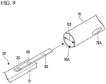
- the attachment holes 25 are portions to which a jig such as wire is attached when the imaging module 1 is attached to a catheter. In a state where the jig is attached to the attachment holes 25, by inserting the jig into a tube forming the catheter and drawing the jig into the tube, it is possible to dispose the second substrate 20 inside the tube. The details will be described with reference to FIG. 9 .
- Identification Number used for individual identification of the imaging module 1 may be represented at the portion adjacent to the position at which the attachment holes 25 are formed.
- the second substrate 20 includes an external connection terminal 24 formed on the second substrate main body 21, and the external connection terminal 24 is electrically connected to the second wiring 22.
- the external connection terminal 24 is connected to an external device. Note that, the external connection terminal 24 and the second wiring 22 are simultaneously formed on the second substrate main body 21.
- the embodiment shows the configuration in which the center conductor terminal 221 and the external conductor terminal 22J are formed on the upper face 21U serving as one of the surfaces of the second substrate main body 21; however, the invention is not limited to this configuration.
- the center conductor terminal 221 and the external conductor terminal 22J may be formed on the lower face 21L serving as the other surface of the second substrate main body 21.
- a wiring structure is adopted in which a center conductor terminal and an external conductor terminal formed on the lower face 21L are connected to the center conductor 31 and the external conductor 33, respectively.
- the invention is not limited to a structure in which the center conductor terminal 221 and the external conductor terminal 22J are formed only on one of the surfaces of the second substrate main body 21.
- a structure may be adopted in which conductor terminals are formed on both surfaces of the second substrate main body 21, that is, on the upper face 21U and the lower face 21L, and the center conductor 31 and the external conductor 33 are connected to the conductor terminals.
- a wiring structure may be adopted in which the through electrode 28 is not formed depending on a wiring pattern.
- a configuration in which conductor terminals are formed on both surfaces of the second substrate main body 21 for example, a configuration is adopted in which, a center conductor terminal and an external conductor terminal to which a center conductor 31A and an external conductor 33A of a first coaxial cable 30A (which will be described later) are connected, respectively, are formed on the upper face 21U, and a center conductor terminal and an external conductor terminal to which a center conductor 31B and an external conductor 33B of a second coaxial cable 30B (which will be described later) are connected, respectively, are formed on the lower face 21L.
- a structure may be adopted in which a center conductor terminal is provided on one of the upper face 21U and the lower face 21L and an external conductor terminal is provided on the other face.
- the solid-state image sensing device 40 includes a light-receiving face 41, an electrode surface 43 located on the opposite side of the light-receiving face 41, and the image-sensing device electrodes 42U and 42L (two image-sensing device electrodes) provided on the electrode surface 43.
- the first substrate 10 is connected to the electrode surface 43 so that the outer end face 11E of the first substrate main body 11 is located between the image-sensing device electrodes 42U and 42L.
- the image-sensing device electrode 42U has a surface parallel to the direction substantially orthogonal to the electrode terminal 12HU
- the image-sensing device electrode 42L has a surface parallel to the direction substantially orthogonal to the electrode terminal 12HL.
- the solder 15 connects the image-sensing device electrode 42U and the electrode terminal 12HU which are substantially orthogonal to each other, and connects the image-sensing device electrode 42L and the electrode terminal 12HL which are substantially orthogonal to each other.
- FIG. 1 shows the image-sensing device electrodes 42U and 42L which are arranged at the upper position and the lower position, respectively; however, when seen in a plan view of the electrode surface 43 (in a plan view showing the electrode surface 43 when viewed in a vertical direction) four image-sensing device electrodes 42 are arranged on the electrode surface 43. That is, two image-sensing device electrodes 42U and two image-sensing device electrodes 42L are formed on the electrode surface 43.
- the lens housing 50 is connected to the light-receiving face 41, and a lens unit such as an object lens is mounted on the lens housing 50.
- a lens unit such as an object lens
- the solid-state image sensing device 40 for example, a CMOS (complementary metal oxide semiconductor) is preferably used.
- FIG. 2 is a cross-sectional view showing the signal cable 30 of the imaging module according to the first embodiment of the invention.
- the signal cable 30 is provided between the first substrate 10 and the second substrate 20 and includes two coaxial cable (signal line, a first coaxial cable 30A, a second coaxial cable 30B), a shield conductor 30C that surrounds the first coaxial cable 30A and the second coaxial cable 30B, and an outer coating 30D that surrounds the shield conductor 30C.
- the shield conductor 30C is provided on the entire inner peripheral surface of the outer coating 30D and is formed in a layer shape.
- the structure is shown in which the shield conductor 30C is disposed separately from a cable contact portion at which the side portions of the first coaxial cable 30A and the second coaxial cable 30B are in contact with each other, and a space 30E is present between the cable contact portion and the shield conductor 30C located at both sides of the cable contact portion.
- a cross-sectional structure of the signal cable 30 a cross-sectional structure is applicable, in which the shield conductor 30C enters a region of the space 30E shown in FIG. 2 and a space is substantially absent among the first coaxial cable 30A, the second coaxial cable 30B, and the layer-shaped shield conductor 30C.
- Each of the coaxial cables 30A and 30B includes a center conductor 31 (31A, 31B), an internal insulator 32 (32A, 32B), an external conductor 33 (33A, 33B), and an external insulator 34 (34A, 34B).
- the center conductor 31 is used as a signal line that supplies a signal to the solid-state image sensing device 40
- the external conductor 33 is used as a power supply line that supplies electric power to the solid-state image sensing device 40.
- the center conductor 31 (31A, 31B) electrically connects the center conductor terminal 121 of the first substrate 10 to the center conductor terminal 221 of the second substrate 20.
- the external conductor 33 (33A, 33B) electrically connects the external conductor terminal 12J of the first substrate 10 to the external conductor terminal 22J of the second substrate 20.
- the shield conductor 30C and the outer coating 30D surrounds the first coaxial cable 30A and the second coaxial cable 30B over the entire signal cable 30.
- the shield conductor 30C and the outer coating 30D are removed at the position close to the first substrate 10 (the position close to the inner end face 11F shown in FIG. 1 ), and the first coaxial cable 30A and the second coaxial cable 30B are exposed.
- the outer coating 30D is removed at the position close to the second substrate 20 (the position close to the inner end face 21F shown in FIG. 1 ), and the shield conductor 30C is exposed, and the shield conductor 30C is electrically connected to the shield terminal 22K via the solder 29.
- the shield terminal is connected to, for example, GND, and therefore the shield conductor 30C is grounded.
- the external conductor 33 and the center conductor 31 which constitute each of the first coaxial cable 30A and the second coaxial cable 30B are exposed so as to correspond to wiring patterns of the first substrate 10 and the second substrate 20.
- the external conductor 33 (33A, 33B) is exposed from the external insulator 34 (34A, 34B).
- the exposed external conductor 33 (33A, 33B) is electrically connected to the external conductor terminal 22J via the solder 27.
- the center conductor 31 (31A, 31B) is exposed from the internal insulator 32 (32A, 32B).
- the exposed center conductor 31 (31A, 31B) is electrically connected to the center conductor terminal 221 via the solder 26.
- FIG. 3 is a view showing a schematic configuration of the imaging module according to the first embodiment of the invention and is an explanatory view showing a positional relationship among the first substrate 10, the second substrate 20, and the signal cable 30.
- the surface 10A (upper face 11U) on which the first cable terminal is connected to the signal cable 30 and the surface 20A (upper face 21U) on which the second cable terminal is connected to the signal cable 30 are located on the same plane. Furthermore, the first substrate 10 is connected to the second substrate 20 with the signal cable 30 interposed therebetween so that one signal cable 30 corresponds to a pair of the first substrate 10 and the second substrate 20.
- the surface 10A on which the center conductor terminal 121 and the external conductor terminal 12J of the first substrate 10 are formed is referred to as an upper face
- a surface opposite to the surface 10A is referred to as a lower face
- the surface 20A on which the center conductor terminal 221 and the external conductor terminal 22J of the second substrate 20 are formed is referred to as an upper face
- a surface opposite to the surface 20A is referred to as a lower face.
- the first substrate 10 and the second substrate 20 in a state where the lower face of each of the first substrate 10 and the second substrate 20 are in contact with the same horizontal plane, the first substrate 10 and the second substrate 20 can be mounted on the same horizontal plane.
- the signal cable 30 is located at the upper side of the first substrate 10 and the second substrate 20.
- the signal cable 30 can be connected to each of the surfaces 10A and 20A by soldering, and it is possible to simplify a step of manufacturing the imaging module 1.
- the imaging module 1 regarding a plurality of pairs of the first substrate 10 and the second substrate 20 and a plurality of signal cables 30, it is necessary to collectively connect the pairs of the first substrate 10 and the second substrate 20 to the plurality of the signal cables 30 by soldering so that one signal cable 30 corresponds to each pair of the first substrate 10 and the second substrate 20.
- connection step since the surface 10A of the first substrate 10 and the surface 20A of the second substrate 20 are arranged on the same plane, it is possible to supply solder to the surfaces 10A and 20A so as to be directed in the Z-direction (direction of gravitational force), and it is thereby possible to increase the manufacturing efficiency in the mass production line of the imaging module 1.
- FIG. 4 is a perspective view showing a light-receiving face of the solid-state image sensing device of the imaging module according to the first embodiment of the invention.
- FIG. 5A is a perspective view showing an end of the second substrate of the imaging module according to the first embodiment of the invention.
- FIG. 5B is a side view showing an end of the second substrate of the imaging module according to the first embodiment of the invention.
- the wiring structure of the first substrate 10 shown in FIG. 1 i.e., the first wiring 12 formed on the first substrate main body 11, the solder 15 to 17, the signal cable 30 connected to the first substrate 10, and the lens housing 50
- the wiring structure the second substrate 20 shown in FIG. 1 i.e., the second wiring 22 formed on the second substrate main body 21, the solder 26, 27, the signal cable 30 connected to the second substrate 20
- the second substrate 20 and the signal cable 30 connected to a surface of the second substrate 20 are shown in FIG. 5B .
- a length of a first diagonal line T1 on the light-receiving face 41 of the solid-state image sensing device 40 is defined as D1 and a length of a second diagonal line T2 on the outer end face 21E of the second substrate main body 21 is defined as D2, the length D2 is less than or equal to the length D1 (condition D1 ⁇ D2 is satisfied).
- the length of the first diagonal line T1 means the distance between two corners that are located at the positions opposite to each other on the light-receiving face 41.
- the length of the second diagonal line T2 means the distance between two corners that are opposite to each other on the outer end face 21E.
- the signal cable 30 is arranged inside the circumscribed circle C of the second substrate main body 21.
- the diameter of the circumscribed circle C corresponds to the length D2 of the second diagonal line T2.
- FIGS. 6A and 6B are views each showing a wiring pattern formed on the second substrate of the imaging module according to the first embodiment of the invention.
- FIG. 6A shows a wiring pattern of the upper face wiring 22U formed on the upper face 21U of the second substrate main body 21.
- FIG. 6B shows a wiring pattern of the lower face wiring 22L formed on the lower face 21L of the second substrate main body 21. Note that, FIG. 6B is not a bottom view showing the lower face 21L but is a projection view as seen from the upper face 21U shown in FIG. 6A .
- the resists 23A and 23B are formed on the upper face 21U of the second substrate main body 21 shown in FIG. 1 ; however, the resists 23A and 23B are omitted in FIGS. 6A and 6B .
- reference numeral 22JA corresponds to the external conductor terminal 22J and is a terminal connected to the external conductor 33A of the first coaxial cable 30A via the solder 27.
- reference numeral 22JB corresponds to the external conductor terminal 22J and is a terminal connected to the external conductor 33B of the second coaxial cable 30B via the solder 27.
- it will be referred to as an external conductor terminal 22JB.
- Reference numeral 22IA corresponds to the center conductor terminal 221 and is a terminal connected to the center conductor 31A of the first coaxial cable 30A via the solder 26.
- a center conductor terminal 22IA corresponds to the center conductor terminal 22IA.
- Reference numeral 22IB corresponds to the center conductor terminal 221 and is a terminal connected to the center conductor 31B of the second coaxial cable 30B via the solder 26.
- it will be referred to as a center conductor terminal 22IB.
- Reference numeral 22K represents a terminal that is provided at the position adjacent to the inner end face 21F of the second substrate main body 21 and is connected to the shield conductor 30C.
- a shield terminal 22K represents a terminal that is provided at the position adjacent to the inner end face 21F of the second substrate main body 21 and is connected to the shield conductor 30C.
- Reference numerals 24K, 24IB, 24IA, 24JA, and 24JB represent external connection terminals formed on the upper face 21U and correspond to the external connection terminal 24 shown in FIG. 1 .
- the external connection terminals 24K, 24IB, 24IA, 24JA, and 24JB align in the extending direction of the second substrate main body 21.
- Reference numeral 22L represents a drawing wiring that connects the center conductor terminal 22IA to the external connection terminal 24IA.
- Reference numeral 22M represents a drawing wiring that connects the external conductor terminal 22JB to the external connection terminal 24JB.
- Reference numeral 22N represents a drawing wiring that connects the center conductor terminal 22IB to the external connection terminal 24IB.
- the drawing wiring 22N is a wiring having a linear part that extends straight in the extending direction of the second substrate main body 21.
- the drawing wiring 22M is a wiring having a linear part that extends straight in the extending direction of the second substrate main body 21 and a bending part that bends so as to follow the shape of the external connection terminal 24IB.
- the drawing wiring 22L is a wring having a wiring part that extends straight in the extending direction of the second substrate main body 21 and a bending part that bends so as to follow the shape of the drawing wiring 22M.
- Reference numerals 28A, 28B, 28C, and 28D are each a through electrode correspond to the through electrode 28 shown in FIG. 1 .
- Through electrode 28A is connected to the shield terminal 22K
- the through electrode 28B is connected to the external conductor terminal 22JA
- the through electrode 28C is connected to the external connection terminal 24JA
- the through electrode 28D is connected to the external connection terminal 24K.
- the lower face wiring 22L formed on the lower face 21L has drawing wirings 22O and 22P.
- the drawing wiring 22O connects the through electrode 28B to the through electrode 28C.
- the drawing wiring 22P connects the through electrode 28A to the through electrode 28D.
- the external conductor terminals, the center conductor terminals, the external connection terminals, and the drawing wirings which are described above can be collectively formed by patterning using a known photolithographic technique or the like. Furthermore, the through electrodes 28A, 28B, 28C, and 28D can also be formed by a known method.
- the external conductor terminals and the center conductor terminals of the coaxial cable 30 can be connected to the external connection terminals 24K, 24IB, 24IA, 24JA, and 24JB, and it is possible to easily connect the terminals to the external device.
- the wiring pattern formed on the second substrate 20 is not limited to the structure shown in FIGS. 6A and 6B .
- a wiring structure shown in FIGS. 7A and 7B can be adopted.
- FIGS. 7A and 7B are views each showing a wiring pattern formed on the second substrate of the imaging module according to a modified example of the first embodiment of the invention.
- FIG. 7A shows a wiring pattern of the upper face wiring 22U formed on the upper face 21U of the second substrate main body 21.
- FIG. 7B shows a wiring pattern of the lower face wiring 22L formed on the lower face 21L of the second substrate main body 21. Note that, FIG. 7B is not a bottom view showing the lower face 21L but is a projection view as seen from the upper face 21U shown in FIG. 7A .
- the resists 23A and 23B are formed on the upper face 21U of the second substrate main body 21 shown in FIG. 1 ; however, the resists 23A and 23B are omitted in FIGS. 7A and 7B .
- identical reference numerals are used for the elements that are identical to those of FIGS. 6A and 6B , and the explanations thereof are omitted or simplified here.
- the shield terminal 22K is connected to the through electrode 28A
- the external conductor terminal 22JB is connected to the through electrode 28B
- the external conductor terminal 22JA is connected to the through electrode 28C
- the center conductor terminal 22IA is connected to the through electrode 28D
- the center conductor terminal 22IB is connected to the through electrode 28E.
- the external connection terminals 24K, 24JB, 24JA, 24IA, and 24IB align in the extending direction of the second substrate main body 21.
- the external connection terminal 24K is connected to the shield terminal 22K through the through electrode 28A.
- the external connection terminal 24JB is connected to the external conductor terminal 22JB through the through electrode 28B.
- the external connection terminal 24JA is connected to the external conductor terminal 22JA through the through electrode 28C.
- the external connection terminal 24IA is connected to the center conductor terminal 22IA through the through electrode 28D.
- the external connection terminal 24IB is connected to the center conductor terminal 22IB through the through electrode 28E.
- the external conductor terminals and the center conductor terminals of the coaxial cable 30 can be connected to the external connection terminals 24K, 24JB, 24JA, 24IA, and 24IB, and it is possible to easily connect the terminals to the external device.
- the condition D condition D1 ⁇ D2 is satisfied, furthermore, the signal cable 30 is disposed inside the circumscribed circle C of the second substrate main body 21, and the circumscribed circle C has a diameter corresponding to the length of the second diagonal line T2. Because of this, the second substrate 20 can be smaller than the solid-state image sensing device 40. Also, when the imaging module 1 is attached to a medical instrument such as a catheter, firstly, the second substrate 20 is inserted into a hole to which the solid-state image sensing device 40 is to be attached, and the imaging module 1 can be easily drawn into the medical instrument.
- D2 is larger than D1
- it is necessary to push the imaging module into the medical instrument from the rear thereof or a size of a hole to which a solid-state image sensing device is to be attached is necessary to be larger than D2.
- the imaging module is pushed into the inside of the medical instrument by utilizing the rigidity of a signal cable.
- the signal cable is elastic, it is not possible to effectively push the imaging module into the inside of the medical instrument, and workability therefor becomes deteriorated.
- FIG. 8 is a partial cross-sectional view showing a schematic configuration of a catheter 60 according to the second embodiment of the invention.
- the catheter 60 shown in FIG. 8 is an imaging-module-attached catheter including the above-mentioned imaging module 1.
- the position at which the solid-state image sensing device 40 or the first substrate 10 is disposed may be referred to as a front side, and the position at which the second substrate 20 is disposed may be referred to as a rear side.
- the catheter 60 includes a tube 70 that is made of, for example, silicon or the like and has an insulation property.
- silicon is adopted as a material used to form the tube 70, a flexible material or a metal material other than silicon may be used.
- a flexible material silicon, polyurethane, polyethylene, polytetrafluoroethylene (PTFE, for example, Teflon (registered trademark)), or the like is adopted.
- PTFE polytetrafluoroethylene
- a metal material titanium, a titanium alloy, a stainless steel, or the like is adopted.
- ceramic material may be used as a material used to form the tube 70.
- the tube 70 includes a module insertion opening 70A, a cable insertion opening 70B, a module arrangement region 71 in which the first substrate 10 and part of the signal cable 30 which form the imaging module 1 are disposed, a channel 72, a cable arrangement region 75, and a second substrate output port 76.
- the module insertion opening 70A is an opening through which the imaging module 1 is inserted into the tube 70
- the cable insertion opening 70B is an opening into which the second substrate 20 and the signal cable 30 which form the imaging module 1 are inserted
- the cable arrangement region 75 is a tube through which the second substrate 20 passes
- the second substrate output port 76 is an opening through which the second substrate 20 is extracted from the tube 70.
- the solid-state image sensing device 40 is attached to the module insertion opening 70A, the first substrate 10 and part of the signal cable 30 are disposed in the module arrangement region 71, the signal cable 30 is disposed in the cable arrangement region 75, and the second substrate 20 is disposed outside the second substrate output port 76.
- the tube 70 has a front opening 72A located close to the first substrate 10 and a rear opening 72B located close to the second substrate 20, and the pathway formed between the front opening 72A and the rear opening 72B is the channel 72.
- the channel 72 is located between the external conductor terminal 12J (first cable terminal) and the external conductor terminal 22J (second cable terminal) and is disposed adjacent to the cable arrangement region 75.
- the channel 72 is isolated from the cable arrangement region 75 by an inner wall 74.
- the channel 72 is disposed within an outline of the solid-state image sensing device 40 on a plane of projection as seen in a direction from the solid-state image sensing device 40 to the inner end face 11F.
- an internal diameter D3 of the module insertion opening 70A is set less than or equal to the length D1 and larger than or equal to the length D2 (condition D1 ⁇ D3 ⁇ D2 is satisfied).
- an internal diameter D4 of the cable insertion opening 70B (cable arrangement region 75) is set less than or equal to the length D3 and larger than or equal to the length D2 (condition D3 ⁇ D4 ⁇ D2).
- the channel 72 may be used as a lumen and may be used as a working channel.
- a solvent medium injection lumen that ejects a solvent medium toward the front of the catheter 60 or a vacuuming lumen that removes liquid present in front of the catheter 60 can be provided in the tube 70.
- a treatment tool indicated by reference numeral 73 may be inserted into the channel 72.
- the treatment tool 73 for example, various forcipes, a snare, a guide wire, a stent, a laser treatment tool, a high-frequency treatment tool, or the like is adopted.
- the imaging module 1 having the first substrate 10 and the second substrate 20 which are connected to each other with the signal cable 30 interposed therebetween is prepared.
- a jig 80 is prepared, the jig 80 is attached to the attachment holes 25 of the second substrate main body 21.
- the jig 80 has a length such that the jig slightly extends from the end of the second substrate main body 21; however, the length of the jig 80 is not particularly limited.
- a material used to form the jig 80 a material is adopted which has a higher degree of rigidity than that of a material the tube 70 and does not bend in the operation of drawing into the imaging module 1 into the inside of the tube 70.
- the jig 80 is inserted into the module insertion opening 70A, furthermore, the jig 80 is inserted through the cable insertion opening 70B into the inside of the cable arrangement region 75, and the jig 80 moves toward the second substrate output port 76. Finally, the jig 80 is extracted from the second substrate output port 76.
- the second substrate 20 is inserted into the module insertion opening 70A, the second substrate 20 is inserted through the cable insertion opening 70B into the inside of the cable arrangement region 75, the second substrate 20 moves toward the second substrate output port 76. Finally, the second substrate 20 is extracted from the second substrate output port 76.
- the signal cable 30 connected to the second substrate 20 is disposed inside the cable arrangement region 75. Furthermore, the first substrate 10 and part of the signal cable 30 are disposed in the module arrangement region 71.
- the solid-state image sensing device 40 comes into contact with the module insertion opening 70A.
- the internal diameter D3 of the module insertion opening 70A is less than or equal to the length D1 of the first diagonal line T1 on the light-receiving face 41 (condition D1 ⁇ D3), the solid-state image sensing device 40 is in a state of being attached to the module insertion opening 70A without being inserted into the inside of the tube 70.
- the imaging module 1 it is possible to easily draw the imaging module 1 into the inside of the tube 70 of the catheter 60.
- the second substrate 20 can be smoothly extracted from the second substrate output port 76 without being caught by the module insertion opening 70A and the cable insertion opening 70B.
- an outer diameter of the catheter 60 does not increase, it is possible to achieve the catheter 60 that includes both the channel and the imaging module and has a small diameter.
- a wire or the like may be used as the jig 80 in the above-described second embodiment.
- a wire is prepared which has a length longer than the overall length of the tube 70, the wire is inserted into the inside of the cable arrangement region 75 so that the wire is exposed from the module insertion opening 70A and the second substrate output port 76. Thereafter, the end of the wire is attached to the attachment holes 25 shown in FIG. 9 , and the wire exposed from the second substrate output port 76 is pulled to the outside. Accordingly, a tension occurs in the wire, the second substrate 20 is inserted into the module insertion opening 70A. Even in the case of using the above-described wire as the jig 80, the same effects as the in the aforementioned case is obtained.
- 1...imaging module 10...first substrate, 11...first substrate main body, 11E, 21E...outer end face (end face), 11F, 21F...inner end face, 11L, 21L... lower face, 11U, 21U...upper face, 12...first wiring, 12HL, 12HU...electrode terminal, 12I, 22I, 22IA, 22IB...center conductor terminal, 12J, 22J, 22JA, 22JB...external conductor terminal, 12L, 22L...lower face wiring, 12U, 22U...upper face wiring, 13A, 13B...upper face resist (resist), 13C...lower face resist (resist), 14, 28, 28A, 28B, 28C, and 28D, 28E...through electrode, 15, 16, 17, 26, 27, 29...solder, 20...second substrate, 21...second substrate main body, 22...second wiring, 22K...shield terminal, 22L, 22M, 22N, 22O, 22P...drawing wiring, 23, 23A, 23B...resist, 24, 24IA,
Landscapes
- Health & Medical Sciences (AREA)
- Life Sciences & Earth Sciences (AREA)
- Physics & Mathematics (AREA)
- Surgery (AREA)
- Optics & Photonics (AREA)
- Engineering & Computer Science (AREA)
- Animal Behavior & Ethology (AREA)
- Heart & Thoracic Surgery (AREA)
- Veterinary Medicine (AREA)
- Biophysics (AREA)
- Nuclear Medicine, Radiotherapy & Molecular Imaging (AREA)
- Pathology (AREA)
- Radiology & Medical Imaging (AREA)
- Public Health (AREA)
- Biomedical Technology (AREA)
- General Health & Medical Sciences (AREA)
- Medical Informatics (AREA)
- Molecular Biology (AREA)
- Astronomy & Astrophysics (AREA)
- General Physics & Mathematics (AREA)
- Signal Processing (AREA)
- Multimedia (AREA)
- Endoscopes (AREA)
- Studio Devices (AREA)
- Instruments For Viewing The Inside Of Hollow Bodies (AREA)
Abstract
Description
- The present invention relates to an imaging module and an imaging-module-attached catheter.
- This application claims priority from Japanese Patent Application No.
2017-167993 filed on August 31, 2017 - An imaging module having a configuration in which a solid-state image sensing device (hereinbelow, may be simply referred to as an image-sensing device) is electrically connected to an end of an electrical cable with a wiring substrate interposed therebetween is often employed in electronic endoscopes (for example, Patent Document 1).
- In this kind of imaging module, a plurality of ends of the electrical cable are electrically connected to wiring of the wiring substrate, and each electrical cable is electrically connected to the image-sensing device via the wiring of the wiring substrate.
- (Patent Document 1) Japanese Unexamined Patent Application, First Publication No.
2006-109097 - In an imaging device such as an endoscope using the aforementioned imaging module, a configuration is often employed in which a plurality of electrical cables connected to an imaging module and a wiring substrate of the imaging module are accommodated in a tube. Furthermore, an back end that is opposite to the imaging module side of the electrical cable of this imaging device is drawn from the tube and is electrically connected to an image information processing device that receives imaging signals from the electrical cable and displays an image on a display device such as a monitor.
- In recent years, it has been studied that an imaging module is applied to a medical instrument such as a catheter that is provided with a lumen or a working channel. For example, in the case of inserting an imaging module into a medical tube having a hole into which an image-sensing device is to be incorporated, it is necessary to draw the imaging module into the tube through the hole. However, in the case where a substrate size of the imaging module is larger, there is a problem in that it is difficult to smoothly insert the imaging module into the hole formed in the tube.
- One aspect of the invention provides an imaging module that can be easily drawn into a medical instrument that is provided with a channel such as lumen and has a small diameter.
- In order to solve the above problem, an imaging module according to a first aspect of the invention includes: an image-sensing device including an image-sensing device electrode; a first substrate including a first substrate main body serving as an insulating member, a first wiring formed on the first substrate main body, an electrode terminal electrically connected to the image-sensing device electrode and the first wiring, and a first cable terminal that is formed on a surface of the first substrate main body and is electrically connected to the first wiring; one second substrate including a second substrate main body serving as an insulating member, a second wiring formed on the second substrate main body, and a second cable terminal that is formed on a surface of the second substrate main body and is electrically connected to the second wiring; and a signal cable that is provided between the first substrate and the second substrate and electrically connects the first cable terminal to the second cable terminal, wherein where a length of a first diagonal line on a light-receiving face of the image-sensing device is defined as D1 and a length of a second diagonal line on an end face of the second substrate main body is defined as D2, the length D2 is less than or equal to the length D1.
- In the imaging module according to the first aspect of the invention, the signal cable may be arranged inside a circumscribed circle of the second substrate main body, and the circumscribed circle having a diameter corresponding to the length of the second diagonal line.
- In the imaging module according to the first aspect of the invention, the image-sensing device may have an electrode surface on which the image-sensing device electrode is provided, and the first substrate may be connected to the electrode surface so that an end face of the first substrate main body is located between two image-sensing device electrodes.
- In the imaging module according to the first aspect of the invention, the second substrate may have a first surface, a second surface opposite to the first surface, and a through electrode that penetrates through the second substrate main body between the first surface and the second surface, and the second wiring may be formed on the first surface and on the second surface and may be electrically connected to the through electrode.
- In the imaging module according to the first aspect of the invention, the second substrate may include an external connection terminal formed on the second substrate main body, and the external connection terminal may be electrically connected to the second wiring.
- In the imaging module according to the first aspect of the invention, the external connection terminal may be formed on the first surface of the second substrate.
- In the imaging module according to the first aspect of the invention, the external connection terminal may be formed on the second surface of the second substrate.
- In the imaging module according to the first aspect of the invention, the signal cable may be a coaxial cable.
- An imaging-module-attached catheter according to a second aspect of the invention includes: the imaging module according to the aforementioned first aspect; and a tube including: a module arrangement region in which the first substrate and part of the signal cable are arranged; and a channel that is located between the first cable terminal and the second cable terminal and is next to the module arrangement region, wherein as seen from the image-sensing device, the channel is disposed within an outline of the image-sensing device on a plane of projection.
- As described above, according to the above-mentioned aspect of the invention, it is possible to provide an imaging module that can be easily drawn into a medical instrument that is provided with a channel such as lumen and has a small diameter. Additionally, it is possible to provide a catheter including both a channel and an imaging module and having small-diameter.
-
-
FIG. 1 is a partial cross-sectional view showing a schematic configuration of an imaging module according to a first embodiment of the invention. -
FIG. 2 is a cross-sectional view showing a signal cable of the imaging module according to the first embodiment of the invention. -
FIG. 3 is a view showing a schematic configuration of the imaging module according to the first embodiment of the invention and is an explanatory view showing a positional relationship among a first substrate, a second substrate, and a signal cable. -
FIG. 4 is a perspective view showing a light-receiving face of a solid-state image sensing device of the imaging module according to the first embodiment of the invention. -
FIG. 5A is a perspective view showing an end of a second substrate of the imaging module according to the first embodiment of the invention. -
FIG. 5B is a side view showing an end of a second substrate of the imaging module according to the first embodiment of the invention. -
FIG. 6A is a plan view showing a wiring pattern formed on the second substrate of the imaging module according to the first embodiment of the invention and is an explanatory view showing a connection structure between the image-sensing device and the signal cable. -
FIG. 6B is a plan view showing a wiring pattern formed on the second substrate of the imaging module according to the first embodiment of the invention and is an explanatory view showing a connection structure between the image-sensing device and the signal cable. -
FIG. 7A is a plan view showing a wiring pattern formed on the second substrate of an imaging module according to a modified example of the first embodiment of the invention and is an explanatory view showing a connection structure between the image-sensing device and the signal cable. -
FIG. 7B is a plan view showing a wiring pattern formed on the second substrate of an imaging module according to a modified example of the first embodiment of the invention and is an explanatory view showing a connection structure between the image-sensing device and the signal cable. -
FIG. 8 is a partial cross-sectional view showing a schematic configuration of an imaging-module-attached catheter according to a second embodiment of the invention. -
FIG. 9 is an explanatory diagram showing operation of drawing an imaging module into a tube forming the imaging-module-attached catheter according to the second embodiment of the invention. - Hereinafter, an embodiment of the invention will be described with reference to drawings.
- In the drawings showing embodiments of the invention, in order for the respective components to be of understandable size in the drawings, the dimensions and the proportions of the components are modified as needed compared with the real components.
-
FIG. 1 is a partial cross-sectional view showing a schematic configuration of theimaging module 1 according to the first embodiment of the invention. - The
imaging module 1 includes afirst substrate 10, asecond substrate 20, asignal cable 30, a solid-state image sensing device 40 (image-sensing device), and alens housing 50. - The
first substrate 10 includes a first substratemain body 11 serving as an insulating member and a first wiring 12 (upper face wiring 12U, andlower face wiring 12L) formed on the first substratemain body 11. The first substratemain body 11 has anupper face 11U (first surface) and alower face 11L (second surface) opposite to theupper face 11U. Theupper face wiring 12U is formed on theupper face 11U. Thelower face wiring 12L is formed on thelower face 11L. Thefirst wiring 12 has a conductive wiring pattern formed on both theupper face 11U and thelower face 11L. - The first substrate main body 11 (first substrate 10) has an
outer end face 11E (end face) connected to the solid-stateimage sensing device 40 and aninner end face 11F opposite to theouter end face 11E. In a state where theouter end face 11E is connected to the solid-stateimage sensing device 40, the first substratemain body 11 extends in a direction substantially orthogonal to an electrode surface 43 of the solid-stateimage sensing device 40. Theinner end face 11F is exposed to a space adjacent to thesignal cable 30. - The
first substrate 10 includes a throughelectrode 14 that penetrates through the first substratemain body 11 between theupper face 11U and thelower face 11L. The throughelectrode 14 electrically connects theupper face wiring 12U to thelower face wiring 12L. - An electrode terminal 12HU that is electrically connected to the
upper face wiring 12U is formed on theupper face 11U. An electrode terminal 12HL that is electrically connected to thelower face wiring 12L is formed on thelower face 11L. That is, electrode terminals are formed on both theupper face 11U and thelower face 11L. The electrode terminal 12HU is electrically connected viasolder 15 to an image-sensingdevice electrode 42U (42) of the solid-stateimage sensing device 40 which will be described later. The electrode terminal 12HL is electrically connected to an image-sensing device electrode 42L (42) of the solid-stateimage sensing device 40 via thesolder 15. - A center conductor terminal 121 (first cable terminal) and an
external conductor terminal 12J (first cable terminal) are formed on one surface of the first substratemain body 11, that is, on theupper face 11U. Thecenter conductor terminal 121 and theexternal conductor terminal 12 are electrically connected to theupper face wiring 12U. Thecenter conductor terminal 121 is electrically connected viasolder 16 to acenter conductor 31 of thesignal cable 30 which will be described later. Theexternal conductor terminal 12J is electrically connected viasolder 17 to anexternal conductor 33 of thesignal cable 30. - Upper face resists 13A and 13B (13) are formed on the
upper face 11U of the first substratemain body 11 so as to coat a surface of theupper face wiring 12U. The upper face resist 13A is formed between thesolder 15 and thesolder 16. The upper face resist 13B is formed between thesolder 16 and thesolder 17. A lower face resist 13C (13) is formed on thelower face 11L of the first substratemain body 11 so as to coat a surface of thelower face wiring 12L. - In
FIG. 1 , as seen in the direction from the solid-stateimage sensing device 40 toward the inner end face 11F, thesignal cable 30 is disposed within an outline of the solid-stateimage sensing device 40 on a plane of projection, and thesignal cable 30 does not partially protrude from the outline of the solid-stateimage sensing device 40 shown in the plane of projection of the solid-stateimage sensing device 40. - Note that, a resin mold may be formed on the
upper face 11U of the first substratemain body 11 so as to coat thesolder center conductor 31 and theexternal conductor 33 of thesignal cable 30, and the upper face resists 13A and 13B. By forming the resin mold on theupper face 11U as stated above, it is possible to increase the strength of the first substratemain body 11. - Moreover, a resin mold may be formed on the
lower face 11L of the first substratemain body 11 so as to coat thesolder 15 and the lower face resist 13C. By forming the resin mold on thelower face 11L as stated above, it is possible to increase the strength of the first substratemain body 11. - Furthermore, a resin mold may be formed on both surfaces of the first substrate
main body 11. In this case, it is possible to further increase the strength of the first substratemain body 11 by the resin mold formed on both surfaces. - Particularly, as an example, the embodiment shows the configuration in which the
center conductor terminal 121 and theexternal conductor terminal 12J are formed on theupper face 11U serving as one of the surfaces of the first substratemain body 11; however, the invention is not limited to this configuration. Thecenter conductor terminal 121 and theexternal conductor terminal 12J may be formed on thelower face 11L serving as the other surface of the first substratemain body 11. In this case, a wiring structure is adopted in which a center conductor terminal and an external conductor terminal formed on thelower face 11L are connected to thecenter conductor 31 and theexternal conductor 33, respectively. - Furthermore, the invention is not limited to a structure in which the
center conductor terminal 121 and theexternal conductor terminal 12J are formed only on one of the surfaces of the first substratemain body 11. A structure may be adopted in which conductor terminals are formed on both surfaces of the first substratemain body 11, that is, on theupper face 11U and thelower face 11L, and thecenter conductor 31 and theexternal conductor 33 are connected to the conductor terminals. In addition, in the structure in which the conductor terminals are formed on both surfaces of the first substratemain body 11, a wiring structure may be adopted in which the throughelectrode 14 is not formed depending on a wiring pattern. - As a configuration in which conductor terminals are formed on both surfaces of the first substrate
main body 11, for example, a configuration is adopted in which, a center conductor terminal and an external conductor terminal to which acenter conductor 31A and anexternal conductor 33A of a firstcoaxial cable 30A (which will be described later) are connected, respectively, are formed on theupper face 11U, and a center conductor terminal and an external conductor terminal to which acenter conductor 31B and anexternal conductor 33B of a secondcoaxial cable 30B (which will be described later) are connected, respectively, are formed on thelower face 11L. - Additionally, a structure may be adopted in which a center conductor terminal is provided on one of the
upper face 11U and thelower face 11L and an external conductor terminal is provided on the other face. - The
second substrate 20 includes a second substratemain body 21 serving as an insulating member and asecond wiring 22 formed on the second substratemain body 21. The second substratemain body 21 has anupper face 21U (first surface) and alower face 21L (second surface) opposite to theupper face 21U. Anupper face wiring 22U forming thesecond wiring 22 is formed on theupper face 21U. Alower face wiring 22L forming thesecond wiring 22 is formed on thelower face 21L. Thesecond wiring 22 includes a conductive wiring pattern formed on both theupper face 21U and thelower face 21L. The wiring pattern will be described later. Particularly, in the embodiment, the number ofsecond substrates 20 is not two or more but is one. - Furthermore, the
second substrate 20 includes a throughelectrode 28 that penetrates through the second substratemain body 21 between theupper face 21U and thelower face 21L. The throughelectrode 28 electrically connects theupper face wiring 22U to thelower face wiring 22L. A structure of the throughelectrode 28 will be described later. - Moreover, the
second substrate 20 includes a center conductor terminal 221 (second cable terminal), anexternal conductor terminal 22J (second cable terminal), and ashield terminal 22K (second cable terminal). Thecenter conductor terminal 221, theexternal conductor terminal 22J, and theshield terminal 22K are formed on one of the surfaces of thesecond substrate 20, that is, on theupper face 21U, and are electrically connected to thesecond wiring 22. - The
center conductor terminal 221 is electrically connected viasolder 26 to thecenter conductor 31 of thesignal cable 30. Theexternal conductor terminal 22J is electrically connected viasolder 27 to theexternal conductor 33 of thesignal cable 30. Theshield terminal 22K is electrically connected viasolder 29 to ashield conductor 30C of thesignal cable 30. - Resists 23A and 23B (23) are formed on the
upper face 21U of the second substratemain body 21 so as to coat a surface of thesecond wiring 22. The resist 23B is formed between thesolder 26 and thesolder 27. The resist 23A is formed close to thesolder 26 on thecenter conductor terminal 221. - The second substrate
main body 21 has an inner end face 21F, anouter end face 21E (end face), and two attachment holes 25 provided close to theouter end face 21E. The attachment holes 25 are portions to which a jig such as wire is attached when theimaging module 1 is attached to a catheter. In a state where the jig is attached to the attachment holes 25, by inserting the jig into a tube forming the catheter and drawing the jig into the tube, it is possible to dispose thesecond substrate 20 inside the tube. The details will be described with reference toFIG. 9 . - Additionally, on the
upper face 21U or thelower face 21L of the second substratemain body 21, Identification Number used for individual identification of theimaging module 1 may be represented at the portion adjacent to the position at which the attachment holes 25 are formed. - The
second substrate 20 includes anexternal connection terminal 24 formed on the second substratemain body 21, and theexternal connection terminal 24 is electrically connected to thesecond wiring 22. Theexternal connection terminal 24 is connected to an external device. Note that, theexternal connection terminal 24 and thesecond wiring 22 are simultaneously formed on the second substratemain body 21. - Particularly, as an example, the embodiment shows the configuration in which the
center conductor terminal 221 and theexternal conductor terminal 22J are formed on theupper face 21U serving as one of the surfaces of the second substratemain body 21; however, the invention is not limited to this configuration. Thecenter conductor terminal 221 and theexternal conductor terminal 22J may be formed on thelower face 21L serving as the other surface of the second substratemain body 21. In this case, a wiring structure is adopted in which a center conductor terminal and an external conductor terminal formed on thelower face 21L are connected to thecenter conductor 31 and theexternal conductor 33, respectively. - Furthermore, the invention is not limited to a structure in which the
center conductor terminal 221 and theexternal conductor terminal 22J are formed only on one of the surfaces of the second substratemain body 21. A structure may be adopted in which conductor terminals are formed on both surfaces of the second substratemain body 21, that is, on theupper face 21U and thelower face 21L, and thecenter conductor 31 and theexternal conductor 33 are connected to the conductor terminals. In addition, in the structure in which the conductor terminals are formed on both surfaces of the second substratemain body 21, a wiring structure may be adopted in which the throughelectrode 28 is not formed depending on a wiring pattern. - As a configuration in which conductor terminals are formed on both surfaces of the second substrate
main body 21, for example, a configuration is adopted in which, a center conductor terminal and an external conductor terminal to which acenter conductor 31A and anexternal conductor 33A of a firstcoaxial cable 30A (which will be described later) are connected, respectively, are formed on theupper face 21U, and a center conductor terminal and an external conductor terminal to which acenter conductor 31B and anexternal conductor 33B of a secondcoaxial cable 30B (which will be described later) are connected, respectively, are formed on thelower face 21L. - Additionally, a structure may be adopted in which a center conductor terminal is provided on one of the
upper face 21U and thelower face 21L and an external conductor terminal is provided on the other face. - The solid-state
image sensing device 40 includes a light-receivingface 41, an electrode surface 43 located on the opposite side of the light-receivingface 41, and the image-sensingdevice electrodes 42U and 42L (two image-sensing device electrodes) provided on the electrode surface 43. Thefirst substrate 10 is connected to the electrode surface 43 so that theouter end face 11E of the first substratemain body 11 is located between the image-sensingdevice electrodes 42U and 42L. - In a state where the
outer end face 11E of thefirst substrate 10 is connected to the electrode surface 43 of the solid-stateimage sensing device 40, the image-sensingdevice electrode 42U has a surface parallel to the direction substantially orthogonal to the electrode terminal 12HU, and the image-sensing device electrode 42L has a surface parallel to the direction substantially orthogonal to the electrode terminal 12HL. In this configuration, thesolder 15 connects the image-sensingdevice electrode 42U and the electrode terminal 12HU which are substantially orthogonal to each other, and connects the image-sensing device electrode 42L and the electrode terminal 12HL which are substantially orthogonal to each other. -
FIG. 1 shows the image-sensingdevice electrodes 42U and 42L which are arranged at the upper position and the lower position, respectively; however, when seen in a plan view of the electrode surface 43 (in a plan view showing the electrode surface 43 when viewed in a vertical direction) four image-sensing device electrodes 42 are arranged on the electrode surface 43. That is, two image-sensingdevice electrodes 42U and two image-sensing device electrodes 42L are formed on the electrode surface 43. - The
lens housing 50 is connected to the light-receivingface 41, and a lens unit such as an object lens is mounted on thelens housing 50. As the solid-stateimage sensing device 40, for example, a CMOS (complementary metal oxide semiconductor) is preferably used. -
FIG. 2 is a cross-sectional view showing thesignal cable 30 of the imaging module according to the first embodiment of the invention. - The
signal cable 30 is provided between thefirst substrate 10 and thesecond substrate 20 and includes two coaxial cable (signal line, a firstcoaxial cable 30A, a secondcoaxial cable 30B), ashield conductor 30C that surrounds the firstcoaxial cable 30A and the secondcoaxial cable 30B, and anouter coating 30D that surrounds theshield conductor 30C. Theshield conductor 30C is provided on the entire inner peripheral surface of theouter coating 30D and is formed in a layer shape. - In
FIG. 2 , for example, the structure is shown in which theshield conductor 30C is disposed separately from a cable contact portion at which the side portions of the firstcoaxial cable 30A and the secondcoaxial cable 30B are in contact with each other, and aspace 30E is present between the cable contact portion and theshield conductor 30C located at both sides of the cable contact portion. However, as a cross-sectional structure of thesignal cable 30, a cross-sectional structure is applicable, in which theshield conductor 30C enters a region of thespace 30E shown inFIG. 2 and a space is substantially absent among the firstcoaxial cable 30A, the secondcoaxial cable 30B, and the layer-shapedshield conductor 30C. - Each of the
coaxial cables center conductor 31 is used as a signal line that supplies a signal to the solid-stateimage sensing device 40, and theexternal conductor 33 is used as a power supply line that supplies electric power to the solid-stateimage sensing device 40. - The center conductor 31 (31A, 31B) electrically connects the
center conductor terminal 121 of thefirst substrate 10 to thecenter conductor terminal 221 of thesecond substrate 20. - The external conductor 33 (33A, 33B) electrically connects the
external conductor terminal 12J of thefirst substrate 10 to theexternal conductor terminal 22J of thesecond substrate 20. - The
shield conductor 30C and theouter coating 30D surrounds the firstcoaxial cable 30A and the secondcoaxial cable 30B over theentire signal cable 30. Theshield conductor 30C and theouter coating 30D are removed at the position close to the first substrate 10 (the position close to theinner end face 11F shown inFIG. 1 ), and the firstcoaxial cable 30A and the secondcoaxial cable 30B are exposed. On the other hand, theouter coating 30D is removed at the position close to the second substrate 20 (the position close to theinner end face 21F shown inFIG. 1 ), and theshield conductor 30C is exposed, and theshield conductor 30C is electrically connected to theshield terminal 22K via thesolder 29. In this configuration, the shield terminal is connected to, for example, GND, and therefore theshield conductor 30C is grounded. - Furthermore, as shown in
FIG. 1 , theexternal conductor 33 and thecenter conductor 31 which constitute each of the firstcoaxial cable 30A and the secondcoaxial cable 30B are exposed so as to correspond to wiring patterns of thefirst substrate 10 and thesecond substrate 20. Specifically, between thesolder 27 and thesolder 29, the external conductor 33 (33A, 33B) is exposed from the external insulator 34 (34A, 34B). The exposed external conductor 33 (33A, 33B) is electrically connected to theexternal conductor terminal 22J via thesolder 27. Between thesolder 27 and thesolder 26, the center conductor 31 (31A, 31B) is exposed from the internal insulator 32 (32A, 32B). The exposed center conductor 31 (31A, 31B) is electrically connected to thecenter conductor terminal 221 via thesolder 26. -
FIG. 3 is a view showing a schematic configuration of the imaging module according to the first embodiment of the invention and is an explanatory view showing a positional relationship among thefirst substrate 10, thesecond substrate 20, and thesignal cable 30. - As shown in
FIG. 3 , in a state where thefirst substrate 10 and thesecond substrate 20 are on the same horizontal plane, thesurface 10A (upper face 11U) on which the first cable terminal is connected to thesignal cable 30 and thesurface 20A (upper face 21U) on which the second cable terminal is connected to thesignal cable 30 are located on the same plane. Furthermore, thefirst substrate 10 is connected to thesecond substrate 20 with thesignal cable 30 interposed therebetween so that onesignal cable 30 corresponds to a pair of thefirst substrate 10 and thesecond substrate 20. - In the
imaging module 1, in a state where thesignal cable 30 extends straight without torsional deformation, thesurface 10A on which thecenter conductor terminal 121 and theexternal conductor terminal 12J of thefirst substrate 10 are formed is referred to as an upper face, a surface opposite to thesurface 10A is referred to as a lower face, thesurface 20A on which thecenter conductor terminal 221 and theexternal conductor terminal 22J of thesecond substrate 20 are formed is referred to as an upper face, and a surface opposite to thesurface 20A is referred to as a lower face. - Accordingly, as shown in
FIG. 3 , in a state where the lower face of each of thefirst substrate 10 and thesecond substrate 20 are in contact with the same horizontal plane, thefirst substrate 10 and thesecond substrate 20 can be mounted on the same horizontal plane. As shown inFIG. 3 , when the lower faces of thefirst substrate 10 and thesecond substrate 20 are in contact with the same horizontal plane and are mounted on the same horizontal plane, thesignal cable 30 is located at the upper side of thefirst substrate 10 and thesecond substrate 20. - In this configuration, in a state where the first substrate
main body 11 constituting thefirst substrate 10 and the second substratemain body 21 constituting thesecond substrate 20 are fixed on the same horizontal plane, thesignal cable 30 can be connected to each of thesurfaces imaging module 1. - Furthermore, in order to effectively mass-produce the
imaging module 1, regarding a plurality of pairs of thefirst substrate 10 and thesecond substrate 20 and a plurality ofsignal cables 30, it is necessary to collectively connect the pairs of thefirst substrate 10 and thesecond substrate 20 to the plurality of thesignal cables 30 by soldering so that onesignal cable 30 corresponds to each pair of thefirst substrate 10 and thesecond substrate 20. - In this case, in a state where the
surface 10A of thefirst substrate 10 and thesurface 20A of thesecond substrate 20 are located on the same plane and in a state where the plurality of pairs of thefirst substrate 10 and thesecond substrate 20 are arranged to align in the X-direction (in a direction vertical to the paperface shown inFIG. 3 ), it is possible to collectively connect the plurality of thesignal cables 30 to the plurality of pairs of thefirst substrate 10 and thesecond substrate 20. - In the above-described connection step, since the
surface 10A of thefirst substrate 10 and thesurface 20A of thesecond substrate 20 are arranged on the same plane, it is possible to supply solder to thesurfaces imaging module 1. - As a result of arranging the
surface 10A of thefirst substrate 10 and thesurface 20A of thesecond substrate 20 on the same plane, it is not necessary to flip thefirst substrate 10 or thesecond substrate 20, and also it is not necessary to supply solder to a back surface of the substrate (in the direction opposite to the direction of gravitational force, in the direction that is indicated by the arrow and is opposite to the Z-direction). Accordingly, it is possible to achieve both mass production and simplification of production step of theimaging module 1. - Note that, not only in the case of collectively connecting the plurality of pairs of the
first substrate 10 and thesecond substrate 20 to the plurality of thesignal cables 30 by soldering, but also in the case of sequentially connecting thesignal cable 30 to each of the pairs of thefirst substrate 10 and thesecond substrate 20, it is not necessary to flip thefirst substrate 10 or thesecond substrate 20, and it is possible to increase the manufacturing efficiency in the mass production line of theimaging module 1. -
FIG. 4 is a perspective view showing a light-receiving face of the solid-state image sensing device of the imaging module according to the first embodiment of the invention.FIG. 5A is a perspective view showing an end of the second substrate of the imaging module according to the first embodiment of the invention.FIG. 5B is a side view showing an end of the second substrate of the imaging module according to the first embodiment of the invention. - Note that, in
FIG. 4 , the wiring structure of thefirst substrate 10 shown inFIG. 1 (i.e., thefirst wiring 12 formed on the first substratemain body 11, thesolder 15 to 17, thesignal cable 30 connected to thefirst substrate 10, and the lens housing 50) is omitted. InFIG. 5A , the wiring structure thesecond substrate 20 shown inFIG. 1 (i.e., thesecond wiring 22 formed on the second substratemain body 21, thesolder signal cable 30 connected to the second substrate 20) is omitted. Thesecond substrate 20 and thesignal cable 30 connected to a surface of thesecond substrate 20 are shown inFIG. 5B . - In the case where a length of a first diagonal line T1 on the light-receiving
face 41 of the solid-stateimage sensing device 40 is defined as D1 and a length of a second diagonal line T2 on theouter end face 21E of the second substratemain body 21 is defined as D2, the length D2 is less than or equal to the length D1 (condition D1≥D2 is satisfied). Here, the length of the first diagonal line T1 means the distance between two corners that are located at the positions opposite to each other on the light-receivingface 41. Similarly, the length of the second diagonal line T2 means the distance between two corners that are opposite to each other on theouter end face 21E. - In addition, as shown in
FIG. 5B , thesignal cable 30 is arranged inside the circumscribed circle C of the second substratemain body 21. The diameter of the circumscribed circle C corresponds to the length D2 of the second diagonal line T2. -
FIGS. 6A and 6B are views each showing a wiring pattern formed on the second substrate of the imaging module according to the first embodiment of the invention.FIG. 6A shows a wiring pattern of theupper face wiring 22U formed on theupper face 21U of the second substratemain body 21.FIG. 6B shows a wiring pattern of thelower face wiring 22L formed on thelower face 21L of the second substratemain body 21. Note that,FIG. 6B is not a bottom view showing thelower face 21L but is a projection view as seen from theupper face 21U shown inFIG. 6A . - Note that, the resists 23A and 23B are formed on the
upper face 21U of the second substratemain body 21 shown inFIG. 1 ; however, the resists 23A and 23B are omitted inFIGS. 6A and 6B . - As shown in
FIG. 6A , reference numeral 22JA corresponds to theexternal conductor terminal 22J and is a terminal connected to theexternal conductor 33A of the firstcoaxial cable 30A via thesolder 27. Hereinbelow, it will be referred to as an external conductor terminal 22JA. Reference numeral 22JB corresponds to theexternal conductor terminal 22J and is a terminal connected to theexternal conductor 33B of the secondcoaxial cable 30B via thesolder 27. Hereinbelow, it will be referred to as an external conductor terminal 22JB. - Reference numeral 22IA corresponds to the
center conductor terminal 221 and is a terminal connected to thecenter conductor 31A of the firstcoaxial cable 30A via thesolder 26. Hereinbelow, it will be referred to as a center conductor terminal 22IA. Reference numeral 22IB corresponds to thecenter conductor terminal 221 and is a terminal connected to thecenter conductor 31B of the secondcoaxial cable 30B via thesolder 26. Hereinbelow, it will be referred to as a center conductor terminal 22IB.Reference numeral 22K represents a terminal that is provided at the position adjacent to theinner end face 21F of the second substratemain body 21 and is connected to theshield conductor 30C. Hereinbelow, it will be referred to as ashield terminal 22K. -
Reference numerals 24K, 24IB, 24IA, 24JA, and 24JB represent external connection terminals formed on theupper face 21U and correspond to theexternal connection terminal 24 shown inFIG. 1 . Theexternal connection terminals 24K, 24IB, 24IA, 24JA, and 24JB align in the extending direction of the second substratemain body 21. -
Reference numeral 22L represents a drawing wiring that connects the center conductor terminal 22IA to the external connection terminal 24IA.Reference numeral 22M represents a drawing wiring that connects the external conductor terminal 22JB to the external connection terminal 24JB.Reference numeral 22N represents a drawing wiring that connects the center conductor terminal 22IB to the external connection terminal 24IB. - The drawing
wiring 22N is a wiring having a linear part that extends straight in the extending direction of the second substratemain body 21. - The drawing
wiring 22M is a wiring having a linear part that extends straight in the extending direction of the second substratemain body 21 and a bending part that bends so as to follow the shape of the external connection terminal 24IB. - The drawing
wiring 22L is a wring having a wiring part that extends straight in the extending direction of the second substratemain body 21 and a bending part that bends so as to follow the shape of the drawingwiring 22M. -
Reference numerals electrode 28 shown inFIG. 1 . Throughelectrode 28A is connected to theshield terminal 22K, the throughelectrode 28B is connected to the external conductor terminal 22JA, the throughelectrode 28C is connected to the external connection terminal 24JA, and the throughelectrode 28D is connected to theexternal connection terminal 24K. - On the other hand, as shown in
FIG. 6B , thelower face wiring 22L formed on thelower face 21L has drawingwirings 22O and 22P. The drawing wiring 22O connects the throughelectrode 28B to the throughelectrode 28C. Thedrawing wiring 22P connects the throughelectrode 28A to the throughelectrode 28D. - The external conductor terminals, the center conductor terminals, the external connection terminals, and the drawing wirings which are described above can be collectively formed by patterning using a known photolithographic technique or the like. Furthermore, the through
electrodes - As the
upper face wiring 22U and thelower face wiring 22L have the aforementioned wiring structure, even in the case where a width of the second substrate main body 21 (a length in the direction orthogonal to the extending direction) is small, the external conductor terminals and the center conductor terminals of the coaxial cable 30 (firstcoaxial cable 30A, secondcoaxial cable 30B) can be connected to theexternal connection terminals 24K, 24IB, 24IA, 24JA, and 24JB, and it is possible to easily connect the terminals to the external device. - Note that, the wiring pattern formed on the
second substrate 20 is not limited to the structure shown inFIGS. 6A and 6B . For example, a wiring structure shown inFIGS. 7A and 7B can be adopted. -
FIGS. 7A and 7B are views each showing a wiring pattern formed on the second substrate of the imaging module according to a modified example of the first embodiment of the invention.FIG. 7A shows a wiring pattern of theupper face wiring 22U formed on theupper face 21U of the second substratemain body 21.FIG. 7B shows a wiring pattern of thelower face wiring 22L formed on thelower face 21L of the second substratemain body 21. Note that,FIG. 7B is not a bottom view showing thelower face 21L but is a projection view as seen from theupper face 21U shown inFIG. 7A . - Note that, the resists 23A and 23B are formed on the
upper face 21U of the second substratemain body 21 shown inFIG. 1 ; however, the resists 23A and 23B are omitted inFIGS. 7A and 7B . InFIGS. 7A and 7B , identical reference numerals are used for the elements that are identical to those ofFIGS. 6A and 6B , and the explanations thereof are omitted or simplified here. - As shown in
FIG. 7A , on theupper face 21U, theshield terminal 22K is connected to the throughelectrode 28A, the external conductor terminal 22JB is connected to the throughelectrode 28B, the external conductor terminal 22JA is connected to the throughelectrode 28C, the center conductor terminal 22IA is connected to the throughelectrode 28D, the center conductor terminal 22IB is connected to the throughelectrode 28E. - On the other hand, as shown in
FIG. 7B , on thelower face 21L, theexternal connection terminals 24K, 24JB, 24JA, 24IA, and 24IB align in the extending direction of the second substratemain body 21. - The
external connection terminal 24K is connected to theshield terminal 22K through the throughelectrode 28A. The external connection terminal 24JB is connected to the external conductor terminal 22JB through the throughelectrode 28B. The external connection terminal 24JA is connected to the external conductor terminal 22JA through the throughelectrode 28C. The external connection terminal 24IA is connected to the center conductor terminal 22IA through the throughelectrode 28D. The external connection terminal 24IB is connected to the center conductor terminal 22IB through the throughelectrode 28E. - As the
upper face wiring 22U and thelower face wiring 22L have the aforementioned wiring structure, even in the case where a width of the second substrate main body 21 (a length in the direction orthogonal to the extending direction) is small, the external conductor terminals and the center conductor terminals of the coaxial cable 30 (firstcoaxial cable 30A, secondcoaxial cable 30B) can be connected to theexternal connection terminals 24K, 24JB, 24JA, 24IA, and 24IB, and it is possible to easily connect the terminals to the external device. - Moreover, since it is possible to connect the terminals formed on the
upper face 21U to the terminals formed on thelower face 21L through the through electrodes without using a drawing wiring having a bending part, it is possible to achieve a simplified wiring structure. - According to the aforementioned first embodiment, the condition D condition D1≥D2 is satisfied, furthermore, the
signal cable 30 is disposed inside the circumscribed circle C of the second substratemain body 21, and the circumscribed circle C has a diameter corresponding to the length of the second diagonal line T2. Because of this, thesecond substrate 20 can be smaller than the solid-stateimage sensing device 40. Also, when theimaging module 1 is attached to a medical instrument such as a catheter, firstly, thesecond substrate 20 is inserted into a hole to which the solid-stateimage sensing device 40 is to be attached, and theimaging module 1 can be easily drawn into the medical instrument. - On the other hand, in the case where D2 is larger than D1, it is necessary to push the imaging module into the medical instrument from the rear thereof or a size of a hole to which a solid-state image sensing device is to be attached is necessary to be larger than D2. In the case of pushing the imaging module into the medical instrument from the rear thereof, the imaging module is pushed into the inside of the medical instrument by utilizing the rigidity of a signal cable. However, in the case where the signal cable is elastic, it is not possible to effectively push the imaging module into the inside of the medical instrument, and workability therefor becomes deteriorated. In the case where a size of a hole to which the solid-state image sensing device is to be attached is larger than D2, the entire size of the medical instrument becomes larger accordingly, and therefore it is not possible to reduce the medical instrument in size. In contrast, according to the
imaging module 1 of the first embodiment, it is possible to solve a problem occurs when D2 is larger than D1. -
FIG. 8 is a partial cross-sectional view showing a schematic configuration of acatheter 60 according to the second embodiment of the invention. - In
FIG. 8 , identical reference numerals are used for the elements that are identical to those of the first embodiment, and the explanations thereof are omitted or simplified here. Thecatheter 60 shown inFIG. 8 is an imaging-module-attached catheter including the above-mentionedimaging module 1. - In the following explanation regarding the
catheter 60, the position at which the solid-stateimage sensing device 40 or thefirst substrate 10 is disposed may be referred to as a front side, and the position at which thesecond substrate 20 is disposed may be referred to as a rear side. - The
catheter 60 includes atube 70 that is made of, for example, silicon or the like and has an insulation property. In the embodiment, silicon is adopted as a material used to form thetube 70, a flexible material or a metal material other than silicon may be used. - For example, as a flexible material, silicon, polyurethane, polyethylene, polytetrafluoroethylene (PTFE, for example, Teflon (registered trademark)), or the like is adopted. As a metal material, titanium, a titanium alloy, a stainless steel, or the like is adopted. Additionally, it is not limited to a flexible material or a metal material, ceramic material may be used as a material used to form the
tube 70. - The
tube 70 includes amodule insertion opening 70A, acable insertion opening 70B, amodule arrangement region 71 in which thefirst substrate 10 and part of thesignal cable 30 which form theimaging module 1 are disposed, achannel 72, acable arrangement region 75, and a secondsubstrate output port 76. - Specifically, in a step of manufacturing the
catheter 60, themodule insertion opening 70A is an opening through which theimaging module 1 is inserted into thetube 70, thecable insertion opening 70B is an opening into which thesecond substrate 20 and thesignal cable 30 which form theimaging module 1 are inserted, thecable arrangement region 75 is a tube through which thesecond substrate 20 passes, and the secondsubstrate output port 76 is an opening through which thesecond substrate 20 is extracted from thetube 70. - The manufacturing steps described above are carried out, as a result, the solid-state
image sensing device 40 is attached to themodule insertion opening 70A, thefirst substrate 10 and part of thesignal cable 30 are disposed in themodule arrangement region 71, thesignal cable 30 is disposed in thecable arrangement region 75, and thesecond substrate 20 is disposed outside the secondsubstrate output port 76. - The
tube 70 has afront opening 72A located close to thefirst substrate 10 and arear opening 72B located close to thesecond substrate 20, and the pathway formed between thefront opening 72A and therear opening 72B is thechannel 72. Thechannel 72 is located between theexternal conductor terminal 12J (first cable terminal) and theexternal conductor terminal 22J (second cable terminal) and is disposed adjacent to thecable arrangement region 75. Thechannel 72 is isolated from thecable arrangement region 75 by aninner wall 74. Thechannel 72 is disposed within an outline of the solid-stateimage sensing device 40 on a plane of projection as seen in a direction from the solid-stateimage sensing device 40 to theinner end face 11F. - Next, an internal diameter of the
module insertion opening 70A and an internal diameter of thecable insertion opening 70B (cable arrangement region 75) will be described. - As described above, in the case where the length of the first diagonal line T1 on the light-receiving
face 41 of the solid-stateimage sensing device 40 is defined as D1 and a length of the second diagonal line T2 on theouter end face 21E of the second substratemain body 21 is defined as D2, an internal diameter D3 of themodule insertion opening 70A is set less than or equal to the length D1 and larger than or equal to the length D2 (condition D1≥D3≥D2 is satisfied). - Furthermore, an internal diameter D4 of the
cable insertion opening 70B (cable arrangement region 75) is set less than or equal to the length D3 and larger than or equal to the length D2 (condition D3≥D4≥D2). - That is, in the relationship of the lengths D1, D2, D3, and D4, condition D1≥D3≥D4≥D2 is satisfied.
- In other cases, the
channel 72 may be used as a lumen and may be used as a working channel. In the case of using thechannel 72 as a lumen, for example, a solvent medium injection lumen that ejects a solvent medium toward the front of thecatheter 60 or a vacuuming lumen that removes liquid present in front of thecatheter 60 can be provided in thetube 70. - Additionally, in the case of using the
channel 72 as the working channel, for example, a treatment tool indicated byreference numeral 73 may be inserted into thechannel 72. As thetreatment tool 73, for example, various forcipes, a snare, a guide wire, a stent, a laser treatment tool, a high-frequency treatment tool, or the like is adopted. - Next, an operation of drawing the
imaging module 1 into the inside of thetube 70 of thecatheter 60, that is, a manufacturing step of thecatheter 60 will be described with reference toFIG. 9 . - Firstly, the
imaging module 1 having thefirst substrate 10 and thesecond substrate 20 which are connected to each other with thesignal cable 30 interposed therebetween is prepared. Moreover, ajig 80 is prepared, thejig 80 is attached to the attachment holes 25 of the second substratemain body 21. In the example shown inFIG. 9 , thejig 80 has a length such that the jig slightly extends from the end of the second substratemain body 21; however, the length of thejig 80 is not particularly limited. As a material used to form thejig 80, a material is adopted which has a higher degree of rigidity than that of a material thetube 70 and does not bend in the operation of drawing into theimaging module 1 into the inside of thetube 70. - Subsequently, the
jig 80 is inserted into themodule insertion opening 70A, furthermore, thejig 80 is inserted through thecable insertion opening 70B into the inside of thecable arrangement region 75, and thejig 80 moves toward the secondsubstrate output port 76. Finally, thejig 80 is extracted from the secondsubstrate output port 76. - In accordance with the above-described movement of the
jig 80, thesecond substrate 20 is inserted into themodule insertion opening 70A, thesecond substrate 20 is inserted through thecable insertion opening 70B into the inside of thecable arrangement region 75, thesecond substrate 20 moves toward the secondsubstrate output port 76. Finally, thesecond substrate 20 is extracted from the secondsubstrate output port 76. - In the movement of the
second substrate 20 mentioned above, since the internal diameter D3 of themodule insertion opening 70A is larger than or equal to the length D2 of the second diagonal line T2 on theouter end face 21E of the second substrate main body 21 (condition D3≥D2), there is no possibility that thesecond substrate 20 is caught by themodule insertion opening 70A. In addition, since the internal diameter D4 of thecable insertion opening 70B (cable arrangement region 75) is larger than or equal to the length D2 (condition D4≥D2), there is no possibility that thesecond substrate 20 is caught by thecable insertion opening 70B. - In accordance with the above-described movement of the
second substrate 20, thesignal cable 30 connected to thesecond substrate 20 is disposed inside thecable arrangement region 75. Furthermore, thefirst substrate 10 and part of thesignal cable 30 are disposed in themodule arrangement region 71. - According to the above-mentioned movement of the
second substrate 20 and the movements of thefirst substrate 10 and thesignal cable 30, the solid-stateimage sensing device 40 comes into contact with themodule insertion opening 70A. Here, since the internal diameter D3 of themodule insertion opening 70A is less than or equal to the length D1 of the first diagonal line T1 on the light-receiving face 41 (condition D1≥D3), the solid-stateimage sensing device 40 is in a state of being attached to themodule insertion opening 70A without being inserted into the inside of thetube 70. - According to the aforementioned second embodiment, it is possible to easily draw the
imaging module 1 into the inside of thetube 70 of thecatheter 60. Particularly, thesecond substrate 20 can be smoothly extracted from the secondsubstrate output port 76 without being caught by themodule insertion opening 70A and thecable insertion opening 70B. Also, it is possible to attach the solid-stateimage sensing device 40 to themodule insertion opening 70A. Moreover, since an outer diameter of thecatheter 60 does not increase, it is possible to achieve thecatheter 60 that includes both the channel and the imaging module and has a small diameter. - In other cases, a wire or the like may be used as the
jig 80 in the above-described second embodiment. In this case, a wire is prepared which has a length longer than the overall length of thetube 70, the wire is inserted into the inside of thecable arrangement region 75 so that the wire is exposed from themodule insertion opening 70A and the secondsubstrate output port 76. Thereafter, the end of the wire is attached to the attachment holes 25 shown inFIG. 9 , and the wire exposed from the secondsubstrate output port 76 is pulled to the outside. Accordingly, a tension occurs in the wire, thesecond substrate 20 is inserted into themodule insertion opening 70A. Even in the case of using the above-described wire as thejig 80, the same effects as the in the aforementioned case is obtained. - While preferred embodiments of the invention have been described and illustrated above, it should be understood that these are exemplary of the invention and are not to be considered as limiting. Additions, omissions, substitutions, and other modifications can be made without departing from the scope of the present invention. Accordingly, the invention is not to be considered as being limited by the foregoing description, and is only limited by the scope of the appended claims.
- 1...imaging module, 10...first substrate, 11...first substrate main body, 11E, 21E...outer end face (end face), 11F, 21F...inner end face, 11L, 21L... lower face, 11U, 21U...upper face, 12...first wiring, 12HL, 12HU...electrode terminal, 12I, 22I, 22IA, 22IB...center conductor terminal, 12J, 22J, 22JA, 22JB...external conductor terminal, 12L, 22L...lower face wiring, 12U, 22U...upper face wiring, 13A, 13B...upper face resist (resist), 13C...lower face resist (resist), 14, 28, 28A, 28B, 28C, and 28D, 28E...through electrode, 15, 16, 17, 26, 27, 29...solder, 20...second substrate, 21...second substrate main body, 22...second wiring, 22K...shield terminal, 22L, 22M, 22N, 22O, 22P...drawing wiring, 23, 23A, 23B...resist, 24, 24IA, 24IB, 24JA, 24JB, 24K...external connection terminal, 25...attachment hole, 30...signal cable, 30A...first coaxial cable (coaxial cable), 30B...second coaxial cable (coaxial cable), 30C...shield conductor, 30D...outer coating, 30E...space, 31, 31A, 31B...center conductor, 32, 32A, 32B...internal insulator, 33, 33A, 33B...external conductor, 34, 34A, 34B...external insulator, 40...solid-state image sensing device (image-sensing device), 41...light-receiving face, 42, 42L, 42U...image-sensing device electrode, 43...electrode surface, 50...lens housing, 60...catheter, 70...tube, 70A...module insertion opening, 70B...cable insertion opening, 71...module arrangement region, 72...channel, 72A...front opening, 72B...rear opening, 73...treatment tool, 74...inner wall, 75...cable arrangement region, 76...second substrate output port, 80...jig, C...circumscribed circle, T1...first diagonal line, T2...second diagonal line
Claims (9)
- An imaging module comprising:an image-sensing device including an image-sensing device electrode;a first substrate including a first substrate main body serving as an insulating member, a first wiring formed on the first substrate main body, an electrode terminal electrically connected to the image-sensing device electrode and the first wiring, and a first cable terminal that is formed on a surface of the first substrate main body and is electrically connected to the first wiring;one second substrate including a second substrate main body serving as an insulating member, a second wiring formed on the second substrate main body, and a second cable terminal that is formed on a surface of the second substrate main body and is electrically connected to the second wiring; anda signal cable that is provided between the first substrate and the second substrate and electrically connects the first cable terminal to the second cable terminal, whereinwhere a length of a first diagonal line on a light-receiving face of the image-sensing device is defined as D1 and a length of a second diagonal line on an end face of the second substrate main body is defined as D2, the length D2 is less than or equal to the length D1.
- The imaging module according to claim 1, wherein
the signal cable is arranged inside a circumscribed circle of the second substrate main body, and the circumscribed circle having a diameter corresponding to the length of the second diagonal line. - The imaging module according to claim 1 or claim 2, wherein
the image-sensing device has an electrode surface on which the image-sensing device electrode is provided, and
the first substrate is connected to the electrode surface so that an end face of the first substrate main body is located between two image-sensing device electrodes. - The imaging module according to any one of claims 1 to 3, wherein
the second substrate has a first surface, a second surface opposite to the first surface, and a through electrode that penetrates through the second substrate main body between the first surface and the second surface, and
the second wiring is formed on the first surface and on the second surface and is electrically connected to the through electrode. - The imaging module according to claim 4, wherein
the second substrate includes an external connection terminal formed on the second substrate main body, and
the external connection terminal is electrically connected to the second wiring. - The imaging module according to claim 5, wherein
the external connection terminal is formed on the first surface of the second substrate. - The imaging module according to claim 5, wherein
the external connection terminal is formed on the second surface of the second substrate. - The imaging module according to any one of claims 1 to 7, wherein
the signal cable is a coaxial cable. - An imaging-module-attached catheter comprising:the imaging module according to any one of claims 1 to 8; anda tube including: a module arrangement region in which the first substrate and part of the signal cable are arranged; and a channel that is located between the first cable terminal and the second cable terminal and is next to the module arrangement region, whereinas seen from the image-sensing device, the channel is disposed within an outline of the image-sensing device on a plane of projection.
Applications Claiming Priority (1)
| Application Number | Priority Date | Filing Date | Title |
|---|---|---|---|
| JP2017167993A JP6641330B2 (en) | 2017-08-31 | 2017-08-31 | Catheter with imaging module |
Publications (1)
| Publication Number | Publication Date |
|---|---|
| EP3449802A1 true EP3449802A1 (en) | 2019-03-06 |
Family
ID=63491389
Family Applications (1)
| Application Number | Title | Priority Date | Filing Date |
|---|---|---|---|
| EP18190482.2A Withdrawn EP3449802A1 (en) | 2017-08-31 | 2018-08-23 | Imaging module and imaging-module-attached catheter |
Country Status (3)
| Country | Link |
|---|---|
| US (1) | US10462342B2 (en) |
| EP (1) | EP3449802A1 (en) |
| JP (1) | JP6641330B2 (en) |
Families Citing this family (1)
| Publication number | Priority date | Publication date | Assignee | Title |
|---|---|---|---|---|
| JP7427544B2 (en) | 2020-06-23 | 2024-02-05 | 株式会社フジクラ | Imaging module |
Citations (6)
| Publication number | Priority date | Publication date | Assignee | Title |
|---|---|---|---|---|
| JPH1099267A (en) * | 1996-09-26 | 1998-04-21 | Olympus Optical Co Ltd | Imaging device |
| US5873816A (en) * | 1994-11-02 | 1999-02-23 | Olympus Optical Co., Ltd. | Electronic endoscope having an insertional portion a part of which is a conductive armor |
| US6086528A (en) * | 1997-09-11 | 2000-07-11 | Adair; Edwin L. | Surgical devices with removable imaging capability and methods of employing same |
| JP2006109097A (en) | 2004-10-05 | 2006-04-20 | Olympus Corp | Imaging device |
| US20150378144A1 (en) * | 2013-02-15 | 2015-12-31 | Richard Wolf Gmbh | Assembly for a video endoscope |
| WO2016194074A1 (en) * | 2015-05-29 | 2016-12-08 | オリンパス株式会社 | Imaging device, endoscope system, and method for manufacturing imaging device |
Family Cites Families (10)
| Publication number | Priority date | Publication date | Assignee | Title |
|---|---|---|---|---|
| JP2607542B2 (en) * | 1987-01-20 | 1997-05-07 | オリンパス光学工業株式会社 | Solid-state imaging device |
| JPH07100101A (en) * | 1993-10-08 | 1995-04-18 | Olympus Optical Co Ltd | Endoscopic photography apparatus |
| US6635865B1 (en) * | 2000-07-25 | 2003-10-21 | Andrew J. Soltyk | Imaging sensor microassembly having dual circuit board formed of unsymmetrical T shape |
| US7300397B2 (en) * | 2004-07-29 | 2007-11-27 | C2C Cure, Inc. | Endoscope electronics assembly |
| DE102007009292A1 (en) * | 2007-02-16 | 2008-08-21 | Karl Storz Gmbh & Co. Kg | Videoscope |
| CN102307510B (en) * | 2008-12-10 | 2014-10-08 | 阿姆布股份有限公司 | Endoscope having a camera housing and method for making a camera housing |
| JP5756629B2 (en) * | 2010-12-28 | 2015-07-29 | テルモ株式会社 | Endoscope |
| JP5996215B2 (en) * | 2012-02-28 | 2016-09-21 | オリンパス株式会社 | Photoelectric conversion module and optical transmission unit |
| JP5966048B1 (en) * | 2015-04-09 | 2016-08-10 | 株式会社フジクラ | Imaging module and endoscope |
| JP6243565B2 (en) * | 2017-03-31 | 2017-12-06 | Hoya株式会社 | Endoscope system |
-
2017
- 2017-08-31 JP JP2017167993A patent/JP6641330B2/en active Active
-
2018
- 2018-08-23 EP EP18190482.2A patent/EP3449802A1/en not_active Withdrawn
- 2018-08-28 US US16/115,217 patent/US10462342B2/en active Active
Patent Citations (6)
| Publication number | Priority date | Publication date | Assignee | Title |
|---|---|---|---|---|
| US5873816A (en) * | 1994-11-02 | 1999-02-23 | Olympus Optical Co., Ltd. | Electronic endoscope having an insertional portion a part of which is a conductive armor |
| JPH1099267A (en) * | 1996-09-26 | 1998-04-21 | Olympus Optical Co Ltd | Imaging device |
| US6086528A (en) * | 1997-09-11 | 2000-07-11 | Adair; Edwin L. | Surgical devices with removable imaging capability and methods of employing same |
| JP2006109097A (en) | 2004-10-05 | 2006-04-20 | Olympus Corp | Imaging device |
| US20150378144A1 (en) * | 2013-02-15 | 2015-12-31 | Richard Wolf Gmbh | Assembly for a video endoscope |
| WO2016194074A1 (en) * | 2015-05-29 | 2016-12-08 | オリンパス株式会社 | Imaging device, endoscope system, and method for manufacturing imaging device |
Also Published As
| Publication number | Publication date |
|---|---|
| US10462342B2 (en) | 2019-10-29 |
| JP2019047299A (en) | 2019-03-22 |
| US20190068858A1 (en) | 2019-02-28 |
| JP6641330B2 (en) | 2020-02-05 |
Similar Documents
| Publication | Publication Date | Title |
|---|---|---|
| CN103185960B (en) | Image mechanism and endoscope apparatus | |
| CN216872292U (en) | Electrical connector and electrical connector kit having the same | |
| CN113412559B (en) | Electric connector and electric connector set | |
| CN101808568A (en) | Image pickup device and endoscope provided with image pickup device | |
| US10158188B2 (en) | Cable connection structure, ultrasonic probe, and ultrasonic endoscope system | |
| US20200060514A1 (en) | Endoscope and method of manufacturing endoscope | |
| CN102055082B (en) | Coaxial cable harness | |
| US20190206589A1 (en) | Mounting cable and cable assembly | |
| JP4810998B2 (en) | Connection terminal and connection device for electronic parts | |
| JP5583372B2 (en) | Collective cable, electronic circuit module, and imaging device | |
| CN200939123Y (en) | Endoscope electric connection device | |
| US11719762B2 (en) | Probe fitting structure and probe | |
| CN107112082A (en) | The manufacture method of installation cable and installation cable | |
| US20230007769A1 (en) | Electronic module, method of manufacturing electronic module, and endoscope | |
| WO2019187629A1 (en) | Endoscope | |
| CN109068967A (en) | Electronic circuit unit, camera unit, camera module, and endoscope | |
| US20240398218A1 (en) | Electronic assemblies for medical devices | |
| EP3449803A2 (en) | Imaging module | |
| CN107431310A (en) | Electronic circuit module | |
| US10462342B2 (en) | Imaging module and imaging-module-attached catheter | |
| EP3449801A1 (en) | Imaging module and imaging-module-attached catheter | |
| EP3518519A1 (en) | Imaging module | |
| US11877728B2 (en) | Imaging module and imaging device | |
| US8390737B2 (en) | Imaging module | |
| JP2017086326A (en) | Circuit substrate unit, imaging device, and endoscope |
Legal Events
| Date | Code | Title | Description |
|---|---|---|---|
| PUAI | Public reference made under article 153(3) epc to a published international application that has entered the european phase |
Free format text: ORIGINAL CODE: 0009012 |
|
| STAA | Information on the status of an ep patent application or granted ep patent |
Free format text: STATUS: REQUEST FOR EXAMINATION WAS MADE |
|
| 17P | Request for examination filed |
Effective date: 20180823 |
|
| AK | Designated contracting states |
Kind code of ref document: A1 Designated state(s): AL AT BE BG CH CY CZ DE DK EE ES FI FR GB GR HR HU IE IS IT LI LT LU LV MC MK MT NL NO PL PT RO RS SE SI SK SM TR |
|
| AX | Request for extension of the european patent |
Extension state: BA ME |
|
| STAA | Information on the status of an ep patent application or granted ep patent |
Free format text: STATUS: THE APPLICATION HAS BEEN WITHDRAWN |
|
| 18W | Application withdrawn |
Effective date: 20190911 |
|
| RBV | Designated contracting states (corrected) |
Designated state(s): AL AT BE BG CH CY CZ DE DK EE ES FI FR GB GR HR HU IE IS IT LI LT LU LV MC MK MT NL NO PL PT RO RS SE SI SK SM TR |