EP3447800A1 - Mos field effect transistor-based filter circuit and chip - Google Patents
Mos field effect transistor-based filter circuit and chip Download PDFInfo
- Publication number
- EP3447800A1 EP3447800A1 EP17905914.2A EP17905914A EP3447800A1 EP 3447800 A1 EP3447800 A1 EP 3447800A1 EP 17905914 A EP17905914 A EP 17905914A EP 3447800 A1 EP3447800 A1 EP 3447800A1
- Authority
- EP
- European Patent Office
- Prior art keywords
- field effect
- effect transistor
- mos field
- drain
- filter circuit
- Prior art date
- Legal status (The legal status is an assumption and is not a legal conclusion. Google has not performed a legal analysis and makes no representation as to the accuracy of the status listed.)
- Granted
Links
Images


Classifications
-
- H—ELECTRICITY
- H10—SEMICONDUCTOR DEVICES; ELECTRIC SOLID-STATE DEVICES NOT OTHERWISE PROVIDED FOR
- H10D—INORGANIC ELECTRIC SEMICONDUCTOR DEVICES
- H10D89/00—Aspects of integrated devices not covered by groups H10D84/00 - H10D88/00
- H10D89/60—Integrated devices comprising arrangements for electrical or thermal protection, e.g. protection circuits against electrostatic discharge [ESD]
- H10D89/601—Integrated devices comprising arrangements for electrical or thermal protection, e.g. protection circuits against electrostatic discharge [ESD] for devices having insulated gate electrodes, e.g. for IGFETs or IGBTs
- H10D89/931—Integrated devices comprising arrangements for electrical or thermal protection, e.g. protection circuits against electrostatic discharge [ESD] for devices having insulated gate electrodes, e.g. for IGFETs or IGBTs characterised by the dispositions of the protective arrangements
-
- H—ELECTRICITY
- H02—GENERATION; CONVERSION OR DISTRIBUTION OF ELECTRIC POWER
- H02H—EMERGENCY PROTECTIVE CIRCUIT ARRANGEMENTS
- H02H9/00—Emergency protective circuit arrangements for limiting excess current or voltage without disconnection
- H02H9/04—Emergency protective circuit arrangements for limiting excess current or voltage without disconnection responsive to excess voltage
- H02H9/045—Emergency protective circuit arrangements for limiting excess current or voltage without disconnection responsive to excess voltage adapted to a particular application and not provided for elsewhere
- H02H9/046—Emergency protective circuit arrangements for limiting excess current or voltage without disconnection responsive to excess voltage adapted to a particular application and not provided for elsewhere responsive to excess voltage appearing at terminals of integrated circuits
-
- H—ELECTRICITY
- H03—ELECTRONIC CIRCUITRY
- H03H—IMPEDANCE NETWORKS, e.g. RESONANT CIRCUITS; RESONATORS
- H03H11/00—Networks using active elements
- H03H11/02—Multiple-port networks
- H03H11/38—One-way transmission networks, i.e. unilines
-
- H—ELECTRICITY
- H10—SEMICONDUCTOR DEVICES; ELECTRIC SOLID-STATE DEVICES NOT OTHERWISE PROVIDED FOR
- H10D—INORGANIC ELECTRIC SEMICONDUCTOR DEVICES
- H10D89/00—Aspects of integrated devices not covered by groups H10D84/00 - H10D88/00
- H10D89/60—Integrated devices comprising arrangements for electrical or thermal protection, e.g. protection circuits against electrostatic discharge [ESD]
- H10D89/601—Integrated devices comprising arrangements for electrical or thermal protection, e.g. protection circuits against electrostatic discharge [ESD] for devices having insulated gate electrodes, e.g. for IGFETs or IGBTs
- H10D89/811—Integrated devices comprising arrangements for electrical or thermal protection, e.g. protection circuits against electrostatic discharge [ESD] for devices having insulated gate electrodes, e.g. for IGFETs or IGBTs using FETs as protective elements
-
- H—ELECTRICITY
- H10—SEMICONDUCTOR DEVICES; ELECTRIC SOLID-STATE DEVICES NOT OTHERWISE PROVIDED FOR
- H10D—INORGANIC ELECTRIC SEMICONDUCTOR DEVICES
- H10D89/00—Aspects of integrated devices not covered by groups H10D84/00 - H10D88/00
- H10D89/60—Integrated devices comprising arrangements for electrical or thermal protection, e.g. protection circuits against electrostatic discharge [ESD]
- H10D89/601—Integrated devices comprising arrangements for electrical or thermal protection, e.g. protection circuits against electrostatic discharge [ESD] for devices having insulated gate electrodes, e.g. for IGFETs or IGBTs
- H10D89/811—Integrated devices comprising arrangements for electrical or thermal protection, e.g. protection circuits against electrostatic discharge [ESD] for devices having insulated gate electrodes, e.g. for IGFETs or IGBTs using FETs as protective elements
- H10D89/813—Integrated devices comprising arrangements for electrical or thermal protection, e.g. protection circuits against electrostatic discharge [ESD] for devices having insulated gate electrodes, e.g. for IGFETs or IGBTs using FETs as protective elements specially adapted to provide an electrical current path other than the field-effect induced current path
-
- H—ELECTRICITY
- H10—SEMICONDUCTOR DEVICES; ELECTRIC SOLID-STATE DEVICES NOT OTHERWISE PROVIDED FOR
- H10D—INORGANIC ELECTRIC SEMICONDUCTOR DEVICES
- H10D89/00—Aspects of integrated devices not covered by groups H10D84/00 - H10D88/00
- H10D89/60—Integrated devices comprising arrangements for electrical or thermal protection, e.g. protection circuits against electrostatic discharge [ESD]
- H10D89/601—Integrated devices comprising arrangements for electrical or thermal protection, e.g. protection circuits against electrostatic discharge [ESD] for devices having insulated gate electrodes, e.g. for IGFETs or IGBTs
- H10D89/811—Integrated devices comprising arrangements for electrical or thermal protection, e.g. protection circuits against electrostatic discharge [ESD] for devices having insulated gate electrodes, e.g. for IGFETs or IGBTs using FETs as protective elements
- H10D89/813—Integrated devices comprising arrangements for electrical or thermal protection, e.g. protection circuits against electrostatic discharge [ESD] for devices having insulated gate electrodes, e.g. for IGFETs or IGBTs using FETs as protective elements specially adapted to provide an electrical current path other than the field-effect induced current path
- H10D89/814—Integrated devices comprising arrangements for electrical or thermal protection, e.g. protection circuits against electrostatic discharge [ESD] for devices having insulated gate electrodes, e.g. for IGFETs or IGBTs using FETs as protective elements specially adapted to provide an electrical current path other than the field-effect induced current path involving a parasitic bipolar transistor triggered by the electrical biasing of the gate electrode of the FET, e.g. gate coupled transistors
-
- H—ELECTRICITY
- H10—SEMICONDUCTOR DEVICES; ELECTRIC SOLID-STATE DEVICES NOT OTHERWISE PROVIDED FOR
- H10D—INORGANIC ELECTRIC SEMICONDUCTOR DEVICES
- H10D89/00—Aspects of integrated devices not covered by groups H10D84/00 - H10D88/00
- H10D89/60—Integrated devices comprising arrangements for electrical or thermal protection, e.g. protection circuits against electrostatic discharge [ESD]
- H10D89/601—Integrated devices comprising arrangements for electrical or thermal protection, e.g. protection circuits against electrostatic discharge [ESD] for devices having insulated gate electrodes, e.g. for IGFETs or IGBTs
- H10D89/811—Integrated devices comprising arrangements for electrical or thermal protection, e.g. protection circuits against electrostatic discharge [ESD] for devices having insulated gate electrodes, e.g. for IGFETs or IGBTs using FETs as protective elements
- H10D89/819—Bias arrangements for gate electrodes of FETs, e.g. RC networks or voltage partitioning circuits
Definitions
- the present application relates to integrated circuit technologies and, more particularly, to a filter circuit based on a MOS field effect transistor and a chip including the same.
- a filter circuit between a power supply and ground is added to a spare part of the chip.
- a chosen filter capacitance can be a MOS (Metal-Oxide-Semiconductor) field effect transistor capacitance, a MIM (Metal-Insulator-Metal) capacitance, or a MOM (Metal-Oxide-Metal) capacitance and the like.
- MOS capacitance a per-unit-area capacitance of the MOS field effect transistor capacitance (hereinafter referred to as a MOS capacitance) is greater than any other capacitance, a greater capacitance can be obtained under the same area. Therefore, in general, the MOS capacitance is selected as a filter capacitance.
- the MOS capacitance is categorized into two types: a PMOS capacitance and a NMOS capacitance.
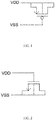
- Figures 1 and 2 respectively show a schematic diagram of the PMOS capacitance and the NMOS capacitance as a filter capacitance between the power supply and the ground.
- this filter circuit only has a capacitive characteristic, but does not have a ESD (Electro-Static discharge) characteristic.
- ESD Electro-Static discharge
- Some embodiments of the present application aim to provide a filter circuit based on MOS field effect transistors, and a chip including the filter circuit, so that the filter circuit can present a capacitance characteristic when the chip works normally, and provide a ESD path when an ESD event occurs between the power supply of the chip and the ground, and enhance the ESD capability of the chip.
- An embodiment of the present application provides a filter circuit based on MOS field effect transistors, including a first MOS field effect transistor and an electrostatic discharge unit; a filter capacitance is formed between a gate of the first MOS field effect transistor and a substrate during normal operation; the electrostatic discharge unit and the first MOS field effect transistor form a discharge path that transfers aggregated electrostatic charges to the ground during electrostatic discharge.
- An embodiment of the present application further provides a chip, including the filter circuit based on MOS field effect transistors as described above, the filter circuit is provided between the power supply of the chip and the ground.
- the embodiments of the present application as compared to the existing technology, add an electrostatic discharge unit on the basis of the first MOS field effect transistor, which combines the capacitance characteristic and the characteristic of the ESD discharge path needed between the power supply and the ground to the same circuit, so that the circuit presents the capacitance characteristic during normal operation, having a function of filtering AC interference in the power supply; and provides the ESD discharge path when an ESD event occurs between the power supply and the ground, which plays the role of ESD protection, and is favorable to the enhancement of the ESD capability of the chip.
- the electrostatic discharge unit includes a second MOS field effect transistor and a third MOS field effect transistor; a drain of the first MOS field effect transistor, a drain of the second MOS field effect transistor and a drain of the third MOS field effect transistor are interconnected; a gate of the first MOS field effect transistor, a gate of the second MOS field effect transistor and a gate of the third MOS field effect transistor are all grounded; a source of the first MOS field effect transistor with the substrate and a source of the second MOS field effect transistor with the substrate are connected to a power supply; and a source of the third MOS field effect transistor with the substrate is grounded.
- a form of an electrostatic discharge unit and its connection structure with the first MOS field effect transistor are provided.
- the first MOS field effect transistor is a PMOS field effect transistor
- the second MOS field effect transistor is a PMOS field effect transistor
- the third MOS field effect transistor is a NMOS field effect transistor.
- a type of the first MOS field effect transistor, second MOS field effect transistor and third MOS field effect transistor is provided.
- the gate of the second MOS field effect transistor is connected to the gate of the third MOS field effect transistor and then is grounded through a resistance. Connecting a resistance in series at a gate makes the Snap-back easier to turn on, making it easier to play the role of ESD protection.
- the electrostatic discharge unit includes the second MOS field effect transistor and the third MOS field effect transistor; the drain of the first MOS field effect transistor, the drain of the second MOS field effect transistor and the drain of the third MOS field effect transistor are interconnected; the gate of the first MOS field effect transistor, the gate of the second MOS field effect transistor, and the gate of the third MOS field effect transistor are all connected to the power supply; the source of the first MOS field effect transistor with the substrate and the source of the third MOS field effect transistor with the substrate are grounded; and the source of the second MOS field effect transistor with the substrate is connected to the power supply.
- Another connection structure of the electrostatic discharge unit with the first MOS field effect transistor is provided.
- the first MOS field effect transistor is a NMOS field effect transistor
- the second MOS field effect transistor is a PMOS field effect transistor
- the third MOS field effect transistor is still a NMOS field effect transistor. Another type of the first MOS field effect transistor is provided.
- the gate of the second MOS field effect transistor is connected to the gate of the third MOS field-effect transistor and then is connected to the power supply through a resistance. Connecting a resistance in series at a gate makes the Snap-back easier to turn on, making it easier to play the role of ESD protection.
- the overall size of the first MOS field effect transistor is greater than the overall size of the second MOS field effect transistor; and the overall size of the first MOS field effect transistor is greater than the overall size of the third MOS field effect transistor.
- the drain and the source of the third MOS field effect transistor there is a parasitic triode between the drain and the source of the third MOS field effect transistor, and there is a parasitic resistance between a base of the parasitic triode and the substrate of the third MOS field effect transistor.
- a reverse PN junction between the drain of the third MOS field effect transistor and the substrate breaks down, and a current flows to the base of the parasitic triode and to the ground through the parasitic resistance, so that the base voltage of the parasitic triode is raised and the parasitic triode is turned on and a low-impedance discharge path is formed.
- the discharge path provides a path for the aggregated electrostatic charges to be quickly discharged to the ground.
- the drain and the source of the second MOS field effect transistor there is a parasitic triode between the drain and the source of the second MOS field effect transistor, and there is a parasitic resistance between a base of the parasitic triode and a substrate of the second MOS field effect transistor.
- the reverse PN junction between the substrate and the drain of the second MOS field effect transistor breaks down, and a current flows to the base of the parasitic triode and to the drain through the parasitic resistance, so that the base voltage of the parasitic triode drops and the parasitic triode is turned on and a low-impedance discharge path is formed.
- the discharge path provides a path for the aggregated electrostatic charges to be quickly discharged to the drain.
- a first embodiment of the application relates to a filter circuit that is based on a MOS field effect transistor.
- the filter circuit includes a first MOS field effect transistor and an electrostatic discharge unit.
- the electrostatic discharge unit may be composed of multiple MOS field effect transistors, and cooperates with the first MOS field effect transistor so that a MOS capacitance can be formed as a filter capacitance between a gate of the first MOS field effect transistor and a substrate during normal operation, so that the filter circuit presents a capacitance characteristic.
- the electrostatic discharge unit can provide a low-impedance discharge path and transfer the aggregated electrostatic charges to the ground to achieve a goal of ESD protection.
- the electrostatic discharge unit may be composed of two MOS field effect transistors, i.e., a second MOS field effect transistor and a third MOS field effect transistors, respectively.
- a second MOS field effect transistor Taken the first MOS field effect transistor as a PMOS field effect transistor, the second MOS field effect transistor as a PMOS field effect transistor and the third MOS field effect transistor as a NMOS field effect transistor as an example, the connection structure of the first MOS field effect transistor and the electrostatic discharge unit is explained in detail in this embodiment.
- a drain of a first MOS field effect transistor M1 As illustrated in FIG. 3 , a drain of a first MOS field effect transistor M1, a drain of a second MOS field effect transistor M2 and a drain of a third MOS field effect transistor M3 are interconnected (a point of connection of the three marked as A in FIG.
- a gate of the first MOS field effect transistor M1 is connected to ground VSS, and a gate of the second MOS field effect transistor M2 and a gate of the third MOS field effect transistor M3 are interconnected and then connected to the ground VSS together; a source of the first MOS field effect transistor M1 with the substrate and a source of the second MOS field effect transistor M2 with the substrate are connected to a power supply VDD, and a source of the third MOS field effect transistor M3 with the substrate is connected to the ground VSS.
- the third MOS field-effect transistor M3 is in an OFF state. In this case, the drain and the source of the third MOS field effect transistor M3 are in a disconnection state. While, the second MOS field-effect transistor M2 is in an ON state, therefore, the drain of the first MOS field effect transistor M1 can be connected to the power supply VDD via the second MOS field effect transistor M2. Accordingly, during normal operation, the equivalent circuit in FIG. 3 is the same as that in FIG. 1 , and its function is also the same as that in FIG. 1 . That is, a PMOS capacitance is formed between the gate of the first MOS field effect transistor M1 and the substrate (N type substrate), and is used as a filter capacitance to filter AC interference in the power supply. That is to say, during normal operation, the filter circuit provided by this embodiment presents the capacitance characteristic.
- the overall size of the first MOS field effect transistor M1 is much larger than the other two MOS field effect transistors (i.e. the second MOS field effect transistor M2 and the third MOS field effect transistor M3). Because the greater the size is, the less the impedance is, an impedance of the first MOS field effect transistor M1 is much smaller than that of the other two MOS field-effect transistors. So, when an ESD event occurs between the power supply and the ground, most of the charges from the power supply will reach the drain from the source of the first MOS field effect transistor M1, i.e., the point A, and are aggregated here. With an increase in electrostatic charges (i.e.
- the filter circuit in this embodiment can provide a low-impedance discharge path.
- FIG. 4 shows a sectional structure of the third MOS field effect transistor M3, where there is a parasitic triode (NPN type) between a drain (D) and a source (S), and there is a parasitic resistance R between the base of the parasitic triode and the substrate of the third MOS field effect transistor.
- NPN type parasitic triode
- S source
- R parasitic resistance
- the current will flow to the base of the parasitic transistor and flow to the terminal B (i.e., the ground VSS) through the parasitic resistance R, which raises a base voltage of the parasitic triode and turns the parasitic triode on, thereby enabling Snap-back to form a low-impedance discharge path.
- the aggregated electrostatic charge can be quickly discharged to the ground through the low-impedance discharge path.
- the breakover uniformity (also known as enabling uniformity) of the third MOS field effect transistor M3 can affect the performance of its electrostatic protection.
- an electrostatic discharge unit is added on the basis of the first MOS field effect transistor.
- This design combines the capacitance characteristic and the characteristic of the ESD discharge path needed between the power supply and the ground to the same circuit, so that the circuit presents the capacitance characteristic during normal operation and plays the role of filtering AC interference in the power supply; an ESD discharge path is provided when an ESD event occurs between the power supply and the ground, which plays the role of ESD protection and is favorable for enhancing the ESD capability of the chip.
- a second embodiment of the present application relates to a filter circuit that is based on a MOS field effect transistor. On the basis of the first embodiment, this embodiment further improves the structure of the filter circuit.
- the main improvement mainly lies in that in this embodiment, the gate of the second MOS field effect transistor is connected to the gate of the third MOS field effect transistor and is then connected to the ground VSS through a resistance.
- the gate of the second MOS field-effect transistor M2 is connected to the gate of the third MOS field effect transistor M3 and then connected to the ground VSS through a resistance R0.
- the connection resistance R0 enables electrostatic charges to be coupled from the parasitic capacitance to the resistance R0, so that the third MOS field effect transistor M3 is in a weak conduction state when an ESD event occurs. In this case, the voltage for enabling Snap-back will be reduced, and it will more easily trigger the third MOS field effect transistor M3 to enable Snap-back.
- this embodiment reduces the voltage for enabling the Snap-back of the third MOS field effect transistor, making it easier to trigger the parasitic triode of the third MOS field effect transistor to turn on when an ESD event occurs to form a low-impedance discharge path, which is favorable to the improvement of the charge discharge capacity.
- a third embodiment of the present application relates to a filter circuit based on a MOS field effect transistor.
- the present embodiment can be used as an alternative embodiment of the first embodiment, and the difference between the two is that in the first embodiment, description is made when it is taken as an example that the first MOS field effect transistor is a PMOS field effect transistor, while in this embodiment, description is made when it is taken as an example that the first MOS field effect transistor is a NMOS field effect transistor.
- the connection structure of the three is as follows:
- a drain of the first MOS field effect transistor M1, a drain of the second MOS field effect transistor M2 and a drain of the third MOS field effect transistor M3 are interconnected (a point of connection of the three marked as A).
- a gate of the first MOS field effect transistor M1 is connected to the power supply VDD
- a gate of the second MOS field effect transistor M2 and a gate of the third MOS field effect transistor M3 are interconnected and then connected to the power supply VDD.
- a source of the first MOS field effect transistor M1 with the substrate and a source of the third MOS field effect transistor M3 with the substrate are connected to the ground VSS; and a source of the second MOS field effect transistor M2 with the substrate is connected to the power supply VDD.
- the second MOS field effect transistor M2 is in an OFF state.
- the drain and the source of the second MOS field effect transistor M2 are equivalent to be in a disconnection state.
- the third MOS field effect transistor M3 is in an ON state. Therefore, the drain of the first MOS field effect transistor M1 can be connected to the ground VSS via the third MOS field effect transistor M3.
- the equivalent circuit in FIG. 5 is the same as that in FIG. 2 , and its function is also the same as that in FIG. 2 . That is, a NMOS capacitance is formed between the gate of the first MOS field effect transistor M1 and the substrate, which is used as a filter capacitance to filter AC interference in the power supply. That is to say, during normal operation, the filter circuit provided by this embodiment presents the capacitance characteristic.
- the electrostatic charges aggregated at the source of the second MOS field effect transistor M2 will raise the voltage at that point.
- the voltage at this point is raised to a certain value (voltage value at which Snap-back is enabled)
- it will trigger the second MOS field effect transistor M2 to enable Snap-back, that is, to trigger the parasitic triode of the second MOS field-effect transistor M2 to turn on and form a low-impedance discharge path.
- the aggregated electrostatic charges can be discharged to the point A through the low-impedance discharge path.
- parasitic triode PNP type
- parasitic resistance between the base of the parasitic triode and the substrate of the second MOS field effect transistor.
- the overall size of the first MOS field effect transistor M1 is still much greater than the overall size of the other two MOS field effect transistors, that is to say, the impedance of the first MOS field effect transistor M1 is much smaller than the impedances of the other two MOS field effect transistors. Therefore, after the charges are discharged to the point A, a large majority of the charges will flow to the source of the first MOS field effect transistor M1, and then from the source of the first MOS field effect transistor M1 to the ground VSS (an arrow in FIG. 6 shows the transfer path of the large majority of the charges during the electrostatic discharge); only a small amount of them will flow to the source of the third MOS field effect transistor M3 and then to the ground VSS. Being compared to the previous part, the latter amount may substantially be neglected.
- this embodiment provides another type of the first MOS field effect transistor M1, as well as a connection structure between the electrostatic discharge unit and the first MOS field effect transistor.
- a fourth embodiment of the present application relates to a filter circuit that is based on a MOS field effect transistor. Based on the third embodiment, this embodiment further improves the structure of the filter circuit. The main improvement is that in this embodiment, the gate of the second MOS field effect transistor is connected to the gate of the third MOS field effect transistor and is then connected to the power VDD through a resistance.
- the gate of the third MOS field effect transistor M3 is connected to the gate of the second MOS field effect transistor M2, and is then connected to the power supply VDD through the resistance R1.
- the connection resistance R1 enables the second MOS field effect transistor to be in a weak conduction state when an ESD event occurs, thereby reducing the value of voltage for enabling Snap-back of the second MOS field effect transistor, so that it is easier to enable the Snap-back of the second MOS field effect transistor.
- this designed structure makes it possible to trigger the parasitic triode of the second MOS field effect transistor to turn on more easily and faster when an ESD event occurs, so as to form a low-impedance discharge path (an arrow in FIG. 7 shows the transfer path of a large majority of the charges during electrostatic discharge), which quickly discharges the aggregated electrostatic charges to the ground. This is favorable for the improvement of the ESD capability of the chip to better protect the components inside the chip.
- this embodiment reduces the voltage for enabling the Snap-back of the second MOS field effect transistor, making it possible to trigger the parasitic triode of the second MOS field effect transistor to turn on more easily and faster when an ESD event occurs, so as to form a low-impedance discharge path, which is favorable for the improvement of the ability of charge discharge.
- a fifth embodiment of the application relates to a chip.
- the chip includes a filter circuit that is based on a MOS field effect transistor described in the above embodiments, the filter circuit is located between the power supply of the chip and the ground.
- the filter circuit When the chip is working normally, the filter circuit presents the capacitance characteristic; when an ESD event occurs between the power supply of the chip and the ground, the filter circuit provides a low-impedance discharge path to discharge the aggregated electrostatic charges to the ground, thereby preventing the internal components of the chip from being damaged by overvoltage.
- an electrostatic discharge unit on the basis of the first MOS field effect transistor, which combines the capacitance characteristic and the characteristic of the ESD discharge path needed between the power and the ground to the same circuit, so that the chip presents the capacitance characteristic during normal operation.
- a low-impedance ESD discharge path is provided between the power supply of the chip and the ground, which plays the role of ESD protection.
Landscapes
- Engineering & Computer Science (AREA)
- Microelectronics & Electronic Packaging (AREA)
- Semiconductor Integrated Circuits (AREA)
- Metal-Oxide And Bipolar Metal-Oxide Semiconductor Integrated Circuits (AREA)
Abstract
Description
- The present application relates to integrated circuit technologies and, more particularly, to a filter circuit based on a MOS field effect transistor and a chip including the same.
- In general, during finishing process of a chip design, a filter circuit between a power supply and ground is added to a spare part of the chip. A chosen filter capacitance can be a MOS (Metal-Oxide-Semiconductor) field effect transistor capacitance, a MIM (Metal-Insulator-Metal) capacitance, or a MOM (Metal-Oxide-Metal) capacitance and the like. However, considering that a per-unit-area capacitance of the MOS field effect transistor capacitance (hereinafter referred to as a MOS capacitance) is greater than any other capacitance, a greater capacitance can be obtained under the same area. Therefore, in general, the MOS capacitance is selected as a filter capacitance.
- The MOS capacitance is categorized into two types: a PMOS capacitance and a NMOS capacitance.
Figures 1 and 2 respectively show a schematic diagram of the PMOS capacitance and the NMOS capacitance as a filter capacitance between the power supply and the ground. In general, this filter circuit only has a capacitive characteristic, but does not have a ESD (Electro-Static discharge) characteristic. In practical applications, however, ESD events often occur between the power supply and the ground, threatening security of the components inside the chip. Therefore, it is very important to enhance the ESD capability of the chip. - Some embodiments of the present application aim to provide a filter circuit based on MOS field effect transistors, and a chip including the filter circuit, so that the filter circuit can present a capacitance characteristic when the chip works normally, and provide a ESD path when an ESD event occurs between the power supply of the chip and the ground, and enhance the ESD capability of the chip.
- An embodiment of the present application provides a filter circuit based on MOS field effect transistors, including a first MOS field effect transistor and an electrostatic discharge unit; a filter capacitance is formed between a gate of the first MOS field effect transistor and a substrate during normal operation; the electrostatic discharge unit and the first MOS field effect transistor form a discharge path that transfers aggregated electrostatic charges to the ground during electrostatic discharge.
- An embodiment of the present application further provides a chip, including the filter circuit based on MOS field effect transistors as described above, the filter circuit is provided between the power supply of the chip and the ground.
- The embodiments of the present application, as compared to the existing technology, add an electrostatic discharge unit on the basis of the first MOS field effect transistor, which combines the capacitance characteristic and the characteristic of the ESD discharge path needed between the power supply and the ground to the same circuit, so that the circuit presents the capacitance characteristic during normal operation, having a function of filtering AC interference in the power supply; and provides the ESD discharge path when an ESD event occurs between the power supply and the ground, which plays the role of ESD protection, and is favorable to the enhancement of the ESD capability of the chip.
- Also, the electrostatic discharge unit includes a second MOS field effect transistor and a third MOS field effect transistor; a drain of the first MOS field effect transistor, a drain of the second MOS field effect transistor and a drain of the third MOS field effect transistor are interconnected; a gate of the first MOS field effect transistor, a gate of the second MOS field effect transistor and a gate of the third MOS field effect transistor are all grounded; a source of the first MOS field effect transistor with the substrate and a source of the second MOS field effect transistor with the substrate are connected to a power supply; and a source of the third MOS field effect transistor with the substrate is grounded. A form of an electrostatic discharge unit and its connection structure with the first MOS field effect transistor are provided.
- Also, the first MOS field effect transistor is a PMOS field effect transistor, the second MOS field effect transistor is a PMOS field effect transistor, and the third MOS field effect transistor is a NMOS field effect transistor. A type of the first MOS field effect transistor, second MOS field effect transistor and third MOS field effect transistor is provided.
- Also, the gate of the second MOS field effect transistor is connected to the gate of the third MOS field effect transistor and then is grounded through a resistance. Connecting a resistance in series at a gate makes the Snap-back easier to turn on, making it easier to play the role of ESD protection.
- Also, the electrostatic discharge unit includes the second MOS field effect transistor and the third MOS field effect transistor; the drain of the first MOS field effect transistor, the drain of the second MOS field effect transistor and the drain of the third MOS field effect transistor are interconnected; the gate of the first MOS field effect transistor, the gate of the second MOS field effect transistor, and the gate of the third MOS field effect transistor are all connected to the power supply; the source of the first MOS field effect transistor with the substrate and the source of the third MOS field effect transistor with the substrate are grounded; and the source of the second MOS field effect transistor with the substrate is connected to the power supply. Another connection structure of the electrostatic discharge unit with the first MOS field effect transistor is provided.
- Also, the first MOS field effect transistor is a NMOS field effect transistor, the second MOS field effect transistor is a PMOS field effect transistor, and the third MOS field effect transistor is still a NMOS field effect transistor. Another type of the first MOS field effect transistor is provided.
- Also, the gate of the second MOS field effect transistor is connected to the gate of the third MOS field-effect transistor and then is connected to the power supply through a resistance. Connecting a resistance in series at a gate makes the Snap-back easier to turn on, making it easier to play the role of ESD protection.
- Also, the overall size of the first MOS field effect transistor is greater than the overall size of the second MOS field effect transistor; and the overall size of the first MOS field effect transistor is greater than the overall size of the third MOS field effect transistor. The greater the size is, the less the impedance is. This designed structure enables the first MOS field effect transistor to transfer more electrostatic charges to the ground, which helps to enhance the capacity of the ESD charge discharge.
- Also, there is a parasitic triode between the drain and the source of the third MOS field effect transistor, and there is a parasitic resistance between a base of the parasitic triode and the substrate of the third MOS field effect transistor. When a large amount of charges are aggregated at the drain of the third MOS field effect transistor, a reverse PN junction between the drain of the third MOS field effect transistor and the substrate breaks down, and a current flows to the base of the parasitic triode and to the ground through the parasitic resistance, so that the base voltage of the parasitic triode is raised and the parasitic triode is turned on and a low-impedance discharge path is formed. The discharge path provides a path for the aggregated electrostatic charges to be quickly discharged to the ground.
- Also, there is a parasitic triode between the drain and the source of the second MOS field effect transistor, and there is a parasitic resistance between a base of the parasitic triode and a substrate of the second MOS field effect transistor. When a large amount of charges are aggregated at the source of the second MOS field effect transistor, the reverse PN junction between the substrate and the drain of the second MOS field effect transistor breaks down, and a current flows to the base of the parasitic triode and to the drain through the parasitic resistance, so that the base voltage of the parasitic triode drops and the parasitic triode is turned on and a low-impedance discharge path is formed. The discharge path provides a path for the aggregated electrostatic charges to be quickly discharged to the drain.
- One or more embodiments are exemplified by the figures in the accompanying drawings, which is not a limit to the embodiments. Elements with the same reference numerals in the drawings are represented as similar elements. Unless otherwise stated, the figures in the drawings do not constitute a proportional limitation.
-
FIG. 1 is a schematic diagram of a circuit with a PMOS field effect transistor as a filter capacitance in the existing technology; -
FIG. 2 is a schematic diagram of a circuit with a NMOS field effect transistor as a filter capacitance in the existing technology; -
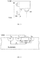
FIG. 3 is a schematic diagram of a filter circuit based on MOS field effect transistors according to a first embodiment of the application; -
FIG. 4 is a sectional schematic diagram of a third MOS field effect transistor M3 according to the first embodiment of the application; -
FIG. 5 is a schematic diagram of a filter circuit based on MOS field effect transistors according to a second embodiment of the application; -
FIG. 6 is a schematic diagram of a filter circuit based on MOS field effect transistors according to a third embodiment of the application; -
FIG. 7 is a schematic diagram of a filter circuit based on MOS field effect transistors according to a fourth embodiment of the application. - In order to make the purposes, the technical solutions and the advantages of this application clearer, some embodiments of the present application will be explained below in further detail with reference to the accompanying drawings and embodiments. It should be understood that the specific embodiments described herein only explain the application but do not limit the application.
- A first embodiment of the application relates to a filter circuit that is based on a MOS field effect transistor. The filter circuit includes a first MOS field effect transistor and an electrostatic discharge unit.
- The electrostatic discharge unit may be composed of multiple MOS field effect transistors, and cooperates with the first MOS field effect transistor so that a MOS capacitance can be formed as a filter capacitance between a gate of the first MOS field effect transistor and a substrate during normal operation, so that the filter circuit presents a capacitance characteristic. When an ESD event occurs between a power supply and ground, the electrostatic discharge unit can provide a low-impedance discharge path and transfer the aggregated electrostatic charges to the ground to achieve a goal of ESD protection.
- Preferably, the electrostatic discharge unit may be composed of two MOS field effect transistors, i.e., a second MOS field effect transistor and a third MOS field effect transistors, respectively. Taken the first MOS field effect transistor as a PMOS field effect transistor, the second MOS field effect transistor as a PMOS field effect transistor and the third MOS field effect transistor as a NMOS field effect transistor as an example, the connection structure of the first MOS field effect transistor and the electrostatic discharge unit is explained in detail in this embodiment.
- As illustrated in
FIG. 3 , a drain of a first MOS field effect transistor M1, a drain of a second MOS field effect transistor M2 and a drain of a third MOS field effect transistor M3 are interconnected (a point of connection of the three marked as A inFIG. 3 ); a gate of the first MOS field effect transistor M1 is connected to ground VSS, and a gate of the second MOS field effect transistor M2 and a gate of the third MOS field effect transistor M3 are interconnected and then connected to the ground VSS together; a source of the first MOS field effect transistor M1 with the substrate and a source of the second MOS field effect transistor M2 with the substrate are connected to a power supply VDD, and a source of the third MOS field effect transistor M3 with the substrate is connected to the ground VSS. - During normal operation, the third MOS field-effect transistor M3 is in an OFF state. In this case, the drain and the source of the third MOS field effect transistor M3 are in a disconnection state. While, the second MOS field-effect transistor M2 is in an ON state, therefore, the drain of the first MOS field effect transistor M1 can be connected to the power supply VDD via the second MOS field effect transistor M2. Accordingly, during normal operation, the equivalent circuit in
FIG. 3 is the same as that inFIG. 1 , and its function is also the same as that inFIG. 1 . That is, a PMOS capacitance is formed between the gate of the first MOS field effect transistor M1 and the substrate (N type substrate), and is used as a filter capacitance to filter AC interference in the power supply. That is to say, during normal operation, the filter circuit provided by this embodiment presents the capacitance characteristic. - It is worth mentioning that, in this embodiment, the overall size of the first MOS field effect transistor M1 is much larger than the other two MOS field effect transistors (i.e. the second MOS field effect transistor M2 and the third MOS field effect transistor M3). Because the greater the size is, the less the impedance is, an impedance of the first MOS field effect transistor M1 is much smaller than that of the other two MOS field-effect transistors. So, when an ESD event occurs between the power supply and the ground, most of the charges from the power supply will reach the drain from the source of the first MOS field effect transistor M1, i.e., the point A, and are aggregated here. With an increase in electrostatic charges (i.e. charges aggregated at the point A), the voltage at the point A will be raised. When the voltage at this point is raised to a certain value (voltage value at which Snap-back is enabled), the third MOS field effect transistor M3 will be triggered to enable Snap-back, that is, a parasitic triode of the third MOS field effect transistor M3 will be triggered to turn on and a low-impedance discharge path is formed. The aggregated electrostatic charges can be discharged to the ground VSS through the low-impedance discharge path (an arrow in
FIG. 3 shows the transfer path of a large majority of the charges during the electrostatic discharge) so as to protect internal components of the chip. That is to say, when an ESD event occurs between the power supply and the ground, the filter circuit in this embodiment can provide a low-impedance discharge path. - It is to be explained in the following on how the third MOS field-effect transistor M3 discharges electrostatic charges aggregated at the drain to the ground VSS.
-
FIG. 4 shows a sectional structure of the third MOS field effect transistor M3, where there is a parasitic triode (NPN type) between a drain (D) and a source (S), and there is a parasitic resistance R between the base of the parasitic triode and the substrate of the third MOS field effect transistor. When a large number of charges are aggregated at the drain, the reverse PN junction between the drain and the substrate (P-substrate) will break down. At this time, the current will flow to the base of the parasitic transistor and flow to the terminal B (i.e., the ground VSS) through the parasitic resistance R, which raises a base voltage of the parasitic triode and turns the parasitic triode on, thereby enabling Snap-back to form a low-impedance discharge path. The aggregated electrostatic charge can be quickly discharged to the ground through the low-impedance discharge path. - It is worth noted that in the ESD protection, the breakover uniformity (also known as enabling uniformity) of the third MOS field effect transistor M3 can affect the performance of its electrostatic protection. In design, it is possible to increase the breakover uniformity by appropriately increasing a width of the drain (which is equivalent to increasing the resistance in the circuit and thereby reducing the current), thereby improving its ability of electrostatic discharge.
- As compared to the existing technologies, in this embodiment, an electrostatic discharge unit is added on the basis of the first MOS field effect transistor. This design combines the capacitance characteristic and the characteristic of the ESD discharge path needed between the power supply and the ground to the same circuit, so that the circuit presents the capacitance characteristic during normal operation and plays the role of filtering AC interference in the power supply; an ESD discharge path is provided when an ESD event occurs between the power supply and the ground, which plays the role of ESD protection and is favorable for enhancing the ESD capability of the chip.
- A second embodiment of the present application relates to a filter circuit that is based on a MOS field effect transistor. On the basis of the first embodiment, this embodiment further improves the structure of the filter circuit. The main improvement mainly lies in that in this embodiment, the gate of the second MOS field effect transistor is connected to the gate of the third MOS field effect transistor and is then connected to the ground VSS through a resistance.
- As shown in
Fig. 5 , the gate of the second MOS field-effect transistor M2 is connected to the gate of the third MOS field effect transistor M3 and then connected to the ground VSS through a resistance R0. There is a parasitic capacitance between the gate (G) and the drain (D) of the third MOS field effect transistor M3. The connection resistance R0 enables electrostatic charges to be coupled from the parasitic capacitance to the resistance R0, so that the third MOS field effect transistor M3 is in a weak conduction state when an ESD event occurs. In this case, the voltage for enabling Snap-back will be reduced, and it will more easily trigger the third MOS field effect transistor M3 to enable Snap-back. That is, when an ESD event occurs, the conduction of the parasitic triode of the third MOS field effect transistor can be triggered more easily and faster to form a low-impedance discharge path (an arrow inFigure 5 shows a transfer path of a large majority of the charges upon electrostatic discharge), so that the aggregated electrostatic charges are quickly discharged to the ground, which is favorable for improving charge discharge ability of the chip and enhancing protection over components inside the chip. - In comparison with the first embodiment, this embodiment reduces the voltage for enabling the Snap-back of the third MOS field effect transistor, making it easier to trigger the parasitic triode of the third MOS field effect transistor to turn on when an ESD event occurs to form a low-impedance discharge path, which is favorable to the improvement of the charge discharge capacity.
- A third embodiment of the present application relates to a filter circuit based on a MOS field effect transistor. The present embodiment can be used as an alternative embodiment of the first embodiment, and the difference between the two is that in the first embodiment, description is made when it is taken as an example that the first MOS field effect transistor is a PMOS field effect transistor, while in this embodiment, description is made when it is taken as an example that the first MOS field effect transistor is a NMOS field effect transistor.
- When the first MOS field effect transistor M1 is a NMOS field effect transistor, the second MOS field effect transistor M2 is still a PMOS field effect transistor and the third MOS field effect transistor M3 is still a NMOS field effect transistor, the connection structure of the three is as follows:
- As shown in
FIG. 6 , a drain of the first MOS field effect transistor M1, a drain of the second MOS field effect transistor M2 and a drain of the third MOS field effect transistor M3 are interconnected (a point of connection of the three marked as A). A gate of the first MOS field effect transistor M1 is connected to the power supply VDD, a gate of the second MOS field effect transistor M2 and a gate of the third MOS field effect transistor M3 are interconnected and then connected to the power supply VDD. A source of the first MOS field effect transistor M1 with the substrate and a source of the third MOS field effect transistor M3 with the substrate are connected to the ground VSS; and a source of the second MOS field effect transistor M2 with the substrate is connected to the power supply VDD. - During normal operation, the second MOS field effect transistor M2 is in an OFF state. In this case, the drain and the source of the second MOS field effect transistor M2 are equivalent to be in a disconnection state. The third MOS field effect transistor M3 is in an ON state. Therefore, the drain of the first MOS field effect transistor M1 can be connected to the ground VSS via the third MOS field effect transistor M3. In this case, the equivalent circuit in
FIG. 5 is the same as that inFIG. 2 , and its function is also the same as that inFIG. 2 . That is, a NMOS capacitance is formed between the gate of the first MOS field effect transistor M1 and the substrate, which is used as a filter capacitance to filter AC interference in the power supply. That is to say, during normal operation, the filter circuit provided by this embodiment presents the capacitance characteristic. - When an ESD event occurs between the power supply and the ground, the electrostatic charges aggregated at the source of the second MOS field effect transistor M2 will raise the voltage at that point. When the voltage at this point is raised to a certain value (voltage value at which Snap-back is enabled), it will trigger the second MOS field effect transistor M2 to enable Snap-back, that is, to trigger the parasitic triode of the second MOS field-effect transistor M2 to turn on and form a low-impedance discharge path. As a result, the aggregated electrostatic charges can be discharged to the point A through the low-impedance discharge path.
- Specifically, there is a parasitic triode (PNP type) between the drain and the source of the second MOS field effect transistor, and there is a parasitic resistance between the base of the parasitic triode and the substrate of the second MOS field effect transistor. When a large number of charges are aggregated at the source of the second MOS field effect transistor, the reverse PN junction between the substrate and the drain of the second MOS field effect transistor breaks down. At this time, the current flows to the base of the parasitic triode, and to the drain (the point A) through the parasitic resistance, which reduces the base voltage of the parasitic triode, turns on the parasitic triode, and enables Snap-back, so that a low-impedance discharge path is formed. The aggregated electrostatic charges can be quickly discharged to the point A through the low-impedance discharge path.
- Similarly, in this embodiment, the overall size of the first MOS field effect transistor M1 is still much greater than the overall size of the other two MOS field effect transistors, that is to say, the impedance of the first MOS field effect transistor M1 is much smaller than the impedances of the other two MOS field effect transistors. Therefore, after the charges are discharged to the point A, a large majority of the charges will flow to the source of the first MOS field effect transistor M1, and then from the source of the first MOS field effect transistor M1 to the ground VSS (an arrow in
FIG. 6 shows the transfer path of the large majority of the charges during the electrostatic discharge); only a small amount of them will flow to the source of the third MOS field effect transistor M3 and then to the ground VSS. Being compared to the previous part, the latter amount may substantially be neglected. - As compared to the first embodiment, this embodiment provides another type of the first MOS field effect transistor M1, as well as a connection structure between the electrostatic discharge unit and the first MOS field effect transistor.
- A fourth embodiment of the present application relates to a filter circuit that is based on a MOS field effect transistor. Based on the third embodiment, this embodiment further improves the structure of the filter circuit. The main improvement is that in this embodiment, the gate of the second MOS field effect transistor is connected to the gate of the third MOS field effect transistor and is then connected to the power VDD through a resistance.
- As shown in
FIG. 7 , the gate of the third MOS field effect transistor M3 is connected to the gate of the second MOS field effect transistor M2, and is then connected to the power supply VDD through the resistance R1. Similarly, the connection resistance R1 enables the second MOS field effect transistor to be in a weak conduction state when an ESD event occurs, thereby reducing the value of voltage for enabling Snap-back of the second MOS field effect transistor, so that it is easier to enable the Snap-back of the second MOS field effect transistor. In other words, this designed structure makes it possible to trigger the parasitic triode of the second MOS field effect transistor to turn on more easily and faster when an ESD event occurs, so as to form a low-impedance discharge path (an arrow inFIG. 7 shows the transfer path of a large majority of the charges during electrostatic discharge), which quickly discharges the aggregated electrostatic charges to the ground. This is favorable for the improvement of the ESD capability of the chip to better protect the components inside the chip. - As compared to the first embodiment, this embodiment reduces the voltage for enabling the Snap-back of the second MOS field effect transistor, making it possible to trigger the parasitic triode of the second MOS field effect transistor to turn on more easily and faster when an ESD event occurs, so as to form a low-impedance discharge path, which is favorable for the improvement of the ability of charge discharge.
- A fifth embodiment of the application relates to a chip. The chip includes a filter circuit that is based on a MOS field effect transistor described in the above embodiments, the filter circuit is located between the power supply of the chip and the ground.
- When the chip is working normally, the filter circuit presents the capacitance characteristic; when an ESD event occurs between the power supply of the chip and the ground, the filter circuit provides a low-impedance discharge path to discharge the aggregated electrostatic charges to the ground, thereby preventing the internal components of the chip from being damaged by overvoltage.
- As compared to the existing technologies, it is added to this embodiment an electrostatic discharge unit on the basis of the first MOS field effect transistor, which combines the capacitance characteristic and the characteristic of the ESD discharge path needed between the power and the ground to the same circuit, so that the chip presents the capacitance characteristic during normal operation. When an ESD event occurs, a low-impedance ESD discharge path is provided between the power supply of the chip and the ground, which plays the role of ESD protection.
- Those ordinarily skilled in the art can understand that the above-mentioned embodiments are specific embodiments of implementing this application. In practical applications, various changes can be made in form and in detail without deviating from the spirit and scope of the application.
Claims (11)
- A filter circuit that is based on a MOS field effect transistor, characterized by comprising a first MOS field effect transistor and an electrostatic discharge unit;
wherein a gate of the first MOS field effect transistor and a substrate form a filter capacitance during normal operation;
wherein the electrostatic discharge unit and the first MOS field effect transistor form a discharge path that transfers aggregated electrostatic charges to ground during electrostatic discharge. - The filter circuit that is based on a MOS field effect transistor according to claim 1, characterized in that the electrostatic discharge unit comprises a second MOS field effect transistor and a third MOS field effect transistor;
a drain of the first MOS field effect transistor, a drain of the second MOS field effect transistor and a drain of the third MOS field effect transistor are interconnected; a gate of the first MOS field effect transistor, a gate of the second MOS field effect transistor and a gate of the third MOS field effect transistor are all grounded; a source of the first MOS field effect transistor with the substrate and a source of the second MOS field effect transistor with the substrate are connected to a power supply; and a source of the third MOS field effect transistor with the substrate is grounded. - The filter circuit that is based on a MOS field effect transistor according to claim 2, characterized in that the first MOS field effect transistor is a PMOS field effect transistor, the second MOS field effect transistor is a PMOS field effect transistor, and the third MOS field effect transistor is an NMOS field effect transistor.
- The filter circuit that is based on a MOS field effect transistor according to the claim 2, characterized in that the gate of the second MOS field effect transistor is connected to the gate of the third MOS field effect transistor and is then grounded through a resistance.
- The filter circuit that is based on a MOS field effect transistor according to claim 1, characterized in that the electrostatic discharge unit comprises a second MOS field effect transistor and a third MOS field effect transistor;
a drain of the first MOS field effect transistor, a drain of the second MOS field effect transistor and a drain of the third MOS field effect transistor are interconnected; a gate of the first MOS field effect transistor, a gate of the second MOS field effect transistor and a gate of the third MOS field effect transistor are all connected to a power supply; a source of the first MOS field effect transistor with the substrate and a source of the third MOS field effect transistor with the substrate are grounded; and a source of the second MOS field effect transistor with the substrate is grounded. - The filter circuit that is based on a MOS field effect transistor according to claim 5, characterized in that the first MOS field effect transistor is a NMOS field effect transistor, the second MOS field effect transistor is a PMOS field effect transistor, and the third MOS field effect transistor is a NMOS field effect transistor.
- The filter circuit that is based on a MOS field effect transistor according to the claim 5, characterized in that the gate of the second MOS field effect transistor is connected to the gate of the third MOS field effect transistor and is then connected to the power supply through a resistance.
- The filter circuit that is based on a MOS field effect transistor according to any one of claims 2 to 7, characterized in that the overall size of the first MOS field effect transistor is larger than the overall size of the second MOS field effect transistor; and the overall size of the first MOS field effect transistor is larger than the overall size of the third MOS field effect transistor.
- The filter circuit that is based on a MOS field effect transistor according to any one of claims 2 to 4, characterized in that there is a parasitic triode between the drain and the source of the third MOS field effect transistor, and there is a parasitic resistance between a base of the parasitic triode and the substrate of the third MOS field effect transistor; wherein when a large amount of charges are aggregated at the drain of the third MOS field effect transistor, the reverse PN junction between the drain of the third MOS field effect transistor and the substrate breaks down, and a current flows to the base of the parasitic triode and to the ground through the parasitic resistance, such that the base voltage of the parasitic triode is raised and the parasitic triode is turned on and a low-impedance discharge path is formed; the discharge path provides a path for the aggregated electrostatic charges to be quickly discharged to the ground.
- The filter circuit that is based on a MOS field effect transistor according to any one of claims 5 to 7, characterized in that there is a parasitic triode between the drain and the source of the second MOS field effect transistor, and there is a parasitic resistance between a base of the parasitic triode and the substrate of the second MOS field effect transistor; wherein when a large amount of charges are aggregated at the drain of the second MOS field effect transistor, the reverse PN junction between the drain of the second MOS field effect transistor and the substrate breaks down, and a current flows to the base of the parasitic triode and to the drain through the parasitic resistance, such that the base voltage of the parasitic triode drops and the parasitic triode is turned on and a low-impedance discharge path is formed; the discharge path provides a path for the aggregated electrostatic charges to be quickly discharged to the drain.
- A chip, characterized by comprising a filter circuit based on MOS field effect transistors according to any one of claims 1 to 10, the filter circuit is provided between a power supply of the chip and a ground.
Applications Claiming Priority (1)
| Application Number | Priority Date | Filing Date | Title |
|---|---|---|---|
| PCT/CN2017/088201 WO2018227409A1 (en) | 2017-06-14 | 2017-06-14 | Mos field effect transistor-based filter circuit and chip |
Publications (3)
| Publication Number | Publication Date |
|---|---|
| EP3447800A1 true EP3447800A1 (en) | 2019-02-27 |
| EP3447800A4 EP3447800A4 (en) | 2019-08-07 |
| EP3447800B1 EP3447800B1 (en) | 2022-01-26 |
Family
ID=60554206
Family Applications (1)
| Application Number | Title | Priority Date | Filing Date |
|---|---|---|---|
| EP17905914.2A Active EP3447800B1 (en) | 2017-06-14 | 2017-06-14 | Mos field effect transistor-based filter circuit and chip |
Country Status (4)
| Country | Link |
|---|---|
| US (1) | US10930643B2 (en) |
| EP (1) | EP3447800B1 (en) |
| CN (1) | CN107466426B (en) |
| WO (1) | WO2018227409A1 (en) |
Families Citing this family (3)
| Publication number | Priority date | Publication date | Assignee | Title |
|---|---|---|---|---|
| CN108649793B (en) * | 2018-06-07 | 2021-07-06 | 上海艾为电子技术股份有限公司 | DC/DC converter and electronic device with same |
| CN110262771B (en) * | 2019-05-09 | 2021-07-13 | 中国科学院微电子研究所 | A basic operation circuit based on MOS transistor and its extension circuit |
| CN114265038B (en) * | 2021-11-22 | 2024-02-09 | 电子科技大学 | High-precision switch type phase shifting unit with temperature compensation effect |
Family Cites Families (20)
| Publication number | Priority date | Publication date | Assignee | Title |
|---|---|---|---|---|
| TW518736B (en) * | 2001-09-06 | 2003-01-21 | Faraday Tech Corp | Gate-driven or gate-coupled electrostatic discharge protection circuit |
| US6934136B2 (en) * | 2002-04-24 | 2005-08-23 | Texas Instrument Incorporated | ESD protection of noise decoupling capacitors |
| TWI264106B (en) * | 2002-04-30 | 2006-10-11 | Winbond Electronics Corp | Static charge protection circuit of adopting gate-coupled MOSFET (metal-oxide-semiconductor field effect transistor) |
| JP4515822B2 (en) * | 2004-05-25 | 2010-08-04 | 株式会社東芝 | Electrostatic protection circuit and semiconductor integrated circuit device using the same |
| TWI281740B (en) * | 2004-09-08 | 2007-05-21 | Winbond Electronics Corp | Electrostatic discharge protection circuit |
| US7292421B2 (en) * | 2004-11-12 | 2007-11-06 | Texas Instruments Incorporated | Local ESD power rail clamp which implements switchable I/O decoupling capacitance function |
| TWI296439B (en) * | 2005-08-08 | 2008-05-01 | Silicon Integrated Sys Corp | Esd protection circuit |
| JP2007081019A (en) * | 2005-09-13 | 2007-03-29 | Oki Electric Ind Co Ltd | Semiconductor device |
| US8064175B2 (en) * | 2005-09-15 | 2011-11-22 | Rambus Inc. | Power supply shunt |
| CN1979842A (en) * | 2005-12-01 | 2007-06-13 | 上海华虹Nec电子有限公司 | Electrostatic discharging protection circuit triggered by lining-bottom |
| US7495878B2 (en) * | 2007-03-22 | 2009-02-24 | Bae Systems Information And Electronic Systems Integration Inc. | Decoupling capacitor control circuit and method for enhanced ESD performance |
| JP2008305852A (en) * | 2007-06-05 | 2008-12-18 | Toshiba Corp | Semiconductor device |
| US20110063762A1 (en) * | 2009-09-13 | 2011-03-17 | Tang-Lung Lee | Flash memory circuit with esd protection |
| JP2012253241A (en) * | 2011-06-03 | 2012-12-20 | Sony Corp | Semiconductor integrated circuit and manufacturing method of the same |
| US8804290B2 (en) * | 2012-01-17 | 2014-08-12 | Texas Instruments Incorporated | Electrostatic discharge protection circuit having buffer stage FET with thicker gate oxide than common-source FET |
| US8760828B2 (en) * | 2012-03-08 | 2014-06-24 | Taiwan Semiconductor Manufacturing Co., Ltd. | Electro-static discharge clamp (ESD) for NxVDD power rail |
| US9716381B2 (en) * | 2013-09-20 | 2017-07-25 | The Regents Of The University Of Michigan | Electrostatic discharge clamp circuit for ultra-low power applications |
| US9397090B1 (en) * | 2015-04-10 | 2016-07-19 | Macronix International Co., Ltd. | Semiconductor device |
| JP2017123374A (en) * | 2016-01-05 | 2017-07-13 | ソニー株式会社 | Semiconductor integrated circuit and control method of the same |
| JP7027176B2 (en) * | 2018-01-22 | 2022-03-01 | ラピスセミコンダクタ株式会社 | Semiconductor device |
-
2017
- 2017-06-14 EP EP17905914.2A patent/EP3447800B1/en active Active
- 2017-06-14 CN CN201780000480.3A patent/CN107466426B/en active Active
- 2017-06-14 WO PCT/CN2017/088201 patent/WO2018227409A1/en not_active Ceased
-
2018
- 2018-10-26 US US16/171,582 patent/US10930643B2/en active Active
Also Published As
| Publication number | Publication date |
|---|---|
| US20190067272A1 (en) | 2019-02-28 |
| US10930643B2 (en) | 2021-02-23 |
| WO2018227409A1 (en) | 2018-12-20 |
| CN107466426A (en) | 2017-12-12 |
| EP3447800A4 (en) | 2019-08-07 |
| CN107466426B (en) | 2021-03-16 |
| EP3447800B1 (en) | 2022-01-26 |
Similar Documents
| Publication | Publication Date | Title |
|---|---|---|
| US6469560B1 (en) | Electrostatic discharge protective circuit | |
| US7110228B2 (en) | Separated power ESD protection circuit and integrated circuit thereof | |
| US20210343702A1 (en) | Electrostatic discharge protection circuit | |
| US20130155556A1 (en) | Electrostatic discharge protection circuit and method for radio frequency semiconductor device | |
| JPH11135723A (en) | Cascode connection MOS ESD protection circuit for mixed voltage chip | |
| CN101944530B (en) | An ESD protection circuit with a control circuit for an integrated circuit | |
| US7719813B2 (en) | Gate-coupled substrate-triggered ESD protection circuit and integrated circuit therewith | |
| US10930643B2 (en) | Filter circuit based on a MOS field effect transistor and chip including the same | |
| US20080151446A1 (en) | Electrostatic discharge protection device and layout thereof | |
| US8009399B2 (en) | ESD improvement with dynamic substrate resistance | |
| CN108878416A (en) | ESD protection circuit | |
| US7538998B2 (en) | Electrostatic discharge protection circuit | |
| KR20110082265A (en) | Semiconductor devices | |
| US20060273399A1 (en) | ESD protection structure and method utilizing substrate triggering for a high-voltage tolerant pad | |
| CN109216344B (en) | High-voltage electrostatic protection circuit with low-voltage base-triggered electrostatic current discharge circuit | |
| TWI733599B (en) | Electrostatic discharge protection circuit having false-trigger prevention mechanism | |
| CN107403796A (en) | High Voltage ESD Protection Circuit | |
| US11418027B1 (en) | Electrostatic discharge protection circuit | |
| US20070120146A1 (en) | Differential input/output device including electro static discharge (esd) protection circuit | |
| US6291964B1 (en) | Multiple power source electrostatic discharge protection circuit | |
| TWI739667B (en) | Electrostatic discharge protection circuit having time-extended discharging mechanism | |
| CN212874490U (en) | ESD protection device on EEPROM chip | |
| US7154721B2 (en) | Electrostatic discharge input protection circuit | |
| US7087968B1 (en) | Electrostatic discharge protection circuit and semiconductor circuit therewith | |
| US6970335B1 (en) | LVTSCR ESD protection clamp with dynamically controlled blocking junction |
Legal Events
| Date | Code | Title | Description |
|---|---|---|---|
| STAA | Information on the status of an ep patent application or granted ep patent |
Free format text: STATUS: UNKNOWN |
|
| STAA | Information on the status of an ep patent application or granted ep patent |
Free format text: STATUS: THE INTERNATIONAL PUBLICATION HAS BEEN MADE |
|
| PUAI | Public reference made under article 153(3) epc to a published international application that has entered the european phase |
Free format text: ORIGINAL CODE: 0009012 |
|
| STAA | Information on the status of an ep patent application or granted ep patent |
Free format text: STATUS: REQUEST FOR EXAMINATION WAS MADE |
|
| 17P | Request for examination filed |
Effective date: 20181025 |
|
| AK | Designated contracting states |
Kind code of ref document: A1 Designated state(s): AL AT BE BG CH CY CZ DE DK EE ES FI FR GB GR HR HU IE IS IT LI LT LU LV MC MK MT NL NO PL PT RO RS SE SI SK SM TR |
|
| AX | Request for extension of the european patent |
Extension state: BA ME |
|
| A4 | Supplementary search report drawn up and despatched |
Effective date: 20190521 |
|
| RIC1 | Information provided on ipc code assigned before grant |
Ipc: H01L 27/02 20060101AFI20190515BHEP Ipc: H03H 11/38 20060101ALI20190515BHEP Ipc: H02H 9/04 20060101ALI20190515BHEP |
|
| DA4 | Supplementary search report drawn up and despatched (deleted) | ||
| RA4 | Supplementary search report drawn up and despatched (corrected) |
Effective date: 20190521 |
|
| STAA | Information on the status of an ep patent application or granted ep patent |
Free format text: STATUS: EXAMINATION IS IN PROGRESS |
|
| 17Q | First examination report despatched |
Effective date: 20200630 |
|
| DAV | Request for validation of the european patent (deleted) | ||
| DAX | Request for extension of the european patent (deleted) | ||
| GRAP | Despatch of communication of intention to grant a patent |
Free format text: ORIGINAL CODE: EPIDOSNIGR1 |
|
| STAA | Information on the status of an ep patent application or granted ep patent |
Free format text: STATUS: GRANT OF PATENT IS INTENDED |
|
| GRAJ | Information related to disapproval of communication of intention to grant by the applicant or resumption of examination proceedings by the epo deleted |
Free format text: ORIGINAL CODE: EPIDOSDIGR1 |
|
| GRAP | Despatch of communication of intention to grant a patent |
Free format text: ORIGINAL CODE: EPIDOSNIGR1 |
|
| INTG | Intention to grant announced |
Effective date: 20211011 |
|
| INTG | Intention to grant announced |
Effective date: 20211028 |
|
| GRAS | Grant fee paid |
Free format text: ORIGINAL CODE: EPIDOSNIGR3 |
|
| GRAA | (expected) grant |
Free format text: ORIGINAL CODE: 0009210 |
|
| STAA | Information on the status of an ep patent application or granted ep patent |
Free format text: STATUS: THE PATENT HAS BEEN GRANTED |
|
| AK | Designated contracting states |
Kind code of ref document: B1 Designated state(s): AL AT BE BG CH CY CZ DE DK EE ES FI FR GB GR HR HU IE IS IT LI LT LU LV MC MK MT NL NO PL PT RO RS SE SI SK SM TR |
|
| REG | Reference to a national code |
Ref country code: GB Ref legal event code: FG4D |
|
| REG | Reference to a national code |
Ref country code: CH Ref legal event code: EP |
|
| REG | Reference to a national code |
Ref country code: AT Ref legal event code: REF Ref document number: 1465944 Country of ref document: AT Kind code of ref document: T Effective date: 20220215 |
|
| REG | Reference to a national code |
Ref country code: IE Ref legal event code: FG4D |
|
| REG | Reference to a national code |
Ref country code: DE Ref legal event code: R096 Ref document number: 602017052951 Country of ref document: DE |
|
| REG | Reference to a national code |
Ref country code: LT Ref legal event code: MG9D |
|
| REG | Reference to a national code |
Ref country code: NL Ref legal event code: MP Effective date: 20220126 |
|
| REG | Reference to a national code |
Ref country code: AT Ref legal event code: MK05 Ref document number: 1465944 Country of ref document: AT Kind code of ref document: T Effective date: 20220126 |
|
| PG25 | Lapsed in a contracting state [announced via postgrant information from national office to epo] |
Ref country code: NL Free format text: LAPSE BECAUSE OF FAILURE TO SUBMIT A TRANSLATION OF THE DESCRIPTION OR TO PAY THE FEE WITHIN THE PRESCRIBED TIME-LIMIT Effective date: 20220126 |
|
| PG25 | Lapsed in a contracting state [announced via postgrant information from national office to epo] |
Ref country code: SE Free format text: LAPSE BECAUSE OF FAILURE TO SUBMIT A TRANSLATION OF THE DESCRIPTION OR TO PAY THE FEE WITHIN THE PRESCRIBED TIME-LIMIT Effective date: 20220126 Ref country code: RS Free format text: LAPSE BECAUSE OF FAILURE TO SUBMIT A TRANSLATION OF THE DESCRIPTION OR TO PAY THE FEE WITHIN THE PRESCRIBED TIME-LIMIT Effective date: 20220126 Ref country code: PT Free format text: LAPSE BECAUSE OF FAILURE TO SUBMIT A TRANSLATION OF THE DESCRIPTION OR TO PAY THE FEE WITHIN THE PRESCRIBED TIME-LIMIT Effective date: 20220526 Ref country code: NO Free format text: LAPSE BECAUSE OF FAILURE TO SUBMIT A TRANSLATION OF THE DESCRIPTION OR TO PAY THE FEE WITHIN THE PRESCRIBED TIME-LIMIT Effective date: 20220426 Ref country code: LT Free format text: LAPSE BECAUSE OF FAILURE TO SUBMIT A TRANSLATION OF THE DESCRIPTION OR TO PAY THE FEE WITHIN THE PRESCRIBED TIME-LIMIT Effective date: 20220126 Ref country code: HR Free format text: LAPSE BECAUSE OF FAILURE TO SUBMIT A TRANSLATION OF THE DESCRIPTION OR TO PAY THE FEE WITHIN THE PRESCRIBED TIME-LIMIT Effective date: 20220126 Ref country code: ES Free format text: LAPSE BECAUSE OF FAILURE TO SUBMIT A TRANSLATION OF THE DESCRIPTION OR TO PAY THE FEE WITHIN THE PRESCRIBED TIME-LIMIT Effective date: 20220126 Ref country code: BG Free format text: LAPSE BECAUSE OF FAILURE TO SUBMIT A TRANSLATION OF THE DESCRIPTION OR TO PAY THE FEE WITHIN THE PRESCRIBED TIME-LIMIT Effective date: 20220426 |
|
| PG25 | Lapsed in a contracting state [announced via postgrant information from national office to epo] |
Ref country code: PL Free format text: LAPSE BECAUSE OF FAILURE TO SUBMIT A TRANSLATION OF THE DESCRIPTION OR TO PAY THE FEE WITHIN THE PRESCRIBED TIME-LIMIT Effective date: 20220126 Ref country code: LV Free format text: LAPSE BECAUSE OF FAILURE TO SUBMIT A TRANSLATION OF THE DESCRIPTION OR TO PAY THE FEE WITHIN THE PRESCRIBED TIME-LIMIT Effective date: 20220126 Ref country code: GR Free format text: LAPSE BECAUSE OF FAILURE TO SUBMIT A TRANSLATION OF THE DESCRIPTION OR TO PAY THE FEE WITHIN THE PRESCRIBED TIME-LIMIT Effective date: 20220427 Ref country code: FI Free format text: LAPSE BECAUSE OF FAILURE TO SUBMIT A TRANSLATION OF THE DESCRIPTION OR TO PAY THE FEE WITHIN THE PRESCRIBED TIME-LIMIT Effective date: 20220126 Ref country code: AT Free format text: LAPSE BECAUSE OF FAILURE TO SUBMIT A TRANSLATION OF THE DESCRIPTION OR TO PAY THE FEE WITHIN THE PRESCRIBED TIME-LIMIT Effective date: 20220126 |
|
| PG25 | Lapsed in a contracting state [announced via postgrant information from national office to epo] |
Ref country code: IS Free format text: LAPSE BECAUSE OF FAILURE TO SUBMIT A TRANSLATION OF THE DESCRIPTION OR TO PAY THE FEE WITHIN THE PRESCRIBED TIME-LIMIT Effective date: 20220526 |
|
| REG | Reference to a national code |
Ref country code: DE Ref legal event code: R097 Ref document number: 602017052951 Country of ref document: DE |
|
| PG25 | Lapsed in a contracting state [announced via postgrant information from national office to epo] |
Ref country code: SM Free format text: LAPSE BECAUSE OF FAILURE TO SUBMIT A TRANSLATION OF THE DESCRIPTION OR TO PAY THE FEE WITHIN THE PRESCRIBED TIME-LIMIT Effective date: 20220126 Ref country code: SK Free format text: LAPSE BECAUSE OF FAILURE TO SUBMIT A TRANSLATION OF THE DESCRIPTION OR TO PAY THE FEE WITHIN THE PRESCRIBED TIME-LIMIT Effective date: 20220126 Ref country code: RO Free format text: LAPSE BECAUSE OF FAILURE TO SUBMIT A TRANSLATION OF THE DESCRIPTION OR TO PAY THE FEE WITHIN THE PRESCRIBED TIME-LIMIT Effective date: 20220126 Ref country code: EE Free format text: LAPSE BECAUSE OF FAILURE TO SUBMIT A TRANSLATION OF THE DESCRIPTION OR TO PAY THE FEE WITHIN THE PRESCRIBED TIME-LIMIT Effective date: 20220126 Ref country code: DK Free format text: LAPSE BECAUSE OF FAILURE TO SUBMIT A TRANSLATION OF THE DESCRIPTION OR TO PAY THE FEE WITHIN THE PRESCRIBED TIME-LIMIT Effective date: 20220126 Ref country code: CZ Free format text: LAPSE BECAUSE OF FAILURE TO SUBMIT A TRANSLATION OF THE DESCRIPTION OR TO PAY THE FEE WITHIN THE PRESCRIBED TIME-LIMIT Effective date: 20220126 |
|
| PG25 | Lapsed in a contracting state [announced via postgrant information from national office to epo] |
Ref country code: AL Free format text: LAPSE BECAUSE OF FAILURE TO SUBMIT A TRANSLATION OF THE DESCRIPTION OR TO PAY THE FEE WITHIN THE PRESCRIBED TIME-LIMIT Effective date: 20220126 |
|
| PLBE | No opposition filed within time limit |
Free format text: ORIGINAL CODE: 0009261 |
|
| STAA | Information on the status of an ep patent application or granted ep patent |
Free format text: STATUS: NO OPPOSITION FILED WITHIN TIME LIMIT |
|
| 26N | No opposition filed |
Effective date: 20221027 |
|
| PG25 | Lapsed in a contracting state [announced via postgrant information from national office to epo] |
Ref country code: MC Free format text: LAPSE BECAUSE OF FAILURE TO SUBMIT A TRANSLATION OF THE DESCRIPTION OR TO PAY THE FEE WITHIN THE PRESCRIBED TIME-LIMIT Effective date: 20220126 |
|
| REG | Reference to a national code |
Ref country code: CH Ref legal event code: PL |
|
| REG | Reference to a national code |
Ref country code: BE Ref legal event code: MM Effective date: 20220630 |
|
| PG25 | Lapsed in a contracting state [announced via postgrant information from national office to epo] |
Ref country code: SI Free format text: LAPSE BECAUSE OF FAILURE TO SUBMIT A TRANSLATION OF THE DESCRIPTION OR TO PAY THE FEE WITHIN THE PRESCRIBED TIME-LIMIT Effective date: 20220126 |
|
| PG25 | Lapsed in a contracting state [announced via postgrant information from national office to epo] |
Ref country code: LU Free format text: LAPSE BECAUSE OF NON-PAYMENT OF DUE FEES Effective date: 20220614 Ref country code: LI Free format text: LAPSE BECAUSE OF NON-PAYMENT OF DUE FEES Effective date: 20220630 Ref country code: IE Free format text: LAPSE BECAUSE OF NON-PAYMENT OF DUE FEES Effective date: 20220614 Ref country code: FR Free format text: LAPSE BECAUSE OF NON-PAYMENT OF DUE FEES Effective date: 20220630 Ref country code: CH Free format text: LAPSE BECAUSE OF NON-PAYMENT OF DUE FEES Effective date: 20220630 |
|
| PG25 | Lapsed in a contracting state [announced via postgrant information from national office to epo] |
Ref country code: BE Free format text: LAPSE BECAUSE OF NON-PAYMENT OF DUE FEES Effective date: 20220630 |
|
| PG25 | Lapsed in a contracting state [announced via postgrant information from national office to epo] |
Ref country code: IT Free format text: LAPSE BECAUSE OF FAILURE TO SUBMIT A TRANSLATION OF THE DESCRIPTION OR TO PAY THE FEE WITHIN THE PRESCRIBED TIME-LIMIT Effective date: 20220126 |
|
| PG25 | Lapsed in a contracting state [announced via postgrant information from national office to epo] |
Ref country code: HU Free format text: LAPSE BECAUSE OF FAILURE TO SUBMIT A TRANSLATION OF THE DESCRIPTION OR TO PAY THE FEE WITHIN THE PRESCRIBED TIME-LIMIT; INVALID AB INITIO Effective date: 20170614 |
|
| PG25 | Lapsed in a contracting state [announced via postgrant information from national office to epo] |
Ref country code: MK Free format text: LAPSE BECAUSE OF FAILURE TO SUBMIT A TRANSLATION OF THE DESCRIPTION OR TO PAY THE FEE WITHIN THE PRESCRIBED TIME-LIMIT Effective date: 20220126 Ref country code: CY Free format text: LAPSE BECAUSE OF FAILURE TO SUBMIT A TRANSLATION OF THE DESCRIPTION OR TO PAY THE FEE WITHIN THE PRESCRIBED TIME-LIMIT Effective date: 20220126 |
|
| PG25 | Lapsed in a contracting state [announced via postgrant information from national office to epo] |
Ref country code: TR Free format text: LAPSE BECAUSE OF FAILURE TO SUBMIT A TRANSLATION OF THE DESCRIPTION OR TO PAY THE FEE WITHIN THE PRESCRIBED TIME-LIMIT Effective date: 20220126 |
|
| PG25 | Lapsed in a contracting state [announced via postgrant information from national office to epo] |
Ref country code: MT Free format text: LAPSE BECAUSE OF FAILURE TO SUBMIT A TRANSLATION OF THE DESCRIPTION OR TO PAY THE FEE WITHIN THE PRESCRIBED TIME-LIMIT Effective date: 20220126 |
|
| REG | Reference to a national code |
Ref country code: DE Ref legal event code: R079 Ref document number: 602017052951 Country of ref document: DE Free format text: PREVIOUS MAIN CLASS: H01L0027020000 Ipc: H10D0089000000 |
|
| PGFP | Annual fee paid to national office [announced via postgrant information from national office to epo] |
Ref country code: GB Payment date: 20260622 Year of fee payment: 10 |
|
| PGFP | Annual fee paid to national office [announced via postgrant information from national office to epo] |
Ref country code: DE Payment date: 20260616 Year of fee payment: 10 |