EP3447793A1 - Seed layers for copper interconnects - Google Patents
Seed layers for copper interconnects Download PDFInfo
- Publication number
- EP3447793A1 EP3447793A1 EP18189568.1A EP18189568A EP3447793A1 EP 3447793 A1 EP3447793 A1 EP 3447793A1 EP 18189568 A EP18189568 A EP 18189568A EP 3447793 A1 EP3447793 A1 EP 3447793A1
- Authority
- EP
- European Patent Office
- Prior art keywords
- layer
- copper
- ruthenium
- substrate
- forming
- Prior art date
- Legal status (The legal status is an assumption and is not a legal conclusion. Google has not performed a legal analysis and makes no representation as to the accuracy of the status listed.)
- Granted
Links
Images

Classifications
-
- H—ELECTRICITY
- H10—SEMICONDUCTOR DEVICES; ELECTRIC SOLID-STATE DEVICES NOT OTHERWISE PROVIDED FOR
- H10W—GENERIC PACKAGES, INTERCONNECTIONS, CONNECTORS OR OTHER CONSTRUCTIONAL DETAILS OF DEVICES COVERED BY CLASS H10
- H10W20/00—Interconnections in chips, wafers or substrates
- H10W20/01—Manufacture or treatment
- H10W20/031—Manufacture or treatment of conductive parts of the interconnections
- H10W20/056—Manufacture or treatment of conductive parts of the interconnections by filling conductive material into holes, grooves or trenches
-
- H—ELECTRICITY
- H10—SEMICONDUCTOR DEVICES; ELECTRIC SOLID-STATE DEVICES NOT OTHERWISE PROVIDED FOR
- H10P—GENERIC PROCESSES OR APPARATUS FOR THE MANUFACTURE OR TREATMENT OF DEVICES COVERED BY CLASS H10
- H10P14/00—Formation of materials, e.g. in the shape of layers or pillars
- H10P14/40—Formation of materials, e.g. in the shape of layers or pillars of conductive or resistive materials
- H10P14/42—Formation of materials, e.g. in the shape of layers or pillars of conductive or resistive materials using a gas or vapour
- H10P14/43—Chemical deposition, e.g. chemical vapour deposition [CVD]
- H10P14/432—Chemical deposition, e.g. chemical vapour deposition [CVD] using selective deposition
-
- H—ELECTRICITY
- H10—SEMICONDUCTOR DEVICES; ELECTRIC SOLID-STATE DEVICES NOT OTHERWISE PROVIDED FOR
- H10W—GENERIC PACKAGES, INTERCONNECTIONS, CONNECTORS OR OTHER CONSTRUCTIONAL DETAILS OF DEVICES COVERED BY CLASS H10
- H10W20/00—Interconnections in chips, wafers or substrates
- H10W20/40—Interconnections external to wafers or substrates, e.g. back-end-of-line [BEOL] metallisations or vias connecting to gate electrodes
- H10W20/41—Interconnections external to wafers or substrates, e.g. back-end-of-line [BEOL] metallisations or vias connecting to gate electrodes characterised by their conductive parts
- H10W20/425—Barrier, adhesion or liner layers
-
- H—ELECTRICITY
- H10—SEMICONDUCTOR DEVICES; ELECTRIC SOLID-STATE DEVICES NOT OTHERWISE PROVIDED FOR
- H10P—GENERIC PROCESSES OR APPARATUS FOR THE MANUFACTURE OR TREATMENT OF DEVICES COVERED BY CLASS H10
- H10P14/00—Formation of materials, e.g. in the shape of layers or pillars
- H10P14/40—Formation of materials, e.g. in the shape of layers or pillars of conductive or resistive materials
- H10P14/42—Formation of materials, e.g. in the shape of layers or pillars of conductive or resistive materials using a gas or vapour
- H10P14/44—Physical vapour deposition [PVD]
-
- H—ELECTRICITY
- H10—SEMICONDUCTOR DEVICES; ELECTRIC SOLID-STATE DEVICES NOT OTHERWISE PROVIDED FOR
- H10P—GENERIC PROCESSES OR APPARATUS FOR THE MANUFACTURE OR TREATMENT OF DEVICES COVERED BY CLASS H10
- H10P14/00—Formation of materials, e.g. in the shape of layers or pillars
- H10P14/60—Formation of materials, e.g. in the shape of layers or pillars of insulating materials
- H10P14/66—Formation of materials, e.g. in the shape of layers or pillars of insulating materials characterised by the type of materials
- H10P14/668—Formation of materials, e.g. in the shape of layers or pillars of insulating materials characterised by the type of materials the materials being characterised by the deposition precursor materials
-
- H—ELECTRICITY
- H10—SEMICONDUCTOR DEVICES; ELECTRIC SOLID-STATE DEVICES NOT OTHERWISE PROVIDED FOR
- H10W—GENERIC PACKAGES, INTERCONNECTIONS, CONNECTORS OR OTHER CONSTRUCTIONAL DETAILS OF DEVICES COVERED BY CLASS H10
- H10W20/00—Interconnections in chips, wafers or substrates
- H10W20/01—Manufacture or treatment
- H10W20/031—Manufacture or treatment of conductive parts of the interconnections
- H10W20/032—Manufacture or treatment of conductive parts of the interconnections of conductive barrier, adhesion or liner layers
- H10W20/033—Manufacture or treatment of conductive parts of the interconnections of conductive barrier, adhesion or liner layers in openings in dielectrics
- H10W20/035—Manufacture or treatment of conductive parts of the interconnections of conductive barrier, adhesion or liner layers in openings in dielectrics combinations of barrier, adhesion or liner layers, e.g. multi-layered barrier layers
-
- H—ELECTRICITY
- H10—SEMICONDUCTOR DEVICES; ELECTRIC SOLID-STATE DEVICES NOT OTHERWISE PROVIDED FOR
- H10W—GENERIC PACKAGES, INTERCONNECTIONS, CONNECTORS OR OTHER CONSTRUCTIONAL DETAILS OF DEVICES COVERED BY CLASS H10
- H10W20/00—Interconnections in chips, wafers or substrates
- H10W20/01—Manufacture or treatment
- H10W20/031—Manufacture or treatment of conductive parts of the interconnections
- H10W20/032—Manufacture or treatment of conductive parts of the interconnections of conductive barrier, adhesion or liner layers
- H10W20/038—Manufacture or treatment of conductive parts of the interconnections of conductive barrier, adhesion or liner layers covering conductive structures
-
- H—ELECTRICITY
- H10—SEMICONDUCTOR DEVICES; ELECTRIC SOLID-STATE DEVICES NOT OTHERWISE PROVIDED FOR
- H10W—GENERIC PACKAGES, INTERCONNECTIONS, CONNECTORS OR OTHER CONSTRUCTIONAL DETAILS OF DEVICES COVERED BY CLASS H10
- H10W20/00—Interconnections in chips, wafers or substrates
- H10W20/01—Manufacture or treatment
- H10W20/031—Manufacture or treatment of conductive parts of the interconnections
- H10W20/032—Manufacture or treatment of conductive parts of the interconnections of conductive barrier, adhesion or liner layers
- H10W20/042—Manufacture or treatment of conductive parts of the interconnections of conductive barrier, adhesion or liner layers the barrier, adhesion or liner layers being seed or nucleation layers
- H10W20/043—Manufacture or treatment of conductive parts of the interconnections of conductive barrier, adhesion or liner layers the barrier, adhesion or liner layers being seed or nucleation layers for electroplating
-
- H—ELECTRICITY
- H10—SEMICONDUCTOR DEVICES; ELECTRIC SOLID-STATE DEVICES NOT OTHERWISE PROVIDED FOR
- H10W—GENERIC PACKAGES, INTERCONNECTIONS, CONNECTORS OR OTHER CONSTRUCTIONAL DETAILS OF DEVICES COVERED BY CLASS H10
- H10W20/00—Interconnections in chips, wafers or substrates
- H10W20/01—Manufacture or treatment
- H10W20/031—Manufacture or treatment of conductive parts of the interconnections
- H10W20/032—Manufacture or treatment of conductive parts of the interconnections of conductive barrier, adhesion or liner layers
- H10W20/042—Manufacture or treatment of conductive parts of the interconnections of conductive barrier, adhesion or liner layers the barrier, adhesion or liner layers being seed or nucleation layers
- H10W20/045—Manufacture or treatment of conductive parts of the interconnections of conductive barrier, adhesion or liner layers the barrier, adhesion or liner layers being seed or nucleation layers for deposition from the gaseous phase, e.g. for chemical vapour deposition [CVD]
-
- H—ELECTRICITY
- H10—SEMICONDUCTOR DEVICES; ELECTRIC SOLID-STATE DEVICES NOT OTHERWISE PROVIDED FOR
- H10W—GENERIC PACKAGES, INTERCONNECTIONS, CONNECTORS OR OTHER CONSTRUCTIONAL DETAILS OF DEVICES COVERED BY CLASS H10
- H10W70/00—Package substrates; Interposers; Redistribution layers [RDL]
- H10W70/60—Insulating or insulated package substrates; Interposers; Redistribution layers
- H10W70/611—Insulating or insulated package substrates; Interposers; Redistribution layers for connecting multiple chips together
-
- H—ELECTRICITY
- H10—SEMICONDUCTOR DEVICES; ELECTRIC SOLID-STATE DEVICES NOT OTHERWISE PROVIDED FOR
- H10W—GENERIC PACKAGES, INTERCONNECTIONS, CONNECTORS OR OTHER CONSTRUCTIONAL DETAILS OF DEVICES COVERED BY CLASS H10
- H10W70/00—Package substrates; Interposers; Redistribution layers [RDL]
- H10W70/60—Insulating or insulated package substrates; Interposers; Redistribution layers
- H10W70/62—Insulating or insulated package substrates; Interposers; Redistribution layers characterised by their interconnections
- H10W70/65—Shapes or dispositions of interconnections
-
- H—ELECTRICITY
- H10—SEMICONDUCTOR DEVICES; ELECTRIC SOLID-STATE DEVICES NOT OTHERWISE PROVIDED FOR
- H10W—GENERIC PACKAGES, INTERCONNECTIONS, CONNECTORS OR OTHER CONSTRUCTIONAL DETAILS OF DEVICES COVERED BY CLASS H10
- H10W20/00—Interconnections in chips, wafers or substrates
- H10W20/01—Manufacture or treatment
- H10W20/031—Manufacture or treatment of conductive parts of the interconnections
- H10W20/032—Manufacture or treatment of conductive parts of the interconnections of conductive barrier, adhesion or liner layers
- H10W20/042—Manufacture or treatment of conductive parts of the interconnections of conductive barrier, adhesion or liner layers the barrier, adhesion or liner layers being seed or nucleation layers
- H10W20/0425—Manufacture or treatment of conductive parts of the interconnections of conductive barrier, adhesion or liner layers the barrier, adhesion or liner layers being seed or nucleation layers comprising multiple stacked seed or nucleation layers
Definitions
- Embodiments described herein generally relate to the field of semiconductor device manufacturing, and more particularly, to methods of forming seed layers for copper interconnects.
- wire interconnects As circuit densities increase for next generation devices and transistor dimensions continue to shrink, the resistance and conductivity of wire interconnects begins to dominate device performance for major device performance metrics including power consumption, resistance-capacitance (RC) delay, and reliability.
- RC resistance-capacitance
- Copper is one material used for wire interconnects in advanced USLI and VSLI technologies, because copper generally exhibits relatively low resistivity and high conductivity.
- copper interconnects are formed by depositing a copper seed layer into openings formed in a material surface of a substrate before electroplating bulk copper onto the copper seed layer or before bulk copper reflow thereinto.
- the copper seed layer carries the required electrical current for a subsequent electroplating process or serves as a wetting layer to promote copper reflow into the openings formed in the material surface of the substrate. Gaps in coverage of the copper seed layer on the walls or base of the openings will lead to undesirable voids in the bulk copper material of the interconnect structure. Voids or coverage gaps in the bulk copper material result in electro-migration failures of copper structures, which potentially render the resulting device useless or having lessened capability.
- causes of copper seed layer coverage gaps include one or both of copper agglomeration or discontinuous deposition. Copper agglomeration occurs when the deposited copper coalesces into thicker coverage in some areas by pulling copper away from surrounding areas. Discontinuous deposition on the walls of the openings is typically due to a shadowing effect inherent to the copper seed physical vapor deposition (PVD) process for some opening geometries.
- PVD physical vapor deposition
- Conductive liners deposited on the copper seed layer such as a metal liner, fill gaps in coverage of the seed layer on the walls or base of the openings which reduces voids in the bulk copper material during the subsequent electroplating process.
- conductive liners disposed between the copper seed layer and the bulk copper layer undesirably create an interfacial liner/copper layer between the copper seed layer and bulk copper layer. This interfacial layer undesirably reduces the total copper line width and thus undesirably increases the line resistivity of the subsequently formed copper interconnect.
- the present disclosure generally describes methods of forming a ruthenium doped copper seed layer.
- a method of forming an interconnect structure comprises positioning a patterned substrate in a first processing chamber, the patterned substrate having openings formed in a material layer thereof, and forming a seed layer on walls of the openings. Forming the seed layer on the walls of the openings includes forming first copper layer, forming a ruthenium layer on the first copper layer, and forming a second copper layer on the ruthenium layer.
- a method of forming a device includes depositing a first copper layer on a patterned substrate, the patterned substrate comprising a material layer having openings formed therein and a barrier layer disposed on the material layer, depositing a ruthenium layer on the first copper layer, and depositing a second copper layer on the ruthenium layer.
- the method further includes depositing a copper layer into the opening using an electrodeposition process, a reflow gap fill process, or a combination thereof.
- a method of forming a copper interconnect includes positioning a patterned substrate in a processing chamber, the patterned substrate having openings formed in a material layer thereof, and forming a seed layer on walls of the openings. Forming the seed layer on the walls of the openings comprises depositing a first copper layer on the patterned substrate, depositing a ruthenium layer on the first copper layer, and depositing a second copper layer on the ruthenium layer. Depositing the first copper layer comprises sequentially exposing the patterned substrate to a first reactive precursor comprising a copper-containing organometallic and a second reactive precursor comprising hydrogen.
- Depositing the ruthenium layer incudes sequentially exposing the first copper layer to a third reactive precursor comprising a ruthenium-containing organometallic and a fourth reactive precursor comprising hydrogen.
- Depositing the second copper layer comprises sequentially exposing the ruthenium layer to the first reactive precursor and the second reactive precursor.
- the methods described herein further include depositing a copper layer into the opening using an electrodeposition process, a reflow gap fill process, or a combination thereof.
- a device in another embodiment, comprises a substrate featuring a patterned surface, the pattern surface having a plurality of openings formed in a material layer thereof, and a seed layer disposed on walls of the openings.
- the seed layer includes a first copper layer, a ruthenium layer disposed on the first copper layer, and a second copper layer disposed on the ruthenium layer.
- Embodiments of the present disclosure generally describe methods of forming a copper interconnect structure, in particular, forming a ruthenium doped copper seed layer comprising a plurality of copper layers and at least one ruthenium layer disposed between the copper layers.
- the methods described herein may be performed in a physical vapor deposition (PVD) processing chamber, a chemical vapor deposition (CVD) processing chamber, an atomic layer deposition (ALD) processing chamber, or combinations thereof.
- the PVD, CVD, and ALD processing chambers are an ENDURA® PVD processing chamber, a PRODUCER® CVD processing chamber, and an OLYMPIA® ALD processing chamber respectively, all available from Applied Materials, Inc., Santa Clara, California.
- a ruthenium doped seed layer formed according to the methods described herein, enables continuous seed layer coverage over the walls of interconnect openings and facilitates reducing liner thicknesses
- the ruthenium doped seed layer includes at least one ruthenium layer deposited between a first copper layer and a second copper layer.
- the first and second copper layers are deposited using a PVD process, a CVD process, or an ALD process and the ruthenium layer is deposited using a CVD process or an ALD process.
- Copper and ruthenium are generally not miscible with one another, thus the ruthenium layer effectively pins the copper of either the first and second layers at the grain boundaries formed therebetween and desirably locks the copper in place in the feature preventing electromigration thereof. Pinning the copper at the grain boundaries formed between the copper and ruthenium layers prevents the copper in the copper layers from moving to form undesirable copper agglomerations. Further, preventing copper electromigration using the methods set forth herein allows for increased circuit density and improved reliability by preventing device failures related thereto.
- Benefits of suppressing copper agglomeration using embodiments provided herein further include enabling a reduction in the thickness of a liner layer disposed on a dielectric layer having the opening formed therein.
- the reduced thickness of the liner layer increases the bulk copper volume for the subsequently formed interconnect. This increase in bulk copper volume desirably reduces line resistance in the opening.
- Pinning the copper layer desirably eliminates gaps in coverage on the walls of interconnect feature openings. Eliminating coverage gaps caused by copper migration desirably eliminates or reduces voids formed in the bulk copper material of the copper interconnect during a subsequent electrodeposition or reflow / gap fill process.
- ruthenium diffuses more slowly into copper than other dopants, such as cobalt or manganese, so that by using ruthenium in the seed layer, the line resistance of the bulk copper layer is not negatively impacted.
- the ruthenium doped seed layers formed according to embodiments described provide a relativity thin and continuous surface to facilitate a subsequent copper reflow / gap fill process.
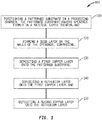
- Figure 1 is a flow diagram setting forth a method of forming a ruthenium doped copper seed layer, according to one embodiment.
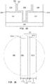
- Figures 2A-2E illustrate elements of the method set forth in Figure 1 .
- the method 100 includes positioning a patterned substrate in a processing chamber.
- a patterned substrate 200 is illustrated in Figure 2A and it includes a substrate 201, a material layer 209 formed on the substrate 201, one or more openings 205 formed in the material layer 209, and a barrier layer 206 disposed on, and lining the openings 205 of, the material layer 209.
- the material layer 209 comprises one or more dielectric layers, such as a first dielectric layer 202 and a second dielectric layer 204.
- the one or more dielectric layers 202, 204 are formed of a material selected from the group consisting of silicon oxides, SiN, SiOC, SIC, low-k polymers, such as a polyamide, and combinations thereof.
- the material layer 209 further comprises an etch stop layer 203 disposed between the first dielectric layer 202 and the second dielectric layer 204.
- the barrier layer 206 disposed on the material layer 209, prevents diffusion of copper atoms from subsequently deposited copper layers into the surrounding dielectric layers 202, 204.
- the barrier layer 206 comprises one or more of a metal, a metal nitride, a metal alloy, or a combination thereof.
- the barrier layer 206 is selected from the group consisting of tantalum, tantalum nitride, tungsten, titanium, titanium tungsten, titanium nitride, tungsten nitride, titanium copper, and combinations thereof.
- the barrier layer comprises tantalum nitride.
- the barrier layer 206 is deposited using any suitable method such as chemical vapor deposition (CVD), physical vapor deposition (PVD), atomic layer deposition (ALD), or combinations thereof.
- the method 100 includes forming a seed layer 207 on the barrier layer 206.
- Figure 2B illustrates a seed layer 207 deposited on the barrier layer 206 of the patterned substrate 200.
- Figure 2E is a close up view of a portion of Figure 2B .
- the method 100 includes depositing a first copper layer 207a on the barrier layer 206 of the patterned substrate 200.
- the first copper layer 207a herein is deposited using an atomic layer deposition (ALD) process which includes sequentially exposing the patterned substrate 200 to a first reactive precursor comprising a copper-containing organometallic and a then second reactive precursor comprising a hydrogen containing gas to form a copper film.
- ALD atomic layer deposition
- copper-containing organometallic gases include bis(diethylamino-2-n-butoxy)copper (Cu(DEAB)2), bis(ethylmethylamino-2-n-butoxy)copper, bis(dimethylamino-2-propoxy)copper (Cu(DMAP)2), bis(dimethylamino-2-n-butoxy)copper (Cu(DMAB)2), bis(dimethylamino-2-ethoxy)copper, bis(ethymethylamino-2-propoxy)copper (Cu(EMAP)2), bis(diethylamino-2-ethoxy)copper, bis(ethylmethylamino-2methyl-2-n-butoxy)copper, bis(dimethylamino-2-methyl-2-propoxy)copper, bis(diethylamino-2-propoxy) copper (Cu(DEAP)2), bis(2-methoxyethoxy)copper, bis(2,2,6,6-tetramethyl-3,5-hept
- the processing chamber is maintained at a pressure of between about 1 Torr and about 30 Torr and the patterned substrate is maintained a temperature between about 50 °C and about 400 °C during the deposition of the first copper layer 207a.
- Flowrates for the first and second reactive precursor are typically between about 3000 sccm and about 9000 sccm for a processing chamber configured to process 300 mm diameter substrates and are scaled appropriately for different sized substrates.
- the processing chamber is a plasma enhanced processing chamber where an electrode disposed in the processing chamber is coupled to a plasma power supply.
- the plasma power supply provides between about 100 W and 1000 W, such as about 400 W at a frequency of 13.56 MHz, to ignite and maintain the precursors into a processing plasma.
- the first copper layer 207a has a copper purity of greater than about 99%.
- the first copper layer is deposited using a physical vapor deposition (PVD) or a chemical vapor deposition (CVD) process.
- PVD physical vapor deposition
- CVD chemical vapor deposition
- the first copper layer 207a is deposited using a PVD process where the target is a pure copper target or a copper alloy target, such as a Cu-AI target comprising between about 0.1% and about 3% Al or a Cu-Mn target comprising between about 0.1% and about 3% Mn.
- the target is coupled to a DC power of between about 20 kW and about 40 kW and the substrate is coupled to an AC bias power of between about 50 W and about 1500 W.
- the first copper layer 207a is deposited using a CVD or PVD process.
- the method 100 includes depositing a ruthenium layer 207b onto the first copper layer 207a.
- the ruthenium layer 207b is deposited in the same processing chamber used to deposit the first copper layer 207a.
- the processing chamber is purged between depositing the first copper layer 207a and depositing the ruthenium layer, using an inert gas such as argon.
- the ruthenium layer 207b is deposited using an ALD process which includes alternating sequentially exposing the patterned substrate 200, having the first copper layer 207a deposited thereon, to a third reactive precursor comprising a ruthenium-containing organometallic and then a fourth reactive precursor comprising hydrogen, such as hydrogen gas.
- ruthenium-containing organometallics examples include methyl-cyclohexadine ruthenium tricarbonylcyclohexadine, ruthenium tricarbonyl, butadiene ruthenium tricarbonyl, dimethyl butadiene ruthenium tricarbonyl, modified dines with Ru(CO)3, and combinations thereof.
- the processing chamber is maintained at a pressure between about 1 Torr and about 50 Torr and the patterned substrate is maintained a temperature between about 100 °C and about 400 °C.
- Flowrates for the third and fourth reactive precursors are between about 3000 sccm and about 9000 sccm for an ALD processing chamber configured to process 300 mm diameter substrates and are scaled appropriately for different sized substrates.
- an electrode disposed in the processing chamber is coupled to a plasma power supply that provides between about 100 W and 1000 W, such as about 400 W at a frequency of 13.56 MHz which ignites and maintains a processing plasma of the precursor gases disposed therein.
- the processing volume is purged between alternating exposures of the third and fourth precursors using an inert gas, such as argon.
- an inert gas such as argon.
- the ruthenium layer 207b is deposited using a CVD process and/or is deposited in a different processing chamber than that used to form the first copper layer 207a.
- the ruthenium layer 207b is deposited using a PVD process.
- the method 100 includes depositing a second copper layer 207c on the ruthenium layer 207b.
- the second copper layer 207c is deposited in the same processing chamber as was used to form the first copper layer 207a at activity 130 and the ruthenium layer 207b at activity 140.
- the second copper layer 207c is deposited using the same process used to from the first copper layer 207a at activity 130.
- the ALD processing chamber is purged with an inert gas, such as argon, between depositing the ruthenium layer 207b and the second copper layer 207c.
- the second copper layer 207c is deposited using a PVD process or a CVD process in a chamber that is different from the chamber used to form the first copper layer 207a and/or the ruthenium layer 207b.
- the processing chambers used to form the barrier layer 206, the copper layers 207a, 207c, and/or the ruthenium layer 207b are connected together under vacuum or a controlled environment by a transfer chamber which is maintained at sub-atmospheric pressures to prevent surface oxidation of the deposited layers before formation of a subsequent layer thereon.
- the barrier layer 206 has a first thickness T(1) between about 0.5 nm and about 20 nm, such as between about 1 nm and about 5 nm, for example about 2 nm.
- the first copper layer 207a has a second thickness T(2) between about 0.5 nm and about 20 nm, such as between about 0.5 nm and about 10 nm, such as between about 0.5 nm and about 5 nm, for example about 4 nm.
- the ruthenium layer 207b has a third thickness T(3) between about 1 angstrom ( ⁇ ) and about 20 ⁇ , such as between about 1 ⁇ and about 15 ⁇ , such as between about 1 ⁇ and about 10 ⁇ .
- the second copper layer 207c has a fourth thickness T(4) between about 0.5 nm and about 200 nm, such as between about 1 nm and about 20 nm, or between about 1 nm and about 5 nm, for example about 2 nm.
- the ratio of copper to ruthenium in the seed layer 207 is between about 99.9:1 and about 4:1, where the thicknesses T(2), T(3), and T(4) of the respective copper and ruthenium layers 207a, 207b, and 207c is adjusted to increase or decrease the concentration of ruthenium in the seed layer.
- forming the seed layer 207 comprises sequentially depositing a plurality of first copper layers 207a and ruthenium layers 207b before depositing the second and final copper layer 207c.
- Figures 2D and 2E further illustrate the formation of a copper interconnect.
- Figure 2D shows a bulk copper layer 208 deposited on the seed layer using an electroplating process or a copper reflow / gap fill process, e.g., a thermal assisted reflow process.
- the bulk copper layer 208 is then removed from the surface of the substrate using a bulk film removal process, such as chemical mechanical planarization (CMP), to form a copper interconnect structure, such as the interconnect structure shown in Figure 2D .
- CMP chemical mechanical planarization
- Benefits of the methods described herein include suppressed copper agglomeration during formation of the seed layer, reduction in the minimum seed layer thickness required for continuous coverage thereof, improved reflow fill with thinner seed layer, and improved line and/or via resistance of a copper interconnect formed thereon. Further, in addition to suppressed copper agglomeration, benefits of embodiments herein include suppressed copper electromigration which allows for increased circuit density and improved reliability and/or useful lifetime by preventing device failures related thereto.
Landscapes
- Internal Circuitry In Semiconductor Integrated Circuit Devices (AREA)
- Electrodes Of Semiconductors (AREA)
- Electroplating Methods And Accessories (AREA)
Abstract
Description
- Embodiments described herein generally relate to the field of semiconductor device manufacturing, and more particularly, to methods of forming seed layers for copper interconnects.
- As circuit densities increase for next generation devices and transistor dimensions continue to shrink, the resistance and conductivity of wire interconnects begins to dominate device performance for major device performance metrics including power consumption, resistance-capacitance (RC) delay, and reliability. Copper is one material used for wire interconnects in advanced USLI and VSLI technologies, because copper generally exhibits relatively low resistivity and high conductivity. Often, copper interconnects are formed by depositing a copper seed layer into openings formed in a material surface of a substrate before electroplating bulk copper onto the copper seed layer or before bulk copper reflow thereinto.
- Typically, the copper seed layer carries the required electrical current for a subsequent electroplating process or serves as a wetting layer to promote copper reflow into the openings formed in the material surface of the substrate. Gaps in coverage of the copper seed layer on the walls or base of the openings will lead to undesirable voids in the bulk copper material of the interconnect structure. Voids or coverage gaps in the bulk copper material result in electro-migration failures of copper structures, which potentially render the resulting device useless or having lessened capability. Causes of copper seed layer coverage gaps include one or both of copper agglomeration or discontinuous deposition. Copper agglomeration occurs when the deposited copper coalesces into thicker coverage in some areas by pulling copper away from surrounding areas. Discontinuous deposition on the walls of the openings is typically due to a shadowing effect inherent to the copper seed physical vapor deposition (PVD) process for some opening geometries.
- Conductive liners deposited on the copper seed layer, such as a metal liner, fill gaps in coverage of the seed layer on the walls or base of the openings which reduces voids in the bulk copper material during the subsequent electroplating process. However, conductive liners disposed between the copper seed layer and the bulk copper layer undesirably create an interfacial liner/copper layer between the copper seed layer and bulk copper layer. This interfacial layer undesirably reduces the total copper line width and thus undesirably increases the line resistivity of the subsequently formed copper interconnect.
- Accordingly, what is need in the art improved copper seed layers and methods of forming improved copper seed layers.
- The present disclosure generally describes methods of forming a ruthenium doped copper seed layer.
- In one embodiment, a method of forming an interconnect structure is provided. The method comprises positioning a patterned substrate in a first processing chamber, the patterned substrate having openings formed in a material layer thereof, and forming a seed layer on walls of the openings. Forming the seed layer on the walls of the openings includes forming first copper layer, forming a ruthenium layer on the first copper layer, and forming a second copper layer on the ruthenium layer.
- In another embodiment, a method of forming a device includes depositing a first copper layer on a patterned substrate, the patterned substrate comprising a material layer having openings formed therein and a barrier layer disposed on the material layer, depositing a ruthenium layer on the first copper layer, and depositing a second copper layer on the ruthenium layer. In some embodiments, the method further includes depositing a copper layer into the opening using an electrodeposition process, a reflow gap fill process, or a combination thereof.
- In another embodiment, a method of forming a copper interconnect includes positioning a patterned substrate in a processing chamber, the patterned substrate having openings formed in a material layer thereof, and forming a seed layer on walls of the openings. Forming the seed layer on the walls of the openings comprises depositing a first copper layer on the patterned substrate, depositing a ruthenium layer on the first copper layer, and depositing a second copper layer on the ruthenium layer. Depositing the first copper layer comprises sequentially exposing the patterned substrate to a first reactive precursor comprising a copper-containing organometallic and a second reactive precursor comprising hydrogen. Depositing the ruthenium layer incudes sequentially exposing the first copper layer to a third reactive precursor comprising a ruthenium-containing organometallic and a fourth reactive precursor comprising hydrogen. Depositing the second copper layer comprises sequentially exposing the ruthenium layer to the first reactive precursor and the second reactive precursor.
- In some embodiments, the methods described herein further include depositing a copper layer into the opening using an electrodeposition process, a reflow gap fill process, or a combination thereof.
- In another embodiment, a device, comprises a substrate featuring a patterned surface, the pattern surface having a plurality of openings formed in a material layer thereof, and a seed layer disposed on walls of the openings. Here, the seed layer includes a first copper layer, a ruthenium layer disposed on the first copper layer, and a second copper layer disposed on the ruthenium layer.
- So that the manner in which the above recited features of the present disclosure can be understood in detail, a more particular description of the disclosure, briefly summarized above, may be had by reference to embodiments, some of which are illustrated in the appended drawings. It is to be noted, however, that the appended drawings illustrate only typical embodiments of this disclosure and are therefore not to be considered limiting of its scope, for the disclosure may admit to other equally effective embodiments.
-
Figure 1 is a flow diagram setting forth a method of forming a ruthenium doped copper seed layer, according to one embodiment. -
Figures 2A-2E illustrate element of the method set forth inFigure 1 , according to one embodiment - To facilitate understanding, identical reference numerals have been used, where possible, to designate identical elements that are common to the figures. It is contemplated that elements and features of one embodiment may be beneficially incorporated in other embodiments without further recitation.
- Embodiments of the present disclosure generally describe methods of forming a copper interconnect structure, in particular, forming a ruthenium doped copper seed layer comprising a plurality of copper layers and at least one ruthenium layer disposed between the copper layers. The methods described herein may be performed in a physical vapor deposition (PVD) processing chamber, a chemical vapor deposition (CVD) processing chamber, an atomic layer deposition (ALD) processing chamber, or combinations thereof. In one embodiment, the PVD, CVD, and ALD processing chambers are an ENDURA® PVD processing chamber, a PRODUCER® CVD processing chamber, and an OLYMPIA® ALD processing chamber respectively, all available from Applied Materials, Inc., Santa Clara, California.
- A ruthenium doped seed layer, formed according to the methods described herein, enables continuous seed layer coverage over the walls of interconnect openings and facilitates reducing liner thicknesses Herein, the ruthenium doped seed layer includes at least one ruthenium layer deposited between a first copper layer and a second copper layer. Typically, the first and second copper layers are deposited using a PVD process, a CVD process, or an ALD process and the ruthenium layer is deposited using a CVD process or an ALD process. Copper and ruthenium are generally not miscible with one another, thus the ruthenium layer effectively pins the copper of either the first and second layers at the grain boundaries formed therebetween and desirably locks the copper in place in the feature preventing electromigration thereof. Pinning the copper at the grain boundaries formed between the copper and ruthenium layers prevents the copper in the copper layers from moving to form undesirable copper agglomerations. Further, preventing copper electromigration using the methods set forth herein allows for increased circuit density and improved reliability by preventing device failures related thereto.
- Benefits of suppressing copper agglomeration using embodiments provided herein further include enabling a reduction in the thickness of a liner layer disposed on a dielectric layer having the opening formed therein. The reduced thickness of the liner layer increases the bulk copper volume for the subsequently formed interconnect. This increase in bulk copper volume desirably reduces line resistance in the opening. Pinning the copper layer desirably eliminates gaps in coverage on the walls of interconnect feature openings. Eliminating coverage gaps caused by copper migration desirably eliminates or reduces voids formed in the bulk copper material of the copper interconnect during a subsequent electrodeposition or reflow / gap fill process. Beneficially, ruthenium diffuses more slowly into copper than other dopants, such as cobalt or manganese, so that by using ruthenium in the seed layer, the line resistance of the bulk copper layer is not negatively impacted. Further, the ruthenium doped seed layers formed according to embodiments described provide a relativity thin and continuous surface to facilitate a subsequent copper reflow / gap fill process.
-
Figure 1 is a flow diagram setting forth a method of forming a ruthenium doped copper seed layer, according to one embodiment.Figures 2A-2E illustrate elements of the method set forth inFigure 1 . - At
activity 110 themethod 100 includes positioning a patterned substrate in a processing chamber. A patternedsubstrate 200 is illustrated inFigure 2A and it includes asubstrate 201, amaterial layer 209 formed on thesubstrate 201, one ormore openings 205 formed in thematerial layer 209, and abarrier layer 206 disposed on, and lining theopenings 205 of, thematerial layer 209. Herein, thematerial layer 209 comprises one or more dielectric layers, such as a firstdielectric layer 202 and a seconddielectric layer 204. Typically, the one or moredielectric layers - In some embodiments, the
material layer 209 further comprises anetch stop layer 203 disposed between the firstdielectric layer 202 and the seconddielectric layer 204. Thebarrier layer 206, disposed on thematerial layer 209, prevents diffusion of copper atoms from subsequently deposited copper layers into the surroundingdielectric layers barrier layer 206 comprises one or more of a metal, a metal nitride, a metal alloy, or a combination thereof. In some embodiments, thebarrier layer 206 is selected from the group consisting of tantalum, tantalum nitride, tungsten, titanium, titanium tungsten, titanium nitride, tungsten nitride, titanium copper, and combinations thereof. In some embodiments, the barrier layer comprises tantalum nitride. Thebarrier layer 206 is deposited using any suitable method such as chemical vapor deposition (CVD), physical vapor deposition (PVD), atomic layer deposition (ALD), or combinations thereof. - At
activity 120 themethod 100 includes forming aseed layer 207 on thebarrier layer 206.Figure 2B illustrates aseed layer 207 deposited on thebarrier layer 206 of the patternedsubstrate 200.Figure 2E is a close up view of a portion ofFigure 2B . - At
activity 130 themethod 100 includes depositing afirst copper layer 207a on thebarrier layer 206 of the patternedsubstrate 200. Thefirst copper layer 207a herein is deposited using an atomic layer deposition (ALD) process which includes sequentially exposing the patternedsubstrate 200 to a first reactive precursor comprising a copper-containing organometallic and a then second reactive precursor comprising a hydrogen containing gas to form a copper film. Examples of copper-containing organometallic gases include bis(diethylamino-2-n-butoxy)copper (Cu(DEAB)2), bis(ethylmethylamino-2-n-butoxy)copper, bis(dimethylamino-2-propoxy)copper (Cu(DMAP)2), bis(dimethylamino-2-n-butoxy)copper (Cu(DMAB)2), bis(dimethylamino-2-ethoxy)copper, bis(ethymethylamino-2-propoxy)copper (Cu(EMAP)2), bis(diethylamino-2-ethoxy)copper, bis(ethylmethylamino-2methyl-2-n-butoxy)copper, bis(dimethylamino-2-methyl-2-propoxy)copper, bis(diethylamino-2-propoxy) copper (Cu(DEAP)2), bis(2-methoxyethoxy)copper, bis(2,2,6,6-tetramethyl-3,5-heptanedionate) copper, bis(2,2,6,6-tetramethyl-3,5-heptaneketoiminate) copper, bis(2-methoxy-2-propoxy)copper, and 2,2,6,6-tetramethyl-3,5-heptanedionate copper (TMVS), and combinations thereof. Examples of the hydrogen containing precursor include H2, NH3, and combinations thereof. In some embodiments, the processing volume is purged between alternating exposures of the first and second precursors using an inert gas, such as argon. - In some embodiments, the processing chamber is maintained at a pressure of between about 1 Torr and about 30 Torr and the patterned substrate is maintained a temperature between about 50 °C and about 400 °C during the deposition of the
first copper layer 207a. Flowrates for the first and second reactive precursor are typically between about 3000 sccm and about 9000 sccm for a processing chamber configured to process 300 mm diameter substrates and are scaled appropriately for different sized substrates. In some embodiments, the processing chamber is a plasma enhanced processing chamber where an electrode disposed in the processing chamber is coupled to a plasma power supply. The plasma power supply provides between about 100 W and 1000 W, such as about 400 W at a frequency of 13.56 MHz, to ignite and maintain the precursors into a processing plasma. In some embodiments, thefirst copper layer 207a has a copper purity of greater than about 99%. In other embodiments, the first copper layer is deposited using a physical vapor deposition (PVD) or a chemical vapor deposition (CVD) process. For example, in one embodiment thefirst copper layer 207a is deposited using a PVD process where the target is a pure copper target or a copper alloy target, such as a Cu-AI target comprising between about 0.1% and about 3% Al or a Cu-Mn target comprising between about 0.1% and about 3% Mn. In that embodiment, the target is coupled to a DC power of between about 20 kW and about 40 kW and the substrate is coupled to an AC bias power of between about 50 W and about 1500 W. In another embodiment, thefirst copper layer 207a is deposited using a CVD or PVD process. - At
activity 140 themethod 100 includes depositing aruthenium layer 207b onto thefirst copper layer 207a. Here, theruthenium layer 207b is deposited in the same processing chamber used to deposit thefirst copper layer 207a. Typically, the processing chamber is purged between depositing thefirst copper layer 207a and depositing the ruthenium layer, using an inert gas such as argon. In some embodiments, theruthenium layer 207b is deposited using an ALD process which includes alternating sequentially exposing the patternedsubstrate 200, having thefirst copper layer 207a deposited thereon, to a third reactive precursor comprising a ruthenium-containing organometallic and then a fourth reactive precursor comprising hydrogen, such as hydrogen gas. Examples of ruthenium-containing organometallics include methyl-cyclohexadine ruthenium tricarbonylcyclohexadine, ruthenium tricarbonyl, butadiene ruthenium tricarbonyl, dimethyl butadiene ruthenium tricarbonyl, modified dines with Ru(CO)3, and combinations thereof. - Typically, during deposition of the
ruthenium layer 207b, the processing chamber is maintained at a pressure between about 1 Torr and about 50 Torr and the patterned substrate is maintained a temperature between about 100 °C and about 400 °C. Flowrates for the third and fourth reactive precursors are between about 3000 sccm and about 9000 sccm for an ALD processing chamber configured to process 300 mm diameter substrates and are scaled appropriately for different sized substrates. In some embodiments, an electrode disposed in the processing chamber is coupled to a plasma power supply that provides between about 100 W and 1000 W, such as about 400 W at a frequency of 13.56 MHz which ignites and maintains a processing plasma of the precursor gases disposed therein. In some embodiments, the processing volume is purged between alternating exposures of the third and fourth precursors using an inert gas, such as argon. In other embodiments, theruthenium layer 207b is deposited using a CVD process and/or is deposited in a different processing chamber than that used to form thefirst copper layer 207a. In other embodiments, theruthenium layer 207b is deposited using a PVD process. - At
activity 150 themethod 100 includes depositing asecond copper layer 207c on theruthenium layer 207b. In some embodiments, thesecond copper layer 207c is deposited in the same processing chamber as was used to form thefirst copper layer 207a atactivity 130 and theruthenium layer 207b atactivity 140. In some embodiments, thesecond copper layer 207c is deposited using the same process used to from thefirst copper layer 207a atactivity 130. Typically, the ALD processing chamber is purged with an inert gas, such as argon, between depositing theruthenium layer 207b and thesecond copper layer 207c. In other embodiments, thesecond copper layer 207c is deposited using a PVD process or a CVD process in a chamber that is different from the chamber used to form thefirst copper layer 207a and/or theruthenium layer 207b. In some embodiments, the processing chambers used to form thebarrier layer 206, thecopper layers ruthenium layer 207b are connected together under vacuum or a controlled environment by a transfer chamber which is maintained at sub-atmospheric pressures to prevent surface oxidation of the deposited layers before formation of a subsequent layer thereon. - Herein, the
barrier layer 206 has a first thickness T(1) between about 0.5 nm and about 20 nm, such as between about 1 nm and about 5 nm, for example about 2 nm. Thefirst copper layer 207a has a second thickness T(2) between about 0.5 nm and about 20 nm, such as between about 0.5 nm and about 10 nm, such as between about 0.5 nm and about 5 nm, for example about 4 nm. Theruthenium layer 207b has a third thickness T(3) between about 1 angstrom (Å) and about 20 Å, such as between about 1 Å and about 15 Å, such as between about 1 Å and about 10 Å. Thesecond copper layer 207c has a fourth thickness T(4) between about 0.5 nm and about 200 nm, such as between about 1 nm and about 20 nm, or between about 1 nm and about 5 nm, for example about 2 nm. Typically, the ratio of copper to ruthenium in theseed layer 207 is between about 99.9:1 and about 4:1, where the thicknesses T(2), T(3), and T(4) of the respective copper andruthenium layers - In some embodiments, forming the
seed layer 207 comprises sequentially depositing a plurality offirst copper layers 207a andruthenium layers 207b before depositing the second andfinal copper layer 207c. -
Figures 2D and 2E further illustrate the formation of a copper interconnect.Figure 2D shows abulk copper layer 208 deposited on the seed layer using an electroplating process or a copper reflow / gap fill process, e.g., a thermal assisted reflow process. Thebulk copper layer 208 is then removed from the surface of the substrate using a bulk film removal process, such as chemical mechanical planarization (CMP), to form a copper interconnect structure, such as the interconnect structure shown inFigure 2D . - Benefits of the methods described herein include suppressed copper agglomeration during formation of the seed layer, reduction in the minimum seed layer thickness required for continuous coverage thereof, improved reflow fill with thinner seed layer, and improved line and/or via resistance of a copper interconnect formed thereon. Further, in addition to suppressed copper agglomeration, benefits of embodiments herein include suppressed copper electromigration which allows for increased circuit density and improved reliability and/or useful lifetime by preventing device failures related thereto.
- While the foregoing is directed to embodiments of the present disclosure, other and further embodiments of the disclosure may be devised without departing from the basic scope thereof, and the scope thereof is determined by the claims that follow.
Claims (15)
- A method of forming an interconnect structure, comprising:positioning a substrate in a first processing chamber, the substrate comprising a patterned surface having openings formed in a material layer thereof; andforming a seed layer on walls of the openings, comprising:forming a first copper layer on the walls of the openings;forming a ruthenium layer on the first copper layer; andforming a second copper layer on the ruthenium layer.
- The method of claim 1, wherein forming the ruthenium layer comprises sequential repetitions of exposing the substrate to a ruthenium precursor and exposing the substrate to a hydrogen-containing precursor.
- The method of claim 1, wherein the ruthenium layer is formed in a second processing chamber that is different from the first processing chamber used to form the first copper layer.
- The method of claim 1, wherein the first copper layer, the ruthenium layer, and the second copper layer are formed in the first processing chamber without removing the substrate therefrom.
- The method of claim 1, wherein a thickness of the ruthenium layer is between about 1 angstrom and about 20 angstroms.
- The method of claim 1, wherein the patterned surface further comprises a barrier layer disposed on the material layer, the barrier layer comprising a material selected from the group consisting of tantalum, tantalum nitride, tungsten, titanium, titanium tungsten, titanium nitride, tungsten nitride, titanium copper, and combinations thereof, and wherein the first copper layer is formed on the barrier layer.
- The method of claim 6, wherein the barrier layer is deposited in a second processing chamber, and wherein the first processing chamber and the second processing chamber are connected together by a transfer chamber.
- The method of claim 1, wherein forming the first copper layer comprises sequential repetitions of exposing the substrate to a copper precursor and exposing the substrate to a hydrogen precursor.
- A method of forming a device, comprising:depositing a first copper layer on a patterned substrate, the patterned substrate comprising a material layer having openings formed therein and a barrier layer disposed on the material layer;depositing a ruthenium layer on the first copper layer; anddepositing a second copper layer on the ruthenium layer.
- The method of claim 9, wherein the material layer comprises a dielectric layer.
- The method of claim 10, wherein the barrier layer comprises a material selected from the group consisting of tantalum, tantalum nitride, tungsten, titanium, titanium tungsten, titanium nitride, tungsten nitride, titanium copper, and combinations thereof.
- The method of claim 11, wherein depositing the first and second copper layers comprises sequentially exposing the patterned substrate to a first reactive precursor comprising a copper-containing organometallic and a second reactive precursor comprising hydrogen.
- A device, comprising:a substrate comprising a patterned surface having a plurality of openings formed in a material layer thereof; anda seed layer disposed on walls of the openings, the seed layer comprising:a first copper layer;a ruthenium layer disposed on the first copper layer; anda second copper layer disposed on the ruthenium layer.
- The device of claim 13, wherein a thickness of the ruthenium layer is between about 1 angstrom and about 20 angstroms.
- The device of claim 13, wherein the material layer comprises a dielectric material and the device further comprises a barrier layer interposed between the seed layer and the walls of the openings, and wherein the barrier layer comprises a material selected from the group consisting of tantalum, tantalum nitride, tungsten, titanium, titanium tungsten, titanium nitride, tungsten nitride, titanium copper, and combinations thereof.
Applications Claiming Priority (1)
| Application Number | Priority Date | Filing Date | Title |
|---|---|---|---|
| US201762548604P | 2017-08-22 | 2017-08-22 |
Publications (2)
| Publication Number | Publication Date |
|---|---|
| EP3447793A1 true EP3447793A1 (en) | 2019-02-27 |
| EP3447793B1 EP3447793B1 (en) | 2021-01-06 |
Family
ID=63350353
Family Applications (1)
| Application Number | Title | Priority Date | Filing Date |
|---|---|---|---|
| EP18189568.1A Not-in-force EP3447793B1 (en) | 2017-08-22 | 2018-08-17 | Method for producing seed layers for copper interconnects |
Country Status (6)
| Country | Link |
|---|---|
| US (1) | US10847463B2 (en) |
| EP (1) | EP3447793B1 (en) |
| JP (2) | JP7634930B2 (en) |
| KR (1) | KR20190021184A (en) |
| CN (1) | CN109461698B (en) |
| TW (1) | TWI803510B (en) |
Families Citing this family (5)
| Publication number | Priority date | Publication date | Assignee | Title |
|---|---|---|---|---|
| US11177162B2 (en) * | 2019-09-17 | 2021-11-16 | International Business Machines Corporation | Trapezoidal interconnect at tight BEOL pitch |
| CN114664656A (en) * | 2020-05-22 | 2022-06-24 | 北京屹唐半导体科技股份有限公司 | Workpiece processing using ozone gas and hydrogen radicals |
| US11410881B2 (en) | 2020-06-28 | 2022-08-09 | Applied Materials, Inc. | Impurity removal in doped ALD tantalum nitride |
| US11764157B2 (en) * | 2020-07-23 | 2023-09-19 | Applied Materials, Inc. | Ruthenium liner and cap for back-end-of-line applications |
| WO2025005521A1 (en) * | 2023-06-30 | 2025-01-02 | 주성엔지니어링(주) | Method for forming electrode |
Citations (6)
| Publication number | Priority date | Publication date | Assignee | Title |
|---|---|---|---|---|
| US20060199372A1 (en) * | 2005-03-01 | 2006-09-07 | Applied Materials, Inc. | Reduction of copper dewetting by transition metal deposition |
| US20090087982A1 (en) * | 2007-09-28 | 2009-04-02 | Applied Materials, Inc. | Selective ruthenium deposition on copper materials |
| WO2009146423A1 (en) * | 2008-05-30 | 2009-12-03 | Sigma-Aldrich Co. | Methods of forming ruthenium-containing films by atomic layer deposition |
| US20140327141A1 (en) * | 2012-04-13 | 2014-11-06 | Taiwan Semiconductor Manufacturing Company, Ltd. | Copper interconnect structure and method for forming the same |
| US20150262938A1 (en) * | 2014-03-14 | 2015-09-17 | Taiwan Semiconductor Manufacturing Company, Ltd. | Barrier Structure for Copper Interconnect |
| US20160032455A1 (en) * | 2014-07-31 | 2016-02-04 | Applied Materials, Inc. | High through-put and low temperature ald copper deposition and integration |
Family Cites Families (25)
| Publication number | Priority date | Publication date | Assignee | Title |
|---|---|---|---|---|
| US7910165B2 (en) * | 2002-06-04 | 2011-03-22 | Applied Materials, Inc. | Ruthenium layer formation for copper film deposition |
| US7101790B2 (en) | 2003-03-28 | 2006-09-05 | Taiwan Semiconductor Manufacturing Co., Ltd. | Method of forming a robust copper interconnect by dilute metal doping |
| JP2006097044A (en) * | 2004-09-28 | 2006-04-13 | L'air Liquide Sa Pour L'etude & L'exploitation Des Procede S Georges Claude | Film forming precursor, ruthenium-containing film forming method, ruthenium film forming method, ruthenium oxide film forming method, and ruthenate film forming method |
| US20060246699A1 (en) * | 2005-03-18 | 2006-11-02 | Weidman Timothy W | Process for electroless copper deposition on a ruthenium seed |
| JP2008098449A (en) * | 2006-10-12 | 2008-04-24 | Ebara Corp | Substrate processing apparatus and substrate processing method |
| US20080164613A1 (en) | 2007-01-10 | 2008-07-10 | International Business Machines Corporation | ULTRA-THIN Cu ALLOY SEED FOR INTERCONNECT APPLICATION |
| US20080223287A1 (en) * | 2007-03-15 | 2008-09-18 | Lavoie Adrien R | Plasma enhanced ALD process for copper alloy seed layers |
| US20100200991A1 (en) * | 2007-03-15 | 2010-08-12 | Rohan Akolkar | Dopant Enhanced Interconnect |
| US7659204B2 (en) * | 2007-03-26 | 2010-02-09 | Applied Materials, Inc. | Oxidized barrier layer |
| JP2009116952A (en) * | 2007-11-06 | 2009-05-28 | Hitachi Global Storage Technologies Netherlands Bv | Perpendicular magnetic recording medium and magnetic storage device using the same |
| US7964497B2 (en) * | 2008-06-27 | 2011-06-21 | International Business Machines Corporation | Structure to facilitate plating into high aspect ratio vias |
| US20090321935A1 (en) | 2008-06-30 | 2009-12-31 | O'brien Kevin | Methods of forming improved electromigration resistant copper films and structures formed thereby |
| US8084104B2 (en) | 2008-08-29 | 2011-12-27 | Asm Japan K.K. | Atomic composition controlled ruthenium alloy film formed by plasma-enhanced atomic layer deposition |
| JP2010215982A (en) * | 2009-03-18 | 2010-09-30 | Tosoh Corp | Method for producing ruthenium-containing film using ruthenium complex organic solvent solution, and ruthenium-containing film |
| JP2012074608A (en) * | 2010-09-29 | 2012-04-12 | Tokyo Electron Ltd | Wiring formation method |
| CN102332426A (en) * | 2011-09-23 | 2012-01-25 | 复旦大学 | Manufacturing method of copper diffusion impervious layers for nanometer ICs (integrated circuits) |
| US9076661B2 (en) * | 2012-04-13 | 2015-07-07 | Applied Materials, Inc. | Methods for manganese nitride integration |
| CN102903699A (en) * | 2012-10-15 | 2013-01-30 | 复旦大学 | Copper interconnecting structure and preparation method thereof |
| US20140134351A1 (en) * | 2012-11-09 | 2014-05-15 | Applied Materials, Inc. | Method to deposit cvd ruthenium |
| CN103266304B (en) | 2013-05-31 | 2015-12-23 | 江苏科技大学 | A kind of preparation method of Cu(Ru) alloy material without diffusion barrier layer with high thermal stability |
| JP6278827B2 (en) * | 2014-05-14 | 2018-02-14 | 株式会社Adeka | Copper compound, raw material for thin film formation, and method for producing thin film |
| US9768060B2 (en) * | 2014-10-29 | 2017-09-19 | Applied Materials, Inc. | Systems and methods for electrochemical deposition on a workpiece including removing contamination from seed layer surface prior to ECD |
| US10002834B2 (en) * | 2015-03-11 | 2018-06-19 | Applied Materials, Inc. | Method and apparatus for protecting metal interconnect from halogen based precursors |
| KR20160123793A (en) * | 2015-04-17 | 2016-10-26 | 포항공과대학교 산학협력단 | Resistive switching memory with double layered structure and method of fabricating the same |
| CN105355620B (en) * | 2015-12-17 | 2018-06-22 | 上海集成电路研发中心有限公司 | A kind of copper interconnection structure and its manufacturing method |
-
2018
- 2018-08-13 US US16/102,533 patent/US10847463B2/en active Active
- 2018-08-17 EP EP18189568.1A patent/EP3447793B1/en not_active Not-in-force
- 2018-08-21 JP JP2018154364A patent/JP7634930B2/en active Active
- 2018-08-22 KR KR1020180097909A patent/KR20190021184A/en not_active Ceased
- 2018-08-22 TW TW107129279A patent/TWI803510B/en active
- 2018-08-22 CN CN201810960756.9A patent/CN109461698B/en active Active
-
2023
- 2023-09-25 JP JP2023159999A patent/JP2023182638A/en active Pending
Patent Citations (6)
| Publication number | Priority date | Publication date | Assignee | Title |
|---|---|---|---|---|
| US20060199372A1 (en) * | 2005-03-01 | 2006-09-07 | Applied Materials, Inc. | Reduction of copper dewetting by transition metal deposition |
| US20090087982A1 (en) * | 2007-09-28 | 2009-04-02 | Applied Materials, Inc. | Selective ruthenium deposition on copper materials |
| WO2009146423A1 (en) * | 2008-05-30 | 2009-12-03 | Sigma-Aldrich Co. | Methods of forming ruthenium-containing films by atomic layer deposition |
| US20140327141A1 (en) * | 2012-04-13 | 2014-11-06 | Taiwan Semiconductor Manufacturing Company, Ltd. | Copper interconnect structure and method for forming the same |
| US20150262938A1 (en) * | 2014-03-14 | 2015-09-17 | Taiwan Semiconductor Manufacturing Company, Ltd. | Barrier Structure for Copper Interconnect |
| US20160032455A1 (en) * | 2014-07-31 | 2016-02-04 | Applied Materials, Inc. | High through-put and low temperature ald copper deposition and integration |
Also Published As
| Publication number | Publication date |
|---|---|
| JP2019062190A (en) | 2019-04-18 |
| JP7634930B2 (en) | 2025-02-25 |
| US20190067201A1 (en) | 2019-02-28 |
| TWI803510B (en) | 2023-06-01 |
| JP2023182638A (en) | 2023-12-26 |
| EP3447793B1 (en) | 2021-01-06 |
| US10847463B2 (en) | 2020-11-24 |
| CN109461698B (en) | 2024-04-12 |
| TW201920735A (en) | 2019-06-01 |
| KR20190021184A (en) | 2019-03-05 |
| CN109461698A (en) | 2019-03-12 |
Similar Documents
| Publication | Publication Date | Title |
|---|---|---|
| KR102036245B1 (en) | Doped tantalum nitride for copper barrier applications | |
| KR102189781B1 (en) | Methods for depositing manganese and manganese nitrides | |
| US8617982B2 (en) | Subtractive patterning to define circuit components | |
| EP3447793B1 (en) | Method for producing seed layers for copper interconnects | |
| US9343402B2 (en) | Semiconductor device having Ti- and N-containing layer, and manufacturing method of same | |
| US8058164B2 (en) | Methods of fabricating electronic devices using direct copper plating | |
| KR20190050869A (en) | Doped optional metal cap to improve copper electron transfer with ruthenium liner | |
| WO1999009593A1 (en) | Dual damascene metallization | |
| US10373867B2 (en) | Cobalt contact and interconnect structures | |
| KR100443796B1 (en) | Method for forming a copper metal line | |
| KR100622639B1 (en) | Manufacturing Method of Semiconductor Device | |
| KR100667905B1 (en) | Copper metal wiring formation method of semiconductor device | |
| US20250233015A1 (en) | Methods of manufacturing interconnect structures | |
| KR20190081455A (en) | Method of manufacturing a cobalt-containing thin film | |
| KR20050029757A (en) | Semiconductor device and a method of manufacturing the same |
Legal Events
| Date | Code | Title | Description |
|---|---|---|---|
| PUAI | Public reference made under article 153(3) epc to a published international application that has entered the european phase |
Free format text: ORIGINAL CODE: 0009012 |
|
| STAA | Information on the status of an ep patent application or granted ep patent |
Free format text: STATUS: THE APPLICATION HAS BEEN PUBLISHED |
|
| AK | Designated contracting states |
Kind code of ref document: A1 Designated state(s): AL AT BE BG CH CY CZ DE DK EE ES FI FR GB GR HR HU IE IS IT LI LT LU LV MC MK MT NL NO PL PT RO RS SE SI SK SM TR |
|
| AX | Request for extension of the european patent |
Extension state: BA ME |
|
| STAA | Information on the status of an ep patent application or granted ep patent |
Free format text: STATUS: REQUEST FOR EXAMINATION WAS MADE |
|
| 17P | Request for examination filed |
Effective date: 20190820 |
|
| RBV | Designated contracting states (corrected) |
Designated state(s): AL AT BE BG CH CY CZ DE DK EE ES FI FR GB GR HR HU IE IS IT LI LT LU LV MC MK MT NL NO PL PT RO RS SE SI SK SM TR |
|
| REG | Reference to a national code |
Ref country code: DE Ref legal event code: R079 Ref document number: 602018011516 Country of ref document: DE Free format text: PREVIOUS MAIN CLASS: H01L0021768000 Ipc: H01L0021285000 |
|
| GRAP | Despatch of communication of intention to grant a patent |
Free format text: ORIGINAL CODE: EPIDOSNIGR1 |
|
| STAA | Information on the status of an ep patent application or granted ep patent |
Free format text: STATUS: GRANT OF PATENT IS INTENDED |
|
| RIC1 | Information provided on ipc code assigned before grant |
Ipc: H01L 21/768 20060101ALI20200708BHEP Ipc: H01L 21/285 20060101AFI20200708BHEP |
|
| INTG | Intention to grant announced |
Effective date: 20200727 |
|
| GRAS | Grant fee paid |
Free format text: ORIGINAL CODE: EPIDOSNIGR3 |
|
| GRAA | (expected) grant |
Free format text: ORIGINAL CODE: 0009210 |
|
| STAA | Information on the status of an ep patent application or granted ep patent |
Free format text: STATUS: THE PATENT HAS BEEN GRANTED |
|
| AK | Designated contracting states |
Kind code of ref document: B1 Designated state(s): AL AT BE BG CH CY CZ DE DK EE ES FI FR GB GR HR HU IE IS IT LI LT LU LV MC MK MT NL NO PL PT RO RS SE SI SK SM TR |
|
| REG | Reference to a national code |
Ref country code: GB Ref legal event code: FG4D |
|
| REG | Reference to a national code |
Ref country code: AT Ref legal event code: REF Ref document number: 1353274 Country of ref document: AT Kind code of ref document: T Effective date: 20210115 Ref country code: CH Ref legal event code: EP |
|
| REG | Reference to a national code |
Ref country code: DE Ref legal event code: R096 Ref document number: 602018011516 Country of ref document: DE |
|
| REG | Reference to a national code |
Ref country code: IE Ref legal event code: FG4D |
|
| REG | Reference to a national code |
Ref country code: NL Ref legal event code: MP Effective date: 20210106 |
|
| REG | Reference to a national code |
Ref country code: AT Ref legal event code: MK05 Ref document number: 1353274 Country of ref document: AT Kind code of ref document: T Effective date: 20210106 |
|
| REG | Reference to a national code |
Ref country code: LT Ref legal event code: MG9D |
|
| PG25 | Lapsed in a contracting state [announced via postgrant information from national office to epo] |
Ref country code: PT Free format text: LAPSE BECAUSE OF FAILURE TO SUBMIT A TRANSLATION OF THE DESCRIPTION OR TO PAY THE FEE WITHIN THE PRESCRIBED TIME-LIMIT Effective date: 20210506 Ref country code: NO Free format text: LAPSE BECAUSE OF FAILURE TO SUBMIT A TRANSLATION OF THE DESCRIPTION OR TO PAY THE FEE WITHIN THE PRESCRIBED TIME-LIMIT Effective date: 20210406 Ref country code: LT Free format text: LAPSE BECAUSE OF FAILURE TO SUBMIT A TRANSLATION OF THE DESCRIPTION OR TO PAY THE FEE WITHIN THE PRESCRIBED TIME-LIMIT Effective date: 20210106 Ref country code: FI Free format text: LAPSE BECAUSE OF FAILURE TO SUBMIT A TRANSLATION OF THE DESCRIPTION OR TO PAY THE FEE WITHIN THE PRESCRIBED TIME-LIMIT Effective date: 20210106 Ref country code: GR Free format text: LAPSE BECAUSE OF FAILURE TO SUBMIT A TRANSLATION OF THE DESCRIPTION OR TO PAY THE FEE WITHIN THE PRESCRIBED TIME-LIMIT Effective date: 20210407 Ref country code: HR Free format text: LAPSE BECAUSE OF FAILURE TO SUBMIT A TRANSLATION OF THE DESCRIPTION OR TO PAY THE FEE WITHIN THE PRESCRIBED TIME-LIMIT Effective date: 20210106 Ref country code: BG Free format text: LAPSE BECAUSE OF FAILURE TO SUBMIT A TRANSLATION OF THE DESCRIPTION OR TO PAY THE FEE WITHIN THE PRESCRIBED TIME-LIMIT Effective date: 20210406 |
|
| PG25 | Lapsed in a contracting state [announced via postgrant information from national office to epo] |
Ref country code: SE Free format text: LAPSE BECAUSE OF FAILURE TO SUBMIT A TRANSLATION OF THE DESCRIPTION OR TO PAY THE FEE WITHIN THE PRESCRIBED TIME-LIMIT Effective date: 20210106 Ref country code: AT Free format text: LAPSE BECAUSE OF FAILURE TO SUBMIT A TRANSLATION OF THE DESCRIPTION OR TO PAY THE FEE WITHIN THE PRESCRIBED TIME-LIMIT Effective date: 20210106 Ref country code: RS Free format text: LAPSE BECAUSE OF FAILURE TO SUBMIT A TRANSLATION OF THE DESCRIPTION OR TO PAY THE FEE WITHIN THE PRESCRIBED TIME-LIMIT Effective date: 20210106 Ref country code: PL Free format text: LAPSE BECAUSE OF FAILURE TO SUBMIT A TRANSLATION OF THE DESCRIPTION OR TO PAY THE FEE WITHIN THE PRESCRIBED TIME-LIMIT Effective date: 20210106 Ref country code: LV Free format text: LAPSE BECAUSE OF FAILURE TO SUBMIT A TRANSLATION OF THE DESCRIPTION OR TO PAY THE FEE WITHIN THE PRESCRIBED TIME-LIMIT Effective date: 20210106 |
|
| PG25 | Lapsed in a contracting state [announced via postgrant information from national office to epo] |
Ref country code: IS Free format text: LAPSE BECAUSE OF FAILURE TO SUBMIT A TRANSLATION OF THE DESCRIPTION OR TO PAY THE FEE WITHIN THE PRESCRIBED TIME-LIMIT Effective date: 20210506 |
|
| REG | Reference to a national code |
Ref country code: DE Ref legal event code: R097 Ref document number: 602018011516 Country of ref document: DE |
|
| PG25 | Lapsed in a contracting state [announced via postgrant information from national office to epo] |
Ref country code: CZ Free format text: LAPSE BECAUSE OF FAILURE TO SUBMIT A TRANSLATION OF THE DESCRIPTION OR TO PAY THE FEE WITHIN THE PRESCRIBED TIME-LIMIT Effective date: 20210106 Ref country code: EE Free format text: LAPSE BECAUSE OF FAILURE TO SUBMIT A TRANSLATION OF THE DESCRIPTION OR TO PAY THE FEE WITHIN THE PRESCRIBED TIME-LIMIT Effective date: 20210106 Ref country code: SM Free format text: LAPSE BECAUSE OF FAILURE TO SUBMIT A TRANSLATION OF THE DESCRIPTION OR TO PAY THE FEE WITHIN THE PRESCRIBED TIME-LIMIT Effective date: 20210106 |
|
| PLBE | No opposition filed within time limit |
Free format text: ORIGINAL CODE: 0009261 |
|
| STAA | Information on the status of an ep patent application or granted ep patent |
Free format text: STATUS: NO OPPOSITION FILED WITHIN TIME LIMIT |
|
| PG25 | Lapsed in a contracting state [announced via postgrant information from national office to epo] |
Ref country code: SK Free format text: LAPSE BECAUSE OF FAILURE TO SUBMIT A TRANSLATION OF THE DESCRIPTION OR TO PAY THE FEE WITHIN THE PRESCRIBED TIME-LIMIT Effective date: 20210106 Ref country code: RO Free format text: LAPSE BECAUSE OF FAILURE TO SUBMIT A TRANSLATION OF THE DESCRIPTION OR TO PAY THE FEE WITHIN THE PRESCRIBED TIME-LIMIT Effective date: 20210106 Ref country code: DK Free format text: LAPSE BECAUSE OF FAILURE TO SUBMIT A TRANSLATION OF THE DESCRIPTION OR TO PAY THE FEE WITHIN THE PRESCRIBED TIME-LIMIT Effective date: 20210106 |
|
| 26N | No opposition filed |
Effective date: 20211007 |
|
| PG25 | Lapsed in a contracting state [announced via postgrant information from national office to epo] |
Ref country code: ES Free format text: LAPSE BECAUSE OF FAILURE TO SUBMIT A TRANSLATION OF THE DESCRIPTION OR TO PAY THE FEE WITHIN THE PRESCRIBED TIME-LIMIT Effective date: 20210106 Ref country code: AL Free format text: LAPSE BECAUSE OF FAILURE TO SUBMIT A TRANSLATION OF THE DESCRIPTION OR TO PAY THE FEE WITHIN THE PRESCRIBED TIME-LIMIT Effective date: 20210106 |
|
| PG25 | Lapsed in a contracting state [announced via postgrant information from national office to epo] |
Ref country code: SI Free format text: LAPSE BECAUSE OF FAILURE TO SUBMIT A TRANSLATION OF THE DESCRIPTION OR TO PAY THE FEE WITHIN THE PRESCRIBED TIME-LIMIT Effective date: 20210106 |
|
| REG | Reference to a national code |
Ref country code: DE Ref legal event code: R119 Ref document number: 602018011516 Country of ref document: DE |
|
| REG | Reference to a national code |
Ref country code: CH Ref legal event code: PL |
|
| PG25 | Lapsed in a contracting state [announced via postgrant information from national office to epo] |
Ref country code: MC Free format text: LAPSE BECAUSE OF FAILURE TO SUBMIT A TRANSLATION OF THE DESCRIPTION OR TO PAY THE FEE WITHIN THE PRESCRIBED TIME-LIMIT Effective date: 20210106 |
|
| REG | Reference to a national code |
Ref country code: BE Ref legal event code: MM Effective date: 20210831 |
|
| PG25 | Lapsed in a contracting state [announced via postgrant information from national office to epo] |
Ref country code: LI Free format text: LAPSE BECAUSE OF NON-PAYMENT OF DUE FEES Effective date: 20210831 Ref country code: IT Free format text: LAPSE BECAUSE OF FAILURE TO SUBMIT A TRANSLATION OF THE DESCRIPTION OR TO PAY THE FEE WITHIN THE PRESCRIBED TIME-LIMIT Effective date: 20210106 Ref country code: CH Free format text: LAPSE BECAUSE OF NON-PAYMENT OF DUE FEES Effective date: 20210831 |
|
| PG25 | Lapsed in a contracting state [announced via postgrant information from national office to epo] |
Ref country code: IS Free format text: LAPSE BECAUSE OF FAILURE TO SUBMIT A TRANSLATION OF THE DESCRIPTION OR TO PAY THE FEE WITHIN THE PRESCRIBED TIME-LIMIT Effective date: 20210506 Ref country code: LU Free format text: LAPSE BECAUSE OF NON-PAYMENT OF DUE FEES Effective date: 20210817 |
|
| PG25 | Lapsed in a contracting state [announced via postgrant information from national office to epo] |
Ref country code: IE Free format text: LAPSE BECAUSE OF NON-PAYMENT OF DUE FEES Effective date: 20210817 Ref country code: FR Free format text: LAPSE BECAUSE OF NON-PAYMENT OF DUE FEES Effective date: 20210831 Ref country code: DE Free format text: LAPSE BECAUSE OF NON-PAYMENT OF DUE FEES Effective date: 20220301 Ref country code: BE Free format text: LAPSE BECAUSE OF NON-PAYMENT OF DUE FEES Effective date: 20210831 |
|
| GBPC | Gb: european patent ceased through non-payment of renewal fee |
Effective date: 20220817 |
|
| PG25 | Lapsed in a contracting state [announced via postgrant information from national office to epo] |
Ref country code: NL Free format text: LAPSE BECAUSE OF NON-PAYMENT OF DUE FEES Effective date: 20210206 Ref country code: CY Free format text: LAPSE BECAUSE OF FAILURE TO SUBMIT A TRANSLATION OF THE DESCRIPTION OR TO PAY THE FEE WITHIN THE PRESCRIBED TIME-LIMIT Effective date: 20210106 |
|
| PG25 | Lapsed in a contracting state [announced via postgrant information from national office to epo] |
Ref country code: HU Free format text: LAPSE BECAUSE OF FAILURE TO SUBMIT A TRANSLATION OF THE DESCRIPTION OR TO PAY THE FEE WITHIN THE PRESCRIBED TIME-LIMIT; INVALID AB INITIO Effective date: 20180817 |
|
| PG25 | Lapsed in a contracting state [announced via postgrant information from national office to epo] |
Ref country code: GB Free format text: LAPSE BECAUSE OF NON-PAYMENT OF DUE FEES Effective date: 20220817 |
|
| PG25 | Lapsed in a contracting state [announced via postgrant information from national office to epo] |
Ref country code: MK Free format text: LAPSE BECAUSE OF FAILURE TO SUBMIT A TRANSLATION OF THE DESCRIPTION OR TO PAY THE FEE WITHIN THE PRESCRIBED TIME-LIMIT Effective date: 20210106 |
|
| PG25 | Lapsed in a contracting state [announced via postgrant information from national office to epo] |
Ref country code: TR Free format text: LAPSE BECAUSE OF FAILURE TO SUBMIT A TRANSLATION OF THE DESCRIPTION OR TO PAY THE FEE WITHIN THE PRESCRIBED TIME-LIMIT Effective date: 20210106 |
|
| PG25 | Lapsed in a contracting state [announced via postgrant information from national office to epo] |
Ref country code: MT Free format text: LAPSE BECAUSE OF FAILURE TO SUBMIT A TRANSLATION OF THE DESCRIPTION OR TO PAY THE FEE WITHIN THE PRESCRIBED TIME-LIMIT Effective date: 20210106 |