EP3444904A1 - Electrical connector assembly - Google Patents
Electrical connector assembly Download PDFInfo
- Publication number
- EP3444904A1 EP3444904A1 EP17186930.8A EP17186930A EP3444904A1 EP 3444904 A1 EP3444904 A1 EP 3444904A1 EP 17186930 A EP17186930 A EP 17186930A EP 3444904 A1 EP3444904 A1 EP 3444904A1
- Authority
- EP
- European Patent Office
- Prior art keywords
- shielding
- connector assembly
- pcb
- network connector
- pin
- Prior art date
- Legal status (The legal status is an assumption and is not a legal conclusion. Google has not performed a legal analysis and makes no representation as to the accuracy of the status listed.)
- Granted
Links
Images


Classifications
-
- H—ELECTRICITY
- H01—ELECTRIC ELEMENTS
- H01R—ELECTRICALLY-CONDUCTIVE CONNECTIONS; STRUCTURAL ASSOCIATIONS OF A PLURALITY OF MUTUALLY-INSULATED ELECTRICAL CONNECTING ELEMENTS; COUPLING DEVICES; CURRENT COLLECTORS
- H01R13/00—Details of coupling devices of the kinds covered by groups H01R12/70 or H01R24/00 - H01R33/00
- H01R13/648—Protective earth or shield arrangements on coupling devices, e.g. anti-static shielding
- H01R13/658—High frequency shielding arrangements, e.g. against EMI [Electro-Magnetic Interference] or EMP [Electro-Magnetic Pulse]
- H01R13/6581—Shield structure
-
- H—ELECTRICITY
- H01—ELECTRIC ELEMENTS
- H01R—ELECTRICALLY-CONDUCTIVE CONNECTIONS; STRUCTURAL ASSOCIATIONS OF A PLURALITY OF MUTUALLY-INSULATED ELECTRICAL CONNECTING ELEMENTS; COUPLING DEVICES; CURRENT COLLECTORS
- H01R13/00—Details of coupling devices of the kinds covered by groups H01R12/70 or H01R24/00 - H01R33/00
- H01R13/46—Bases; Cases
-
- H—ELECTRICITY
- H01—ELECTRIC ELEMENTS
- H01R—ELECTRICALLY-CONDUCTIVE CONNECTIONS; STRUCTURAL ASSOCIATIONS OF A PLURALITY OF MUTUALLY-INSULATED ELECTRICAL CONNECTING ELEMENTS; COUPLING DEVICES; CURRENT COLLECTORS
- H01R13/00—Details of coupling devices of the kinds covered by groups H01R12/70 or H01R24/00 - H01R33/00
- H01R13/648—Protective earth or shield arrangements on coupling devices, e.g. anti-static shielding
- H01R13/658—High frequency shielding arrangements, e.g. against EMI [Electro-Magnetic Interference] or EMP [Electro-Magnetic Pulse]
- H01R13/6581—Shield structure
- H01R13/6585—Shielding material individually surrounding or interposed between mutually spaced contacts
-
- H—ELECTRICITY
- H01—ELECTRIC ELEMENTS
- H01R—ELECTRICALLY-CONDUCTIVE CONNECTIONS; STRUCTURAL ASSOCIATIONS OF A PLURALITY OF MUTUALLY-INSULATED ELECTRICAL CONNECTING ELEMENTS; COUPLING DEVICES; CURRENT COLLECTORS
- H01R12/00—Structural associations of a plurality of mutually-insulated electrical connecting elements, specially adapted for printed circuits, e.g. printed circuit boards [PCB], flat or ribbon cables, or like generally planar structures, e.g. terminal strips, terminal blocks; Coupling devices specially adapted for printed circuits, flat or ribbon cables, or like generally planar structures; Terminals specially adapted for contact with, or insertion into, printed circuits, flat or ribbon cables, or like generally planar structures
- H01R12/50—Fixed connections
- H01R12/51—Fixed connections for rigid printed circuits or like structures
- H01R12/55—Fixed connections for rigid printed circuits or like structures characterised by the terminals
- H01R12/58—Fixed connections for rigid printed circuits or like structures characterised by the terminals terminals for insertion into holes
-
- H—ELECTRICITY
- H01—ELECTRIC ELEMENTS
- H01R—ELECTRICALLY-CONDUCTIVE CONNECTIONS; STRUCTURAL ASSOCIATIONS OF A PLURALITY OF MUTUALLY-INSULATED ELECTRICAL CONNECTING ELEMENTS; COUPLING DEVICES; CURRENT COLLECTORS
- H01R12/00—Structural associations of a plurality of mutually-insulated electrical connecting elements, specially adapted for printed circuits, e.g. printed circuit boards [PCB], flat or ribbon cables, or like generally planar structures, e.g. terminal strips, terminal blocks; Coupling devices specially adapted for printed circuits, flat or ribbon cables, or like generally planar structures; Terminals specially adapted for contact with, or insertion into, printed circuits, flat or ribbon cables, or like generally planar structures
- H01R12/50—Fixed connections
- H01R12/51—Fixed connections for rigid printed circuits or like structures
- H01R12/55—Fixed connections for rigid printed circuits or like structures characterised by the terminals
- H01R12/58—Fixed connections for rigid printed circuits or like structures characterised by the terminals terminals for insertion into holes
- H01R12/585—Terminals having a press fit or a compliant portion and a shank passing through a hole in the printed circuit board
-
- H—ELECTRICITY
- H01—ELECTRIC ELEMENTS
- H01R—ELECTRICALLY-CONDUCTIVE CONNECTIONS; STRUCTURAL ASSOCIATIONS OF A PLURALITY OF MUTUALLY-INSULATED ELECTRICAL CONNECTING ELEMENTS; COUPLING DEVICES; CURRENT COLLECTORS
- H01R12/00—Structural associations of a plurality of mutually-insulated electrical connecting elements, specially adapted for printed circuits, e.g. printed circuit boards [PCB], flat or ribbon cables, or like generally planar structures, e.g. terminal strips, terminal blocks; Coupling devices specially adapted for printed circuits, flat or ribbon cables, or like generally planar structures; Terminals specially adapted for contact with, or insertion into, printed circuits, flat or ribbon cables, or like generally planar structures
- H01R12/70—Coupling devices
- H01R12/71—Coupling devices for rigid printing circuits or like structures
- H01R12/712—Coupling devices for rigid printing circuits or like structures co-operating with the surface of the printed circuit or with a coupling device exclusively provided on the surface of the printed circuit
- H01R12/716—Coupling device provided on the PCB
-
- H—ELECTRICITY
- H01—ELECTRIC ELEMENTS
- H01R—ELECTRICALLY-CONDUCTIVE CONNECTIONS; STRUCTURAL ASSOCIATIONS OF A PLURALITY OF MUTUALLY-INSULATED ELECTRICAL CONNECTING ELEMENTS; COUPLING DEVICES; CURRENT COLLECTORS
- H01R12/00—Structural associations of a plurality of mutually-insulated electrical connecting elements, specially adapted for printed circuits, e.g. printed circuit boards [PCB], flat or ribbon cables, or like generally planar structures, e.g. terminal strips, terminal blocks; Coupling devices specially adapted for printed circuits, flat or ribbon cables, or like generally planar structures; Terminals specially adapted for contact with, or insertion into, printed circuits, flat or ribbon cables, or like generally planar structures
- H01R12/70—Coupling devices
- H01R12/71—Coupling devices for rigid printing circuits or like structures
- H01R12/72—Coupling devices for rigid printing circuits or like structures coupling with the edge of the rigid printed circuits or like structures
- H01R12/722—Coupling devices for rigid printing circuits or like structures coupling with the edge of the rigid printed circuits or like structures coupling devices mounted on the edge of the printed circuits
- H01R12/724—Coupling devices for rigid printing circuits or like structures coupling with the edge of the rigid printed circuits or like structures coupling devices mounted on the edge of the printed circuits containing contact members forming a right angle
-
- H—ELECTRICITY
- H01—ELECTRIC ELEMENTS
- H01R—ELECTRICALLY-CONDUCTIVE CONNECTIONS; STRUCTURAL ASSOCIATIONS OF A PLURALITY OF MUTUALLY-INSULATED ELECTRICAL CONNECTING ELEMENTS; COUPLING DEVICES; CURRENT COLLECTORS
- H01R13/00—Details of coupling devices of the kinds covered by groups H01R12/70 or H01R24/00 - H01R33/00
- H01R13/02—Contact members
-
- H—ELECTRICITY
- H01—ELECTRIC ELEMENTS
- H01R—ELECTRICALLY-CONDUCTIVE CONNECTIONS; STRUCTURAL ASSOCIATIONS OF A PLURALITY OF MUTUALLY-INSULATED ELECTRICAL CONNECTING ELEMENTS; COUPLING DEVICES; CURRENT COLLECTORS
- H01R13/00—Details of coupling devices of the kinds covered by groups H01R12/70 or H01R24/00 - H01R33/00
- H01R13/648—Protective earth or shield arrangements on coupling devices, e.g. anti-static shielding
-
- H—ELECTRICITY
- H01—ELECTRIC ELEMENTS
- H01R—ELECTRICALLY-CONDUCTIVE CONNECTIONS; STRUCTURAL ASSOCIATIONS OF A PLURALITY OF MUTUALLY-INSULATED ELECTRICAL CONNECTING ELEMENTS; COUPLING DEVICES; CURRENT COLLECTORS
- H01R43/00—Apparatus or processes specially adapted for manufacturing, assembling, maintaining, or repairing of line connectors or current collectors or for joining electric conductors
-
- H—ELECTRICITY
- H01—ELECTRIC ELEMENTS
- H01R—ELECTRICALLY-CONDUCTIVE CONNECTIONS; STRUCTURAL ASSOCIATIONS OF A PLURALITY OF MUTUALLY-INSULATED ELECTRICAL CONNECTING ELEMENTS; COUPLING DEVICES; CURRENT COLLECTORS
- H01R43/00—Apparatus or processes specially adapted for manufacturing, assembling, maintaining, or repairing of line connectors or current collectors or for joining electric conductors
- H01R43/20—Apparatus or processes specially adapted for manufacturing, assembling, maintaining, or repairing of line connectors or current collectors or for joining electric conductors for assembling or disassembling contact members with insulating base, case or sleeve
- H01R43/205—Apparatus or processes specially adapted for manufacturing, assembling, maintaining, or repairing of line connectors or current collectors or for joining electric conductors for assembling or disassembling contact members with insulating base, case or sleeve with a panel or printed circuit board
-
- H—ELECTRICITY
- H01—ELECTRIC ELEMENTS
- H01R—ELECTRICALLY-CONDUCTIVE CONNECTIONS; STRUCTURAL ASSOCIATIONS OF A PLURALITY OF MUTUALLY-INSULATED ELECTRICAL CONNECTING ELEMENTS; COUPLING DEVICES; CURRENT COLLECTORS
- H01R13/00—Details of coupling devices of the kinds covered by groups H01R12/70 or H01R24/00 - H01R33/00
- H01R13/646—Details of coupling devices of the kinds covered by groups H01R12/70 or H01R24/00 - H01R33/00 specially adapted for high-frequency, e.g. structures providing an impedance match or phase match
- H01R13/6461—Means for preventing cross-talk
- H01R13/6471—Means for preventing cross-talk by special arrangement of ground and signal conductors, e.g. GSGS [Ground-Signal-Ground-Signal]
-
- H—ELECTRICITY
- H01—ELECTRIC ELEMENTS
- H01R—ELECTRICALLY-CONDUCTIVE CONNECTIONS; STRUCTURAL ASSOCIATIONS OF A PLURALITY OF MUTUALLY-INSULATED ELECTRICAL CONNECTING ELEMENTS; COUPLING DEVICES; CURRENT COLLECTORS
- H01R2201/00—Connectors or connections adapted for particular applications
- H01R2201/04—Connectors or connections adapted for particular applications for network, e.g. LAN connectors
-
- H—ELECTRICITY
- H01—ELECTRIC ELEMENTS
- H01R—ELECTRICALLY-CONDUCTIVE CONNECTIONS; STRUCTURAL ASSOCIATIONS OF A PLURALITY OF MUTUALLY-INSULATED ELECTRICAL CONNECTING ELEMENTS; COUPLING DEVICES; CURRENT COLLECTORS
- H01R2201/00—Connectors or connections adapted for particular applications
- H01R2201/26—Connectors or connections adapted for particular applications for vehicles
Definitions
- the invention relates to a network connector assembly, in particular for vehicles, wherein the network connector assembly is suitable for networks communicating at data rates at 100 Mbit/s and/or 1 Gbit/s.
- the present invention improves the state of the art by providing a network connector assembly that can be assembled in a fast and reliable assembly process to a PCB thereby having good electrically connectivity as well as good crosstalk and EMC properties.
- the present application relates to a network connector assembly, in particular for vehicles.
- the network preferably communicates at data rates of at least 100 Mbit/s and/or at least 1 Gbit/s.
- the network connector assembly comprises a header housing , comprising at least two pins , forming a pin pair, wherein a first pin end portion of each of the at least two pins are adapted to be connected to a counter connector along a mating axis.
- a second pin end portion of each of the at least two pins is adapted to be connected to a PCB.
- the second pin end portions extend perpendicular to the mating axis.
- a first electrically conductive shielding member arranged lateral to the pin pair, shielding the pin pair on at least one side and a second electrically conductive shielding member, arranged in between the at least two pins of the pin pair, shielding the at least two pins from each other.
- the second pin end portions form a press fit connector adapted to connect to the PCB.
- the second pin end portions comprise at least one press protrusion, protruding perpendicular from the second pin end portions, adapted to cooperate with a press tool, while being pressed in a PCB-opening of the PCB.
- the second electrically conductive shielding member comprises a tool opening, whereby the tool opening is arranged at a position that allows movement of a press tool through the tool opening along a tool axis, to access the press protrusion.
- the disclosed invention provides an opportunity to connect the pins of the network connector assembly to the conductive layer of the PCB by using press fit technology.
- Press-fit technology is widely used in the art.
- the principle for a press-fit connection is that a contact terminal is pressed into a printed circuit board (PCB).
- PCB printed circuit board
- the disclosed invention is able to use both types of press-fit pins. While using preassembled, shielded network connector assemblies it is difficult to connect the network connector assembly to the PCB because the press-fit pins are covered in a wide range of the shielding means.
- a necessary press in tool can't engage the press-fit pins to force them into openings of the PCB.
- the solution of this problem is to provide openings in the shielding means that allow access to the press-fit pins. But the openings in the shielding means have to be placed carefully to not destroy the shielding ability.
- the present application further relates to a Method to assemble a network connector assembly to a PCB.
- the method comprises the steps:
- the second electrically conductive shielding member provides shielding between the two pins of the pin pair along the second electrically conductive shielding member. Wherein an imaginary linear line between the pins intersects with the second electrically conductive shielding member and the position of the tool opening is spaced away from this intersection. In other words, the pins do not see each other. The tool opening is spaced away from line of sights of the pins. As long as the pins are not visible to each other the shielding works quite well.
- the first shielding member comprises a substantially flat first shielding plate, arranged parallel to the mating axis and wherein the second shielding member comprises a second shielding plate, arranged perpendicular to the first shielding plate, having a substantially flat internal shielding portion, arranged along the mating axis and a substantially flat external shielding portion, angled with respect to the internal shielding portion.
- the first shielding plate and the second shielding plate are arranged perpendicular to each other forming a T shape in cross-section.
- the external shielding portion is angled to keep the distance to the angled connector pins thereby providing continues shielding.
- the first shielding plate in the second shielding plate are usually made from sheet metal but can also be made of conductive plastics.
- the substantially plane internal shielding portion is at least partly in intimate contact with the header housing and whereby the external shielding portion protrudes outside the header housing providing flexible movement.
- the internal shielding portion can be captured in a cavity of the header housing.
- the internal shielding portion can be fixed inside the header housing while molding the header housing.
- the external shielding portion is able to cooperate with rigid protrusion by moving flexible when coming in engagement with them. That makes the design of counter contacts easier.
- the first shielding plate comprises a grounding bulge protruding from the first shielding plate towards the external shielding portion and whereby the external shielding portion is arranged lateral and in contact with the grounding bulge, connecting the first shielding plate and the second shielding plate electrically. Because no cuts in the first shielding plate are necessary to provide a grounding contact the first shielding plate keeps a closed surface and provides best shielding performance. The grounding bulge can be pressed into the first shielding plate with a tool. This flexible contact between the grounding bulge and the second shielding plate provides reliable contact over a lifetime.
- the tool opening is arranged at least partly in an area of the second shielding plate where the internal shielding portion and the external shielding portion are connected. Providing the tool opening in the region where the second shielding plate is bend, makes the bending process easier because on the bending edge is less material.
- one of the at least two pins comprises an intermediate pin portion arranged between the first pin end portion and the second pin end portion, whereby the intermediate pin portion is straight in shape and connected to the first pin end portion defining an angle ⁇ 90° and connected to the second pin end portion defining an angle ⁇ 90°, whereby the first pin end portion and the second pin end portion of the other of the at least two pins, are connected defining an angle of 90°.
- the usage of an intermediate pin portion is necessary to adapt the two signal paths of high-speed data transfer to the different geometry of the two pins of the network connector assembly.
- the plane external shielding portion is angled to extend parallel to the intermediate pin portion
- the intermediate pin portion varies in width along the way from the first pin end portion to the second pin end portion.
- the intermediate pin portion extends parallel to the external shielding portion of the second shielding plate to keep the impedance of the signal path constant.
- the network connector assembly is mounted on a printed circuit board (PCB) and wherein the first shielding member comprises a contacting member for electrically conductive contacting the shielding member with the printed circuit board.
- the contacting member can also be designed as a press-fit connection. The contacting member can be pressed into the PCB at the same time when the contact pins are pressed in. That makes it possible to connect the network connector assembly in one step to the PCB.
- parts of the second pin end portions are received in the PCB opening of the PCB.
- the parts of the second pin end portions that are received in the PCB openings make contact to conductive sleeves arranged inside the PCB-openings.
- the second electrically conductive shielding member is insulated from the PCB and electrically connected only to the first shielding member.
- the second electrically conductive shielding member does not need an electrical connection to the PCB. That saves space on the PCB where usually contact points for connecting the shielding are required.
- the network connector assembly comprising a third electrically conductive shielding member arranged lateral to the pin pair, opposite to the first electrically conductive shielding member thereby shielding the pin pair on the other side.
- Additional shielding members improve the robustness of the data transfer while using high data rates.
- the pin pairs are surrounded on a high amount of shielding members that prevent interferences with other pin pairs.
- the third shielding plate comprises a grounding bulge protruding from the third shielding plate towards the external shielding portion and whereby the external shielding portion is arranged lateral and in contact with the grounding bulge, connecting the third shielding plate and the second shielding plate electrically.
- the grounding bulge can be pressed into the third shielding plate with a tool. This design needs only one grounding point between shielding member and the PCB to provide a complete shielding of the network connector assembly.
- the first shielding plate provides a grounding bulge that engages with the external shielding portion to keep it in place.
- This has the advantage that improved shielding continuity between the horizontal shield and the vertical shield is provided in an easy to manufacture manner.
- the vertical shield comprises for example bulges or embossments that are easy to create, there is no need for complicated stamping tools or attachment means between the external shielding portion and the first shielding plate.
- a pre-spring force in the external shielding portion may be used to abut to the grounding bulge to provide an efficient shielding continuity in an easy to manufacture manner.
- a Network connector assembly in particular for vehicles, wherein the network preferably communicates at data rates of at least 100 Mbit/s and/or at least 1 Gbit/s.
- the network connector assembly comprises a header housing and a first electrically conductive shielding member, arranged lateral to a second electrically conductive shielding member.
- the first shielding member comprises a substantially flat first shielding plate, arranged parallel to a mating axis of the connector assembly.
- the second shielding member comprises a second shielding plate , arranged perpendicular to the first shielding plate, having a substantially flat internal shielding portion, arranged along the mating axis and a substantially plane external shielding portion, angled with respect to the internal shielding portion.
- the substantially plane internal shielding portion is at least partly in intimate contact with the header housing.
- the external shielding portion protrudes outside the header housing providing flexible movement.
- the first shielding plate comprises a grounding bulge protruding from the first shielding plate towards the external shielding portion.
- the external shielding portion is arranged lateral and in contact with the grounding bulge, connecting the first shielding plate and the second shielding plate electrically.
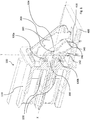
- Figure 1 shows a perspective, view of a network connector assembly 100
- the network connector assembly 100 comprises a header housing 110, comprising at least two pins 120a, 120b, forming a pin pair 122.
- a first pin end portion 130 of each of the at least two pins 120a, 120b are adapted to be connected to a counter connector along a mating axis X.
- a second pin end portion 140 of each of the at least two pins 120a, 120b is adapted to be connected to a PCB 400.
- the second pin end portions 140 extend perpendicular to the mating axis X.
- the second pin end portions 140 comprise at least one press protrusion 142, protruding perpendicular from the second pin end portions 140, adapted to cooperate with a press tool, while being pressed in a PCB-opening 410 of the PCB.
- a first electrically conductive shielding member 200 arranged lateral to the pin pair 122, shielding the pin pair 122 on at least one side.
- a second electrically conductive shielding member 300 arranged in between the at least two pins 120a, 120b of the pin pair 122, shielding the at least two pins 120a, 120b from each other.
- the second electrically conductive shielding member 300 is insulated from the PCB and electrically connected only to the first shielding member 200.
- the second electrically conductive shielding member 300 comprises a tool opening 310.
- the tool opening 310 is arranged at a position that allows movement of a press tool 500 ( figure 5 ) through the tool opening 310 along a tool axis T, to access the press protrusion 142.
- the second pin end portions 140 form a press fit connector adapted to connect to the PCB 400.
- Figure 2 shows a perspective, side view of a network connector assembly.
- the second electrically conductive shielding member 300 provides shielding between the two pins 120a, 120b of the pin pair 230 along the second electrically conductive shielding member 300.
- the second electrically conductive shielding member 300 provides a continuous line of shielding material between the two pins 120a, 120b.
- the tool opening 310 is spaced away from the continuous line.
- the first shielding member 200 comprises a substantially flat first shielding plate 210, arranged parallel to the mating axis X.
- the second shielding member 300 comprises a second shielding plate 310, arranged perpendicular to the first shielding plate, having a substantially flat internal shielding portion 312, arranged along the mating axis X and a substantially flat external shielding portion 314, angled with respect to the internal shielding portion 312.
- the second shielding member 300 could also have a third substantially flat external shielding portion along the tool axis T. In which case the second shielding member 300 could have his own end portions for connection with a PCB-opening of the PCB 400.
- the substantially flat internal shielding portion 312 is at least partly in intimate contact with the header housing 110 and whereby the external shielding portion 314 protrudes outside the header housing 110 providing flexible movement.
- One of the at least two pins 120a, 120b comprises an intermediate pin portion 124 arranged between the first pin end portion 130 and the second pin end portion 140, whereby the intermediate pin portion 124 is straight in shape and connected to the first pin end portion 130 defining an angle ⁇ 90° and connected to the second pin end portion 140 defining an angle ⁇ 90°.
- the end portions 130 and 140 could also be linked with a single radius (quarter of a circle).
- the first pin end portion 130 and the second pin end portion 140 of the other of the at least two pins 120a, 120b are connected defining an angle of 90°.
- the plane external shielding portion 314, is angled to extend parallel to the intermediate pin portion 124.
- Figure 3 shows a perspective, view to the intermediate pin portion of a network connector assembly.
- the first shielding plate 210 comprises a grounding bulge 220 protruding from the first shielding plate 210 towards the external shielding portion 314 and whereby the external shielding portion 314 is arranged lateral and in contact with the grounding bulge 220, connecting the first shielding plate 210 and the second shielding plate 310 electrically.
- the tool opening 310 is arranged at least partly in an area of the second shielding plate 310 where the internal shielding portion 312 and the external shielding portion 314 are connected.
- the intermediate pin portion 124 varies in width along the way from the first pin end portion 130 to the second pin end portion 140 to enable the tool 500 to access the press protrusion 412.
- the network connector assembly 100 is mounted on a printed circuit board PCB 400.
- the first shielding member 200 comprises a contacting member 230 for electrically conductive contacting the shielding member 200 with conductive traces 420 on the printed circuit board 400.
- the first shielding member 200 comprises also a ground press protrusion 240 to for pressing the contacting member 230 into an opening of the PCB. Parts of the second pin end portions 140 are received in the PCB-opening 410 of the PCB.
- Figure 4 shows a perspective, view of a network connector assembly 100 with six pin pairs 122 in a row. Only one row of the pins (pin 120a) is visible because the other pins (pin 120b) are covered by the external shielding portion 314. Between two pin pairs (120a, 120b) a first electrically conductive shielding member 200 is arranged. On the ends of the row, third electrically conductive shielding members 260 are arranged lateral to the pin pairs 122 and opposite to the first electrically conductive shielding members 200, thereby shielding the pin pairs 122 on the other sides.
- the third shielding plate 260 comprises a grounding bulge 262 protruding from the third shielding plate 260 towards the external shielding portion 314 and whereby the external shielding portion 314 is arranged lateral and in contact with the grounding bulge 262, connecting the third shielding plate 260 and the second shielding plate 310 electrically.
- Figure 5 shows a perspective, view of network connector assembly with the press tool 500.
- the press tool 500 is at the end of the motion towards the PCB.
- Parts of the second end portions 140 protrude through the PCB-openings 410.
- Contact means (not shown) inside the PCB-opening 410 contact the second end portions 140 with the conductive traces on the PCB 400.
Landscapes
- Engineering & Computer Science (AREA)
- Manufacturing & Machinery (AREA)
- Details Of Connecting Devices For Male And Female Coupling (AREA)
Abstract
Description
- The invention relates to a network connector assembly, in particular for vehicles, wherein the network connector assembly is suitable for networks communicating at data rates at 100 Mbit/s and/or 1 Gbit/s.
- In recent years, vehicles have been equipped with numerous on board electronics. These on board electronics provide a wide field of functionality, such as sensors, control functions and the like. For data communication between single on board electronic components, data networks have been established within vehicles. These data networks are, for example, based on Ethernet operating at data rates up to 100 Mbits/s and/or 1 Gbit/s.
- With providing new on board electronics, the need for higher data rates increases. However, the higher the data rate, the higher is the crosstalk level, particularly if connectors and/or cables of single data signal paths are arranged adjacent to each other. Further, with increasing data rates, the EMC properties (electromagnetic compatibility) of the connectors used decreases. Thus, different connectors are provided for 100 Mbit/s networks and 1 Gbit/s networks. To overcome increased crosstalk and reduced EMC properties at data rates up to 1 Gbit/s, shielding means provided in the connector housings are necessary in order to maintain the packaging / pitches. The connection to a printed circuit board (PCB) is usually established by solder the pins of the connector to the metallic layer of the PCB. This process is demanding because the solder parameters have to be well controlled. The process also requires an amount of time to provide good electrical connections.
- Thus, there is the need in the art to provide a network connector that is suitable to transfer signals with data rates of at least 1 Gbit/s and can be assembled in a fast and reliable assembly process to a PCB thereby having good electrically connectivity as well as good crosstalk and EMC properties.
- Therefore, in one aspect, the present invention improves the state of the art by providing a network connector assembly that can be assembled in a fast and reliable assembly process to a PCB thereby having good electrically connectivity as well as good crosstalk and EMC properties.
- These and other objects which become apparent upon reading the following description are solved by a network connector assembly according to independent claim 1 and a method to assemble the network connector assembly to a PCB according to independent claim 15.
- The present application relates to a network connector assembly, in particular for vehicles. The network preferably communicates at data rates of at least 100 Mbit/s and/or at least 1 Gbit/s. The network connector assembly comprises a header housing , comprising at least two pins , forming a pin pair, wherein a first pin end portion of each of the at least two pins are adapted to be connected to a counter connector along a mating axis. A second pin end portion of each of the at least two pins is adapted to be connected to a PCB. The second pin end portions extend perpendicular to the mating axis. A first electrically conductive shielding member, arranged lateral to the pin pair, shielding the pin pair on at least one side and a second electrically conductive shielding member, arranged in between the at least two pins of the pin pair, shielding the at least two pins from each other. The second pin end portions form a press fit connector adapted to connect to the PCB. The second pin end portions comprise at least one press protrusion, protruding perpendicular from the second pin end portions, adapted to cooperate with a press tool, while being pressed in a PCB-opening of the PCB. The second electrically conductive shielding member comprises a tool opening, whereby the tool opening is arranged at a position that allows movement of a press tool through the tool opening along a tool axis, to access the press protrusion.
- The disclosed invention provides an opportunity to connect the pins of the network connector assembly to the conductive layer of the PCB by using press fit technology. Press-fit technology is widely used in the art. The principle for a press-fit connection is that a contact terminal is pressed into a printed circuit board (PCB). There are two types of press-fit pins; the solid pin having a solid press-in zone and the compliant pin having an elastic press-in zone. The disclosed invention is able to use both types of press-fit pins. While using preassembled, shielded network connector assemblies it is difficult to connect the network connector assembly to the PCB because the press-fit pins are covered in a wide range of the shielding means. A necessary press in tool can't engage the press-fit pins to force them into openings of the PCB. The solution of this problem is to provide openings in the shielding means that allow access to the press-fit pins. But the openings in the shielding means have to be placed carefully to not destroy the shielding ability.
- The present application further relates to a Method to assemble a network connector assembly to a PCB. The method comprises the steps:
- providing a network connector assembly;
- providing a PCB;
- providing a tool
- adjusting the network connector assembly on the PCB thereby positioning the second pin end portion over the PCB opening of the PCB;
- aligning the tool to the network connector assembly;
- pressing the second pin end portion into the PCB opening using the tool;
- removing the tool.
- While conducting the step, pressing the second pin end portion into the PCB-opening using the tool, either the network connector assembly is moved towards the PCB or the PCB is moved towards the network connector assembly.
- According to a preferred embodiment the second electrically conductive shielding member provides shielding between the two pins of the pin pair along the second electrically conductive shielding member. Wherein an imaginary linear line between the pins intersects with the second electrically conductive shielding member and the position of the tool opening is spaced away from this intersection. In other words, the pins do not see each other. The tool opening is spaced away from line of sights of the pins. As long as the pins are not visible to each other the shielding works quite well.
- Preferably the first shielding member comprises a substantially flat first shielding plate, arranged parallel to the mating axis and wherein the second shielding member comprises a second shielding plate, arranged perpendicular to the first shielding plate, having a substantially flat internal shielding portion, arranged along the mating axis and a substantially flat external shielding portion, angled with respect to the internal shielding portion.
- The first shielding plate and the second shielding plate are arranged perpendicular to each other forming a T shape in cross-section. The external shielding portion is angled to keep the distance to the angled connector pins thereby providing continues shielding. The first shielding plate in the second shielding plate are usually made from sheet metal but can also be made of conductive plastics.
- Advantageously, the substantially plane internal shielding portion is at least partly in intimate contact with the header housing and whereby the external shielding portion protrudes outside the header housing providing flexible movement. The internal shielding portion can be captured in a cavity of the header housing. In another embodiment the internal shielding portion can be fixed inside the header housing while molding the header housing. The external shielding portion is able to cooperate with rigid protrusion by moving flexible when coming in engagement with them. That makes the design of counter contacts easier.
- Preferably the first shielding plate comprises a grounding bulge protruding from the first shielding plate towards the external shielding portion and whereby the external shielding portion is arranged lateral and in contact with the grounding bulge, connecting the first shielding plate and the second shielding plate electrically. Because no cuts in the first shielding plate are necessary to provide a grounding contact the first shielding plate keeps a closed surface and provides best shielding performance. The grounding bulge can be pressed into the first shielding plate with a tool. This flexible contact between the grounding bulge and the second shielding plate provides reliable contact over a lifetime.
- Advantageously, the tool opening is arranged at least partly in an area of the second shielding plate where the internal shielding portion and the external shielding portion are connected. Providing the tool opening in the region where the second shielding plate is bend, makes the bending process easier because on the bending edge is less material.
- Preferably, one of the at least two pins comprises an intermediate pin portion arranged between the first pin end portion and the second pin end portion, whereby the intermediate pin portion is straight in shape and connected to the first pin end portion defining an angle < 90° and connected to the second pin end portion defining an angle < 90°, whereby the first pin end portion and the second pin end portion of the other of the at least two pins, are connected defining an angle of 90°. The usage of an intermediate pin portion is necessary to adapt the two signal paths of high-speed data transfer to the different geometry of the two pins of the network connector assembly.
- Preferably the plane external shielding portion, is angled to extend parallel to the intermediate pin portion
- In a preferred embodiment, the intermediate pin portion varies in width along the way from the first pin end portion to the second pin end portion. The intermediate pin portion extends parallel to the external shielding portion of the second shielding plate to keep the impedance of the signal path constant.
- Advantageously, the network connector assembly is mounted on a printed circuit board (PCB) and wherein the first shielding member comprises a contacting member for electrically conductive contacting the shielding member with the printed circuit board. The contacting member can also be designed as a press-fit connection. The contacting member can be pressed into the PCB at the same time when the contact pins are pressed in. That makes it possible to connect the network connector assembly in one step to the PCB.
- Advantageously, parts of the second pin end portions are received in the PCB opening of the PCB. The parts of the second pin end portions that are received in the PCB openings make contact to conductive sleeves arranged inside the PCB-openings.
- Preferably the second electrically conductive shielding member is insulated from the PCB and electrically connected only to the first shielding member. The second electrically conductive shielding member does not need an electrical connection to the PCB. That saves space on the PCB where usually contact points for connecting the shielding are required.
- Preferably the network connector assembly comprising a third electrically conductive shielding member arranged lateral to the pin pair, opposite to the first electrically conductive shielding member thereby shielding the pin pair on the other side. Additional shielding members improve the robustness of the data transfer while using high data rates. The pin pairs are surrounded on a high amount of shielding members that prevent interferences with other pin pairs.
- Advantageously, the third shielding plate comprises a grounding bulge protruding from the third shielding plate towards the external shielding portion and whereby the external shielding portion is arranged lateral and in contact with the grounding bulge, connecting the third shielding plate and the second shielding plate electrically. As described for the first shielding plate the grounding bulge can be pressed into the third shielding plate with a tool. This design needs only one grounding point between shielding member and the PCB to provide a complete shielding of the network connector assembly.
- It is also foreseen to have a network connector assembly according to claim 15, wherein the first shielding plate provides a grounding bulge that engages with the external shielding portion to keep it in place. This has the advantage that improved shielding continuity between the horizontal shield and the vertical shield is provided in an easy to manufacture manner. As the vertical shield comprises for example bulges or embossments that are easy to create, there is no need for complicated stamping tools or attachment means between the external shielding portion and the first shielding plate. Moreover, as the external shielding portion is bended, a pre-spring force in the external shielding portion may be used to abut to the grounding bulge to provide an efficient shielding continuity in an easy to manufacture manner.
- It is also foreseen that the invention according claim 15 may be combined with all the embodiments of network connector assemblies as described above.
- A Network connector assembly, in particular for vehicles, wherein the network preferably communicates at data rates of at least 100 Mbit/s and/or at least 1 Gbit/s. The network connector assembly comprises a header housing and a first electrically conductive shielding member, arranged lateral to a second electrically conductive shielding member. The first shielding member comprises a substantially flat first shielding plate, arranged parallel to a mating axis of the connector assembly. The second shielding member comprises a second shielding plate , arranged perpendicular to the first shielding plate, having a substantially flat internal shielding portion, arranged along the mating axis and a substantially plane external shielding portion, angled with respect to the internal shielding portion. The substantially plane internal shielding portion is at least partly in intimate contact with the header housing. The external shielding portion protrudes outside the header housing providing flexible movement. The first shielding plate comprises a grounding bulge protruding from the first shielding plate towards the external shielding portion. The external shielding portion is arranged lateral and in contact with the grounding bulge, connecting the first shielding plate and the second shielding plate electrically.
- In the following, the invention is described exemplarily with reference to the enclosed figures, in which
- Fig. 1
- shows a perspective, view of a cut network connector assembly;
- Fig. 2
- shows a perspective, side view of a cut Network connector assembly;
- Fig. 3
- shows a perspective, view to the intermediate pin portion of a Network connector assembly;
- Fig. 4
- shows a perspective, view of details of the intermediate pin portion, the first electrically conductive shielding member and the PCB;
- Fig. 5
- shows a perspective, view of Network connector assembly with the press tool;
-
Figure 1 shows a perspective, view of anetwork connector assembly 100, Thenetwork connector assembly 100 comprises aheader housing 110, comprising at least twopins pin pair 122. A firstpin end portion 130 of each of the at least twopins pin end portion 140 of each of the at least twopins PCB 400. The secondpin end portions 140 extend perpendicular to the mating axis X. The secondpin end portions 140 comprise at least onepress protrusion 142, protruding perpendicular from the secondpin end portions 140, adapted to cooperate with a press tool, while being pressed in a PCB-opening 410 of the PCB. A first electricallyconductive shielding member 200, arranged lateral to thepin pair 122, shielding thepin pair 122 on at least one side. A second electricallyconductive shielding member 300, arranged in between the at least twopins pin pair 122, shielding the at least twopins conductive shielding member 300 is insulated from the PCB and electrically connected only to thefirst shielding member 200. The second electricallyconductive shielding member 300 comprises atool opening 310. Thetool opening 310 is arranged at a position that allows movement of a press tool 500 (figure 5 ) through thetool opening 310 along a tool axis T, to access thepress protrusion 142. The secondpin end portions 140 form a press fit connector adapted to connect to thePCB 400. -
Figure 2 shows a perspective, side view of a network connector assembly. The second electricallyconductive shielding member 300 provides shielding between the twopins pin pair 230 along the second electricallyconductive shielding member 300. The second electricallyconductive shielding member 300 provides a continuous line of shielding material between the twopins tool opening 310 is spaced away from the continuous line. Thefirst shielding member 200 comprises a substantially flatfirst shielding plate 210, arranged parallel to the mating axis X. Thesecond shielding member 300 comprises asecond shielding plate 310, arranged perpendicular to the first shielding plate, having a substantially flatinternal shielding portion 312, arranged along the mating axis X and a substantially flatexternal shielding portion 314, angled with respect to theinternal shielding portion 312. Although for cost reasons not a feature of the preferred embodiment, thesecond shielding member 300 could also have a third substantially flat external shielding portion along the tool axis T. In which case thesecond shielding member 300 could have his own end portions for connection with a PCB-opening of thePCB 400. The substantially flatinternal shielding portion 312 is at least partly in intimate contact with theheader housing 110 and whereby theexternal shielding portion 314 protrudes outside theheader housing 110 providing flexible movement. One of the at least twopins intermediate pin portion 124 arranged between the firstpin end portion 130 and the secondpin end portion 140, whereby theintermediate pin portion 124 is straight in shape and connected to the firstpin end portion 130 defining an angle < 90° and connected to the secondpin end portion 140 defining an angle < 90°. Although for manufacturability not a feature of the preferred embodiment, theend portions pin end portion 130 and the secondpin end portion 140 of the other of the at least twopins external shielding portion 314, is angled to extend parallel to theintermediate pin portion 124. -
Figure 3 shows a perspective, view to the intermediate pin portion of a network connector assembly. Thefirst shielding plate 210 comprises agrounding bulge 220 protruding from thefirst shielding plate 210 towards theexternal shielding portion 314 and whereby theexternal shielding portion 314 is arranged lateral and in contact with thegrounding bulge 220, connecting thefirst shielding plate 210 and thesecond shielding plate 310 electrically. Thetool opening 310 is arranged at least partly in an area of thesecond shielding plate 310 where theinternal shielding portion 312 and theexternal shielding portion 314 are connected. Theintermediate pin portion 124 varies in width along the way from the firstpin end portion 130 to the secondpin end portion 140 to enable thetool 500 to access the press protrusion 412. Thenetwork connector assembly 100 is mounted on a printedcircuit board PCB 400. Thefirst shielding member 200 comprises a contactingmember 230 for electrically conductive contacting the shieldingmember 200 withconductive traces 420 on the printedcircuit board 400. Thefirst shielding member 200 comprises also aground press protrusion 240 to for pressing the contactingmember 230 into an opening of the PCB. Parts of the secondpin end portions 140 are received in the PCB-opening 410 of the PCB. -
Figure 4 shows a perspective, view of anetwork connector assembly 100 with six pin pairs 122 in a row. Only one row of the pins (pin 120a) is visible because the other pins (pin 120b) are covered by theexternal shielding portion 314. Between two pin pairs (120a, 120b) a first electricallyconductive shielding member 200 is arranged. On the ends of the row, third electricallyconductive shielding members 260 are arranged lateral to the pin pairs 122 and opposite to the first electricallyconductive shielding members 200, thereby shielding the pin pairs 122 on the other sides. Thethird shielding plate 260 comprises agrounding bulge 262 protruding from thethird shielding plate 260 towards theexternal shielding portion 314 and whereby theexternal shielding portion 314 is arranged lateral and in contact with thegrounding bulge 262, connecting thethird shielding plate 260 and thesecond shielding plate 310 electrically. -
Figure 5 shows a perspective, view of network connector assembly with thepress tool 500. Thepress tool 500 is at the end of the motion towards the PCB. Parts of thesecond end portions 140 protrude through the PCB-openings 410. Contact means (not shown) inside the PCB-opening 410 contact thesecond end portions 140 with the conductive traces on thePCB 400.
Claims (16)
- Network connector assembly (100), in particular for vehicles, wherein the network preferably communicates at data rates of at least 100 Mbit/s and/or at least 1 Gbit/s, and wherein the network connector assembly (100) comprises a header housing (110), comprising at least two pins (120a, 120b), forming a pin pair (122), wherein a first pin end portion (130) of each of the at least two pins (120a, 120b) are adapted to be connected to a counter connector along a mating axis (X) and wherein a second pin end portion (140) of each of the at least two pins (120a, 120b) is adapted to be connected to a PCB (400), whereby the second pin end portions (140) extend perpendicular to the mating axis (X); a first electrically conductive shielding member (200), arranged lateral to the pin pair (122), shielding the pin pair (122) on at least one side and a second electrically conductive shielding member (300), arranged in between the at least two pins (120a, 120b) of the pin pair (122), shielding the at least two pins (120a, 120b) from each other, wherein the second pin end portions (140) form a press fit connector adapted to connect to the PCB (400), whereby the second pin end portions (140) comprise at least one press protrusion (142), protruding perpendicular from the second pin end portions (140), adapted to cooperate with a press tool, while being pressed in a PCB-opening (410) of the PCB, whereby the second electrically conductive shielding member (300) comprises a tool opening (310), whereby the tool opening (310) is arranged at a position that allows movement of a press tool (500) through the tool opening (310) along a tool axis (T), to access the press protrusion (142).
- Network connector assembly (100) according to claim 1, wherein the second electrically conductive shielding member (300) provides shielding between the two pins (120a, 120b) of the pin pair (230) along the second electrically conductive shielding member (300).
- Network connector assembly (100) according to any preceding claim, wherein the first shielding member (200) comprises a substantially flat first shielding plate (210), arranged parallel to the mating axis (X) and wherein the second shielding member (300) comprises a second shielding plate (310), arranged perpendicular to the first shielding plate, having a substantially flat internal shielding portion (312), arranged along the mating axis (X) and a substantially plane external shielding portion (314), angled with respect to the internal shielding portion (312).
- Network connector assembly (100) according to claim 3, wherein the substantially plane internal shielding portion (312) is at least partly in intimate contact with the header housing (110) and whereby the external shielding portion (314) protrudes outside the header housing (110) providing flexible movement.
- Network connector assembly (100) according to claims 3 or 4, wherein the first shielding plate (210) comprises a grounding bulge (220) protruding from the first shielding plate (210) towards the external shielding portion (314) and whereby the external shielding portion (314) is arranged lateral and in contact with the grounding bulge (220), connecting the first shielding plate (210) and the second shielding plate (310) electrically.
- Network connector assembly (100) according to any of claims 3 to 5, wherein the tool opening (310) is arranged at least partly in an area of the second shielding plate (310) where the internal shielding portion (312) and the external shielding portion (314) are connected.
- Network connector assembly (100) according to any of claims 1 to 6, wherein one of the at least two pins (120a, 120b) comprises an intermediate pin portion (124) arranged between the first pin end portion (130) and the second pin end portion (140), whereby the intermediate pin portion (124) is straight in shape and connected to the first pin end portion (130) defining an angle < 90° and connected to the second pin end portion (140) defining an angle < 90°, whereby the first pin end portion (130) and the second pin end portion (140) of the other of the at least two pins (120a, 120b), are connected defining an angle of 90°.
- Network connector assembly (100) according to the preceding claim and claim 3, wherein the plane external shielding portion (314), is angled to extend parallel to the intermediate pin portion (124).
- Network connector assembly (100) according to any of the claims 7-9, wherein the intermediate pin portion (124) varies in width along the way from the first pin end portion (130) to the second pin end portion (140).
- Network connector assembly (100) according to any preceding claim, wherein the network connector assembly (100) is mounted on a printed circuit board (PCB) (400), and wherein the first shielding member (200) comprises a contacting member (230) for electrically conductive contacting the shielding member (200) with the printed circuit board (400).
- Network connector assembly (100) according to the preceding claim, wherein parts of the second pin end portions (140) are received in the PCB-opening (410) of the PCB.
- Network connector assembly (100) according to any of the preceding claims, wherein the second electrically conductive shielding member (300) is insulated from the PCB and electrically connected only to the first shielding member (200).
- Network connector assembly (100) according to any of the preceding claims, comprising a third electrically conductive shielding member (260) arranged lateral to the pin pair (122), opposite to the first electrically conductive shielding member (200) thereby shielding the pin pair (122) on the other side.
- Network connector assembly (100) according to the preceding claim and claims 3 or 4, wherein the third shielding plate (260) comprises a grounding bulge (262) protruding from the third shielding plate (260) towards the external shielding portion (314) and whereby the external shielding portion (314) is arranged lateral and in contact with the grounding bulge (260), connecting the third shielding plate (260) and the second shielding plate (310) electrically.
- Network connector assembly (100), in particular for vehicles, wherein the network preferably communicates at data rates of at least 100 Mbit/s and/or at least 1 Gbit/s, and wherein the network connector assembly (100) comprises a header housing (110) and a first electrically conductive shielding member (200), arranged lateral to a second electrically conductive shielding member (300), wherein the first shielding member (200) comprises a substantially flat first shielding plate (210), arranged parallel to a mating axis (X) of the connector assembly and wherein the second shielding member (300) comprises a second shielding plate (310), arranged perpendicular to the first shielding plate, having a substantially flat internal shielding portion (312), arranged along the mating axis (X) and a substantially plane external shielding portion (314), angled with respect to the internal shielding portion (312), wherein the substantially plane internal shielding portion (312) is at least partly in intimate contact with the header housing (110) and whereby the external shielding portion (314) protrudes outside the header housing (110) providing flexible movement, wherein the first shielding plate (210) comprises a grounding bulge (220) protruding from the first shielding plate (210) towards the external shielding portion (314) and whereby the external shielding portion (314) is arranged lateral and in contact with the grounding bulge (220), connecting the first shielding plate (210) and the second shielding plate (310) electrically.
- Method to assemble a Network connector assembly to a PCB (400) according claims 10 to 12, comprising the steps:- providing a network connector assembly (100) according to claim 1 to 9;- providing a PCB (400);- providing a tool (500)- adjusting the network connector assembly (100) on the PCB (400) thereby positioning the second pin end portion (140) over the PCB-opening (410) of the PCB;- aligning the tool on the network connector assembly (100);- pressing the second pin end portion (140) into the PCB-opening (410) using the tool (500);- removing the tool (500);
Priority Applications (4)
| Application Number | Priority Date | Filing Date | Title |
|---|---|---|---|
| EP17186930.8A EP3444904B1 (en) | 2017-08-18 | 2017-08-18 | Electrical connector assembly |
| US16/037,415 US10290979B2 (en) | 2017-08-18 | 2018-07-17 | Electrical connector assembly |
| KR1020180094772A KR102579028B1 (en) | 2017-08-18 | 2018-08-14 | Electrical connector assembly |
| CN201810933002.4A CN109411914B (en) | 2017-08-18 | 2018-08-16 | Network connector assembly and method of assembling the network connector assembly to a PCB |
Applications Claiming Priority (1)
| Application Number | Priority Date | Filing Date | Title |
|---|---|---|---|
| EP17186930.8A EP3444904B1 (en) | 2017-08-18 | 2017-08-18 | Electrical connector assembly |
Publications (2)
| Publication Number | Publication Date |
|---|---|
| EP3444904A1 true EP3444904A1 (en) | 2019-02-20 |
| EP3444904B1 EP3444904B1 (en) | 2021-04-14 |
Family
ID=59655993
Family Applications (1)
| Application Number | Title | Priority Date | Filing Date |
|---|---|---|---|
| EP17186930.8A Active EP3444904B1 (en) | 2017-08-18 | 2017-08-18 | Electrical connector assembly |
Country Status (4)
| Country | Link |
|---|---|
| US (1) | US10290979B2 (en) |
| EP (1) | EP3444904B1 (en) |
| KR (1) | KR102579028B1 (en) |
| CN (1) | CN109411914B (en) |
Cited By (1)
| Publication number | Priority date | Publication date | Assignee | Title |
|---|---|---|---|---|
| CN112366484A (en) * | 2020-09-10 | 2021-02-12 | 番禺得意精密电子工业有限公司 | Electric connector and connector combination with same |
Families Citing this family (1)
| Publication number | Priority date | Publication date | Assignee | Title |
|---|---|---|---|---|
| KR102588446B1 (en) | 2022-09-20 | 2023-10-13 | 주식회사 에이젠글로벌 | Method for managing battery record and apparatus for performing the method |
Citations (5)
| Publication number | Priority date | Publication date | Assignee | Title |
|---|---|---|---|---|
| EP0128306A1 (en) * | 1983-05-18 | 1984-12-19 | ERNI Elektroapparate GmbH | Blade connector plug |
| DE3925958C1 (en) * | 1989-08-05 | 1991-02-07 | Harting Elektronik Gmbh, 4992 Espelkamp, De | Plug connector insertable in metallised bores of PCB - has parallel rows of contact element at right angles to insertion direction of counter-plug for other appts. |
| EP1107400A1 (en) * | 1999-11-30 | 2001-06-13 | Molex Incorporated | Electrical connector with improved terminal configuration |
| EP1263088A1 (en) * | 2001-05-30 | 2002-12-04 | Fci | Right-angled connector |
| WO2015124482A1 (en) * | 2014-02-24 | 2015-08-27 | Robert Bosch Gmbh | Plug connection element, connecting arrangement having a plurality of plug connection elements in an electrical device and press-in tool for forming a connecting arrangement |
Family Cites Families (16)
| Publication number | Priority date | Publication date | Assignee | Title |
|---|---|---|---|---|
| US4871321A (en) * | 1988-03-22 | 1989-10-03 | Teradyne, Inc. | Electrical connector |
| US4846727A (en) * | 1988-04-11 | 1989-07-11 | Amp Incorporated | Reference conductor for improving signal integrity in electrical connectors |
| EP0729653B1 (en) * | 1993-11-15 | 2001-05-16 | Berg Electronics Manufacturing B.V. | Right angle electrical connector and insertion tool |
| DE69929613T2 (en) * | 1998-08-12 | 2006-09-28 | Robinson Nugent, Inc., New Albany | CONNECTION DEVICE |
| JP3491064B2 (en) * | 2000-10-20 | 2004-01-26 | 日本航空電子工業株式会社 | High-speed transmission connector |
| US20030166349A1 (en) * | 2002-03-01 | 2003-09-04 | Huss John P. | Pin installation guidance apparatus, methods and articles of manufacture |
| JP4331570B2 (en) * | 2003-10-29 | 2009-09-16 | モレックス インコーポレイテド | connector |
| CN2770142Y (en) * | 2004-12-25 | 2006-04-05 | 富士康(昆山)电脑接插件有限公司 | Rear panel connector |
| CN2809949Y (en) * | 2005-06-10 | 2006-08-23 | 富士康(昆山)电脑接插件有限公司 | Backboard connector |
| US7806729B2 (en) * | 2008-02-12 | 2010-10-05 | Tyco Electronics Corporation | High-speed backplane connector |
| CN102593661B (en) * | 2011-01-14 | 2014-07-02 | 富士康(昆山)电脑接插件有限公司 | Electric connector |
| US8951066B2 (en) * | 2011-07-22 | 2015-02-10 | Lear Corporation | Electrical connector |
| WO2015080997A1 (en) * | 2013-11-27 | 2015-06-04 | Fci Asia Pte. Ltd | Electrical connector including guide member |
| US9431751B2 (en) * | 2014-03-25 | 2016-08-30 | Tyco Electronics Brasil Ltda | Connector having a pin guide for use with a printed circuit board |
| WO2015183951A1 (en) * | 2014-05-30 | 2015-12-03 | Molex Incorporated | Electrical connector with terminal holder |
| US9692183B2 (en) * | 2015-01-20 | 2017-06-27 | Te Connectivity Corporation | Receptacle connector with ground bus |
-
2017
- 2017-08-18 EP EP17186930.8A patent/EP3444904B1/en active Active
-
2018
- 2018-07-17 US US16/037,415 patent/US10290979B2/en active Active
- 2018-08-14 KR KR1020180094772A patent/KR102579028B1/en active Active
- 2018-08-16 CN CN201810933002.4A patent/CN109411914B/en active Active
Patent Citations (5)
| Publication number | Priority date | Publication date | Assignee | Title |
|---|---|---|---|---|
| EP0128306A1 (en) * | 1983-05-18 | 1984-12-19 | ERNI Elektroapparate GmbH | Blade connector plug |
| DE3925958C1 (en) * | 1989-08-05 | 1991-02-07 | Harting Elektronik Gmbh, 4992 Espelkamp, De | Plug connector insertable in metallised bores of PCB - has parallel rows of contact element at right angles to insertion direction of counter-plug for other appts. |
| EP1107400A1 (en) * | 1999-11-30 | 2001-06-13 | Molex Incorporated | Electrical connector with improved terminal configuration |
| EP1263088A1 (en) * | 2001-05-30 | 2002-12-04 | Fci | Right-angled connector |
| WO2015124482A1 (en) * | 2014-02-24 | 2015-08-27 | Robert Bosch Gmbh | Plug connection element, connecting arrangement having a plurality of plug connection elements in an electrical device and press-in tool for forming a connecting arrangement |
Cited By (1)
| Publication number | Priority date | Publication date | Assignee | Title |
|---|---|---|---|---|
| CN112366484A (en) * | 2020-09-10 | 2021-02-12 | 番禺得意精密电子工业有限公司 | Electric connector and connector combination with same |
Also Published As
| Publication number | Publication date |
|---|---|
| KR20190019842A (en) | 2019-02-27 |
| CN109411914B (en) | 2020-09-18 |
| CN109411914A (en) | 2019-03-01 |
| US10290979B2 (en) | 2019-05-14 |
| EP3444904B1 (en) | 2021-04-14 |
| KR102579028B1 (en) | 2023-09-18 |
| US20190058290A1 (en) | 2019-02-21 |
Similar Documents
| Publication | Publication Date | Title |
|---|---|---|
| KR102240783B1 (en) | Electrical connector device | |
| CN111313168B (en) | Overmolded lead frame providing contact support and impedance matching characteristics | |
| US8267721B2 (en) | Electrical connector having ground plates and ground coupling bar | |
| JP7832388B2 (en) | Connectors and connector pairs | |
| CN109004398B (en) | High speed electrical connector | |
| US8113884B2 (en) | Connector | |
| JP7267186B2 (en) | Connectors and connector assemblies | |
| EP2876737B1 (en) | Connector | |
| US7651372B2 (en) | Electric connector with shields on mating housings | |
| US7632107B2 (en) | Board-to-board connector | |
| WO2016115063A1 (en) | Paddle card having shortened signal contact pads | |
| CN103842867A (en) | Electrical contact and connector | |
| US12142860B2 (en) | Connector and electronic apparatus | |
| CN112753136A (en) | Plug connector | |
| JP2001217052A (en) | Connector | |
| CN113131248B (en) | Electrical connector | |
| EP3444904B1 (en) | Electrical connector assembly | |
| CN217215360U (en) | Card edge connector | |
| TWI904677B (en) | Connector assembly and sheet metal assembly | |
| TW202610137A (en) | Connector assembly | |
| JP2026077776A (en) | Connectors and connector pairs | |
| CN119366070A (en) | Connector components |
Legal Events
| Date | Code | Title | Description |
|---|---|---|---|
| PUAI | Public reference made under article 153(3) epc to a published international application that has entered the european phase |
Free format text: ORIGINAL CODE: 0009012 |
|
| STAA | Information on the status of an ep patent application or granted ep patent |
Free format text: STATUS: THE APPLICATION HAS BEEN PUBLISHED |
|
| AK | Designated contracting states |
Kind code of ref document: A1 Designated state(s): AL AT BE BG CH CY CZ DE DK EE ES FI FR GB GR HR HU IE IS IT LI LT LU LV MC MK MT NL NO PL PT RO RS SE SI SK SM TR |
|
| AX | Request for extension of the european patent |
Extension state: BA ME |
|
| STAA | Information on the status of an ep patent application or granted ep patent |
Free format text: STATUS: REQUEST FOR EXAMINATION WAS MADE |
|
| 17P | Request for examination filed |
Effective date: 20190808 |
|
| RBV | Designated contracting states (corrected) |
Designated state(s): AL AT BE BG CH CY CZ DE DK EE ES FI FR GB GR HR HU IE IS IT LI LT LU LV MC MK MT NL NO PL PT RO RS SE SI SK SM TR |
|
| STAA | Information on the status of an ep patent application or granted ep patent |
Free format text: STATUS: EXAMINATION IS IN PROGRESS |
|
| 17Q | First examination report despatched |
Effective date: 20200204 |
|
| GRAP | Despatch of communication of intention to grant a patent |
Free format text: ORIGINAL CODE: EPIDOSNIGR1 |
|
| STAA | Information on the status of an ep patent application or granted ep patent |
Free format text: STATUS: GRANT OF PATENT IS INTENDED |
|
| INTG | Intention to grant announced |
Effective date: 20201030 |
|
| GRAS | Grant fee paid |
Free format text: ORIGINAL CODE: EPIDOSNIGR3 |
|
| GRAA | (expected) grant |
Free format text: ORIGINAL CODE: 0009210 |
|
| STAA | Information on the status of an ep patent application or granted ep patent |
Free format text: STATUS: THE PATENT HAS BEEN GRANTED |
|
| AK | Designated contracting states |
Kind code of ref document: B1 Designated state(s): AL AT BE BG CH CY CZ DE DK EE ES FI FR GB GR HR HU IE IS IT LI LT LU LV MC MK MT NL NO PL PT RO RS SE SI SK SM TR |
|
| REG | Reference to a national code |
Ref country code: GB Ref legal event code: FG4D |
|
| REG | Reference to a national code |
Ref country code: CH Ref legal event code: EP |
|
| REG | Reference to a national code |
Ref country code: DE Ref legal event code: R096 Ref document number: 602017036564 Country of ref document: DE |
|
| REG | Reference to a national code |
Ref country code: IE Ref legal event code: FG4D |
|
| REG | Reference to a national code |
Ref country code: AT Ref legal event code: REF Ref document number: 1383292 Country of ref document: AT Kind code of ref document: T Effective date: 20210515 |
|
| REG | Reference to a national code |
Ref country code: LT Ref legal event code: MG9D |
|
| REG | Reference to a national code |
Ref country code: AT Ref legal event code: MK05 Ref document number: 1383292 Country of ref document: AT Kind code of ref document: T Effective date: 20210414 |
|
| REG | Reference to a national code |
Ref country code: NL Ref legal event code: MP Effective date: 20210414 |
|
| PG25 | Lapsed in a contracting state [announced via postgrant information from national office to epo] |
Ref country code: HR Free format text: LAPSE BECAUSE OF FAILURE TO SUBMIT A TRANSLATION OF THE DESCRIPTION OR TO PAY THE FEE WITHIN THE PRESCRIBED TIME-LIMIT Effective date: 20210414 Ref country code: AT Free format text: LAPSE BECAUSE OF FAILURE TO SUBMIT A TRANSLATION OF THE DESCRIPTION OR TO PAY THE FEE WITHIN THE PRESCRIBED TIME-LIMIT Effective date: 20210414 Ref country code: BG Free format text: LAPSE BECAUSE OF FAILURE TO SUBMIT A TRANSLATION OF THE DESCRIPTION OR TO PAY THE FEE WITHIN THE PRESCRIBED TIME-LIMIT Effective date: 20210714 Ref country code: NL Free format text: LAPSE BECAUSE OF FAILURE TO SUBMIT A TRANSLATION OF THE DESCRIPTION OR TO PAY THE FEE WITHIN THE PRESCRIBED TIME-LIMIT Effective date: 20210414 Ref country code: FI Free format text: LAPSE BECAUSE OF FAILURE TO SUBMIT A TRANSLATION OF THE DESCRIPTION OR TO PAY THE FEE WITHIN THE PRESCRIBED TIME-LIMIT Effective date: 20210414 Ref country code: LT Free format text: LAPSE BECAUSE OF FAILURE TO SUBMIT A TRANSLATION OF THE DESCRIPTION OR TO PAY THE FEE WITHIN THE PRESCRIBED TIME-LIMIT Effective date: 20210414 |
|
| PG25 | Lapsed in a contracting state [announced via postgrant information from national office to epo] |
Ref country code: LV Free format text: LAPSE BECAUSE OF FAILURE TO SUBMIT A TRANSLATION OF THE DESCRIPTION OR TO PAY THE FEE WITHIN THE PRESCRIBED TIME-LIMIT Effective date: 20210414 Ref country code: IS Free format text: LAPSE BECAUSE OF FAILURE TO SUBMIT A TRANSLATION OF THE DESCRIPTION OR TO PAY THE FEE WITHIN THE PRESCRIBED TIME-LIMIT Effective date: 20210814 Ref country code: GR Free format text: LAPSE BECAUSE OF FAILURE TO SUBMIT A TRANSLATION OF THE DESCRIPTION OR TO PAY THE FEE WITHIN THE PRESCRIBED TIME-LIMIT Effective date: 20210715 Ref country code: PT Free format text: LAPSE BECAUSE OF FAILURE TO SUBMIT A TRANSLATION OF THE DESCRIPTION OR TO PAY THE FEE WITHIN THE PRESCRIBED TIME-LIMIT Effective date: 20210816 Ref country code: PL Free format text: LAPSE BECAUSE OF FAILURE TO SUBMIT A TRANSLATION OF THE DESCRIPTION OR TO PAY THE FEE WITHIN THE PRESCRIBED TIME-LIMIT Effective date: 20210414 Ref country code: NO Free format text: LAPSE BECAUSE OF FAILURE TO SUBMIT A TRANSLATION OF THE DESCRIPTION OR TO PAY THE FEE WITHIN THE PRESCRIBED TIME-LIMIT Effective date: 20210714 Ref country code: SE Free format text: LAPSE BECAUSE OF FAILURE TO SUBMIT A TRANSLATION OF THE DESCRIPTION OR TO PAY THE FEE WITHIN THE PRESCRIBED TIME-LIMIT Effective date: 20210414 Ref country code: RS Free format text: LAPSE BECAUSE OF FAILURE TO SUBMIT A TRANSLATION OF THE DESCRIPTION OR TO PAY THE FEE WITHIN THE PRESCRIBED TIME-LIMIT Effective date: 20210414 |
|
| REG | Reference to a national code |
Ref country code: DE Ref legal event code: R097 Ref document number: 602017036564 Country of ref document: DE |
|
| PG25 | Lapsed in a contracting state [announced via postgrant information from national office to epo] |
Ref country code: SM Free format text: LAPSE BECAUSE OF FAILURE TO SUBMIT A TRANSLATION OF THE DESCRIPTION OR TO PAY THE FEE WITHIN THE PRESCRIBED TIME-LIMIT Effective date: 20210414 Ref country code: SK Free format text: LAPSE BECAUSE OF FAILURE TO SUBMIT A TRANSLATION OF THE DESCRIPTION OR TO PAY THE FEE WITHIN THE PRESCRIBED TIME-LIMIT Effective date: 20210414 Ref country code: RO Free format text: LAPSE BECAUSE OF FAILURE TO SUBMIT A TRANSLATION OF THE DESCRIPTION OR TO PAY THE FEE WITHIN THE PRESCRIBED TIME-LIMIT Effective date: 20210414 Ref country code: ES Free format text: LAPSE BECAUSE OF FAILURE TO SUBMIT A TRANSLATION OF THE DESCRIPTION OR TO PAY THE FEE WITHIN THE PRESCRIBED TIME-LIMIT Effective date: 20210414 Ref country code: EE Free format text: LAPSE BECAUSE OF FAILURE TO SUBMIT A TRANSLATION OF THE DESCRIPTION OR TO PAY THE FEE WITHIN THE PRESCRIBED TIME-LIMIT Effective date: 20210414 Ref country code: DK Free format text: LAPSE BECAUSE OF FAILURE TO SUBMIT A TRANSLATION OF THE DESCRIPTION OR TO PAY THE FEE WITHIN THE PRESCRIBED TIME-LIMIT Effective date: 20210414 Ref country code: CZ Free format text: LAPSE BECAUSE OF FAILURE TO SUBMIT A TRANSLATION OF THE DESCRIPTION OR TO PAY THE FEE WITHIN THE PRESCRIBED TIME-LIMIT Effective date: 20210414 |
|
| PLBE | No opposition filed within time limit |
Free format text: ORIGINAL CODE: 0009261 |
|
| STAA | Information on the status of an ep patent application or granted ep patent |
Free format text: STATUS: NO OPPOSITION FILED WITHIN TIME LIMIT |
|
| 26N | No opposition filed |
Effective date: 20220117 |
|
| REG | Reference to a national code |
Ref country code: CH Ref legal event code: PL |
|
| PG25 | Lapsed in a contracting state [announced via postgrant information from national office to epo] |
Ref country code: MC Free format text: LAPSE BECAUSE OF FAILURE TO SUBMIT A TRANSLATION OF THE DESCRIPTION OR TO PAY THE FEE WITHIN THE PRESCRIBED TIME-LIMIT Effective date: 20210414 |
|
| REG | Reference to a national code |
Ref country code: BE Ref legal event code: MM Effective date: 20210831 |
|
| PG25 | Lapsed in a contracting state [announced via postgrant information from national office to epo] |
Ref country code: LI Free format text: LAPSE BECAUSE OF NON-PAYMENT OF DUE FEES Effective date: 20210831 Ref country code: CH Free format text: LAPSE BECAUSE OF NON-PAYMENT OF DUE FEES Effective date: 20210831 |
|
| PG25 | Lapsed in a contracting state [announced via postgrant information from national office to epo] |
Ref country code: IS Free format text: LAPSE BECAUSE OF FAILURE TO SUBMIT A TRANSLATION OF THE DESCRIPTION OR TO PAY THE FEE WITHIN THE PRESCRIBED TIME-LIMIT Effective date: 20210814 Ref country code: LU Free format text: LAPSE BECAUSE OF NON-PAYMENT OF DUE FEES Effective date: 20210818 Ref country code: AL Free format text: LAPSE BECAUSE OF FAILURE TO SUBMIT A TRANSLATION OF THE DESCRIPTION OR TO PAY THE FEE WITHIN THE PRESCRIBED TIME-LIMIT Effective date: 20210414 |
|
| PG25 | Lapsed in a contracting state [announced via postgrant information from national office to epo] |
Ref country code: IT Free format text: LAPSE BECAUSE OF FAILURE TO SUBMIT A TRANSLATION OF THE DESCRIPTION OR TO PAY THE FEE WITHIN THE PRESCRIBED TIME-LIMIT Effective date: 20210414 Ref country code: IE Free format text: LAPSE BECAUSE OF NON-PAYMENT OF DUE FEES Effective date: 20210818 Ref country code: BE Free format text: LAPSE BECAUSE OF NON-PAYMENT OF DUE FEES Effective date: 20210831 |
|
| P01 | Opt-out of the competence of the unified patent court (upc) registered |
Effective date: 20230424 |
|
| PG25 | Lapsed in a contracting state [announced via postgrant information from national office to epo] |
Ref country code: CY Free format text: LAPSE BECAUSE OF FAILURE TO SUBMIT A TRANSLATION OF THE DESCRIPTION OR TO PAY THE FEE WITHIN THE PRESCRIBED TIME-LIMIT Effective date: 20210414 |
|
| PG25 | Lapsed in a contracting state [announced via postgrant information from national office to epo] |
Ref country code: HU Free format text: LAPSE BECAUSE OF FAILURE TO SUBMIT A TRANSLATION OF THE DESCRIPTION OR TO PAY THE FEE WITHIN THE PRESCRIBED TIME-LIMIT; INVALID AB INITIO Effective date: 20170818 |
|
| PG25 | Lapsed in a contracting state [announced via postgrant information from national office to epo] |
Ref country code: MK Free format text: LAPSE BECAUSE OF FAILURE TO SUBMIT A TRANSLATION OF THE DESCRIPTION OR TO PAY THE FEE WITHIN THE PRESCRIBED TIME-LIMIT Effective date: 20210414 |
|
| PG25 | Lapsed in a contracting state [announced via postgrant information from national office to epo] |
Ref country code: MT Free format text: LAPSE BECAUSE OF FAILURE TO SUBMIT A TRANSLATION OF THE DESCRIPTION OR TO PAY THE FEE WITHIN THE PRESCRIBED TIME-LIMIT Effective date: 20210414 |
|
| REG | Reference to a national code |
Ref country code: DE Ref legal event code: R081 Ref document number: 602017036564 Country of ref document: DE Owner name: APTIV TECHNOLOGIES AG, CH Free format text: FORMER OWNER: APTIV TECHNOLOGIES LIMITED, ST. MICHAEL, BB |
|
| PGFP | Annual fee paid to national office [announced via postgrant information from national office to epo] |
Ref country code: DE Payment date: 20250722 Year of fee payment: 9 |
|
| PGFP | Annual fee paid to national office [announced via postgrant information from national office to epo] |
Ref country code: GB Payment date: 20250818 Year of fee payment: 9 |
|
| PGFP | Annual fee paid to national office [announced via postgrant information from national office to epo] |
Ref country code: FR Payment date: 20250812 Year of fee payment: 9 |
|
| PG25 | Lapsed in a contracting state [announced via postgrant information from national office to epo] |
Ref country code: TR Free format text: LAPSE BECAUSE OF FAILURE TO SUBMIT A TRANSLATION OF THE DESCRIPTION OR TO PAY THE FEE WITHIN THE PRESCRIBED TIME-LIMIT Effective date: 20210414 |