EP3444838A1 - Semiconductor package including a semiconductor die whose faces are all covered with molding material and related methods - Google Patents
Semiconductor package including a semiconductor die whose faces are all covered with molding material and related methods Download PDFInfo
- Publication number
- EP3444838A1 EP3444838A1 EP18184165.1A EP18184165A EP3444838A1 EP 3444838 A1 EP3444838 A1 EP 3444838A1 EP 18184165 A EP18184165 A EP 18184165A EP 3444838 A1 EP3444838 A1 EP 3444838A1
- Authority
- EP
- European Patent Office
- Prior art keywords
- wafer
- die
- notches
- mold compound
- layer
- Prior art date
- Legal status (The legal status is an assumption and is not a legal conclusion. Google has not performed a legal analysis and makes no representation as to the accuracy of the status listed.)
- Granted
Links
Images


Classifications
-
- H—ELECTRICITY
- H10—SEMICONDUCTOR DEVICES; ELECTRIC SOLID-STATE DEVICES NOT OTHERWISE PROVIDED FOR
- H10P—GENERIC PROCESSES OR APPARATUS FOR THE MANUFACTURE OR TREATMENT OF DEVICES COVERED BY CLASS H10
- H10P50/00—Etching of wafers, substrates or parts of devices
-
- H—ELECTRICITY
- H10—SEMICONDUCTOR DEVICES; ELECTRIC SOLID-STATE DEVICES NOT OTHERWISE PROVIDED FOR
- H10P—GENERIC PROCESSES OR APPARATUS FOR THE MANUFACTURE OR TREATMENT OF DEVICES COVERED BY CLASS H10
- H10P54/00—Cutting or separating of wafers, substrates or parts of devices
-
- H—ELECTRICITY
- H10—SEMICONDUCTOR DEVICES; ELECTRIC SOLID-STATE DEVICES NOT OTHERWISE PROVIDED FOR
- H10W—GENERIC PACKAGES, INTERCONNECTIONS, CONNECTORS OR OTHER CONSTRUCTIONAL DETAILS OF DEVICES COVERED BY CLASS H10
- H10W70/00—Package substrates; Interposers; Redistribution layers [RDL]
- H10W70/60—Insulating or insulated package substrates; Interposers; Redistribution layers
-
- H—ELECTRICITY
- H10—SEMICONDUCTOR DEVICES; ELECTRIC SOLID-STATE DEVICES NOT OTHERWISE PROVIDED FOR
- H10W—GENERIC PACKAGES, INTERCONNECTIONS, CONNECTORS OR OTHER CONSTRUCTIONAL DETAILS OF DEVICES COVERED BY CLASS H10
- H10W72/00—Interconnections or connectors in packages
- H10W72/30—Die-attach connectors
-
- H—ELECTRICITY
- H10—SEMICONDUCTOR DEVICES; ELECTRIC SOLID-STATE DEVICES NOT OTHERWISE PROVIDED FOR
- H10W—GENERIC PACKAGES, INTERCONNECTIONS, CONNECTORS OR OTHER CONSTRUCTIONAL DETAILS OF DEVICES COVERED BY CLASS H10
- H10W72/00—Interconnections or connectors in packages
- H10W72/90—Bond pads, in general
-
- H—ELECTRICITY
- H10—SEMICONDUCTOR DEVICES; ELECTRIC SOLID-STATE DEVICES NOT OTHERWISE PROVIDED FOR
- H10W—GENERIC PACKAGES, INTERCONNECTIONS, CONNECTORS OR OTHER CONSTRUCTIONAL DETAILS OF DEVICES COVERED BY CLASS H10
- H10W74/00—Encapsulations, e.g. protective coatings
- H10W74/01—Manufacture or treatment
- H10W74/014—Manufacture or treatment using batch processing
-
- H—ELECTRICITY
- H10—SEMICONDUCTOR DEVICES; ELECTRIC SOLID-STATE DEVICES NOT OTHERWISE PROVIDED FOR
- H10W—GENERIC PACKAGES, INTERCONNECTIONS, CONNECTORS OR OTHER CONSTRUCTIONAL DETAILS OF DEVICES COVERED BY CLASS H10
- H10W74/00—Encapsulations, e.g. protective coatings
- H10W74/01—Manufacture or treatment
- H10W74/016—Manufacture or treatment using moulds
-
- H—ELECTRICITY
- H10—SEMICONDUCTOR DEVICES; ELECTRIC SOLID-STATE DEVICES NOT OTHERWISE PROVIDED FOR
- H10W—GENERIC PACKAGES, INTERCONNECTIONS, CONNECTORS OR OTHER CONSTRUCTIONAL DETAILS OF DEVICES COVERED BY CLASS H10
- H10W74/00—Encapsulations, e.g. protective coatings
- H10W74/10—Encapsulations, e.g. protective coatings characterised by their shape or disposition
- H10W74/111—Encapsulations, e.g. protective coatings characterised by their shape or disposition the semiconductor body being completely enclosed
- H10W74/127—Encapsulations, e.g. protective coatings characterised by their shape or disposition the semiconductor body being completely enclosed characterised by arrangements for sealing or adhesion
-
- H—ELECTRICITY
- H10—SEMICONDUCTOR DEVICES; ELECTRIC SOLID-STATE DEVICES NOT OTHERWISE PROVIDED FOR
- H10W—GENERIC PACKAGES, INTERCONNECTIONS, CONNECTORS OR OTHER CONSTRUCTIONAL DETAILS OF DEVICES COVERED BY CLASS H10
- H10W74/00—Encapsulations, e.g. protective coatings
- H10W74/10—Encapsulations, e.g. protective coatings characterised by their shape or disposition
- H10W74/131—Encapsulations, e.g. protective coatings characterised by their shape or disposition the semiconductor body being only partially enclosed
- H10W74/141—Encapsulations, e.g. protective coatings characterised by their shape or disposition the semiconductor body being only partially enclosed the encapsulations being on at least the sidewalls of the semiconductor body
-
- H—ELECTRICITY
- H10—SEMICONDUCTOR DEVICES; ELECTRIC SOLID-STATE DEVICES NOT OTHERWISE PROVIDED FOR
- H10W—GENERIC PACKAGES, INTERCONNECTIONS, CONNECTORS OR OTHER CONSTRUCTIONAL DETAILS OF DEVICES COVERED BY CLASS H10
- H10W99/00—Subject matter not provided for in other groups of this subclass
-
- H—ELECTRICITY
- H10—SEMICONDUCTOR DEVICES; ELECTRIC SOLID-STATE DEVICES NOT OTHERWISE PROVIDED FOR
- H10W—GENERIC PACKAGES, INTERCONNECTIONS, CONNECTORS OR OTHER CONSTRUCTIONAL DETAILS OF DEVICES COVERED BY CLASS H10
- H10W72/00—Interconnections or connectors in packages
- H10W72/01—Manufacture or treatment
- H10W72/012—Manufacture or treatment of bump connectors, dummy bumps or thermal bumps
- H10W72/01221—Manufacture or treatment of bump connectors, dummy bumps or thermal bumps using local deposition
-
- H—ELECTRICITY
- H10—SEMICONDUCTOR DEVICES; ELECTRIC SOLID-STATE DEVICES NOT OTHERWISE PROVIDED FOR
- H10W—GENERIC PACKAGES, INTERCONNECTIONS, CONNECTORS OR OTHER CONSTRUCTIONAL DETAILS OF DEVICES COVERED BY CLASS H10
- H10W72/00—Interconnections or connectors in packages
- H10W72/01—Manufacture or treatment
- H10W72/012—Manufacture or treatment of bump connectors, dummy bumps or thermal bumps
- H10W72/01231—Manufacture or treatment of bump connectors, dummy bumps or thermal bumps using blanket deposition
- H10W72/01233—Manufacture or treatment of bump connectors, dummy bumps or thermal bumps using blanket deposition in liquid form, e.g. spin coating, spray coating or immersion coating
- H10W72/01235—Manufacture or treatment of bump connectors, dummy bumps or thermal bumps using blanket deposition in liquid form, e.g. spin coating, spray coating or immersion coating by plating, e.g. electroless plating or electroplating
-
- H—ELECTRICITY
- H10—SEMICONDUCTOR DEVICES; ELECTRIC SOLID-STATE DEVICES NOT OTHERWISE PROVIDED FOR
- H10W—GENERIC PACKAGES, INTERCONNECTIONS, CONNECTORS OR OTHER CONSTRUCTIONAL DETAILS OF DEVICES COVERED BY CLASS H10
- H10W72/00—Interconnections or connectors in packages
- H10W72/01—Manufacture or treatment
- H10W72/012—Manufacture or treatment of bump connectors, dummy bumps or thermal bumps
- H10W72/01251—Changing the shapes of bumps
- H10W72/01253—Changing the shapes of bumps by etching
-
- H—ELECTRICITY
- H10—SEMICONDUCTOR DEVICES; ELECTRIC SOLID-STATE DEVICES NOT OTHERWISE PROVIDED FOR
- H10W—GENERIC PACKAGES, INTERCONNECTIONS, CONNECTORS OR OTHER CONSTRUCTIONAL DETAILS OF DEVICES COVERED BY CLASS H10
- H10W72/00—Interconnections or connectors in packages
- H10W72/01—Manufacture or treatment
- H10W72/012—Manufacture or treatment of bump connectors, dummy bumps or thermal bumps
- H10W72/01251—Changing the shapes of bumps
- H10W72/01255—Changing the shapes of bumps by using masks
-
- H—ELECTRICITY
- H10—SEMICONDUCTOR DEVICES; ELECTRIC SOLID-STATE DEVICES NOT OTHERWISE PROVIDED FOR
- H10W—GENERIC PACKAGES, INTERCONNECTIONS, CONNECTORS OR OTHER CONSTRUCTIONAL DETAILS OF DEVICES COVERED BY CLASS H10
- H10W72/00—Interconnections or connectors in packages
- H10W72/01—Manufacture or treatment
- H10W72/019—Manufacture or treatment of bond pads
-
- H—ELECTRICITY
- H10—SEMICONDUCTOR DEVICES; ELECTRIC SOLID-STATE DEVICES NOT OTHERWISE PROVIDED FOR
- H10W—GENERIC PACKAGES, INTERCONNECTIONS, CONNECTORS OR OTHER CONSTRUCTIONAL DETAILS OF DEVICES COVERED BY CLASS H10
- H10W72/00—Interconnections or connectors in packages
- H10W72/01—Manufacture or treatment
- H10W72/019—Manufacture or treatment of bond pads
- H10W72/01931—Manufacture or treatment of bond pads using blanket deposition
- H10W72/01933—Manufacture or treatment of bond pads using blanket deposition in liquid form, e.g. spin coating, spray coating or immersion coating
- H10W72/01935—Manufacture or treatment of bond pads using blanket deposition in liquid form, e.g. spin coating, spray coating or immersion coating by plating, e.g. electroless plating or electroplating
-
- H—ELECTRICITY
- H10—SEMICONDUCTOR DEVICES; ELECTRIC SOLID-STATE DEVICES NOT OTHERWISE PROVIDED FOR
- H10W—GENERIC PACKAGES, INTERCONNECTIONS, CONNECTORS OR OTHER CONSTRUCTIONAL DETAILS OF DEVICES COVERED BY CLASS H10
- H10W72/00—Interconnections or connectors in packages
- H10W72/01—Manufacture or treatment
- H10W72/019—Manufacture or treatment of bond pads
- H10W72/01931—Manufacture or treatment of bond pads using blanket deposition
- H10W72/01938—Manufacture or treatment of bond pads using blanket deposition in gaseous form, e.g. by CVD or PVD
-
- H—ELECTRICITY
- H10—SEMICONDUCTOR DEVICES; ELECTRIC SOLID-STATE DEVICES NOT OTHERWISE PROVIDED FOR
- H10W—GENERIC PACKAGES, INTERCONNECTIONS, CONNECTORS OR OTHER CONSTRUCTIONAL DETAILS OF DEVICES COVERED BY CLASS H10
- H10W72/00—Interconnections or connectors in packages
- H10W72/01—Manufacture or treatment
- H10W72/019—Manufacture or treatment of bond pads
- H10W72/01951—Changing the shapes of bond pads
- H10W72/01953—Changing the shapes of bond pads by etching
-
- H—ELECTRICITY
- H10—SEMICONDUCTOR DEVICES; ELECTRIC SOLID-STATE DEVICES NOT OTHERWISE PROVIDED FOR
- H10W—GENERIC PACKAGES, INTERCONNECTIONS, CONNECTORS OR OTHER CONSTRUCTIONAL DETAILS OF DEVICES COVERED BY CLASS H10
- H10W72/00—Interconnections or connectors in packages
- H10W72/01—Manufacture or treatment
- H10W72/0198—Manufacture or treatment batch processes
-
- H—ELECTRICITY
- H10—SEMICONDUCTOR DEVICES; ELECTRIC SOLID-STATE DEVICES NOT OTHERWISE PROVIDED FOR
- H10W—GENERIC PACKAGES, INTERCONNECTIONS, CONNECTORS OR OTHER CONSTRUCTIONAL DETAILS OF DEVICES COVERED BY CLASS H10
- H10W72/00—Interconnections or connectors in packages
- H10W72/071—Connecting or disconnecting
- H10W72/072—Connecting or disconnecting of bump connectors
- H10W72/07251—Connecting or disconnecting of bump connectors characterised by changes in properties of the bump connectors during connecting
- H10W72/07254—Connecting or disconnecting of bump connectors characterised by changes in properties of the bump connectors during connecting changes in dispositions
-
- H—ELECTRICITY
- H10—SEMICONDUCTOR DEVICES; ELECTRIC SOLID-STATE DEVICES NOT OTHERWISE PROVIDED FOR
- H10W—GENERIC PACKAGES, INTERCONNECTIONS, CONNECTORS OR OTHER CONSTRUCTIONAL DETAILS OF DEVICES COVERED BY CLASS H10
- H10W72/00—Interconnections or connectors in packages
- H10W72/20—Bump connectors, e.g. solder bumps or copper pillars; Dummy bumps; Thermal bumps
- H10W72/221—Structures or relative sizes
- H10W72/222—Multilayered bumps, e.g. a coating on top and side surfaces of a bump core
-
- H—ELECTRICITY
- H10—SEMICONDUCTOR DEVICES; ELECTRIC SOLID-STATE DEVICES NOT OTHERWISE PROVIDED FOR
- H10W—GENERIC PACKAGES, INTERCONNECTIONS, CONNECTORS OR OTHER CONSTRUCTIONAL DETAILS OF DEVICES COVERED BY CLASS H10
- H10W72/00—Interconnections or connectors in packages
- H10W72/20—Bump connectors, e.g. solder bumps or copper pillars; Dummy bumps; Thermal bumps
- H10W72/241—Dispositions, e.g. layouts
- H10W72/247—Dispositions of multiple bumps
- H10W72/248—Top-view layouts, e.g. mirror arrays
-
- H—ELECTRICITY
- H10—SEMICONDUCTOR DEVICES; ELECTRIC SOLID-STATE DEVICES NOT OTHERWISE PROVIDED FOR
- H10W—GENERIC PACKAGES, INTERCONNECTIONS, CONNECTORS OR OTHER CONSTRUCTIONAL DETAILS OF DEVICES COVERED BY CLASS H10
- H10W72/00—Interconnections or connectors in packages
- H10W72/20—Bump connectors, e.g. solder bumps or copper pillars; Dummy bumps; Thermal bumps
- H10W72/251—Materials
- H10W72/252—Materials comprising solid metals or solid metalloids, e.g. PbSn, Ag or Cu
-
- H—ELECTRICITY
- H10—SEMICONDUCTOR DEVICES; ELECTRIC SOLID-STATE DEVICES NOT OTHERWISE PROVIDED FOR
- H10W—GENERIC PACKAGES, INTERCONNECTIONS, CONNECTORS OR OTHER CONSTRUCTIONAL DETAILS OF DEVICES COVERED BY CLASS H10
- H10W72/00—Interconnections or connectors in packages
- H10W72/20—Bump connectors, e.g. solder bumps or copper pillars; Dummy bumps; Thermal bumps
- H10W72/29—Bond pads specially adapted therefor
-
- H—ELECTRICITY
- H10—SEMICONDUCTOR DEVICES; ELECTRIC SOLID-STATE DEVICES NOT OTHERWISE PROVIDED FOR
- H10W—GENERIC PACKAGES, INTERCONNECTIONS, CONNECTORS OR OTHER CONSTRUCTIONAL DETAILS OF DEVICES COVERED BY CLASS H10
- H10W74/00—Encapsulations, e.g. protective coatings
-
- H—ELECTRICITY
- H10—SEMICONDUCTOR DEVICES; ELECTRIC SOLID-STATE DEVICES NOT OTHERWISE PROVIDED FOR
- H10W—GENERIC PACKAGES, INTERCONNECTIONS, CONNECTORS OR OTHER CONSTRUCTIONAL DETAILS OF DEVICES COVERED BY CLASS H10
- H10W74/00—Encapsulations, e.g. protective coatings
- H10W74/10—Encapsulations, e.g. protective coatings characterised by their shape or disposition
- H10W74/111—Encapsulations, e.g. protective coatings characterised by their shape or disposition the semiconductor body being completely enclosed
Definitions
- Implementations of a method of forming a semiconductor package may include forming a metal layer on a first side of a wafer, applying a first photoresist layer on the metal layer, patterning the first photoresist layer, forming electrical contacts coupled to the metal layer using the first photoresist layer, removing the first photoresist layer, etching the metal layer, and etching a plurality of notches into the first side of the wafer.
- One of a solder resist layer, a passivation layer, an interlayer, and a combination of a solder resist layer, a passivation layer, and an interlayer may be coupled to the first side of the wafer and may be covered by the first mold compound.
- a first photoresist layer 20 is formed and patterned over the metal layer 18.
- One or more electrical contacts 22 may be formed on the metal layer 18 and within the photoresist layer 20. In various implementations this may be done using various electroplating or electroless plating techniques, though deposition and etching techniques could be employed in various implementations.
- the electrical contacts 22 may be any type of electrical contact previously disclosed herein (bumps, studs, and so forth).
- the first photoresist layer 20 is removed through an ashing or solvent dissolution process and the metal layer 18 may be etched away after the electrical contacts are formed.
- the plurality of notches may be formed using, by non-limiting example, plasma etching, deep-reactive ion etching, or wet chemical etching.
- a process marketed under the tradename BOSCH® by Robert Bosch GmbH, Stuttgart Germany (the "Bosch process"), may be used to form the plurality of notches 26 in the first side 28 of the wafer 16.
- a second mold compound 62 or a laminate resin may be applied to the second side 60 of the wafer 16.
- the mold compound may be any type of mold compound disclosed herein and may be applied using any technique disclosed herein.
- FIG. 15 a fourth process flow illustrating the formation of a semiconductor package is illustrated.
- the method for forming a semiconductor package illustrated in FIG. 15 includes providing a wafer 120.
- an interlayer 122 may be coupled to a first side 124 of the wafer 120.
- a passivation layer 128 may be coupled to the wafer 120.
- the passivation layer may be any type of passivation layer disclosed herein.
- the passivation layer 128 may be patterned and may directly contact portions of the wafer 120.
- the patterned passivation layer, or mask may be used to etch a plurality of notches 138 into the first side 124 of the wafer 120 using any etching process disclosed herein.
- the plurality of notches may be etched using any method disclosed herein, and may be any type of notch previously disclosed herein.
- a second side 142 opposite the first side 124 of the wafer 120 may be ground using any grinding method disclosed herein to the plurality of notches.
- a second mold compound 144 or laminate resin may then be applied to the second side 142 of the wafer 120.
Landscapes
- Structures Or Materials For Encapsulating Or Coating Semiconductor Devices Or Solid State Devices (AREA)
Abstract
Description
- Aspects of this document relate generally to semiconductor packages, such as chip scale packages and flip chip packages. More specific implementations involve semiconductor packages covered by a mold compound.
- Decreasing semiconductor package size has long been desirable within the industry as it has generally resulted in economic benefits as well as technological benefits. A decrease in semiconductor package size often results in an increase in risk of damage to the semiconductor die and package during manufacturing. A protective cover or molding has generally covered portions of the semiconductor packages to protect the semiconductor from, among other things, the environment, electrostatic discharge, and electrical surges.
- Implementations of a method of forming a semiconductor package may include forming a plurality of electrical contacts on a first side of a wafer, applying a photoresist layer to the first side of the wafer, patterning the photoresist layer, and etching a plurality of notches into the first side of the wafer using the photoresist layer. The method may include applying a first mold compound into the plurality of notches and over the first side of the wafer, grinding a second side of the wafer opposite the first side of the wafer to the plurality of notches formed in the first side of the wafer, applying one of a second mold compound and a laminate resin to a second side of the wafer, and singulating the wafer into a plurality of semiconductor packages. Six sides of each semiconductor package may be covered by one of the first mold compound, the second mold compound, and the laminate resin.
- Implementations of a method of forming a semiconductor package may include one, all, or any of the following:
The first mold compound may be applied using one of a printer molding technique and a compression molding technique. - A perimeter of a first side of a die within the package may be substantially one of an octagon and a rectangle with rounded corners.
- The plurality of notches may be etched into the first side of the wafer using the photoresist layer and one of a polyimide, a polybenzoxazole, and a phenol resin.
- The plurality of notches may be etched into the first side of the wafer using the photoresist layer and a passivation mask.
- One of a solder resist layer, a passivation layer, an interlayer, and a combination of a solder resist layer, a passivation layer, and an interlayer may be coupled to the first side of the wafer and may be covered by the first mold compound.
- An etching process may be used to singulate the plurality of packages.
- Implementations of a method of forming a semiconductor package may include forming a metal layer on a first side of a wafer, applying a first photoresist layer on the metal layer, patterning the first photoresist layer, forming electrical contacts coupled to the metal layer using the first photoresist layer, removing the first photoresist layer, etching the metal layer, and etching a plurality of notches into the first side of the wafer. The method may include applying a first mold compound into the plurality of notches, over the electrical contacts, and over the first side of the wafer, exposing the electrical contacts through the first mold compound through grinding the first mold compound, grinding a second side of the wafer opposite the first side of the wafer to the plurality of notches formed in the first side of the wafer, applying one of a second mold compound and a laminate resin to the second side of the wafer, and singulating the wafer into a plurality of semiconductor packages. Each semiconductor package may be covered by one of a first molding compound, the second molding compound, and a laminate resin on the first side, the second side, a third side, a fourth side, a fifth side, and a sixth side of each semiconductor package.
- Implementations of a method of forming a semiconductor package may include one, all, or any of the following:
A first side of a die within each semiconductor package may include a perimeter that is one of an octagon and a rectangle with rounded edges. - The first mold compound may be anchored to a sidewall of the plurality of notches through a plurality of ridges formed in the sidewall of the plurality of notches.
- The plurality of notches may be formed using a deep reactive-ion etching technique during etching of the plurality of notches.
- The plurality of notches may be etched into the first side of the wafer using one of a polyimide, a polybenzoxazole, and a phenol resin.
- The plurality of notches may be etched into the first side of the wafer using a passivation mask.
- One of a solder resist layer, a passivation layer, an interlayer, and a combination of a solder resist layer, a passivation layer, and an interlayer may be coupled to the first side of the wafer and may be covered by the first mold compound.
- Implementations of a semiconductor package may include a die including a first side, a second side, a third side, a fourth side, a fifth side, and a sixth side, the first side of the die including a plurality of electrical contacts. The package may include a first mold compound covering the first side of the die, the second side of the die, the third side of the die, the fourth side of the die, and the fifth side of the die, wherein the plurality of electrical contacts extend through a plurality of openings in the first mold compound. The package may include one of a second mold compound and a laminate resin covering the sixth side of the die, wherein there is no die chipping of the first side of the die after singulation of the die.
- Implementations of a method of forming a semiconductor package may include one, all, or any of the following:
The sixth side may oppose the first side. - A perimeter of the first side of the die may include one of an octagon and a rounded rectangle.
- The first mold compound may be anchored to the second side of the die, the third side of the die, the fourth side of the die, and the fifth side of the die through a plurality of ridges formed in the second side of the die, the third side of the die, the fourth side of the die, and the fifth side of the die.
- The plurality of electrical contacts may include one of a combination of nickel, gold, and aluminum and a combination of tin, silver, and copper.
- The package may include one of a solder resist layer, a passivation layer, an interlayer, and a combination of a solder resist layer, a passivation layer, and an interlayer coupled to the first side of the wafer and covered by the first mold compound.
- The foregoing and other aspects, features, and advantages will be apparent to those artisans of ordinary skill in the art from the DESCRIPTION and DRAWINGS, and from the CLAIMS.
- Implementations will hereinafter be described in conjunction with the appended drawings, where like designations denote like elements, and:
-
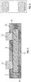
FIG. 1 is a cross sectional side view of a semiconductor package; -
FIG. 2 is a top view of a semiconductor package; -
FIG. 3 is a first process flow illustrating the formation of a semiconductor package; -
FIG. 4 is a top view of a semiconductor wafer with a plurality of notches cut therein; -
FIG. 5 is a top view of a semiconductor wafer with a plurality of notches etched therein; -
FIG. 6 is a top view of a second implementation of a semiconductor wafer with a plurality of notches etched therein; -
FIG. 7 is a top view of a third implementations of a semiconductor wafer with a plurality of notches etched therein; -
FIG. 8 is a cross sectional view of a portion of a wafer with molding applied thereto; -
FIG. 8A is a magnified cross sectional view of the bond between a mold and a sidewall of a notch formed in the die; -
FIG. 9 is a second process flow illustrating the formation of a semiconductor package; -
FIG. 10 is a third process flow illustrating a portion of the formation of a semiconductor package. -
FIG. 11 illustrates a first alternative for forming the notches in the third process flow. -
FIG. 12 illustrates a second alternative for forming the notches in the third process flow; -
FIG. 13 illustrates a third alternative for forming the notches in the third process flow; -
FIG. 14 illustrates a fourth alternative for forming the notches in the third process flow; and -
FIG. 15 is a fourth process flow illustrating the formation of a semiconductor package. - This disclosure, its aspects and implementations, are not limited to the specific components, assembly procedures or method elements disclosed herein. Many additional components, assembly procedures and/or method elements known in the art consistent with the intended semiconductor package will become apparent for use with particular implementations from this disclosure. Accordingly, for example, although particular implementations are disclosed, such implementations and implementing components may comprise any shape, size, style, type, model, version, measurement, concentration, material, quantity, method element, step, and/or the like as is known in the art for such semiconductor packages, and implementing components and methods, consistent with the intended operation and methods.
- Referring to
FIG. 1 , a cross sectional side view of a semiconductor package is illustrated. The semiconductor package includes a die 2 which includes a first side 4, asecond side 6, athird side 8 opposite thesecond side 6, a fourth side, a fifth side opposite the fourth side (both fourth and fifth sides are located into and out of the drawing surface in this view), and asixth side 10 opposite the first side 4. In various implementations, thesecond side 6 of the die 2, thethird side 8 of the die, the fourth side of the die, and/or the fifth side of the die may include a notch therein. - In various implementations, one or more
electrical contacts 12 are coupled to the first side 4 of the die 2. In various implementations, the electrical contacts are metal and may be, by non-limiting example, copper, silver, gold, nickel, titanium, aluminum, any combination or alloy thereof, or another metal. In still other implementations, theelectrical contacts 12 may not be metallic but may rather be another electrically conductive material. - In various implementations, a
first mold compound 14 covers the first, second, third, fourth, and fifth sides of the die. In various implementations, the mold compound may be, by non-limiting example, an epoxy mold compound, an acrylic molding compound, or another type of material capable of physically supporting the die and providing protection against ingress of contaminants. In various implementations, a laminate resin or second mold compound covers thesixth side 10 of the die. - The
electrical contacts 12 each extend through a corresponding plurality of openings in thefirst mold compound 14. In various implementations, theelectrical contacts 12 extend beyond the surface of themolding 14, as illustrated inFIG. 1 , while in other implementations the electrical contacts are level or flush with the surface of themolding compound 14. - In various implementations, the sides of the die will have no chips or cracks, particularly on the semiconductor device side of the die. This is accomplished through forming the second, third, fourth, and fifth sides of each die using etching techniques rather than a conventional sawing technique. Such a method is more fully disclosed is association with the discussion of
FIG. 3 herein. - Further, the first mold compound may be anchored to the second, third, fourth, and fifth sides of the die. In various implementations, the anchor effect is the result of interaction of the mold compound with a plurality of ridges formed along the second, third, fourth, and fifth sides of the die. This anchoring effect is more fully disclose in association with the discussion of
FIG. 3 herein. - Referring to
FIG. 2 , a top view of a semiconductor package is illustrated. Themolding compound 14 is clearly seen inFIG. 2 encompassing a perimeter of each electrical contact 12 (the shaded areas inFIG. 2 ) so that the entire first side of the die (along with every other side) is not exposed. - Referring to
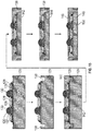
FIG. 3 , a first process flow illustrating the formation of a semiconductor package is illustrated. In various implementations, the method for making a semiconductor package includes providing awafer 16 which may include any particular type of substrate material, including, by non-limiting example, silicon, sapphire, ruby, gallium arsenide, glass, or any other semiconductor wafer substrate type. In various implementations, ametal layer 18 is formed on afirst side 28 of thewafer 16 and may be formed using a sputtering technique. In other implementations, themetal layer 18 is formed using other techniques, such as, by non-limiting example, electroplating, electroless plating, chemical vapor deposition, and other methods of depositing a metal layer. In a particular implementation, the metal layer is a titanium/copper seed layer, while in other implementations, the metal layer may include, by non-limiting example, copper, titanium, gold, nickel, aluminum, silver, or any combination or alloy thereof. - In various implementations, a
first photoresist layer 20 is formed and patterned over themetal layer 18. One or moreelectrical contacts 22 may be formed on themetal layer 18 and within thephotoresist layer 20. In various implementations this may be done using various electroplating or electroless plating techniques, though deposition and etching techniques could be employed in various implementations. Theelectrical contacts 22 may be any type of electrical contact previously disclosed herein (bumps, studs, and so forth). In various implementations, thefirst photoresist layer 20 is removed through an ashing or solvent dissolution process and themetal layer 18 may be etched away after the electrical contacts are formed. - In various implementations, a
second photoresist layer 24 is formed and patterned over thewafer 16. In various implementations, as illustrated inFIG. 3 , the secondpatterned photoresist layer 24 does not cover theelectrical contacts 22. In other implementations, the second photoresist layer is formed conformally over the electrical contacts along with the wafer. Referring toFIG. 9 , a second process flow illustrating the formation of a semiconductor package is illustrated. In this process flow, asecond photoresist layer 68 is formed as a conformal layer over theelectrical contacts 70. Aside from this difference, the process depicted inFIG. 9 includes the same process steps as the process depicted inFIG. 3 . - Referring back to
FIG. 3 , in various implementations, the method includes etching a plurality ofnotches 26 into thefirst side 28 of thewafer 16 using the second patterned photoresist layer. In various implementations, the width of the notches may be between about 50 and about 150 microns wide while in other implementations, the width of the notches may be less than about 50 microns or more than about 150 microns. In various implementations, the depth of the plurality ofnotches 26 may extend between about 25 and 200 microns into the wafer while in other implementations, the depth of the plurality ofnotches 26 may be less than about 25 microns or more than about 200 microns. - In various implementations, the plurality of notches may be formed using, by non-limiting example, plasma etching, deep-reactive ion etching, or wet chemical etching. In various implementations, a process marketed under the tradename BOSCH® by Robert Bosch GmbH, Stuttgart Germany (the "Bosch process"), may be used to form the plurality of
notches 26 in thefirst side 28 of thewafer 16. - Referring now to
FIG. 4 , a top view of a conventional semiconductor wafer with a plurality of saw cuts surrounding the plurality of die is illustrated. Using a saw to cut notches in a semiconductor wafer invariably results in the production of chips and cracks on the device side of the die and in thesidewalls 34 of thenotches 30. The presence of the cracks and chips has the potential to compromise the reliability of the semiconductor package if the cracks and chips propagate into the device portion of the semiconductor die. Since the saw process involves the rubbing of the rotating blade against the die surface, the chipping and cracking can only be managed through saw processing variables (wafer feed speed, blade kerf width, cut depth, multiple saw cuts, blade materials, etc.) but not eliminated. Furthermore, because the saw process relies on passing the wafer underneath the blades, only square and rectangular sized die are typically produced using conventional saw techniques. - Referring to
FIG. 5 , a top view of a semiconductor wafer with a plurality of notches etched therein is illustrated. In contrast to the appearance of the die processed using the conventional sawing method illustrated inFIG. 4 , the plurality ofnotches 36 in thewafer 38 formed using etching techniques have edges and sidewalls 40 that do not exhibit cracks or chips therein. Because of the absence of the cracks and chips, the use of etching techniques to form a plurality of notches in a semiconductor wafer is likely to improve the reliability of the resulting semiconductor packages. - Furthermore, using etching techniques to form a plurality of notches in a wafer allows for different shapes of perimeters of die to be produced. In various implementations, the second photoresist layer described in relation to
FIG. 3 may be patterned in a way to form a plurality of notches that do not form die with rectangular perimeters. For example, referring toFIG. 6 , a top view of a second implementation of a semiconductor wafer with a plurality of notches etched therein is illustrated. In various implementations, a plurality ofnotches 42 may be formed in a wafer 44. The plurality ofnotches 42 may form eventual die 46 with perimeters that are octagons. Referring toFIG. 7 , a top view of a third implementations of a semiconductor wafer with a plurality of notches etched therein is illustrated. In various implementations, a plurality ofnotches 48 may be formed in awafer 50. The plurality ofnotches 48 may form eventual die 52 with perimeters that are rounded rectangles. In other implementations, a plurality of notches may be formed in a wafer that form eventual die with perimeters that are any other closed geometrical shape. - Referring back to
FIG. 3 , in various implementations, the plurality ofnotches 26 formed have two substantially parallel sidewalls that extend substantially straight into thefirst side 28 of thewafer 16. In other implementations, two or more stepwise notches are formed in thefirst side 28 of thewafer 16. Each stepwise notch may be formed by creating a first notch in the wafer, and then forming a second more narrow notch within each first notch. - Referring to
FIG. 3 , an implementation of a method for forming a semiconductor package includes applying afirst mold compound 54 into the plurality ofnotches 26 and over the first side of the wafer. In various implementations, as illustrated byFIG. 3 , thefirst mold compound 54 may cover theelectrical contacts 22. In other implementations, thefirst mold compound 54 may not completely cover theelectrical contacts 22. The first mold compound may be applied using, by non-limiting example, a liquid dispensing technique, a transfer molding technique, a printer molding technique, or a compression molding technique. The molding compound may be an epoxy molding compound, an acrylic molding compound, or another type of molding compound disclosed herein. - In various implementations, the
first mold compound 54 may be anchored to a plurality ofsidewalls 56 of a plurality ofnotches 26. Referring now toFIG. 8 , a cross sectional view of a portion of a wafer with molding applied thereto is illustrated. Referring now toFIG. 8A , a magnified cross sectional view of the bond between a mold and a sidewall of a notch formed in the die is illustrated. In various implementations, a plurality ofridges 58 may be formed in asidewall 56 of each notch within the plurality of notches. In a particular implementation, the height of each ridge extending from the sidewall is substantially 0.2 microns tall with a pitch of substantially one micron. Thus, in implementations where the notch is 150 microns deep, there may be substantially 150 microns on each sidewall of the notch. In other implementations, the notches may be taller or shorter than 0.2 microns and may have a pitch more or less than one micron. The ridges may anchor thefirst mold compound 54 to thesidewalls 56 of the plurality of notches. In various implementations where the plurality of notches are etched using the Bosch process, the etching process may form ridges in the plurality of notches while etching the plurality of notches via the deposition/etching cycles of the deep reactive ion etch, thus increasing the adhesion between the first mold compound and the sidewall of each notch. - Referring back to
FIG. 3 , in various implementations where thefirst mold compound 54 covers theelectrical contacts 22, theelectrical contacts 22 may be exposed by grinding the first mold compound. In various implementations, asecond side 60 of thewafer 16 may be ground to the plurality ofnotches 26 formed in thefirst side 28 of thewafer 16. In this way the various die of the semiconductor wafer are singulated from each other. In various implementations, thesecond side 60 of thewafer 16 may be ground using, by non-limiting example, a mechanical polishing technique, a chemical etching technique, a combination of a mechanical polishing and chemical etching technique, or any other grinding technique. - In various implementations, a
second mold compound 62 or a laminate resin may be applied to thesecond side 60 of thewafer 16. In implementations where a second mold compound is applied, the mold compound may be any type of mold compound disclosed herein and may be applied using any technique disclosed herein. - In various implementations, as illustrated in the process flow depicted in
FIG. 3 , thefirst mold compound 54 is ground to expose theelectrical contacts 22 before thesecond side 60 of thewafer 16 is ground and the second mold compound is applied. In other implementations, thefirst mold compound 54 may be ground to expose theelectrical contacts 22 after thesecond side 60 of thewafer 16 is ground and the second mold compound is applied. - The method for making a semiconductor package includes singulating the
wafer 16 into a plurality of semiconductor packages 64. Thewafer 16 may be singulated by cutting or etching through the wafer where the plurality ofnotches 26 were originally formed. The wafer may be singulated by using, by non-limiting example, a saw, a laser, a waterjet, plasma etching, deep reactive-ion etching, or chemical etching. In various implementations, the Bosch process may be used to singulate thewafer 16. The method used to singulate the wafer may include singulating the wafer using thinner cuts or etches than were used to form the plurality ofnotches 26. In this manner, the first mold compound will cover the sides of each singulated die 66 within eachsemiconductor package 64. Specifically, in particular implementations the saw width used to singulate each semiconductor package may be between 20 and 40 microns thick. The semiconductor die within the semiconductor package may be covered by either a mold compound or a laminate resin on all six sides of the semiconductor die. - In various implementations, the first side of the die within each semiconductor package may include a perimeter that is, by non-limiting example, a rectangle, an octagon, a rectangle with rounded edges, or any other closed geometric shape.
- Referring now to
FIG. 10 , a third process flow illustrating a portion of the formation of a semiconductor package is illustrated. In various implementations the method for forming a semiconductor package includes providing awafer 72, which may be any type of wafer substrate disclosed herein. In various implementations, one ormore metal pads 74 may be coupled to afirst side 76 of thewafer 72. The metal pad may include, by non-limiting example, aluminum, copper, nickel silver, gold, titanium, or any combination or alloy thereof. - In various implementations, a
first passivation layer 78 may be coupled to a portion of thefirst side 76 of thewafer 72. Thefirst passivation layer 78 may be a silicon dioxide passivation layer in various implementations, though it could be any of a wide variety of other types of layers, including, by non-limiting example, silicon nitride, polyimide, or another polymer or deposited material. In various implementations, asecond passivation layer 80 may be coupled to a portion of thefirst side 76 of thewafer 72. Thesecond passivation layer 80 may be a silicon nitride passivation layer. The second passivation layer may include the same material or a different material from the first passivation layer. - In various implementations, a
third layer 82 may be coupled to a portion of thefirst side 76 of thewafer 72. The third layer may be either a polyimide, a polybenzoxazole, a phenol resin, or a combination of a polyimide, a polybenzoxazole, and a phenol resin. In various implementations, ametal seed layer 84 may be formed over the third layer and over thefirst side 76 of thewafer 72. Themetal seed layer 84 may be any type of metal layer disclosed herein. In various implementations, themetal seed layer 84 may directly contact portions of thefirst side 76 of thewafer 72. In various implementations, the method includes forming and patterning afirst photoresist layer 86 over themetal seed layer 84. - In various implementations, the method includes forming
electrical contacts 88 coupled to themetal seed layer 84 and within thefirst photoresist layer 86. Theelectrical contacts 88 may be any type of electrical contact disclosed herein. In various implementations, theelectrical contacts 88 may include afirst layer 90 and asecond layer 92. In various implementations, thefirst layer 90 may include copper and thesecond layer 92 may include tin, silver, or a combination of tin and silver. In various implementations, the method of forming a semiconductor package includes removing thefirst photoresist layer 86 and etching the portions of themetal seed layer 84 away that are not covered by the electrical contacts, after the electrical contacts are formed. - In various implementations, the method of forming a semiconductor package includes forming and patterning a
second photoresist layer 94 over thefirst side 76 of thewafer 72. In various implementations, the second photoresist layer covers theelectrical contacts 88, while in other implementations, thesecond photoresist layer 94 does not cover theelectrical contacts 88. Thesecond photoresist layer 94 may be used to etch a plurality ofnotches 96 into thewafer 72. The method includes removing thesecond photoresist layer 94 after the plurality of notches are etched into the wafer. - A first mold compound may be applied into the plurality of notches and over the
first side 76 of thewafer 72 in the same manner the first mold compound inFIG. 3 is applied. The remainder of the method for forming a semiconductor package as depicted inFIG. 10 may include exposing the electrical contacts through grinding, grinding the backside of the wafer to the plurality of notches, applying a second mold compound or laminate resin to a backside of the wafer, and singulating the wafer into a plurality of semiconductor packages. These portions of forming a semiconductor package may be the same as or similar to respective portions for forming a semiconductor package illustrated byFIG. 3 and previously disclosed herein. - In various implementations, the semiconductor package produced by the method depicted in
FIG. 10 may include one or more metal pads, one or more passivation layers, a polyimide, a phenol resin, a polybenzoxazole, and any combination thereof, between the semiconductor die and the first mold compound. - Referring to
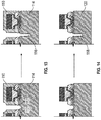
FIGS. 11-14 , alternative methods for forming a plurality of notches in the process illustrated byFIG. 10 is illustrated. Referring toFIG. 11 , a method of forming a plurality of notches using a patterned photoresist layer and one of a polyimide, polybenzoxazole, and a phenol resin in combination with an etching process is illustrated. In various implementations, a patternedphotoresist layer 98 may be over amask 100 including either a patterned polyimide layer, a patterned polybenzoxazole layer, or a patterned phenol resin layer. Themask 100 may be over awafer 102. Anotch 104 may be formed in thewafer 102 using the patterned photoresist layer and the mask using any etching process disclosed herein. - Referring to
FIG. 12 , a method of forming a plurality of notches using one of a polyimide, polybenzoxazole, and a phenol resin in combination with any etching process disclosed herein is illustrated. The method may be the same as the method depicted byFIG. 11 , with the difference being that the method depicted byFIG. 12 does not include a patterned photoresist layer used to form anotch 106 into awafer 108. - Referring to
FIG. 13 , a method of forming a plurality of notches using a patterned photoresist layer and passivation mask is illustrated. In various implementations, a patternedphotoresist layer 110 may be over apassivation mask 112. Thepassivation mask 112 may include any passivation layer disclosed herein. Thepassivation mask 112 may be over awafer 114. Anotch 116 may be formed in thewafer 114 using the patternedphotoresist layer 110 and thepassivation mask 112 and any etching process disclosed herein. - Referring to
FIG. 14 , a method of forming a plurality of notches using a passivation mask in combination with any of the etching method disclosed herein is illustrated. The method may be the same as the method depicted byFIG. 13 , with the difference being that the method depicted byFIG. 14 does not include a patterned photoresist layer used to form anotch 116 into awafer 118. - Referring to
FIG. 15 , a fourth process flow illustrating the formation of a semiconductor package is illustrated. The method for forming a semiconductor package illustrated inFIG. 15 includes providing awafer 120. In various implementations, aninterlayer 122 may be coupled to afirst side 124 of thewafer 120. In various implementations, apassivation layer 128 may be coupled to thewafer 120. The passivation layer may be any type of passivation layer disclosed herein. - In various implementations, one or more
electrical contacts 126 may be coupled to thewafer 120. In various implementations, the electrical contacts include abump 130. The electrical contacts may include afirst metal layer 132 coupled to thebump 130. The first metal layer may include any metal disclosed herein. In a particular implementation, the first metal layer includes nickel and gold. Theelectrical contacts 128 may include asecond metal layer 134 coupled to thefirst metal layer 132. Thesecond metal layer 134 may include any metal disclosed herein. In a particular implementation, thesecond metal layer 134 includes aluminum. In various implementations, a solder resistlayer 136 may be coupled over thewafer 120. In other implementations, no solder resist layer is included. - In various implementations, the
passivation layer 128 may be patterned and may directly contact portions of thewafer 120. In such implementations, the patterned passivation layer, or mask, may be used to etch a plurality ofnotches 138 into thefirst side 124 of thewafer 120 using any etching process disclosed herein. The plurality of notches may be etched using any method disclosed herein, and may be any type of notch previously disclosed herein. - In various implementations, a
first mold compound 140 is applied into the plurality ofnotches 138 and over thefirst wafer 120. Thefirst mold compound 140 may be any mold compound disclosed herein and may be applied using any technique disclosed herein. In various implementations, thefirst mold compound 140 does not entirely cover theelectrical contacts 126, as is illustrated byFIG. 15 . In other implementations, the first mold compound does entirely cover theelectrical contacts 126. In implementations where thefirst mold compound 140 does entirely cover theelectrical contacts 126, the first mold compound may be ground to expose theelectrical contacts 126. - In various implementations, a
second side 142 opposite thefirst side 124 of thewafer 120 may be ground using any grinding method disclosed herein to the plurality of notches. Asecond mold compound 144 or laminate resin may then be applied to thesecond side 142 of thewafer 120. - The
wafer 120 may then be singulated into a plurality of semiconductor packages 146. The wafer may be singulated using any technique disclosed herein. The semiconductor die 148 with thesemiconductor package 146 may have all six sides covered by a mold compound. In other implementations, the sixth side of thedie 150 may be covered by a laminate resin. - In various implementations, the semiconductor package formed by the method illustrated in
FIG. 15 may include either a solder resist layer, a passivation layer, an interlayer, or a combination of a solder resist layer, a passivation layer, and an interlayer coupled to the first side of the wafer and covered by the first mold compound. - Implementations of a method of forming a semiconductor package may include applying a first mold compound into the plurality of notches and over the first side of the wafer. The first mold compound may be applied using one of a printer molding technique and a compression molding technique.
- Implementations of a semiconductor package may include a die including a first side, a second side, a third side, a fourth side, a fifth side, and a sixth side, the first side of the die including a plurality of electrical contacts. The sixth side may oppose the first side.
- A perimeter of the first side of the die may include one of an octagon and a rounded rectangle.
- The plurality of electrical contacts may include one of a combination of nickel, gold, and aluminum and a combination of tin, silver, and copper.
- In places where the description above refers to particular implementations of semiconductor packages and implementing components, sub-components, methods and sub-methods, it should be readily apparent that a number of modifications may be made without departing from the spirit thereof and that these implementations, implementing components, sub-components, methods and sub-methods may be applied to other semiconductor packages.
Claims (15)
- A method of forming a semiconductor package comprising:forming a plurality of electrical contacts on a first side of a wafer;applying a photoresist layer to the first side of the wafer;patterning the photoresist layer;etching a plurality of notches into the first side of the wafer using the photoresist layer;applying a first mold compound into the plurality of notches and over the first side of the wafer;grinding a second side of the wafer opposite the first side of the wafer to the plurality of notches formed in the first side of the wafer;applying one of a second mold compound and a laminate resin to a second side of the wafer; andsingulating the wafer into a plurality of semiconductor packages, wherein six sides of each semiconductor package are covered by one of the first mold compound, the second mold compound, and the laminate resin.
- The method of claim 1, wherein a perimeter of a first side of a die within the package is substantially one of an octagon and a rectangle with rounded corners.
- The method of claim 1 or 2, wherein the plurality of notches are etched into the first side of the wafer using the photoresist layer and one of a polyimide, a polybenzoxazole, and a phenol resin.
- The method of claim 1 or 2, wherein the plurality of notches are etched into the first side of the wafer using the photoresist layer and a passivation mask.
- The method of any one of claims 1-4, wherein one of a solder resist layer, a passivation layer, an interlayer, and a combination of a solder resist layer, a passivation layer, and an interlayer is coupled to the first side of the wafer and covered by the first mold compound.
- A method of forming a semiconductor package comprising:forming a metal layer on a first side of a wafer;applying a first photoresist layer on the metal layer;patterning the first photoresist layer;forming electrical contacts coupled to the metal layer using the first photoresist layer;removing the first photoresist layer;etching the metal layer;etching a plurality of notches into the first side of the wafer;applying a first mold compound into the plurality of notches, over the electrical contacts, and over the first side of the wafer;exposing the electrical contacts through the first mold compound through grinding the first mold compound;grinding a second side of the wafer opposite the first side of the wafer to the plurality of notches formed in the first side of the wafer;applying one of a second mold compound and a laminate resin to the second side of the wafer;singulating the wafer into a plurality of semiconductor packages, wherein each semiconductor package is covered by one of a first molding compound, the second molding compound, and a laminate resin on the first side, the second side, a third side, a fourth side, a fifth side, and a sixth side of each semiconductor package.
- The method of claim 6, wherein a first side of a die within each semiconductor package comprises a perimeter that is one of an octagon and a rectangle with rounded edges.
- The method of claim 6 or 7, wherein the first mold compound is anchored to a sidewall of the plurality of notches through a plurality of ridges formed in the sidewall of the plurality of notches.
- The method of any one of claims 6-8, wherein the plurality of notches are formed using a deep reactive-ion etching technique during etching of the plurality of notches.
- The method of any one of claims 6-9, wherein the plurality of notches are etched into the first side of the wafer using one of a polyimide, a polybenzoxazole, and a phenol resin.
- The method of any one of claims 6-9, wherein the plurality of notches are etched into the first side of the wafer using a passivation mask.
- The method of any one of claims 6-11, wherein one of a solder resist layer, a passivation layer, an interlayer, and a combination of a solder resist layer, a passivation layer, and an interlayer is coupled to the first side of the wafer and covered by the first mold compound.
- A semiconductor package, comprising:a die comprising a first side, a second side, a third side, a fourth side, a fifth side, and a sixth side, the first side of the die comprising a plurality of electrical contacts;a first mold compound covering the first side of the die, the second side of the die, the third side of the die, the fourth side of the die, and the fifth side of the die, wherein the plurality of electrical contacts extend through a plurality of openings in the first mold compound; andone of a second mold compound and a laminate resin covering the sixth side of the die,wherein there is no die chipping of the first side of the die after singulation of the die.
- The package of claim 13, wherein the first mold compound is anchored to the second side of the die, the third side of the die, the fourth side of the die, and the fifth side of the die through a plurality of ridges formed in the second side of the die, the third side of the die, the fourth side of the die, and the fifth side of the die.
- The package of claim 13, further comprising one of a solder resist layer, a passivation layer, an interlayer, and a combination of a solder resist layer, a passivation layer, and an interlayer coupled to the first side of the wafer and covered by the first mold compound.
Applications Claiming Priority (1)
| Application Number | Priority Date | Filing Date | Title |
|---|---|---|---|
| US15/679,661 US10529576B2 (en) | 2017-08-17 | 2017-08-17 | Multi-faced molded semiconductor package and related methods |
Publications (2)
| Publication Number | Publication Date |
|---|---|
| EP3444838A1 true EP3444838A1 (en) | 2019-02-20 |
| EP3444838B1 EP3444838B1 (en) | 2023-08-30 |
Family
ID=62985945
Family Applications (1)
| Application Number | Title | Priority Date | Filing Date |
|---|---|---|---|
| EP18184165.1A Active EP3444838B1 (en) | 2017-08-17 | 2018-07-18 | Semiconductor package including a semiconductor die whose faces are all covered with molding material and related methods |
Country Status (3)
| Country | Link |
|---|---|
| US (4) | US10529576B2 (en) |
| EP (1) | EP3444838B1 (en) |
| CN (1) | CN109411368A (en) |
Families Citing this family (4)
| Publication number | Priority date | Publication date | Assignee | Title |
|---|---|---|---|---|
| CN110223924A (en) * | 2019-07-15 | 2019-09-10 | 珠海格力电器股份有限公司 | A kind of wafer level packaging method and wafer |
| US11121106B2 (en) * | 2019-10-31 | 2021-09-14 | Taiwan Semiconductor Manufacturing Company, Ltd. | Integrated circuit package and method |
| EP3852132A1 (en) * | 2020-01-20 | 2021-07-21 | Infineon Technologies Austria AG | Additive manufacturing of a frontside or backside interconnect of a semiconductor die |
| KR102813754B1 (en) * | 2021-01-26 | 2025-05-28 | 양쯔 메모리 테크놀로지스 씨오., 엘티디. | Substrate structure, its manufacturing and packaging method |
Citations (4)
| Publication number | Priority date | Publication date | Assignee | Title |
|---|---|---|---|---|
| US20110175242A1 (en) * | 2010-01-18 | 2011-07-21 | Grivna Gordon M | Method of forming a semiconductor die |
| US20140217556A1 (en) * | 2013-02-04 | 2014-08-07 | Avago Technologies General Ip (Singapore) Pte. Ltd. | Methods for dicing a compound semiconductor wafer, and diced wafers and die obtained thereby |
| CN104201114A (en) * | 2014-08-26 | 2014-12-10 | 江阴长电先进封装有限公司 | Packaging method and packaging structure of chip with sidewall in insulating protection |
| US20160225733A1 (en) * | 2013-11-26 | 2016-08-04 | Diodes Incorporation | Chip Scale Package |
Family Cites Families (20)
| Publication number | Priority date | Publication date | Assignee | Title |
|---|---|---|---|---|
| US6319796B1 (en) * | 1999-08-18 | 2001-11-20 | Vlsi Technology, Inc. | Manufacture of an integrated circuit isolation structure |
| JP4549366B2 (en) * | 2000-12-15 | 2010-09-22 | イビデン株式会社 | Multilayer printed wiring board |
| JP4761662B2 (en) * | 2001-07-17 | 2011-08-31 | 三洋電機株式会社 | Circuit device manufacturing method |
| JP3722784B2 (en) * | 2002-06-10 | 2005-11-30 | 松下電器産業株式会社 | Semiconductor device |
| KR20040006949A (en) * | 2002-07-16 | 2004-01-24 | 주식회사 하이닉스반도체 | Chip scale packaging method |
| US20070087544A1 (en) * | 2005-10-19 | 2007-04-19 | Taiwan Semiconductor Manufacturing Co., Ltd. | Method for forming improved bump structure |
| US7682874B2 (en) | 2006-07-10 | 2010-03-23 | Shanghai Kaihong Technology Co., Ltd. | Chip scale package (CSP) assembly apparatus and method |
| US7972521B2 (en) * | 2007-03-12 | 2011-07-05 | Semiconductor Components Industries Llc | Method of making reliable wafer level chip scale package semiconductor devices |
| CN101521165B (en) | 2008-02-26 | 2012-01-11 | 上海凯虹电子有限公司 | Chip-scale packaging method |
| CN101552248B (en) * | 2008-03-31 | 2013-01-23 | 兆装微股份有限公司 | A semiconductor device and a manufacturing method thereof |
| KR101067060B1 (en) * | 2009-06-18 | 2011-09-22 | 삼성전기주식회사 | Die package with encapsulated die and manufacturing method thereof |
| US8987878B2 (en) * | 2010-10-29 | 2015-03-24 | Alpha And Omega Semiconductor Incorporated | Substrateless power device packages |
| DE102013111503B4 (en) * | 2013-10-18 | 2021-08-05 | OSRAM Opto Semiconductors Gesellschaft mit beschränkter Haftung | Optoelectronic semiconductor chip, optoelectronic component and method for separating semiconductor chips |
| US9449943B2 (en) * | 2013-10-29 | 2016-09-20 | STATS ChipPAC Pte. Ltd. | Semiconductor device and method of balancing surfaces of an embedded PCB unit with a dummy copper pattern |
| US9679785B2 (en) | 2015-07-27 | 2017-06-13 | Semtech Corporation | Semiconductor device and method of encapsulating semiconductor die |
| US9899285B2 (en) | 2015-07-30 | 2018-02-20 | Semtech Corporation | Semiconductor device and method of forming small Z semiconductor package |
| US9496193B1 (en) | 2015-09-18 | 2016-11-15 | Infineon Technologies Ag | Semiconductor chip with structured sidewalls |
| US9646943B1 (en) * | 2015-12-31 | 2017-05-09 | Taiwan Semiconductor Manufacturing Company, Ltd. | Connector structure and method of forming same |
| JP6674677B2 (en) * | 2016-02-17 | 2020-04-01 | ローム株式会社 | Chip component and method of manufacturing the same |
| US10529671B2 (en) * | 2016-12-13 | 2020-01-07 | Taiwan Semiconductor Manufacturing Co., Ltd. | Package structure and method for forming the same |
-
2017
- 2017-08-17 US US15/679,661 patent/US10529576B2/en active Active
-
2018
- 2018-07-10 CN CN201810750840.8A patent/CN109411368A/en active Pending
- 2018-07-18 EP EP18184165.1A patent/EP3444838B1/en active Active
-
2019
- 2019-12-04 US US16/702,958 patent/US11328930B2/en active Active
-
2022
- 2022-04-05 US US17/658,071 patent/US12341014B2/en active Active
-
2025
- 2025-06-03 US US19/227,228 patent/US20250293032A1/en active Pending
Patent Citations (4)
| Publication number | Priority date | Publication date | Assignee | Title |
|---|---|---|---|---|
| US20110175242A1 (en) * | 2010-01-18 | 2011-07-21 | Grivna Gordon M | Method of forming a semiconductor die |
| US20140217556A1 (en) * | 2013-02-04 | 2014-08-07 | Avago Technologies General Ip (Singapore) Pte. Ltd. | Methods for dicing a compound semiconductor wafer, and diced wafers and die obtained thereby |
| US20160225733A1 (en) * | 2013-11-26 | 2016-08-04 | Diodes Incorporation | Chip Scale Package |
| CN104201114A (en) * | 2014-08-26 | 2014-12-10 | 江阴长电先进封装有限公司 | Packaging method and packaging structure of chip with sidewall in insulating protection |
Also Published As
| Publication number | Publication date |
|---|---|
| US10529576B2 (en) | 2020-01-07 |
| US20220230885A1 (en) | 2022-07-21 |
| US20200105536A1 (en) | 2020-04-02 |
| EP3444838B1 (en) | 2023-08-30 |
| US12341014B2 (en) | 2025-06-24 |
| CN109411368A (en) | 2019-03-01 |
| US11328930B2 (en) | 2022-05-10 |
| US20250293032A1 (en) | 2025-09-18 |
| US20190057874A1 (en) | 2019-02-21 |
Similar Documents
| Publication | Publication Date | Title |
|---|---|---|
| US12341014B2 (en) | Multi-faced molded semiconductor package and related methods | |
| US7838424B2 (en) | Enhanced reliability of wafer-level chip-scale packaging (WLCSP) die separation using dry etching | |
| US12040310B2 (en) | Methods of forming semiconductor packages with back side metal | |
| US20260026271A1 (en) | Semiconductor package electrical contacts and related methods | |
| US20260047368A1 (en) | Semiconductor package electrical contact structures and related methods | |
| US20160225733A1 (en) | Chip Scale Package | |
| US6887771B2 (en) | Semiconductor device and method for fabricating the same | |
| US20250149449A1 (en) | Thinned semiconductor package and related methods | |
| US20250232978A1 (en) | Semiconductor package stress balance structures and related methods | |
| US20200243389A1 (en) | Partial backside metal removal singulation system and related methods | |
| US20200258750A1 (en) | Die support structures and related methods | |
| CN107611096A (en) | Wafer stage chip encapsulating structure and preparation method thereof | |
| US20210118738A1 (en) | Semiconductor packages and methods of packaging semiconductor devices | |
| US11670549B2 (en) | Semiconductor packages without debris |
Legal Events
| Date | Code | Title | Description |
|---|---|---|---|
| PUAI | Public reference made under article 153(3) epc to a published international application that has entered the european phase |
Free format text: ORIGINAL CODE: 0009012 |
|
| STAA | Information on the status of an ep patent application or granted ep patent |
Free format text: STATUS: THE APPLICATION HAS BEEN PUBLISHED |
|
| AK | Designated contracting states |
Kind code of ref document: A1 Designated state(s): AL AT BE BG CH CY CZ DE DK EE ES FI FR GB GR HR HU IE IS IT LI LT LU LV MC MK MT NL NO PL PT RO RS SE SI SK SM TR |
|
| AX | Request for extension of the european patent |
Extension state: BA ME |
|
| STAA | Information on the status of an ep patent application or granted ep patent |
Free format text: STATUS: REQUEST FOR EXAMINATION WAS MADE |
|
| 17P | Request for examination filed |
Effective date: 20190624 |
|
| RBV | Designated contracting states (corrected) |
Designated state(s): AL AT BE BG CH CY CZ DE DK EE ES FI FR GB GR HR HU IE IS IT LI LT LU LV MC MK MT NL NO PL PT RO RS SE SI SK SM TR |
|
| STAA | Information on the status of an ep patent application or granted ep patent |
Free format text: STATUS: EXAMINATION IS IN PROGRESS |
|
| 17Q | First examination report despatched |
Effective date: 20210526 |
|
| GRAP | Despatch of communication of intention to grant a patent |
Free format text: ORIGINAL CODE: EPIDOSNIGR1 |
|
| STAA | Information on the status of an ep patent application or granted ep patent |
Free format text: STATUS: GRANT OF PATENT IS INTENDED |
|
| RIC1 | Information provided on ipc code assigned before grant |
Ipc: H01L 23/485 20060101ALI20230125BHEP Ipc: H01L 23/31 20060101ALI20230125BHEP Ipc: H01L 21/56 20060101ALI20230125BHEP Ipc: H01L 21/78 20060101AFI20230125BHEP |
|
| INTG | Intention to grant announced |
Effective date: 20230228 |
|
| GRAS | Grant fee paid |
Free format text: ORIGINAL CODE: EPIDOSNIGR3 |
|
| P01 | Opt-out of the competence of the unified patent court (upc) registered |
Effective date: 20230525 |
|
| GRAA | (expected) grant |
Free format text: ORIGINAL CODE: 0009210 |
|
| STAA | Information on the status of an ep patent application or granted ep patent |
Free format text: STATUS: THE PATENT HAS BEEN GRANTED |
|
| AK | Designated contracting states |
Kind code of ref document: B1 Designated state(s): AL AT BE BG CH CY CZ DE DK EE ES FI FR GB GR HR HU IE IS IT LI LT LU LV MC MK MT NL NO PL PT RO RS SE SI SK SM TR |
|
| REG | Reference to a national code |
Ref country code: GB Ref legal event code: FG4D |
|
| REG | Reference to a national code |
Ref country code: CH Ref legal event code: EP |
|
| REG | Reference to a national code |
Ref country code: DE Ref legal event code: R096 Ref document number: 602018056303 Country of ref document: DE |
|
| REG | Reference to a national code |
Ref country code: IE Ref legal event code: FG4D |
|
| REG | Reference to a national code |
Ref country code: LT Ref legal event code: MG9D |
|
| REG | Reference to a national code |
Ref country code: NL Ref legal event code: MP Effective date: 20230830 |
|
| REG | Reference to a national code |
Ref country code: AT Ref legal event code: MK05 Ref document number: 1606546 Country of ref document: AT Kind code of ref document: T Effective date: 20230830 |
|
| PG25 | Lapsed in a contracting state [announced via postgrant information from national office to epo] |
Ref country code: GR Free format text: LAPSE BECAUSE OF FAILURE TO SUBMIT A TRANSLATION OF THE DESCRIPTION OR TO PAY THE FEE WITHIN THE PRESCRIBED TIME-LIMIT Effective date: 20231201 |
|
| PG25 | Lapsed in a contracting state [announced via postgrant information from national office to epo] |
Ref country code: IS Free format text: LAPSE BECAUSE OF FAILURE TO SUBMIT A TRANSLATION OF THE DESCRIPTION OR TO PAY THE FEE WITHIN THE PRESCRIBED TIME-LIMIT Effective date: 20231230 |
|
| PG25 | Lapsed in a contracting state [announced via postgrant information from national office to epo] |
Ref country code: SE Free format text: LAPSE BECAUSE OF FAILURE TO SUBMIT A TRANSLATION OF THE DESCRIPTION OR TO PAY THE FEE WITHIN THE PRESCRIBED TIME-LIMIT Effective date: 20230830 Ref country code: RS Free format text: LAPSE BECAUSE OF FAILURE TO SUBMIT A TRANSLATION OF THE DESCRIPTION OR TO PAY THE FEE WITHIN THE PRESCRIBED TIME-LIMIT Effective date: 20230830 Ref country code: NO Free format text: LAPSE BECAUSE OF FAILURE TO SUBMIT A TRANSLATION OF THE DESCRIPTION OR TO PAY THE FEE WITHIN THE PRESCRIBED TIME-LIMIT Effective date: 20231130 Ref country code: LV Free format text: LAPSE BECAUSE OF FAILURE TO SUBMIT A TRANSLATION OF THE DESCRIPTION OR TO PAY THE FEE WITHIN THE PRESCRIBED TIME-LIMIT Effective date: 20230830 Ref country code: LT Free format text: LAPSE BECAUSE OF FAILURE TO SUBMIT A TRANSLATION OF THE DESCRIPTION OR TO PAY THE FEE WITHIN THE PRESCRIBED TIME-LIMIT Effective date: 20230830 Ref country code: IS Free format text: LAPSE BECAUSE OF FAILURE TO SUBMIT A TRANSLATION OF THE DESCRIPTION OR TO PAY THE FEE WITHIN THE PRESCRIBED TIME-LIMIT Effective date: 20231230 Ref country code: HR Free format text: LAPSE BECAUSE OF FAILURE TO SUBMIT A TRANSLATION OF THE DESCRIPTION OR TO PAY THE FEE WITHIN THE PRESCRIBED TIME-LIMIT Effective date: 20230830 Ref country code: GR Free format text: LAPSE BECAUSE OF FAILURE TO SUBMIT A TRANSLATION OF THE DESCRIPTION OR TO PAY THE FEE WITHIN THE PRESCRIBED TIME-LIMIT Effective date: 20231201 Ref country code: FI Free format text: LAPSE BECAUSE OF FAILURE TO SUBMIT A TRANSLATION OF THE DESCRIPTION OR TO PAY THE FEE WITHIN THE PRESCRIBED TIME-LIMIT Effective date: 20230830 Ref country code: AT Free format text: LAPSE BECAUSE OF FAILURE TO SUBMIT A TRANSLATION OF THE DESCRIPTION OR TO PAY THE FEE WITHIN THE PRESCRIBED TIME-LIMIT Effective date: 20230830 |
|
| PG25 | Lapsed in a contracting state [announced via postgrant information from national office to epo] |
Ref country code: PL Free format text: LAPSE BECAUSE OF FAILURE TO SUBMIT A TRANSLATION OF THE DESCRIPTION OR TO PAY THE FEE WITHIN THE PRESCRIBED TIME-LIMIT Effective date: 20230830 Ref country code: NL Free format text: LAPSE BECAUSE OF FAILURE TO SUBMIT A TRANSLATION OF THE DESCRIPTION OR TO PAY THE FEE WITHIN THE PRESCRIBED TIME-LIMIT Effective date: 20230830 |
|
| PG25 | Lapsed in a contracting state [announced via postgrant information from national office to epo] |
Ref country code: ES Free format text: LAPSE BECAUSE OF FAILURE TO SUBMIT A TRANSLATION OF THE DESCRIPTION OR TO PAY THE FEE WITHIN THE PRESCRIBED TIME-LIMIT Effective date: 20230830 |
|
| PG25 | Lapsed in a contracting state [announced via postgrant information from national office to epo] |
Ref country code: SM Free format text: LAPSE BECAUSE OF FAILURE TO SUBMIT A TRANSLATION OF THE DESCRIPTION OR TO PAY THE FEE WITHIN THE PRESCRIBED TIME-LIMIT Effective date: 20230830 Ref country code: RO Free format text: LAPSE BECAUSE OF FAILURE TO SUBMIT A TRANSLATION OF THE DESCRIPTION OR TO PAY THE FEE WITHIN THE PRESCRIBED TIME-LIMIT Effective date: 20230830 Ref country code: ES Free format text: LAPSE BECAUSE OF FAILURE TO SUBMIT A TRANSLATION OF THE DESCRIPTION OR TO PAY THE FEE WITHIN THE PRESCRIBED TIME-LIMIT Effective date: 20230830 Ref country code: EE Free format text: LAPSE BECAUSE OF FAILURE TO SUBMIT A TRANSLATION OF THE DESCRIPTION OR TO PAY THE FEE WITHIN THE PRESCRIBED TIME-LIMIT Effective date: 20230830 Ref country code: DK Free format text: LAPSE BECAUSE OF FAILURE TO SUBMIT A TRANSLATION OF THE DESCRIPTION OR TO PAY THE FEE WITHIN THE PRESCRIBED TIME-LIMIT Effective date: 20230830 Ref country code: CZ Free format text: LAPSE BECAUSE OF FAILURE TO SUBMIT A TRANSLATION OF THE DESCRIPTION OR TO PAY THE FEE WITHIN THE PRESCRIBED TIME-LIMIT Effective date: 20230830 Ref country code: SK Free format text: LAPSE BECAUSE OF FAILURE TO SUBMIT A TRANSLATION OF THE DESCRIPTION OR TO PAY THE FEE WITHIN THE PRESCRIBED TIME-LIMIT Effective date: 20230830 Ref country code: PT Free format text: LAPSE BECAUSE OF FAILURE TO SUBMIT A TRANSLATION OF THE DESCRIPTION OR TO PAY THE FEE WITHIN THE PRESCRIBED TIME-LIMIT Effective date: 20240102 |
|
| PG25 | Lapsed in a contracting state [announced via postgrant information from national office to epo] |
Ref country code: IT Free format text: LAPSE BECAUSE OF FAILURE TO SUBMIT A TRANSLATION OF THE DESCRIPTION OR TO PAY THE FEE WITHIN THE PRESCRIBED TIME-LIMIT Effective date: 20230830 |
|
| REG | Reference to a national code |
Ref country code: DE Ref legal event code: R097 Ref document number: 602018056303 Country of ref document: DE |
|
| PLBE | No opposition filed within time limit |
Free format text: ORIGINAL CODE: 0009261 |
|
| STAA | Information on the status of an ep patent application or granted ep patent |
Free format text: STATUS: NO OPPOSITION FILED WITHIN TIME LIMIT |
|
| PG25 | Lapsed in a contracting state [announced via postgrant information from national office to epo] |
Ref country code: SI Free format text: LAPSE BECAUSE OF FAILURE TO SUBMIT A TRANSLATION OF THE DESCRIPTION OR TO PAY THE FEE WITHIN THE PRESCRIBED TIME-LIMIT Effective date: 20230830 |
|
| 26N | No opposition filed |
Effective date: 20240603 |
|
| PG25 | Lapsed in a contracting state [announced via postgrant information from national office to epo] |
Ref country code: BG Free format text: LAPSE BECAUSE OF FAILURE TO SUBMIT A TRANSLATION OF THE DESCRIPTION OR TO PAY THE FEE WITHIN THE PRESCRIBED TIME-LIMIT Effective date: 20230830 |
|
| PG25 | Lapsed in a contracting state [announced via postgrant information from national office to epo] |
Ref country code: BG Free format text: LAPSE BECAUSE OF FAILURE TO SUBMIT A TRANSLATION OF THE DESCRIPTION OR TO PAY THE FEE WITHIN THE PRESCRIBED TIME-LIMIT Effective date: 20230830 |
|
| PG25 | Lapsed in a contracting state [announced via postgrant information from national office to epo] |
Ref country code: MC Free format text: LAPSE BECAUSE OF FAILURE TO SUBMIT A TRANSLATION OF THE DESCRIPTION OR TO PAY THE FEE WITHIN THE PRESCRIBED TIME-LIMIT Effective date: 20230830 |
|
| REG | Reference to a national code |
Ref country code: CH Ref legal event code: PL |
|
| PG25 | Lapsed in a contracting state [announced via postgrant information from national office to epo] |
Ref country code: LU Free format text: LAPSE BECAUSE OF NON-PAYMENT OF DUE FEES Effective date: 20240718 |
|
| GBPC | Gb: european patent ceased through non-payment of renewal fee |
Effective date: 20240718 |
|
| PG25 | Lapsed in a contracting state [announced via postgrant information from national office to epo] |
Ref country code: LU Free format text: LAPSE BECAUSE OF NON-PAYMENT OF DUE FEES Effective date: 20240718 |
|
| PG25 | Lapsed in a contracting state [announced via postgrant information from national office to epo] |
Ref country code: CH Free format text: LAPSE BECAUSE OF NON-PAYMENT OF DUE FEES Effective date: 20240731 Ref country code: BE Free format text: LAPSE BECAUSE OF NON-PAYMENT OF DUE FEES Effective date: 20240731 |
|
| PG25 | Lapsed in a contracting state [announced via postgrant information from national office to epo] |
Ref country code: FR Free format text: LAPSE BECAUSE OF NON-PAYMENT OF DUE FEES Effective date: 20240731 |
|
| PG25 | Lapsed in a contracting state [announced via postgrant information from national office to epo] |
Ref country code: GB Free format text: LAPSE BECAUSE OF NON-PAYMENT OF DUE FEES Effective date: 20240718 |
|
| REG | Reference to a national code |
Ref country code: BE Ref legal event code: MM Effective date: 20240731 |
|
| PG25 | Lapsed in a contracting state [announced via postgrant information from national office to epo] |
Ref country code: IE Free format text: LAPSE BECAUSE OF NON-PAYMENT OF DUE FEES Effective date: 20240718 |
|
| PGFP | Annual fee paid to national office [announced via postgrant information from national office to epo] |
Ref country code: DE Payment date: 20250620 Year of fee payment: 8 |
|
| PG25 | Lapsed in a contracting state [announced via postgrant information from national office to epo] |
Ref country code: CY Free format text: LAPSE BECAUSE OF FAILURE TO SUBMIT A TRANSLATION OF THE DESCRIPTION OR TO PAY THE FEE WITHIN THE PRESCRIBED TIME-LIMIT; INVALID AB INITIO Effective date: 20180718 |
|
| REG | Reference to a national code |
Ref country code: DE Ref legal event code: R079 Ref document number: 602018056303 Country of ref document: DE Free format text: PREVIOUS MAIN CLASS: H01L0021780000 Ipc: H10P0058000000 |
|
| PG25 | Lapsed in a contracting state [announced via postgrant information from national office to epo] |
Ref country code: HU Free format text: LAPSE BECAUSE OF FAILURE TO SUBMIT A TRANSLATION OF THE DESCRIPTION OR TO PAY THE FEE WITHIN THE PRESCRIBED TIME-LIMIT; INVALID AB INITIO Effective date: 20180718 |