EP3442209A1 - Splitter device and arrangement - Google Patents
Splitter device and arrangement Download PDFInfo
- Publication number
- EP3442209A1 EP3442209A1 EP18198044.2A EP18198044A EP3442209A1 EP 3442209 A1 EP3442209 A1 EP 3442209A1 EP 18198044 A EP18198044 A EP 18198044A EP 3442209 A1 EP3442209 A1 EP 3442209A1
- Authority
- EP
- European Patent Office
- Prior art keywords
- port
- splitter device
- pass filter
- ports
- switching
- Prior art date
- Legal status (The legal status is an assumption and is not a legal conclusion. Google has not performed a legal analysis and makes no representation as to the accuracy of the status listed.)
- Granted
Links
- 230000011664 signaling Effects 0.000 claims abstract description 3
- 238000005259 measurement Methods 0.000 description 11
- 238000010586 diagram Methods 0.000 description 4
- 238000012360 testing method Methods 0.000 description 2
- 230000005540 biological transmission Effects 0.000 description 1
- 230000001419 dependent effect Effects 0.000 description 1
- 238000006073 displacement reaction Methods 0.000 description 1
- 230000000694 effects Effects 0.000 description 1
- 238000009413 insulation Methods 0.000 description 1
- 238000012986 modification Methods 0.000 description 1
- 230000004048 modification Effects 0.000 description 1
- 230000001681 protective effect Effects 0.000 description 1
- 210000002105 tongue Anatomy 0.000 description 1
- 238000011144 upstream manufacturing Methods 0.000 description 1
Images


Classifications
-
- H—ELECTRICITY
- H04—ELECTRIC COMMUNICATION TECHNIQUE
- H04M—TELEPHONIC COMMUNICATION
- H04M11/00—Telephonic communication systems specially adapted for combination with other electrical systems
- H04M11/06—Simultaneous speech and data transmission, e.g. telegraphic transmission over the same conductors
- H04M11/062—Simultaneous speech and data transmission, e.g. telegraphic transmission over the same conductors using different frequency bands for speech and other data
-
- H—ELECTRICITY
- H04—ELECTRIC COMMUNICATION TECHNIQUE
- H04Q—SELECTING
- H04Q1/00—Details of selecting apparatus or arrangements
- H04Q1/02—Constructional details
- H04Q1/14—Distribution frames
- H04Q1/146—Distribution frames with line protection means
Definitions
- the invention relates to a splitter device and an arrangement with a splitter device.
- Splitter devices have been known for a long time for transmitting XDSL and POTS (Plain Old Telephone Service) signals or ISDN (Integrated Services Digital Network) signals to the subscriber or dividing up the incoming signals from the subscriber into XDSL and POTS/ISDN signals which are then forwarded to a DSLAM and a PSTN network (Public Switched Telephone Network).
- XDSL and POTS Packet Old Telephone Service
- ISDN Integrated Services Digital Network
- a splitter device of this type is known from WO 01/97532 A2 , which can be inserted in cassette elements or connector elements instead of overvoltage protection devices in a distributor block.
- a distributor connection module for telecommunications and data technology is known from WO 2013/189616 A1 , comprising a housing, wherein electrical input and output contacts which are designed as wire connection contacts are arranged in the housing.
- the input and output contacts are preferably insulation displacement contacts.
- the input and output contacts are electrically and mechanically interconnected via interface contacts which are designed, for example, as double-spring contacts and as contact tongues.
- the input contacts are arranged in a base module and the output contacts are arranged in at least two sub-modules, wherein the submodules are removable from or connectable to each other independently of the base module.
- the interface contacts of the sub-modules can also be designed as printed circuit boards. Functional elements such as, for example, surge arresters are additionally arranged in the sub-modules.
- the invention is based on the technical problem of providing a splitter device which is flexibly adaptable to different conditions.
- a further technical problem is the provision of an arrangement with a splitter device of this type which allows the splitter device to be looped into an existing distributor device.
- the splitter device comprises a high-pass filter, a low-pass filter, at least one first port, at least one second port and at least one third port, wherein the high-pass filter is arranged between the first and third port and the low-pass filter is arranged between the second and third port.
- the first port serves for the connection to a DSLAM for XDSL signals.
- the second port serves for the connection to a PSTN for POTS or ISDN signals
- the third port serves for the connection of a subscriber.
- the splitter device has an overvoltage protection circuit and at least one first switching element on the first port and at least one second switching element on the third port, wherein either the high-pass filter or the overvoltage protection circuit is switchable between the first and the third port by means of the first and second switching element.
- the splitter device has at least one overvoltage protection circuit and also at least one first switching element on the first port and at least one second switching element on the third port, wherein the at least one overvoltage protection circuit is arranged between the first port and the first switching element and/or between the third port and the second switching element and/or between the second port and the low-pass filter, wherein the high-pass filter is situated between the first and third ports for signalling purposes in a first switching position of the first and second switching elements, and, in a second switching position, the first and second switching elements are connected to one another directly.
- the high-pass filter performs the overvoltage protection function, since it is quickly destroyed in the event of overvoltage and thus, for example, protects the DSLAM.
- the circuit is designed in such a way that at least one overvoltage protection apparatus is arranged permanently on the at least one port and thus protects the technology downstream thereof.
- the port on which the overvoltage protection circuit is present may be dependent on the specifications of the network operator; in particular this can take into consideration where the occurrence of overvoltages in the infrastructure is particularly high.
- the splitter device therefore has precisely one overvoltage protection circuit that is arranged between the first port and the first switching element.
- the DSLAM arranged on the first port is provided with permanent protection against overvoltage.
- the high-pass filter is switched between the first and the third port in addition to the overvoltage protection. Conversely, if, for example, no POTS/ISDN signal is required, the high-pass filter can be omitted and the connection between the DSLAM and the subscriber can be directly established, wherein the overvoltage protection device prevents damage to components due to overvoltage.
- the splitter device has precisely two overvoltage protection circuits, wherein the first overvoltage protection circuit is arranged between the second port and the low-pass filter and the second overvoltage protection circuit is arranged between the third port and the second switching element.
- this embodiment requires two overvoltage protection circuits, it has the advantage that the components within the splitter device are better protected. This is based on the insight that overvoltages frequently arise on the subscriber lines and the lines to the PSTN, whereas this is relatively improbable in the DSLAM. Therefore, the two overvoltage circuits in this circuit block the overvoltages effectively and protect both the splitter device itself and DSLAM on the first port.
- the splitter device preferably has at least two first, at least two second and at least two third ports so that the data transmission can be implemented via wire pairs.
- the splitter device has precisely two first, second and third ports.
- the first and second switching elements are designed as relays so that the respectively unused circuit parts are galvanically isolated.
- the splitter device has a control unit which controls the switching elements.
- a voltage supply for example in the form of a battery, is preferably assigned to said control unit.
- the energy can also be transmitted via the ports.
- control unit is designed in such a way that, on detecting a control signal, it switches the overvoltage protection circuit temporarily for a predefined time period or permanently between the first and third port.
- An ILTF or MELT (integrated line test function or metallic line testing) measurement can thus be carried out.
- an ILTF sequence is transmitted from the DSLAM via the first port and is picked up by the control unit.
- the high-pass filter is disconnected and the ILTF measurement can be carried out into the subscriber line.
- the control unit may, for example, be designed with a, preferably programmable, timer.
- the switchover may also be permanent, for example because the subscriber no longer requires the PSTN connection with the POTS/ISDN signals.
- control unit is designed in such a way that, on picking up a control signal in the embodiment with a permanently connected overvoltage protection circuit, it disconnects the high-pass filter temporarily for a predefined time period or permanently between the first and third port.
- an ILTF or MELT measurement can thus be carried out.
- an ILTF sequence is transmitted from the DSLAM via the first port and is picked up by the control unit.
- the high-pass filter is disconnected and the ILTF measurement can be carried out into the subscriber line.
- the control unit may, for example, be designed with a, preferably programmable, timer.
- the switchover may also be permanent, for example because the subscriber no longer requires the PSTN connection with the POTS/ISDN signals.
- At least one voltage or current sensor is disposed on the second port, wherein the control unit is designed in such a way that, if the voltage or current sensor detects no signal, the overvoltage protection circuit is switched between the first and the third port. This means that the high-pass filter can be disconnected whenever no POTS/ISDN signal is present.
- the overvoltage protection device is switched between the first and third port when the relays are in a rest position.
- the splitter device is designed as a plug or magazine which can then be inserted, for example, into disconnection point contacts of a distributor connection module.
- the splitter device is integrated into a distributor connection module.
- the splitter device is integrated into a sub-module of a distributor connection module, wherein the distributor connection module is formed by a base module and at least two sub-modules.
- the distributor connection module is formed by a base module and at least two sub-modules.
- a printed circuit board which accommodates the components of the splitter device and forms the interface contacts is preferably arranged in the sub-module.
- the first port is formed by the interface contact of the sub-module and the second and third ports are formed by the output contacts of the sub-module.
- One sub-module is preferably assigned to precisely one subscriber, so that the sub-module has four output contacts.
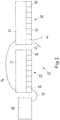
- Fig. 1 shows a splitter device 1 which has two first ports 11, two second ports 12 and two third ports 13. Furthermore, the splitter device 1 has a high-pass filter 2, a low-pass filter 3, an overvoltage protection circuit 4, a control unit 5 and a voltage sensor 6. Furthermore, two first switching elements 7 which are preferably designed as relays are arranged between the two first ports 11 and the high-pass filter 2 or the overvoltage protection circuit 4. Two second switching elements 8 are arranged between the high-pass filter 2 or the overvoltage protection circuit 4 and the two third ports 13. The two first switching elements 7 and the two switching elements 8 in each case have a first switch position and a second switch position, wherein the first switch position is shown by a continuous line and the second switch position by a dotted line.
- the high-pass filter 2 is located between the first ports 11 and the third ports 13 and, in the second switch position, the overvoltage protection circuit 4 is located between the first ports 11 and the third ports 13.
- the low-pass filter 3 is located between the second ports 12 and the second switching elements 8 and is connected to the high-pass filter 2.
- the voltage sensor 6 is located between the second ports 12 and the low-pass filter 3.
- the first and second switching elements 7, 8 are controlled by the control unit 5 which generates a control signal S for this purpose.
- the control unit 5 evaluates the signals V of the voltage sensor 6 and the signals between the first switching elements 7 and the high-pass filter 2 which are, for example, tapped with high impedance in order to influence the signal flow as little as possible.
- the first ports 11 are connected to an XDSL data source (e.g. a DSLAM).
- the second ports 12 are connected to a PSTN and the third ports 13 are connected to a subscriber.
- the splitter device 1 is explained below in its different modes of operation.
- the splitter device operates in the same way as a conventional splitter device and the high-frequency XDSL signals and the low-frequency POTS/ISDN signals are linked and transmitted to the subscriber.
- the incoming signals from the subscriber are divided up accordingly into XDSL signals and POTS/ISDN signals via the high-pass filter 2 or the low-pass filter 3.
- a separate overvoltage protection is dispensed with and said protection is provided via the high-pass filter 2 which is destroyed at an early stage if overvoltages occur, thereby interrupting the connection.
- the XDSL signal can be transmitted directly to the subscriber.
- the first switching elements 7 and the second switching elements 8 are switched into the second switch position, so that the overvoltage protection circuit 4 is located between the first ports 11 and the third ports 13.
- the absence of POTS/ISDN signals is detected by the voltage sensor 6 and is reported via the signal V to the control unit 5 which then generates the switching signals S.
- the first and second switching elements 7, 8 as relays, it can be provided that the field coils of the relays are arranged on the second ports 12 instead of the voltage sensor 6. If no POTS signal is then present, the relays drop out and switch to the second switch position.
- control unit 5 is instructed via an external command (for example from a higher-order management) to switch the first and second switch elements 7, 8 to the second switch position.
- an ILTF measurement is to be carried out with which the high-pass filter 2 would interfere.
- a corresponding DC sequence is transmitted via the first ports 11 and is picked up by the control unit 5 upstream of the high-pass filter 2.
- the control unit 5 then switches the first and second switching elements 7, 8 to the second switch position for the time of the subsequent measurement.
- the measurement period may, for example, be set via a timer in the control unit 5.
- a corresponding trigger e.g. from the ILTF or MELT measurement, can also be used, which is then evaluated by the control unit 5.
- the splitter device 1 can be integrated into a sub-module of a distributor connection module according to WO 2013/189616 A1 , wherein the wires for XDSL signals are then connected to the base module of the distributor connection module and are then tapped via the interface contacts of the sub-modules as first ports 11.
- the splitter device 1 can be looped into the existing cabling according to an arrangement 20 as shown in Fig. 2 .
- the arrangement comprises a first distributor connection module 30 and a second distributor connection module 40, wherein each distributor connection module 30, 40 comprises a base module 31, 41 and in each case eight sub-modules 32, 42.
- the XDSL signals are present on a distributor device 50.
- the XDSL signals are switched onto the sub-modules 32 of the first distributor connection module 30 by means of XDSL jumper wires 33, wherein only one XDSL jumper wire 33 is shown in Fig. 2 .
- the base modules 31, 41 of the two distributor connection modules 30, 40 are hardwired in advance by means of jumper wires 34, wherein again only one is shown by way of example.
- the splitter devices 1 according to Fig. 1 are then arranged in the sub-modules 42 of the second distributor connection module 40.
- the interface contact of the sub-module 42 forms the first ports 11, whereas the output contacts of the sub-module 42 designed as wire connection contacts form the second ports 12 and third ports 13 to which the POTS/ISDN wires 43 and subscriber lines 44 are then connected.
- the XDSL jumper wires 33, the jumper wires 34, the POTS/ISDN wires 43 and the subscriber lines 44 are preferably wire pairs, wherein one sub-module 42 is furthermore preferably assigned in each case to precisely one subscriber.
- Fig. 3 shows a splitter device 1 in an alternative embodiment which has two first ports 11, two second ports 12 and two third ports 13.
- the splitter device 1 furthermore has a high-pass filter 2, a low-pass filter 3, an overvoltage protection circuit 4, a control unit 5 and a voltage sensor 6.
- the overvoltage protection circuit 4 is furthermore arranged between the two first ports 11 and the two first switching elements 7.
- the two first switching elements 7 are arranged between the overvoltage protection circuit 4 and the high-pass filter 2 or two second switching elements 8 on the third ports 13.
- the first and second switching elements 7, 8 are preferably designed as relays.
- the two first switching elements 7 and the two switching elements 8 in each case have a first switch position and a second switch position, wherein the first switch position is shown by a continuous line and the second switch position by a dotted line.
- the overvoltage protection circuit 4 and the high-pass filter 2 are located between the first ports 11 and the third ports 13, and in the second switch position only the overvoltage protection circuit 4 is located between the first ports 11 and the third ports 13.
- the low-pass filter 3 is located between the second ports 12 and the second switching elements 8 and is connected to the high-pass filter 2.
- the voltage sensor 6 is located between the second ports 12 and the low-pass filter 3.
- the first and second switching elements 7, 8 are controlled by the control unit 5, which generates a control signal S for this purpose.
- the control unit 5 evaluates the signals V of the voltage sensor 6 and the signals between the first switching elements 7 and the high-pass filter 2 which, for example, are tapped with high impedance in order to influence the signal flow as little as possible.
- the first ports 11 are connected to an XDSL data source (e.g. a DSLAM) .
- the second ports 12 are connected to a PSTN and the third ports 13 to a subscriber.
- the splitter device 1 is explained below in its different modes of operation.
- the splitter device In the first switch position, the splitter device operates in the same way as a conventional splitter device and the high-frequency XDSL signals and the low-frequency POTS/ISDN signals are linked and transmitted to the subscriber.
- the incoming signals from the subscriber are divided up accordingly into XDSL signals and POTS/ISDN signals via the high-pass filter 2 or the low-pass filter 3.
- the overvoltage protection circuit 4 is switched between the first port and the high-pass filter 2 in order to further increase the protective effect against damage to the DSLAM by overvoltage events.
- the XDSL signal can be transmitted directly to the subscriber.
- the first switching elements 7 and the second switching elements 8 are switched into the second switch position, so that the overvoltage protection circuit 4 is located between the first ports 11 and the third ports 13.
- the absence of POTS/ISDN signals is detected by the voltage sensor 6 and is reported via the signal V to the control unit 5 which then generates the switching signals S.
- the first and second switching elements 7, 8 as relays, it can be provided that the field coils of the relays are arranged on the second ports 12 instead of the voltage sensor 6. If no POTS signal is then present, the relays drop out and switch to the second switch position.
- control unit 5 is instructed via an external command (for example from a higher-order management) to switch the first and second switch elements 7, 8 to the second switch position.
- Fig. 4 shows a further alternative embodiment for a splitter device 1.
- the splitter device 1 has two overvoltage protection circuits 4, wherein a first overvoltage protection circuit 4 is situated between the second ports 12 and the low-pass filter 3 or the voltage sensor 6 and a second overvoltage protection circuit 4 is situated between the third ports 13 and the second switching elements 8.
- the two overvoltage protection circuits 4 are permanently in effect and protect the splitter device 1 and also the xDSL data source on the first ports 11 against overvoltages from the subscriber lines or the POTS lines. Otherwise, reference can be made to the full content of the details described in relation to the Fig. 3 .
Abstract
Description
- The invention relates to a splitter device and an arrangement with a splitter device.
- Splitter devices have been known for a long time for transmitting XDSL and POTS (Plain Old Telephone Service) signals or ISDN (Integrated Services Digital Network) signals to the subscriber or dividing up the incoming signals from the subscriber into XDSL and POTS/ISDN signals which are then forwarded to a DSLAM and a PSTN network (Public Switched Telephone Network).
- A splitter device of this type is known from
WO 01/97532 A2 - A distributor connection module for telecommunications and data technology is known from
WO 2013/189616 A1 , comprising a housing, wherein electrical input and output contacts which are designed as wire connection contacts are arranged in the housing. The input and output contacts are preferably insulation displacement contacts. The input and output contacts are electrically and mechanically interconnected via interface contacts which are designed, for example, as double-spring contacts and as contact tongues. The input contacts are arranged in a base module and the output contacts are arranged in at least two sub-modules, wherein the submodules are removable from or connectable to each other independently of the base module. The interface contacts of the sub-modules can also be designed as printed circuit boards. Functional elements such as, for example, surge arresters are additionally arranged in the sub-modules. - The invention is based on the technical problem of providing a splitter device which is flexibly adaptable to different conditions. A further technical problem is the provision of an arrangement with a splitter device of this type which allows the splitter device to be looped into an existing distributor device.
- The technical problem is solved by a splitter device with the features of Claim 1 and an arrangement with the features of
Claim 13. Further advantageous designs of the invention can be found in the subclaims. - For this purpose, the splitter device comprises a high-pass filter, a low-pass filter, at least one first port, at least one second port and at least one third port, wherein the high-pass filter is arranged between the first and third port and the low-pass filter is arranged between the second and third port. The first port serves for the connection to a DSLAM for XDSL signals. The second port serves for the connection to a PSTN for POTS or ISDN signals, and the third port serves for the connection of a subscriber. The splitter device has an overvoltage protection circuit and at least one first switching element on the first port and at least one second switching element on the third port, wherein either the high-pass filter or the overvoltage protection circuit is switchable between the first and the third port by means of the first and second switching element. Alternatively, the splitter device has at least one overvoltage protection circuit and also at least one first switching element on the first port and at least one second switching element on the third port, wherein the at least one overvoltage protection circuit is arranged between the first port and the first switching element and/or between the third port and the second switching element and/or between the second port and the low-pass filter, wherein the high-pass filter is situated between the first and third ports for signalling purposes in a first switching position of the first and second switching elements, and, in a second switching position, the first and second switching elements are connected to one another directly.
- In normal operation, in the first alternative without a permanent overvoltage protection circuit, the high-pass filter performs the overvoltage protection function, since it is quickly destroyed in the event of overvoltage and thus, for example, protects the DSLAM.
- In the second alternative, the circuit is designed in such a way that at least one overvoltage protection apparatus is arranged permanently on the at least one port and thus protects the technology downstream thereof. In this case, the port on which the overvoltage protection circuit is present may be dependent on the specifications of the network operator; in particular this can take into consideration where the occurrence of overvoltages in the infrastructure is particularly high. There may also be a respective overvoltage protection circuit arranged on each of the three ports in this case. This requires a corresponding number of components, however.
- In one embodiment, the splitter device therefore has precisely one overvoltage protection circuit that is arranged between the first port and the first switching element. Thus the DSLAM arranged on the first port is provided with permanent protection against overvoltage. When a POTS/ISDN signal is present, the high-pass filter is switched between the first and the third port in addition to the overvoltage protection. Conversely, if, for example, no POTS/ISDN signal is required, the high-pass filter can be omitted and the connection between the DSLAM and the subscriber can be directly established, wherein the overvoltage protection device prevents damage to components due to overvoltage.
- In an alternative embodiment, the splitter device has precisely two overvoltage protection circuits, wherein the first overvoltage protection circuit is arranged between the second port and the low-pass filter and the second overvoltage protection circuit is arranged between the third port and the second switching element. Although this embodiment requires two overvoltage protection circuits, it has the advantage that the components within the splitter device are better protected. This is based on the insight that overvoltages frequently arise on the subscriber lines and the lines to the PSTN, whereas this is relatively improbable in the DSLAM. Therefore, the two overvoltage circuits in this circuit block the overvoltages effectively and protect both the splitter device itself and DSLAM on the first port.
- The splitter device preferably has at least two first, at least two second and at least two third ports so that the data transmission can be implemented via wire pairs. In one embodiment, the splitter device has precisely two first, second and third ports.
- In a further embodiment, the first and second switching elements are designed as relays so that the respectively unused circuit parts are galvanically isolated.
- In a further embodiment, the splitter device has a control unit which controls the switching elements. A voltage supply, for example in the form of a battery, is preferably assigned to said control unit. Alternatively, the energy can also be transmitted via the ports.
- In a further embodiment, the control unit is designed in such a way that, on detecting a control signal, it switches the overvoltage protection circuit temporarily for a predefined time period or permanently between the first and third port. An ILTF or MELT (integrated line test function or metallic line testing) measurement, for example, can thus be carried out. To do this, for example, an ILTF sequence is transmitted from the DSLAM via the first port and is picked up by the control unit. The high-pass filter is disconnected and the ILTF measurement can be carried out into the subscriber line. On completion of the measurement, the high-pass filter is then reconnected. To do this, the control unit may, for example, be designed with a, preferably programmable, timer. However, the switchover may also be permanent, for example because the subscriber no longer requires the PSTN connection with the POTS/ISDN signals.
- In a further embodiment, the control unit is designed in such a way that, on picking up a control signal in the embodiment with a permanently connected overvoltage protection circuit, it disconnects the high-pass filter temporarily for a predefined time period or permanently between the first and third port. For example, an ILTF or MELT measurement can thus be carried out. To do this, for example, an ILTF sequence is transmitted from the DSLAM via the first port and is picked up by the control unit. The high-pass filter is disconnected and the ILTF measurement can be carried out into the subscriber line. On completion of the measurement, the high-pass filter is then reconnected. To do this, the control unit may, for example, be designed with a, preferably programmable, timer. However, the switchover may also be permanent, for example because the subscriber no longer requires the PSTN connection with the POTS/ISDN signals.
- In a further embodiment, at least one voltage or current sensor is disposed on the second port, wherein the control unit is designed in such a way that, if the voltage or current sensor detects no signal, the overvoltage protection circuit is switched between the first and the third port. This means that the high-pass filter can be disconnected whenever no POTS/ISDN signal is present.
- In the case of the embodiments with a permanent overvoltage protection circuit or permanent overvoltage protection circuits, on the other hand, only the high-pass filter is disconnected from the signal path between the first and third ports.
- In a further embodiment, the overvoltage protection device is switched between the first and third port when the relays are in a rest position.
- In a further embodiment, the splitter device is designed as a plug or magazine which can then be inserted, for example, into disconnection point contacts of a distributor connection module. Alternatively, the splitter device is integrated into a distributor connection module.
- In a further embodiment, the splitter device is integrated into a sub-module of a distributor connection module, wherein the distributor connection module is formed by a base module and at least two sub-modules. In terms of the design of the base module and the sub-modules, reference is made to
WO 2013/189616 A1 . A printed circuit board which accommodates the components of the splitter device and forms the interface contacts is preferably arranged in the sub-module. - In a preferred embodiment, the first port is formed by the interface contact of the sub-module and the second and third ports are formed by the output contacts of the sub-module. The advantage is that the wiring of the XDSL lines is implemented on the base module, which normally requires no further modification.
- If wire pairs are used, four output contacts are then required for the wire pair to the subscriber and the wire pair to the PSTN. One sub-module is preferably assigned to precisely one subscriber, so that the sub-module has four output contacts.
- The invention is explained in detail below with reference to a preferred example embodiment. In the figures:
- Fig. 1
- shows a schematic block diagram of a splitter device in a first embodiment,
- Fig. 2
- shows a schematic block diagram of an arrangement with a splitter device,
- Fig. 3
- shows a schematic block diagram of a splitter device in a second embodiment, and
- Fig. 4
- shows a schematic block diagram of a splitter arrangement in a third embodiment.
-
Fig. 1 shows a splitter device 1 which has twofirst ports 11, twosecond ports 12 and twothird ports 13. Furthermore, the splitter device 1 has a high-pass filter 2, a low-pass filter 3, anovervoltage protection circuit 4, acontrol unit 5 and avoltage sensor 6. Furthermore, twofirst switching elements 7 which are preferably designed as relays are arranged between the twofirst ports 11 and the high-pass filter 2 or theovervoltage protection circuit 4. Twosecond switching elements 8 are arranged between the high-pass filter 2 or theovervoltage protection circuit 4 and the twothird ports 13. The twofirst switching elements 7 and the twoswitching elements 8 in each case have a first switch position and a second switch position, wherein the first switch position is shown by a continuous line and the second switch position by a dotted line. In the first switch position, the high-pass filter 2 is located between thefirst ports 11 and thethird ports 13 and, in the second switch position, theovervoltage protection circuit 4 is located between thefirst ports 11 and thethird ports 13. The low-pass filter 3 is located between thesecond ports 12 and thesecond switching elements 8 and is connected to the high-pass filter 2. Thevoltage sensor 6 is located between thesecond ports 12 and the low-pass filter 3. The first andsecond switching elements control unit 5 which generates a control signal S for this purpose. Thecontrol unit 5 evaluates the signals V of thevoltage sensor 6 and the signals between thefirst switching elements 7 and the high-pass filter 2 which are, for example, tapped with high impedance in order to influence the signal flow as little as possible. Thefirst ports 11 are connected to an XDSL data source (e.g. a DSLAM). Thesecond ports 12 are connected to a PSTN and thethird ports 13 are connected to a subscriber. - The splitter device 1 is explained below in its different modes of operation.
- In the first switch position, the splitter device operates in the same way as a conventional splitter device and the high-frequency XDSL signals and the low-frequency POTS/ISDN signals are linked and transmitted to the subscriber. The incoming signals from the subscriber are divided up accordingly into XDSL signals and POTS/ISDN signals via the high-
pass filter 2 or the low-pass filter 3. A separate overvoltage protection is dispensed with and said protection is provided via the high-pass filter 2 which is destroyed at an early stage if overvoltages occur, thereby interrupting the connection. - If no POTS/ISDN signals are present for whatever reason, the division of the signals via the high-
pass filter 2 and the low-pass filter 3 is not required. In this case, the XDSL signal can be transmitted directly to the subscriber. In this case, thefirst switching elements 7 and thesecond switching elements 8 are switched into the second switch position, so that theovervoltage protection circuit 4 is located between thefirst ports 11 and thethird ports 13. The absence of POTS/ISDN signals is detected by thevoltage sensor 6 and is reported via the signal V to thecontrol unit 5 which then generates the switching signals S. Alternatively, in one design of the first andsecond switching elements second ports 12 instead of thevoltage sensor 6. If no POTS signal is then present, the relays drop out and switch to the second switch position. - It can furthermore be provided that the
control unit 5 is instructed via an external command (for example from a higher-order management) to switch the first andsecond switch elements - It can furthermore be provided that an ILTF measurement is to be carried out with which the high-
pass filter 2 would interfere. For this purpose, a corresponding DC sequence is transmitted via thefirst ports 11 and is picked up by thecontrol unit 5 upstream of the high-pass filter 2. Thecontrol unit 5 then switches the first andsecond switching elements control unit 5. Alternatively to the DC sequence, a corresponding trigger, e.g. from the ILTF or MELT measurement, can also be used, which is then evaluated by thecontrol unit 5. - The splitter device 1 can be integrated into a sub-module of a distributor connection module according to
WO 2013/189616 A1 , wherein the wires for XDSL signals are then connected to the base module of the distributor connection module and are then tapped via the interface contacts of the sub-modules asfirst ports 11. - Conversely, if a cabling already exists, the splitter device 1 can be looped into the existing cabling according to an
arrangement 20 as shown inFig. 2 . - The arrangement comprises a first
distributor connection module 30 and a seconddistributor connection module 40, wherein eachdistributor connection module base module 31, 41 and in each case eight sub-modules 32, 42. The XDSL signals are present on adistributor device 50. The XDSL signals are switched onto the sub-modules 32 of the firstdistributor connection module 30 by means ofXDSL jumper wires 33, wherein only oneXDSL jumper wire 33 is shown inFig. 2 . Thebase modules 31, 41 of the twodistributor connection modules jumper wires 34, wherein again only one is shown by way of example. The splitter devices 1 according toFig. 1 are then arranged in thesub-modules 42 of the seconddistributor connection module 40. The interface contact of the sub-module 42 forms thefirst ports 11, whereas the output contacts of the sub-module 42 designed as wire connection contacts form thesecond ports 12 andthird ports 13 to which the POTS/ISDN wires 43 andsubscriber lines 44 are then connected. TheXDSL jumper wires 33, thejumper wires 34, the POTS/ISDN wires 43 and thesubscriber lines 44 are preferably wire pairs, wherein onesub-module 42 is furthermore preferably assigned in each case to precisely one subscriber. -
Fig. 3 shows a splitter device 1 in an alternative embodiment which has twofirst ports 11, twosecond ports 12 and twothird ports 13. The splitter device 1 furthermore has a high-pass filter 2, a low-pass filter 3, anovervoltage protection circuit 4, acontrol unit 5 and avoltage sensor 6. Theovervoltage protection circuit 4 is furthermore arranged between the twofirst ports 11 and the twofirst switching elements 7. The twofirst switching elements 7 are arranged between theovervoltage protection circuit 4 and the high-pass filter 2 or twosecond switching elements 8 on thethird ports 13. The first andsecond switching elements first switching elements 7 and the twoswitching elements 8 in each case have a first switch position and a second switch position, wherein the first switch position is shown by a continuous line and the second switch position by a dotted line. In the first switch position, theovervoltage protection circuit 4 and the high-pass filter 2 are located between thefirst ports 11 and thethird ports 13, and in the second switch position only theovervoltage protection circuit 4 is located between thefirst ports 11 and thethird ports 13. The low-pass filter 3 is located between thesecond ports 12 and thesecond switching elements 8 and is connected to the high-pass filter 2. Thevoltage sensor 6 is located between thesecond ports 12 and the low-pass filter 3. The first andsecond switching elements control unit 5, which generates a control signal S for this purpose. Thecontrol unit 5 evaluates the signals V of thevoltage sensor 6 and the signals between thefirst switching elements 7 and the high-pass filter 2 which, for example, are tapped with high impedance in order to influence the signal flow as little as possible. Thefirst ports 11 are connected to an XDSL data source (e.g. a DSLAM) . Thesecond ports 12 are connected to a PSTN and thethird ports 13 to a subscriber. - The splitter device 1 is explained below in its different modes of operation.
- In the first switch position, the splitter device operates in the same way as a conventional splitter device and the high-frequency XDSL signals and the low-frequency POTS/ISDN signals are linked and transmitted to the subscriber. The incoming signals from the subscriber are divided up accordingly into XDSL signals and POTS/ISDN signals via the high-
pass filter 2 or the low-pass filter 3. Although the high-pass filter 2 is destroyed at an early stage if overvoltages occur, thereby interrupting the connection, theovervoltage protection circuit 4 is switched between the first port and the high-pass filter 2 in order to further increase the protective effect against damage to the DSLAM by overvoltage events. - If no POTS/ISDN signals are present for whatever reason, the division of the signals via the high-
pass filter 2 and the low-pass filter 3 is not required. In this case, the XDSL signal can be transmitted directly to the subscriber. To do this, thefirst switching elements 7 and thesecond switching elements 8 are switched into the second switch position, so that theovervoltage protection circuit 4 is located between thefirst ports 11 and thethird ports 13. The absence of POTS/ISDN signals is detected by thevoltage sensor 6 and is reported via the signal V to thecontrol unit 5 which then generates the switching signals S. Alternatively, in one design of the first andsecond switching elements second ports 12 instead of thevoltage sensor 6. If no POTS signal is then present, the relays drop out and switch to the second switch position. - It can furthermore be provided that the
control unit 5 is instructed via an external command (for example from a higher-order management) to switch the first andsecond switch elements - In terms of the switchover on the basis of ILTF or MELT measurements, reference can be made to the details described in relation to
Fig. 1 . -
Fig. 4 shows a further alternative embodiment for a splitter device 1. In contrast to the embodiment shown inFig. 3 , the splitter device 1 has twoovervoltage protection circuits 4, wherein a firstovervoltage protection circuit 4 is situated between thesecond ports 12 and the low-pass filter 3 or thevoltage sensor 6 and a secondovervoltage protection circuit 4 is situated between thethird ports 13 and thesecond switching elements 8. The twoovervoltage protection circuits 4 are permanently in effect and protect the splitter device 1 and also the xDSL data source on thefirst ports 11 against overvoltages from the subscriber lines or the POTS lines. Otherwise, reference can be made to the full content of the details described in relation to theFig. 3 .
Claims (9)
- Splitter device (1) for telecommunications and data technology, comprising a high-pass filter (2), a low-pass filter (3), at least one first port (11), at least one second port (12) and at least one third port (13), wherein the high-pass filter (2) is arranged between the first port (11) and the third port (13) and the low-pass filter (3) is arranged between the second port (12) and the third port (13), wherein
the splitter device (1) has at least one first switching element (7) on the first port (11) and at least one further switching element (8) on the third port (13),the splitter device (1) has at least one overvoltage protection circuit (4), wherein the at least one overvoltage protection circuit (4) is arranged between the third port (13) and the second switching element (8) and/or between the second port (12) and the low- pass filter (3), wherein the high-pass filter (2) is situated between the first and third ports (11,13) for signaling purposes in a first switching position of the first and second switching elements (7, 8) and, in a second switching position, the first and second switching elements (7, 8) are connected to one another directly,
characterized in that
the splitter device (1) has a control unit (5) which controls the switching elements (7, 8) wherein the control unit (5) is designed in such a way that on picking up a DC sequence or a corresponding trigger signal over the first port (11) to switch the switching elements (7, 8) temporarily for a predefined time period or permanently from the first switching position to the second switching position and/or at least a voltage or current sensor (6) is disposed on the second port (12), wherein the control unit (5) is designed in such a way that, if the voltage or current sensor (6) detects no signal (V), the switching elements (7, 8) are switched from the first switching position to the second switching position. - Splitter device according to Claim 1, characterized in that the splitter device (1) has precisely two overvoltage protection circuits (4), wherein the first overvoltage protection circuit (4) is arranged between the second port (12) and the low-pass filter (3) and the second overvoltage protection circuit (4) is arranged between the third port (13) and the second switching element (8).
- Splitter device according to one of the preceding claims, characterized in that the splitter device (1) has at least two first ports (11), at least two second ports (12) and at least two third ports (13), wherein two of the ports (11, 12, 13) are in each case assigned to a subscriber.
- Splitter device according to one of the preceding claims, characterized in that the first and second switching elements (7, 8) are designed as relays.
- Splitter device according to Claim 4, characterized in that the overvoltage protection device (4) is switched between the first port (11) and the third port (13) when the relays are in a rest position.
- Splitter device according to one of the preceding claims, characterized in that the splitter device (1) is designed as a plug or magazine or is integrated into a distributor connection module (40).
- Splitter device according to Claim 6, characterized in that the splitter device (1) is integrated into a sub-module (42) of a distributor connection module (40), wherein the distributor connection module (40) is formed by a base module (41) and at least two sub-modules (42).
- Splitter device according to Claim 7, characterized in that the first port (11) is formed by the interface contacts of the sub-module (42) and the second and third port (12, 13) are formed by the output contacts of the sub-module (42).
- Arrangement (20) with a splitter device (1) as claimed in one of Claims 6 to 8, comprising at least one first distributor connection module (30) and one second distributor connection module (40), wherein each distributor connection module (30, 40) comprises a base module (31, 41) and at least two sub-modules (32, 42), wherein the two base modules (31, 41) are electrically connected via jumper wires (34), wherein XDSL jumper wires (33) are connected to the sub-modules (32) of the first distributor connection module (30) and the splitter devices (1) are integrated into the sub- modules (42) of the second distributor connection module (40).
Applications Claiming Priority (2)
| Application Number | Priority Date | Filing Date | Title |
|---|---|---|---|
| DE102015223222.0A DE102015223222A1 (en) | 2015-11-24 | 2015-11-24 | Splitter device and arrangement |
| EP16199061.9A EP3174272B1 (en) | 2015-11-24 | 2016-11-16 | Splitter device and arrangement |
Related Parent Applications (2)
| Application Number | Title | Priority Date | Filing Date |
|---|---|---|---|
| EP16199061.9A Division EP3174272B1 (en) | 2015-11-24 | 2016-11-16 | Splitter device and arrangement |
| EP16199061.9A Division-Into EP3174272B1 (en) | 2015-11-24 | 2016-11-16 | Splitter device and arrangement |
Publications (2)
| Publication Number | Publication Date |
|---|---|
| EP3442209A1 true EP3442209A1 (en) | 2019-02-13 |
| EP3442209B1 EP3442209B1 (en) | 2020-03-18 |
Family
ID=57482145
Family Applications (2)
| Application Number | Title | Priority Date | Filing Date |
|---|---|---|---|
| EP16199061.9A Not-in-force EP3174272B1 (en) | 2015-11-24 | 2016-11-16 | Splitter device and arrangement |
| EP18198044.2A Active EP3442209B1 (en) | 2015-11-24 | 2016-11-16 | Splitter device and arrangement |
Family Applications Before (1)
| Application Number | Title | Priority Date | Filing Date |
|---|---|---|---|
| EP16199061.9A Not-in-force EP3174272B1 (en) | 2015-11-24 | 2016-11-16 | Splitter device and arrangement |
Country Status (2)
| Country | Link |
|---|---|
| EP (2) | EP3174272B1 (en) |
| DE (1) | DE102015223222A1 (en) |
Citations (5)
| Publication number | Priority date | Publication date | Assignee | Title |
|---|---|---|---|---|
| WO2001097532A2 (en) | 2000-06-16 | 2001-12-20 | Ccs Technology, Inc. | Distribution device in a data signal processing installation, and data signal processing installation |
| US20050264969A1 (en) * | 2004-05-25 | 2005-12-01 | Sbc Knowledge Ventures, L.P. | Integrated protector and splitter |
| JP2006060315A (en) * | 2004-08-17 | 2006-03-02 | Nec Access Technica Ltd | Splitter switching mechanism, splitter containing apparatus, method of switching splitter and splitter switching program |
| US20080285240A1 (en) * | 2005-09-30 | 2008-11-20 | Harald Klein | Terminal Module with Integrated Functions |
| WO2013189616A1 (en) | 2012-06-19 | 2013-12-27 | Tyco Electronics Amp Gmbh | Distributor connection module |
Family Cites Families (3)
| Publication number | Priority date | Publication date | Assignee | Title |
|---|---|---|---|---|
| US6917683B2 (en) * | 2002-11-04 | 2005-07-12 | Mphase Technologies, Inc. | Signal splitter with test relays on auxiliary circuit board and system using same |
| EP2552090B1 (en) * | 2011-07-27 | 2014-02-12 | Lantiq Deutschland GmbH | Communication line testing with protective devices |
| US8488747B1 (en) * | 2012-06-21 | 2013-07-16 | Centurylink Intellectual Property Llc | Modified protector module with an integrated splitter |
-
2015
- 2015-11-24 DE DE102015223222.0A patent/DE102015223222A1/en not_active Withdrawn
-
2016
- 2016-11-16 EP EP16199061.9A patent/EP3174272B1/en not_active Not-in-force
- 2016-11-16 EP EP18198044.2A patent/EP3442209B1/en active Active
Patent Citations (5)
| Publication number | Priority date | Publication date | Assignee | Title |
|---|---|---|---|---|
| WO2001097532A2 (en) | 2000-06-16 | 2001-12-20 | Ccs Technology, Inc. | Distribution device in a data signal processing installation, and data signal processing installation |
| US20050264969A1 (en) * | 2004-05-25 | 2005-12-01 | Sbc Knowledge Ventures, L.P. | Integrated protector and splitter |
| JP2006060315A (en) * | 2004-08-17 | 2006-03-02 | Nec Access Technica Ltd | Splitter switching mechanism, splitter containing apparatus, method of switching splitter and splitter switching program |
| US20080285240A1 (en) * | 2005-09-30 | 2008-11-20 | Harald Klein | Terminal Module with Integrated Functions |
| WO2013189616A1 (en) | 2012-06-19 | 2013-12-27 | Tyco Electronics Amp Gmbh | Distributor connection module |
Non-Patent Citations (1)
| Title |
|---|
| DATABASE WPI Week 200618, Derwent World Patents Index; AN 2006-170198 * |
Also Published As
| Publication number | Publication date |
|---|---|
| EP3442209B1 (en) | 2020-03-18 |
| EP3174272B1 (en) | 2018-11-14 |
| DE102015223222A1 (en) | 2017-05-24 |
| EP3174272A1 (en) | 2017-05-31 |
Similar Documents
| Publication | Publication Date | Title |
|---|---|---|
| US7778003B2 (en) | Overvoltage protection module and an assembly of at least one telecommunications module and at least one overvoltage protection module | |
| PL202322B1 (en) | Distributor module for use in telecommunications and data systems technology | |
| US6917683B2 (en) | Signal splitter with test relays on auxiliary circuit board and system using same | |
| US20090154049A1 (en) | Network equipment system providing surge protection and DC blocking bypass functionalities | |
| CA2615608C (en) | Modular fieldbus segment protector | |
| RU2353071C1 (en) | Telecommunication module, and assembly containing telecommunication module | |
| EP3174272B1 (en) | Splitter device and arrangement | |
| US8780695B2 (en) | Device and system for protection switching | |
| EP1455543B1 (en) | Assembly of a telecommunications module and at least one protection plug | |
| US8488747B1 (en) | Modified protector module with an integrated splitter | |
| US20070223684A1 (en) | Modular Arrangement in the Field of Telecommunications | |
| KR101369856B1 (en) | Hybrid surge protective device joined to network equipment with power over ethernet | |
| EP2092624B1 (en) | Power supplies | |
| US8855293B2 (en) | Frame injected DSL via face fed protector module | |
| US20110151686A1 (en) | Distributor connection module | |
| JP3099584U (en) | Protector module adapter | |
| US20070160182A1 (en) | Telecommunications system indicator and protector | |
| MXPA06005467A (en) | Test access matrix (tam) protector module and associated circuitry for a telecommunications system | |
| KR19990032582U (en) | IC circuit at subscriber board of electronic switching system | |
| JP2005136638A (en) | Test spring device and its connection method | |
| CA2332726A1 (en) | Protection of subscriber line interface circuits (slics) without degradation in longitudinal balance |
Legal Events
| Date | Code | Title | Description |
|---|---|---|---|
| PUAI | Public reference made under article 153(3) epc to a published international application that has entered the european phase |
Free format text: ORIGINAL CODE: 0009012 |
|
| STAA | Information on the status of an ep patent application or granted ep patent |
Free format text: STATUS: THE APPLICATION HAS BEEN PUBLISHED |
|
| AC | Divisional application: reference to earlier application |
Ref document number: 3174272 Country of ref document: EP Kind code of ref document: P |
|
| AK | Designated contracting states |
Kind code of ref document: A1 Designated state(s): AL AT BE BG CH CY CZ DE DK EE ES FI FR GB GR HR HU IE IS IT LI LT LU LV MC MK MT NL NO PL PT RO RS SE SI SK SM TR |
|
| RAP1 | Party data changed (applicant data changed or rights of an application transferred) |
Owner name: COMMSCOPE TECHNOLOGIES LLC |
|
| STAA | Information on the status of an ep patent application or granted ep patent |
Free format text: STATUS: REQUEST FOR EXAMINATION WAS MADE |
|
| 17P | Request for examination filed |
Effective date: 20190809 |
|
| RBV | Designated contracting states (corrected) |
Designated state(s): AL AT BE BG CH CY CZ DE DK EE ES FI FR GB GR HR HU IE IS IT LI LT LU LV MC MK MT NL NO PL PT RO RS SE SI SK SM TR |
|
| GRAP | Despatch of communication of intention to grant a patent |
Free format text: ORIGINAL CODE: EPIDOSNIGR1 |
|
| STAA | Information on the status of an ep patent application or granted ep patent |
Free format text: STATUS: GRANT OF PATENT IS INTENDED |
|
| RIC1 | Information provided on ipc code assigned before grant |
Ipc: H04Q 1/14 20060101ALI20190917BHEP Ipc: H04M 11/06 20060101AFI20190917BHEP |
|
| INTG | Intention to grant announced |
Effective date: 20191021 |
|
| GRAS | Grant fee paid |
Free format text: ORIGINAL CODE: EPIDOSNIGR3 |
|
| GRAA | (expected) grant |
Free format text: ORIGINAL CODE: 0009210 |
|
| STAA | Information on the status of an ep patent application or granted ep patent |
Free format text: STATUS: THE PATENT HAS BEEN GRANTED |
|
| AC | Divisional application: reference to earlier application |
Ref document number: 3174272 Country of ref document: EP Kind code of ref document: P |
|
| AK | Designated contracting states |
Kind code of ref document: B1 Designated state(s): AL AT BE BG CH CY CZ DE DK EE ES FI FR GB GR HR HU IE IS IT LI LT LU LV MC MK MT NL NO PL PT RO RS SE SI SK SM TR |
|
| REG | Reference to a national code |
Ref country code: GB Ref legal event code: FG4D |
|
| REG | Reference to a national code |
Ref country code: DE Ref legal event code: R096 Ref document number: 602016032344 Country of ref document: DE |
|
| REG | Reference to a national code |
Ref country code: AT Ref legal event code: REF Ref document number: 1247245 Country of ref document: AT Kind code of ref document: T Effective date: 20200415 Ref country code: IE Ref legal event code: FG4D |
|
| PG25 | Lapsed in a contracting state [announced via postgrant information from national office to epo] |
Ref country code: FI Free format text: LAPSE BECAUSE OF FAILURE TO SUBMIT A TRANSLATION OF THE DESCRIPTION OR TO PAY THE FEE WITHIN THE PRESCRIBED TIME-LIMIT Effective date: 20200318 Ref country code: NO Free format text: LAPSE BECAUSE OF FAILURE TO SUBMIT A TRANSLATION OF THE DESCRIPTION OR TO PAY THE FEE WITHIN THE PRESCRIBED TIME-LIMIT Effective date: 20200618 Ref country code: RS Free format text: LAPSE BECAUSE OF FAILURE TO SUBMIT A TRANSLATION OF THE DESCRIPTION OR TO PAY THE FEE WITHIN THE PRESCRIBED TIME-LIMIT Effective date: 20200318 |
|
| REG | Reference to a national code |
Ref country code: NL Ref legal event code: MP Effective date: 20200318 |
|
| PG25 | Lapsed in a contracting state [announced via postgrant information from national office to epo] |
Ref country code: BG Free format text: LAPSE BECAUSE OF FAILURE TO SUBMIT A TRANSLATION OF THE DESCRIPTION OR TO PAY THE FEE WITHIN THE PRESCRIBED TIME-LIMIT Effective date: 20200618 Ref country code: GR Free format text: LAPSE BECAUSE OF FAILURE TO SUBMIT A TRANSLATION OF THE DESCRIPTION OR TO PAY THE FEE WITHIN THE PRESCRIBED TIME-LIMIT Effective date: 20200619 Ref country code: SE Free format text: LAPSE BECAUSE OF FAILURE TO SUBMIT A TRANSLATION OF THE DESCRIPTION OR TO PAY THE FEE WITHIN THE PRESCRIBED TIME-LIMIT Effective date: 20200318 Ref country code: LV Free format text: LAPSE BECAUSE OF FAILURE TO SUBMIT A TRANSLATION OF THE DESCRIPTION OR TO PAY THE FEE WITHIN THE PRESCRIBED TIME-LIMIT Effective date: 20200318 Ref country code: HR Free format text: LAPSE BECAUSE OF FAILURE TO SUBMIT A TRANSLATION OF THE DESCRIPTION OR TO PAY THE FEE WITHIN THE PRESCRIBED TIME-LIMIT Effective date: 20200318 |
|
| REG | Reference to a national code |
Ref country code: LT Ref legal event code: MG4D |
|
| PG25 | Lapsed in a contracting state [announced via postgrant information from national office to epo] |
Ref country code: NL Free format text: LAPSE BECAUSE OF FAILURE TO SUBMIT A TRANSLATION OF THE DESCRIPTION OR TO PAY THE FEE WITHIN THE PRESCRIBED TIME-LIMIT Effective date: 20200318 |
|
| PG25 | Lapsed in a contracting state [announced via postgrant information from national office to epo] |
Ref country code: PT Free format text: LAPSE BECAUSE OF FAILURE TO SUBMIT A TRANSLATION OF THE DESCRIPTION OR TO PAY THE FEE WITHIN THE PRESCRIBED TIME-LIMIT Effective date: 20200812 Ref country code: LT Free format text: LAPSE BECAUSE OF FAILURE TO SUBMIT A TRANSLATION OF THE DESCRIPTION OR TO PAY THE FEE WITHIN THE PRESCRIBED TIME-LIMIT Effective date: 20200318 Ref country code: IS Free format text: LAPSE BECAUSE OF FAILURE TO SUBMIT A TRANSLATION OF THE DESCRIPTION OR TO PAY THE FEE WITHIN THE PRESCRIBED TIME-LIMIT Effective date: 20200718 Ref country code: CZ Free format text: LAPSE BECAUSE OF FAILURE TO SUBMIT A TRANSLATION OF THE DESCRIPTION OR TO PAY THE FEE WITHIN THE PRESCRIBED TIME-LIMIT Effective date: 20200318 Ref country code: SK Free format text: LAPSE BECAUSE OF FAILURE TO SUBMIT A TRANSLATION OF THE DESCRIPTION OR TO PAY THE FEE WITHIN THE PRESCRIBED TIME-LIMIT Effective date: 20200318 Ref country code: RO Free format text: LAPSE BECAUSE OF FAILURE TO SUBMIT A TRANSLATION OF THE DESCRIPTION OR TO PAY THE FEE WITHIN THE PRESCRIBED TIME-LIMIT Effective date: 20200318 Ref country code: SM Free format text: LAPSE BECAUSE OF FAILURE TO SUBMIT A TRANSLATION OF THE DESCRIPTION OR TO PAY THE FEE WITHIN THE PRESCRIBED TIME-LIMIT Effective date: 20200318 Ref country code: EE Free format text: LAPSE BECAUSE OF FAILURE TO SUBMIT A TRANSLATION OF THE DESCRIPTION OR TO PAY THE FEE WITHIN THE PRESCRIBED TIME-LIMIT Effective date: 20200318 |
|
| REG | Reference to a national code |
Ref country code: AT Ref legal event code: MK05 Ref document number: 1247245 Country of ref document: AT Kind code of ref document: T Effective date: 20200318 |
|
| REG | Reference to a national code |
Ref country code: DE Ref legal event code: R097 Ref document number: 602016032344 Country of ref document: DE |
|
| PLBE | No opposition filed within time limit |
Free format text: ORIGINAL CODE: 0009261 |
|
| STAA | Information on the status of an ep patent application or granted ep patent |
Free format text: STATUS: NO OPPOSITION FILED WITHIN TIME LIMIT |
|
| PG25 | Lapsed in a contracting state [announced via postgrant information from national office to epo] |
Ref country code: ES Free format text: LAPSE BECAUSE OF FAILURE TO SUBMIT A TRANSLATION OF THE DESCRIPTION OR TO PAY THE FEE WITHIN THE PRESCRIBED TIME-LIMIT Effective date: 20200318 Ref country code: AT Free format text: LAPSE BECAUSE OF FAILURE TO SUBMIT A TRANSLATION OF THE DESCRIPTION OR TO PAY THE FEE WITHIN THE PRESCRIBED TIME-LIMIT Effective date: 20200318 Ref country code: DK Free format text: LAPSE BECAUSE OF FAILURE TO SUBMIT A TRANSLATION OF THE DESCRIPTION OR TO PAY THE FEE WITHIN THE PRESCRIBED TIME-LIMIT Effective date: 20200318 Ref country code: IT Free format text: LAPSE BECAUSE OF FAILURE TO SUBMIT A TRANSLATION OF THE DESCRIPTION OR TO PAY THE FEE WITHIN THE PRESCRIBED TIME-LIMIT Effective date: 20200318 |
|
| 26N | No opposition filed |
Effective date: 20201221 |
|
| PG25 | Lapsed in a contracting state [announced via postgrant information from national office to epo] |
Ref country code: PL Free format text: LAPSE BECAUSE OF FAILURE TO SUBMIT A TRANSLATION OF THE DESCRIPTION OR TO PAY THE FEE WITHIN THE PRESCRIBED TIME-LIMIT Effective date: 20200318 |
|
| PG25 | Lapsed in a contracting state [announced via postgrant information from national office to epo] |
Ref country code: SI Free format text: LAPSE BECAUSE OF FAILURE TO SUBMIT A TRANSLATION OF THE DESCRIPTION OR TO PAY THE FEE WITHIN THE PRESCRIBED TIME-LIMIT Effective date: 20200318 |
|
| PG25 | Lapsed in a contracting state [announced via postgrant information from national office to epo] |
Ref country code: MC Free format text: LAPSE BECAUSE OF FAILURE TO SUBMIT A TRANSLATION OF THE DESCRIPTION OR TO PAY THE FEE WITHIN THE PRESCRIBED TIME-LIMIT Effective date: 20200318 |
|
| REG | Reference to a national code |
Ref country code: CH Ref legal event code: PL |
|
| GBPC | Gb: european patent ceased through non-payment of renewal fee |
Effective date: 20201116 |
|
| PG25 | Lapsed in a contracting state [announced via postgrant information from national office to epo] |
Ref country code: LU Free format text: LAPSE BECAUSE OF NON-PAYMENT OF DUE FEES Effective date: 20201116 |
|
| REG | Reference to a national code |
Ref country code: BE Ref legal event code: MM Effective date: 20201130 |
|
| PG25 | Lapsed in a contracting state [announced via postgrant information from national office to epo] |
Ref country code: CH Free format text: LAPSE BECAUSE OF NON-PAYMENT OF DUE FEES Effective date: 20201130 Ref country code: LI Free format text: LAPSE BECAUSE OF NON-PAYMENT OF DUE FEES Effective date: 20201130 |
|
| PG25 | Lapsed in a contracting state [announced via postgrant information from national office to epo] |
Ref country code: IE Free format text: LAPSE BECAUSE OF NON-PAYMENT OF DUE FEES Effective date: 20201116 Ref country code: FR Free format text: LAPSE BECAUSE OF NON-PAYMENT OF DUE FEES Effective date: 20201130 |
|
| PG25 | Lapsed in a contracting state [announced via postgrant information from national office to epo] |
Ref country code: GB Free format text: LAPSE BECAUSE OF NON-PAYMENT OF DUE FEES Effective date: 20201116 |
|
| PG25 | Lapsed in a contracting state [announced via postgrant information from national office to epo] |
Ref country code: TR Free format text: LAPSE BECAUSE OF FAILURE TO SUBMIT A TRANSLATION OF THE DESCRIPTION OR TO PAY THE FEE WITHIN THE PRESCRIBED TIME-LIMIT Effective date: 20200318 Ref country code: MT Free format text: LAPSE BECAUSE OF FAILURE TO SUBMIT A TRANSLATION OF THE DESCRIPTION OR TO PAY THE FEE WITHIN THE PRESCRIBED TIME-LIMIT Effective date: 20200318 Ref country code: CY Free format text: LAPSE BECAUSE OF FAILURE TO SUBMIT A TRANSLATION OF THE DESCRIPTION OR TO PAY THE FEE WITHIN THE PRESCRIBED TIME-LIMIT Effective date: 20200318 |
|
| PG25 | Lapsed in a contracting state [announced via postgrant information from national office to epo] |
Ref country code: MK Free format text: LAPSE BECAUSE OF FAILURE TO SUBMIT A TRANSLATION OF THE DESCRIPTION OR TO PAY THE FEE WITHIN THE PRESCRIBED TIME-LIMIT Effective date: 20200318 Ref country code: AL Free format text: LAPSE BECAUSE OF FAILURE TO SUBMIT A TRANSLATION OF THE DESCRIPTION OR TO PAY THE FEE WITHIN THE PRESCRIBED TIME-LIMIT Effective date: 20200318 |
|
| PG25 | Lapsed in a contracting state [announced via postgrant information from national office to epo] |
Ref country code: BE Free format text: LAPSE BECAUSE OF NON-PAYMENT OF DUE FEES Effective date: 20201130 |
|
| PGFP | Annual fee paid to national office [announced via postgrant information from national office to epo] |
Ref country code: DE Payment date: 20231129 Year of fee payment: 8 |