EP3442037A1 - Method for manufacturing multijunction photoelectric conversion device - Google Patents
Method for manufacturing multijunction photoelectric conversion device Download PDFInfo
- Publication number
- EP3442037A1 EP3442037A1 EP17778870.0A EP17778870A EP3442037A1 EP 3442037 A1 EP3442037 A1 EP 3442037A1 EP 17778870 A EP17778870 A EP 17778870A EP 3442037 A1 EP3442037 A1 EP 3442037A1
- Authority
- EP
- European Patent Office
- Prior art keywords
- photoelectric conversion
- electrode
- conversion unit
- separation groove
- manufacturing
- Prior art date
- Legal status (The legal status is an assumption and is not a legal conclusion. Google has not performed a legal analysis and makes no representation as to the accuracy of the status listed.)
- Granted
Links
Images



Classifications
-
- H—ELECTRICITY
- H10—SEMICONDUCTOR DEVICES; ELECTRIC SOLID-STATE DEVICES NOT OTHERWISE PROVIDED FOR
- H10F—INORGANIC SEMICONDUCTOR DEVICES SENSITIVE TO INFRARED RADIATION, LIGHT, ELECTROMAGNETIC RADIATION OF SHORTER WAVELENGTH OR CORPUSCULAR RADIATION
- H10F10/00—Individual photovoltaic cells, e.g. solar cells
- H10F10/10—Individual photovoltaic cells, e.g. solar cells having potential barriers
- H10F10/16—Photovoltaic cells having only PN heterojunction potential barriers
- H10F10/161—Photovoltaic cells having only PN heterojunction potential barriers comprising multiple PN heterojunctions, e.g. tandem cells
-
- H—ELECTRICITY
- H10—SEMICONDUCTOR DEVICES; ELECTRIC SOLID-STATE DEVICES NOT OTHERWISE PROVIDED FOR
- H10F—INORGANIC SEMICONDUCTOR DEVICES SENSITIVE TO INFRARED RADIATION, LIGHT, ELECTROMAGNETIC RADIATION OF SHORTER WAVELENGTH OR CORPUSCULAR RADIATION
- H10F77/00—Constructional details of devices covered by this subclass
- H10F77/20—Electrodes
- H10F77/206—Electrodes for devices having potential barriers
- H10F77/211—Electrodes for devices having potential barriers for photovoltaic cells
- H10F77/219—Arrangements for electrodes of back-contact photovoltaic cells
-
- H—ELECTRICITY
- H10—SEMICONDUCTOR DEVICES; ELECTRIC SOLID-STATE DEVICES NOT OTHERWISE PROVIDED FOR
- H10F—INORGANIC SEMICONDUCTOR DEVICES SENSITIVE TO INFRARED RADIATION, LIGHT, ELECTROMAGNETIC RADIATION OF SHORTER WAVELENGTH OR CORPUSCULAR RADIATION
- H10F10/00—Individual photovoltaic cells, e.g. solar cells
- H10F10/10—Individual photovoltaic cells, e.g. solar cells having potential barriers
- H10F10/19—Photovoltaic cells having multiple potential barriers of different types, e.g. tandem cells having both PN and PIN junctions
-
- H—ELECTRICITY
- H10—SEMICONDUCTOR DEVICES; ELECTRIC SOLID-STATE DEVICES NOT OTHERWISE PROVIDED FOR
- H10F—INORGANIC SEMICONDUCTOR DEVICES SENSITIVE TO INFRARED RADIATION, LIGHT, ELECTROMAGNETIC RADIATION OF SHORTER WAVELENGTH OR CORPUSCULAR RADIATION
- H10F19/00—Integrated devices, or assemblies of multiple devices, comprising at least one photovoltaic cell covered by group H10F10/00, e.g. photovoltaic modules
- H10F19/40—Integrated devices, or assemblies of multiple devices, comprising at least one photovoltaic cell covered by group H10F10/00, e.g. photovoltaic modules comprising photovoltaic cells in a mechanically stacked configuration
-
- H—ELECTRICITY
- H10—SEMICONDUCTOR DEVICES; ELECTRIC SOLID-STATE DEVICES NOT OTHERWISE PROVIDED FOR
- H10F—INORGANIC SEMICONDUCTOR DEVICES SENSITIVE TO INFRARED RADIATION, LIGHT, ELECTROMAGNETIC RADIATION OF SHORTER WAVELENGTH OR CORPUSCULAR RADIATION
- H10F71/00—Manufacture or treatment of devices covered by this subclass
-
- H—ELECTRICITY
- H10—SEMICONDUCTOR DEVICES; ELECTRIC SOLID-STATE DEVICES NOT OTHERWISE PROVIDED FOR
- H10F—INORGANIC SEMICONDUCTOR DEVICES SENSITIVE TO INFRARED RADIATION, LIGHT, ELECTROMAGNETIC RADIATION OF SHORTER WAVELENGTH OR CORPUSCULAR RADIATION
- H10F77/00—Constructional details of devices covered by this subclass
- H10F77/10—Semiconductor bodies
- H10F77/16—Material structures, e.g. crystalline structures, film structures or crystal plane orientations
- H10F77/162—Non-monocrystalline materials, e.g. semiconductor particles embedded in insulating materials
- H10F77/164—Polycrystalline semiconductors
- H10F77/1642—Polycrystalline semiconductors including only Group IV materials
- H10F77/1645—Polycrystalline semiconductors including only Group IV materials including microcrystalline silicon
-
- H—ELECTRICITY
- H10—SEMICONDUCTOR DEVICES; ELECTRIC SOLID-STATE DEVICES NOT OTHERWISE PROVIDED FOR
- H10F—INORGANIC SEMICONDUCTOR DEVICES SENSITIVE TO INFRARED RADIATION, LIGHT, ELECTROMAGNETIC RADIATION OF SHORTER WAVELENGTH OR CORPUSCULAR RADIATION
- H10F77/00—Constructional details of devices covered by this subclass
- H10F77/20—Electrodes
-
- H—ELECTRICITY
- H10—SEMICONDUCTOR DEVICES; ELECTRIC SOLID-STATE DEVICES NOT OTHERWISE PROVIDED FOR
- H10F—INORGANIC SEMICONDUCTOR DEVICES SENSITIVE TO INFRARED RADIATION, LIGHT, ELECTROMAGNETIC RADIATION OF SHORTER WAVELENGTH OR CORPUSCULAR RADIATION
- H10F77/00—Constructional details of devices covered by this subclass
- H10F77/20—Electrodes
- H10F77/244—Electrodes made of transparent conductive layers, e.g. transparent conductive oxide [TCO] layers
-
- H—ELECTRICITY
- H10—SEMICONDUCTOR DEVICES; ELECTRIC SOLID-STATE DEVICES NOT OTHERWISE PROVIDED FOR
- H10K—ORGANIC ELECTRIC SOLID-STATE DEVICES
- H10K71/00—Manufacture or treatment specially adapted for the organic devices covered by this subclass
- H10K71/621—Providing a shape to conductive layers, e.g. patterning or selective deposition
-
- H—ELECTRICITY
- H10—SEMICONDUCTOR DEVICES; ELECTRIC SOLID-STATE DEVICES NOT OTHERWISE PROVIDED FOR
- H10K—ORGANIC ELECTRIC SOLID-STATE DEVICES
- H10K85/00—Organic materials used in the body or electrodes of devices covered by this subclass
- H10K85/50—Organic perovskites; Hybrid organic-inorganic perovskites [HOIP], e.g. CH3NH3PbI3
-
- H—ELECTRICITY
- H10—SEMICONDUCTOR DEVICES; ELECTRIC SOLID-STATE DEVICES NOT OTHERWISE PROVIDED FOR
- H10K—ORGANIC ELECTRIC SOLID-STATE DEVICES
- H10K30/00—Organic devices sensitive to infrared radiation, light, electromagnetic radiation of shorter wavelength or corpuscular radiation
- H10K30/80—Constructional details
- H10K30/81—Electrodes
-
- Y—GENERAL TAGGING OF NEW TECHNOLOGICAL DEVELOPMENTS; GENERAL TAGGING OF CROSS-SECTIONAL TECHNOLOGIES SPANNING OVER SEVERAL SECTIONS OF THE IPC; TECHNICAL SUBJECTS COVERED BY FORMER USPC CROSS-REFERENCE ART COLLECTIONS [XRACs] AND DIGESTS
- Y02—TECHNOLOGIES OR APPLICATIONS FOR MITIGATION OR ADAPTATION AGAINST CLIMATE CHANGE
- Y02E—REDUCTION OF GREENHOUSE GAS [GHG] EMISSIONS, RELATED TO ENERGY GENERATION, TRANSMISSION OR DISTRIBUTION
- Y02E10/00—Energy generation through renewable energy sources
- Y02E10/50—Photovoltaic [PV] energy
-
- Y—GENERAL TAGGING OF NEW TECHNOLOGICAL DEVELOPMENTS; GENERAL TAGGING OF CROSS-SECTIONAL TECHNOLOGIES SPANNING OVER SEVERAL SECTIONS OF THE IPC; TECHNICAL SUBJECTS COVERED BY FORMER USPC CROSS-REFERENCE ART COLLECTIONS [XRACs] AND DIGESTS
- Y02—TECHNOLOGIES OR APPLICATIONS FOR MITIGATION OR ADAPTATION AGAINST CLIMATE CHANGE
- Y02E—REDUCTION OF GREENHOUSE GAS [GHG] EMISSIONS, RELATED TO ENERGY GENERATION, TRANSMISSION OR DISTRIBUTION
- Y02E10/00—Energy generation through renewable energy sources
- Y02E10/50—Photovoltaic [PV] energy
- Y02E10/545—Microcrystalline silicon PV cells
-
- Y—GENERAL TAGGING OF NEW TECHNOLOGICAL DEVELOPMENTS; GENERAL TAGGING OF CROSS-SECTIONAL TECHNOLOGIES SPANNING OVER SEVERAL SECTIONS OF THE IPC; TECHNICAL SUBJECTS COVERED BY FORMER USPC CROSS-REFERENCE ART COLLECTIONS [XRACs] AND DIGESTS
- Y02—TECHNOLOGIES OR APPLICATIONS FOR MITIGATION OR ADAPTATION AGAINST CLIMATE CHANGE
- Y02E—REDUCTION OF GREENHOUSE GAS [GHG] EMISSIONS, RELATED TO ENERGY GENERATION, TRANSMISSION OR DISTRIBUTION
- Y02E10/00—Energy generation through renewable energy sources
- Y02E10/50—Photovoltaic [PV] energy
- Y02E10/548—Amorphous silicon PV cells
-
- Y—GENERAL TAGGING OF NEW TECHNOLOGICAL DEVELOPMENTS; GENERAL TAGGING OF CROSS-SECTIONAL TECHNOLOGIES SPANNING OVER SEVERAL SECTIONS OF THE IPC; TECHNICAL SUBJECTS COVERED BY FORMER USPC CROSS-REFERENCE ART COLLECTIONS [XRACs] AND DIGESTS
- Y02—TECHNOLOGIES OR APPLICATIONS FOR MITIGATION OR ADAPTATION AGAINST CLIMATE CHANGE
- Y02P—CLIMATE CHANGE MITIGATION TECHNOLOGIES IN THE PRODUCTION OR PROCESSING OF GOODS
- Y02P70/00—Climate change mitigation technologies in the production process for final industrial or consumer products
- Y02P70/50—Manufacturing or production processes characterised by the final manufactured product
Definitions
- Defects such as pinholes during formation of a thin-film generate in random.
- a reverse bias voltage For eliminating leakage by applying a reverse bias voltage to a semiconductor thin-film having a large area, passage of a current to a plurality of randomly generated leakage portions is necessary, so that it is required to increase a reverse bias voltage to be applied.
- the reverse bias voltage when the reverse bias voltage is increased, there arises the problem that a large current passes to a leakage portion existing in the vicinity of a contact point between a probe and an electrode for applying a voltage, so that pinholes are expanded due to generation of a large amount of heat, or a voltage exceeding a withstand voltage is applied to a normal portion, leading to breakage of an element.
- a reverse bias current selectively passes into a leakage portion of the target small-area region, so that leakage can be eliminated.
- a reverse bias voltage is then applied with a photocurrent generated in cells other than the bottom cell by irradiating the target small-area region with short-wavelength light that can be absorbed by amorphous silicon, leakage in the top cell can be eliminated.
- a voltage is applied from the power supply 90 to the electrode 51a through the wire 91a to eliminate leakage in the region 10a just below the electrode 51a, and a voltage is then sequentially applied to electrodes 51b to 51i through wires 91b to 91i to eliminate leakage in the photoelectric conversion unit existing under respective small-area regions.
- the finger electrode 71 is formed on the first electrode 51 ( FIG. 5C ). Thereafter, as in the case of the above-described embodiment, leakage in the first photoelectric conversion unit 10 is eliminated by applying a reverse bias voltage while preferentially irradiating the second photoelectric conversion unit 20 with light from a light source 99 ( FIG. 5D ).
- the finger electrodes 71 disposed on each of a plurality of regions of the first electrode 51, which are separated from one another, are connected through an interconnector or bus bar electrode, so that a plurality of regions of the first electrode are electrically connected.
- a separation groove separating a first electrode 51 may be filled with an electroconductive material such as a metal or a conductive oxide to electrically connect a plurality of regions of the first electrode.
- second reverse bias processing elimination of leakage by application of a reverse bias voltage (second reverse bias processing) may be further performed.
- a reverse bias voltage is sequentially applied to each region of the patterned electrode 51 to eliminate leakage in the first photoelectric conversion unit 10, so that leakage in the photoelectric conversion unit 10 under a first electrode 51-formed region is eliminated (first reverse bias processing).
- first reverse bias processing since reverse bias processing is not performed under a separation groove 59-formed region, a leakage portion may remain.
- a metal electrode such as a finger electrode or a bus bar electrode and connection of the interconnector on the metal electrode may be performed.
- the second bias processing may be performed before the formation of the bus bar electrode.
- the wire from the power supply 90 may be connected to the finger electrode 71 to supply power, or a metal plate or the like connected to the wire may be brought into contact with a plurality of finger electrodes to supply power to the finger electrodes.
Landscapes
- Engineering & Computer Science (AREA)
- Chemical & Material Sciences (AREA)
- Materials Engineering (AREA)
- Manufacturing & Machinery (AREA)
- Photovoltaic Devices (AREA)
- Life Sciences & Earth Sciences (AREA)
- Sustainable Development (AREA)
- Sustainable Energy (AREA)
Abstract
Description
- The present invention relates to a method for manufacturing a multi-junction photoelectric conversion device in which a plurality of photoelectric conversion units having different band gaps are stacked.
- A multi-junction photoelectric conversion device (multi-junction solar cell) in which a plurality of photoelectric conversion units are stacked in series is known. For example, Patent Document 1 discloses a multi-junction thin-film photoelectric conversion device in which an amorphous photoelectric conversion unit (top cell) including an amorphous silicon thin-film as a photoelectric conversion layer, and a photoelectric conversion unit (bottom cell) including a microcrystalline silicon thin-film as a photoelectric conversion layer are stacked. Patent Document 2 discloses a multi-junction photoelectric conversion device in which as a top cell, an amorphous silicon photoelectric conversion unit is stacked on the light-receiving side of a bottom cell including a crystalline silicon substrate. Patent Document 3 discloses a multi-junction photoelectric conversion device in which as a top cell, a perovskite photoelectric conversion unit is stacked on the light-receiving side of a bottom cell including a crystalline silicon substrate etc.
- In a semiconductor thin-film that is used as a photoelectric conversion layer, generation of defects such as pinholes during deposition by chemical vapor deposition (CVD), sputtering, vacuum vapor deposition, solution coating, or the like is unavoidable, and these defects cause leakage between electrodes. A method is known in which for the purpose of eliminating leakage caused by pinholes or the like of a thin-film, a reverse bias voltage is applied between electrodes of a photoelectric conversion device to eliminate a leakage path. By application of a reverse bias voltage, current is concentrated on a leakage portion of a semiconductor thin-film, and therefore local generation of heat occurs, so that the leakage portion is insulated by oxidation or melting.
- Defects such as pinholes during formation of a thin-film generate in random. For eliminating leakage by applying a reverse bias voltage to a semiconductor thin-film having a large area, passage of a current to a plurality of randomly generated leakage portions is necessary, so that it is required to increase a reverse bias voltage to be applied. However, when the reverse bias voltage is increased, there arises the problem that a large current passes to a leakage portion existing in the vicinity of a contact point between a probe and an electrode for applying a voltage, so that pinholes are expanded due to generation of a large amount of heat, or a voltage exceeding a withstand voltage is applied to a normal portion, leading to breakage of an element.
- Thus, when a reverse bias voltage is applied to a thin-film photoelectric conversion device to eliminate leakage, a semiconductor thin-film is divided into small-area regions, and the reverse bias voltage is applied to each of the small-area regions. For example, in Patent Document 1, a stacked cell of an amorphous silicon photoelectric conversion unit (top cell) and a microcrystalline silicon photoelectric conversion unit (bottom cell) is divided into a plurality of small-area cells, and a reverse bias voltage is applied to a multi-junction photoelectric conversion device obtained by integrating the plurality of cells into a serial array, so that leakage is removed.
- In a multi-junction photoelectric conversion device in which a plurality of photoelectric conversion units are stacked, generally leakage portions of the top cell and the bottom cell do not coincide with each other, and thus elimination of leakage by application of a reverse bias voltage tends to be difficult. For example, even when a reverse bias voltage is applied for eliminating leakage existing in the top cell of the multi-junction photoelectric conversion device, the bottom cell behaves as a resistor, and therefore in application of such a reverse bias voltage within a range where an element is not broken, passage of an amount of current sufficient to insulate leakage portions is difficult.
- Patent Document 1 suggests a method in which leakage in a plurality of cells is sequentially eliminated by selectively feeding a reverse bias current into a cell to be subjected to elimination of leakage in a state in which cells other than the cell to be subjected to elimination of leakage are irradiated with light to generate a photocurrent. For example, when leakage in an amorphous silicon thin-film of a top cell in a specific small-area region is eliminated, the target small-area region is irradiated with long-wavelength light that can be absorbed by microcrystalline silicon of a bottom cell while other small-area regions are irradiated with light in a wide wavelength range, so that a photocurrent is generated in cells other than the top cell in the target small-area region. When a reverse bias voltage is applied in this state, a reverse bias current selectively passes into a leakage portion of the target small-area region, so that leakage can be eliminated. When a reverse bias voltage is then applied with a photocurrent generated in cells other than the bottom cell by irradiating the target small-area region with short-wavelength light that can be absorbed by amorphous silicon, leakage in the top cell can be eliminated.
-
- Patent Document 1:
JP 2001-168355 A - Patent Document 2:
JP S59-124772 A - Patent Document 3:
WO 2014/045021 - In a multi-junction thin-film photoelectric conversion device in which a plurality of photoelectric conversion units each having a semiconductor thin-film as a photoelectric conversion layer are stacked as in Patent Document 1, leakage can be eliminated without passage of an excessively large current when all photoelectric conversion units are divided into small-area regions, and each of the regions is subjected to reverse bias processing. On the other hand, a method is not known in which leakage is eliminated by applying a reverse bias voltage to a multi-junction photoelectric conversion device in which a photoelectric conversion unit having a semiconductor substrate as a photoelectric conversion layer and a photoelectric conversion unit having a semiconductor thin-film as a photoelectric conversion layer are stacked as in Patent Document 2 and Patent Document 3.
- In a photoelectric conversion device including a semiconductor substrate, division of a semiconductor substrate into small-area parts results in complication of integration in modularization, and deterioration of conversion efficiency due to a decrease in light-receiving area. In view of such problems, an object of the present invention is to provide a method for manufacturing a multi-junction photoelectric conversion device excellent in conversion characteristics by eliminating leakage existing in a thin-film photoelectric conversion layer without decreasing a light-receiving area.
- A multi-junction photoelectric conversion device includes a first electrode, a first photoelectric conversion unit, and a second photoelectric conversion unit that is connected to the first photoelectric conversion unit in series, arranged in this order. The first photoelectric conversion unit includes a first semiconductor layer as a photoelectric conversion layer, and the second photoelectric conversion unit includes a second semiconductor layer as a photoelectric conversion layer. The first semiconductor layer and the second semiconductor layer as photoelectric conversion layers have different band gaps, and of the first photoelectric conversion unit and the second photoelectric conversion unit, one including a photoelectric conversion layer having a wider band gap is disposed on the light-receiving side.
- When the first semiconductor layer has a band gap wider than that of the second semiconductor layer, the light-receiving surface is on the first photoelectric conversion unit side. In this case, the first electrode, which is a light-receiving surface electrode provided on the first photoelectric conversion unit, is a transparent electrode. When the light-receiving surface is on the second photoelectric conversion unit side, the first electrode may be either a transparent electrode or a metal electrode.
- The first semiconductor layer is a thin-film such as a silicon-based thin-film, a compound semiconductor thin-film, an organic semiconductor thin-film, or an organic-inorganic hybrid semiconductor thin-film containing a photosensitive material having a perovskite-type crystal structure. The second semiconductor layer may be either a thin-film or a crystalline semiconductor substrate. In one embodiment, the second semiconductor layer is a crystalline silicon substrate, and the first semiconductor layer is a thin-film containing a photosensitive material having a perovskite-type crystal structure.
- In the manufacturing method according to the present invention, a first electrode patterned in a plurality of regions separated by a separation groove is disposed on the first photoelectric conversion unit. Examples of the method for forming a first electrode separated into a plurality of regions include a method in which an electrode layer is deposited, and then irradiated with laser light to form a separation groove; a method in which an electrode layer is deposited, and a separation groove is then formed by pattern etching; and a method in which an electrode having a separation groove in a mask-covered region is deposited by mask deposition.
- In reverse bias processing, a reverse bias voltage is applied between one of a plurality of regions of the first electrode and the second photoelectric conversion unit. By applying a reverse bias voltage while preferentially irradiating the second photoelectric conversion unit with light so as to generate a larger photocurrent in the second photoelectric conversion unit than in the first photoelectric conversion unit, a leakage path existing in the first semiconductor layer is eliminated.
- The reverse bias voltage is applied with a power supply electrically connected to the first electrode. In one embodiment, a metal electrode is disposed in each of a plurality of regions of the first electrode, and a reverse bias voltage is applied with the metal electrode electrically connected to the power supply.
- After elimination of leakage in the first semiconductor layer by application of the reverse bias voltage, a plurality of mutually separated regions of the first electrode may be electrically connected. Electrical connection of a plurality of regions of the first electrode is performed by filling the separation groove with an electroconductive material, or disposing an electroconductive material on the first electrode so as to extend over a plurality of regions of the first electrode. Examples of the electroconductive material for electrically connecting a plurality of regions of the first electrode include transparent electroconductive materials such as metal oxides, and metallic materials.
- Preferably, the separation groove is filled with the electroconductive material over substantially the entire length of the separation groove. For example, by forming a transparent electroconductive layer over the entire surface of a first electrode-formed region and a separation groove-formed region, the separation groove is filled with a transparent electroconductive material to electrically connect a plurality of regions of the first electrode. In addition, a finger electrode may be formed by filling the separation groove with a metallic material.
- The reverse bias voltage may be applied with the second photoelectric conversion unit preferentially irradiated with light after a plurality of regions of the first electrode are electrically connected. By this second reverse bias processing, leakage in the first semiconductor layer under the separation groove-formed region can be eliminated.
- A plurality of regions of the first electrode may be electrically connected by providing an electroconductive material so as to extend over a plurality of regions of the first electrode. A plurality of regions of the first electrode may be electrically connected by, for example, disposing a bus bar electrode, a wiring member, or the like so as to extend in a direction perpendicular to the extending direction of the separation groove. Before the electroconductive material is disposed so as to extend over a plurality of regions of the first electrode, the separation groove may be filled with an insulating material for the purpose of preventing leakage or the like that is caused by ingress of the electroconductive material into the separation groove.
- With the manufacturing method according to the present invention, leakage in the thin-film photoelectric conversion layer at a portion corresponding to a small-area region of an electrode patterned by the reverse bias processing is eliminated. In reverse bias processing for eliminating leakage, a reverse bias voltage is applied to small-area regions of an electrode divided into a plurality of regions, and therefore a total current for elimination of leakage removal is not excessively large. In addition, since it is not necessary that a photoelectric conversion unit including a semiconductor substrate and a semiconductor thin-film be divided into small-area parts, a complicated integration step can be avoided, and leakage can be eliminated without decreasing the light-receiving area of a photoelectric conversion layer, so that a multi-junction photoelectric conversion device excellent in conversion characteristics can be obtained. In particular, the present invention is useful for improving the conversion characteristics of a multi-junction photoelectric conversion device in which a photoelectric conversion unit having as a photoelectric conversion layer a semiconductor substrate such as a crystalline silicon substrate and a photoelectric conversion unit having a thin-film as a photoelectric conversion layer are stacked.
-
-
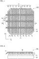
FIG. 1 is a plan view of a multi-junction photoelectric conversion device according to one embodiment. -
FIG. 2 is a sectional view taken along line A-A inFIG. 1 . -
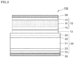
FIG. 3 is a schematic sectional view showing one example of a stacking configuration of a multi-junction photoelectric conversion unit. -
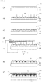
FIG. 4 is a process conceptual diagram of one example of a process for manufacturing a multi-junction photoelectric conversion device. -
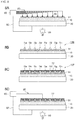
FIG. 5 is a process conceptual diagram of one example of a process for manufacturing a multi-junction photoelectric conversion device. -
FIG. 6 is a plan view of a stacked unit in which a separation groove is filled with an insulating material. -
FIG. 7 is a process conceptual diagram of one example of a process for manufacturing a multi-junction photoelectric conversion device. -
FIG. 8 is a process conceptual diagram of one example of a process for manufacturing a multi-junction photoelectric conversion device. -
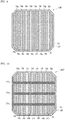
FIG. 9 is a plan view of a stacked unit in which a finger electrode is disposed so as to fill a separation groove. -
FIG. 10 is a plan view of a stacked unit in which a bus bar electrode is disposed so as to connect the finger electrode of the stacked unit ofFIG. 9 . -
FIG. 1 is a plan view of a multi-junctionphotoelectric conversion device 100 according to one embodiment of the present invention, andFIG. 2 is a sectional view taken along line A-A inFIG. 1 . The photoelectric conversion device according to the present invention is a multi-junction photoelectric conversion device in which a firstphotoelectric conversion unit 10 and a secondphotoelectric conversion unit 20 are stacked and connected in series. - The multi-junction
photoelectric conversion device 100 has afirst electrode 51 on the firstphotoelectric conversion unit 10. Thefirst electrode 51 is patterned in stripe, separated by aseparation groove 59 extending in a second direction (y direction), and divided into belt-like small-area regions 51a to 51i arranged in a first direction (x direction).Finger electrodes 71a to 71i extending in the second direction are disposed on the belt-like regions 51a to 51i, respectively. Thefinger electrodes 71a to 71i are electrically connected through an electroconductive wiring member (interconnector) 81 disposed on the finger electrodes. Theinterconnector 81 provided in the multi-junctionphotoelectric conversion device 100 is electrically connected to an adjacent photoelectric conversion device to modularize the photoelectric conversion devices. -
FIG. 3 is a schematic sectional view showing one embodiment of a multi-junction unit in which the firstphotoelectric conversion unit 10 and the secondphotoelectric conversion unit 20 are stacked. Afirst electrode 50 is disposed on a surface on the firstphotoelectric conversion unit 10 side, and asecond electrode 55 is disposed on a surface on the secondphotoelectric conversion unit 20 side. - The first
photoelectric conversion unit 10 includes a first semiconductor layer which is a thin film as aphotoelectric conversion layer 11. The first semiconductor layer absorbs light to generate photocarriers. Examples of the thin-film that forms thefirst semiconductor layer 11 include silicon-based semiconductor thin-films of amorphous silicon, microcrystalline silicon, and the like; compound semiconductor thin-films of CIS, CIGS, and the like; organic semiconductor thin-films; and organic-inorganic hybrid semiconductor thin-films. - As the organic-inorganic hybrid semiconductor, a perovskite thin-film containing a photosensitive material having a perovskite-type crystal structure may be used. The compound that forms the perovskite-type crystal material is represented by, for example, a general formula of R1NH3M1X3 or HC(NH2)2M1X3. In the formula, R1 is an alkyl group, preferably an alkyl group having 1 to 5 carbon atoms, especially preferably a methyl group. M1 is a divalent metal ion, preferably Pb or Sn. X is a halogen, and examples thereof include F, CI, Br and I. All three Xs may be the same halogen element, or include a plurality of halogens.
- A compound represented by a formula CH3(NH3)Pb(I1-xBrx)3, where 0 ≤ x ≤ 1, is a preferable example of a compound that constitute the perovskite-type crystal material. The spectral sensitivity characteristic can be adjusted by changing the type and ratio of the halogen. A perovskite semiconductor thin-film may be formed by any kinds of dry processes or solution casting methods such as spin coating.
- The
photoelectric conversion unit 10, which includes a perovskite semiconductor thin-film as thephotoelectric conversion layer 11, has charge transport layers 14 and 15. One of the charge transport layers 14 and 15 is a hole transport layer, and the other is an electron transport layer. - Examples of the material of the hole transport layer include polythiophene derivatives such as poly-3-hexylthiophene (P3HT) and poly(3,4-ethylenedioxythiophene) (PEDOT), fluorene derivatives such as 2,2',7,7'-tetrakis-(N,N-di-p-methoxyphenylamine)-9,9'-spirobifluorene (Spiro-OMeTAD), carbazole derivatives such as polyvinyl carbazole, triphenylamine derivatives, diphenylamine derivatives, polysilane derivatives and polyaniline derivatives. Examples of the material of the electron transport layer include metal oxides such as titanium oxide, zinc oxide, niobium oxide, zirconium oxide and aluminum oxide.
- When the first
photoelectric conversion unit 10 is a silicon-based thin-film photoelectric conversion unit including a pin junction, thefirst semiconductor layer 11 is an intrinsic (i-type) silicon-based thin-film. Examples of the silicon-based thin-film include thin-films of amorphous silicon, an amorphous silicon alloy, microcrystalline silicon, a microcrystalline silicon alloy, and the like. Examples of the silicon alloy include silicon carbide, silicon oxide, silicon nitride, and silicon germanium. When the firstphotoelectric conversion unit 10 includes a pin junction, one of conductive semiconductor layers 14 and 15 is a p-type semiconductor layer, and the other is an n-type semiconductor layer. - The
first semiconductor layer 11 is not limited to a perovskite-type crystal material or a silicon-based material, and various semiconductor thin-films usable as a photoelectric conversion layer can be used. A charge transport layer and conductive semiconductor layers 14 and 15 adjacent to thefirst semiconductor layer 11 can be appropriately selected according to the material of the photoelectric conversion layer, and the like. - The second
photoelectric conversion unit 20 includes a second semiconductor layer as aphotoelectric conversion layer 21. The second semiconductor layer absorbs light to generate photocarriers. Thesecond semiconductor layer 21 has a band gap different from that of thefirst semiconductor layer 11. Thus, thefirst semiconductor layer 11 and thesecond semiconductor layer 21 have spectral sensitivity characteristics in different wavelength ranges. Thus, light having a wavelength in a wider range can be involved in photoelectric conversion in a stacked photoelectric conversion unit in which the firstphotoelectric conversion unit 10 including thefirst semiconductor layer 11 as a photoelectric conversion layer and the secondphotoelectric conversion unit 20 including thesecond semiconductor layer 21 as a photoelectric conversion layer are stacked. When thefirst semiconductor layer 11 has a band gap wider than that of thesecond semiconductor layer 21, the light-receiving surface is on the firstphotoelectric conversion unit 10 side. - The
second semiconductor layer 21 may be either a semiconductor thin-film or a semiconductor substrate. Examples of the semiconductor thin-film are as described above. Examples of the semiconductor substrate include silicon substrates of single-crystalline silicon, polycrystalline silicon, or the like, and crystalline semiconductor substrates of germanium, gallium nitride, or the like. - When the
second semiconductor layer 21 is a single-crystalline silicon substrate, examples of the secondphotoelectric conversion unit 20 include diffusion-type cells in which a diffusion layer of second conductivity-type is formed on the light-receiving side of a single-crystalline silicon substrate of first conductivity-type, and heterojunction cells in which a silicon-based thin-film is disposed on both surfaces of a single-crystalline silicon substrate of first conductivity-type. - The
heterojunction cell 20 including a single-crystalline silicon substrate as thesecond semiconductor layer 21, and including a silicon-based thin-film on both surfaces of the single-crystalline silicon substrate has conductive silicon-based thin-films crystalline silicon substrate 21 may be either a p-type single-crystalline silicon substrate or an n-type single-crystalline silicon substrate. Since comparison between a hole and an electron shows that the electron has a higher mobility, excellent conversion characteristics are exhibited particularly when an n-type single-crystalline silicon substrate is used. One of the conductive silicon-based thin-films - The second
photoelectric conversion unit 20 is connected to the firstphotoelectric conversion unit 10 in series. Thus, the conductivity-types of the conductive silicon-based thin-films photoelectric conversion unit 10 and the secondphotoelectric conversion unit 20 are identical to each other. For example, when the firstphotoelectric conversion unit 10 is a perovskite cell, thecharge transport layer 14 on thefirst electrode 51 side is a hole transport layer, and thecharge transport layer 15 on the secondphotoelectric conversion unit 20 side is an electron transport layer, the conductive silicon-based thin-film 24 on the firstphotoelectric conversion unit 10 side in the secondphotoelectric conversion unit 20 is a p-type conductive silicon-based thin-film, and the other conductive silicon-based thin-film 25 in the secondphotoelectric conversion unit 20 is an n-type conductive silicon-based thin-film. The same applies when the first photoelectric conversion unit has a pin or pn semiconductor junction from thefirst electrode 51 side. - It is preferable that intrinsic silicon-based thin-
films crystalline silicon substrate 21 and the conductive silicon-based thin-films films crystalline silicon substrate 21 can enhance the passivation effect on the surfaces of the single-crystalline silicon substrate 21. - An
intermediate layer 13 may be disposed between the firstphotoelectric conversion unit 10 and the secondphotoelectric conversion unit 20. Theintermediate layer 13 is provided for adjustment of a band gap between two photoelectric conversion units stacked, selective movement of carriers, formation of a tunnel junction, wavelength selective reflection, and so on. The configuration of the intermediate layer is selected according to the type, combination, and the like of thephotoelectric conversion units photoelectric conversion unit 10 and the secondphotoelectric conversion unit 20, the intermediate layer may be omitted. - Preferably, the
first electrode 50 on a surface on the firstphotoelectric conversion unit 10 side and thesecond electrode 55 on a surface on the secondphotoelectric conversion unit 20 side are disposed on substantially the entire surface of the photoelectric conversion unit for effectively extracting photoproduction carriers. The electrode disposed on a surface on the light-receiving side is preferably a transparent electrode. In other words, when the firstphotoelectric conversion unit 10 is a top cell on the light-receiving side, thefirst electrode 50 is preferably a transparent electrode. The electrode on the rear side may be either a transparent electrode or a metal electrode. As a material of the transparent electrode, a metal oxide such as ITO, zinc oxide or tin oxide is preferably used. As a material of the metal electrode, silver, copper, aluminum, or the like is preferably used. - In the manufacturing method according to the present invention, a patterned first electrode is disposed on a surface of a first photoelectric conversion unit of a stacked unit in which the first photoelectric conversion unit and a second photoelectric conversion unit are stacked, and reverse bias processing is performed in a state in which the patterned electrode is electrically separated.
- Hereinafter, with reference to
FIGS. 4A to 4F , one embodiment of a method for manufacturing a multi-junctionphotoelectric conversion device 100 shown inFIGS. 1 and 2 will be described. - First, as shown in
FIG. 4A , astacked unit 101 is prepared in which a firstphotoelectric conversion unit 10 and a secondphotoelectric conversion unit 20 are stacked and connected in series. When a photoelectric conversion layer of the secondphotoelectric conversion unit 20 is a semiconductor substrate such as a silicon substrate, it is preferable to form the firstphotoelectric conversion unit 10 stacking on the secondphotoelectric conversion unit 20. - When a semiconductor substrate such as a silicon substrate is used as the photoelectric conversion layer of the second photoelectric conversion unit, there are no pinholes and the like in the photoelectric conversion layer. On the other hand, since the photoelectric conversion layer of the first
photoelectric conversion unit 10 is a thin-film, defects such as pinholes are unavoidably generated during deposition. - As shown in
FIG. 4B , afirst electrode 51 is formed on the firstphotoelectric conversion unit 10. When defects such as pinholes exist in the first photoelectric conversion unit, an electroconductive material of the first electrode comes into contact with the defective portions, or the electroconductive material is embedded in the pinholes, resulting in formation of a leakage portion. - The
first electrode 51 is separated by aseparation groove 59, and has a plurality ofregions 51a to 51i. Examples of the method for forming a patterned electrode include a method in which patterning is performed during deposition; and a method in which after formation of an electrode layer, a separation groove is formed, and patterning is performed. Examples of the method for forming a patterned electrode include a method in which a film is deposited while a separation groove 59-formed region on the firstphotoelectric conversion unit 10 is covered with a mask. Examples of the method for forming theseparation groove 59 after formation of an electrode layer include a method in which an electrode layer in a separation groove-formed region is eliminated by wet etching or the like (pattern etching); and a method in which an electrode layer is irradiated with laser light. - A second electrode (not shown) may be disposed on a surface on the second
photoelectric conversion unit 20 side. When photoirradiation is performed from the secondphotoelectric conversion unit 20 side during reverse bias processing, preferably, the second electrode is a transparent electrode. When light can reach the second photoelectric conversion unit, a metal electrode may be provided as the second electrode. For example, a patterned metal electrode such as a finger electrode or a bus bar electrode may be disposed on the transparent electrode. In addition, the second electrode may have a stacking structure of a transparent electrode and a metal electrode with the metal electrode disposed on the transparent electrode after reverse bias processing. - As shown in
FIG. 4C , afinger electrode 71 is disposed on each region of the patternedfirst electrode 51. The finger electrode is provided for extracting carriers, which have reached thefirst electrode 51 from the photoelectric conversion layer, to the outside. In addition, in the present embodiment, thefinger electrode 71 is used as a power supply electrode during reverse bias processing. When thefirst electrode 51 is a transparent electrode, a potential difference in the surface of the electrode is reduced by providing themetallic finger electrode 71. Thus, in reverse bias processing, a uniform voltage can be applied over the entire region of each ofelectrodes 51a to 51i, and leakage can be uniformly eliminated irrespective of the distance from the power supply point. - As a material of the finger electrode, a low-resistance metallic material such as silver, copper, or aluminum is preferably used. The finger electrode is formed in a pattern shape by a method in which an electroconductive paste is applied; a plating method; or the like.
- The
finger electrode 71 is provided so as to maintain a state in which a plurality ofregions 51a to 51i of thefirst electrode 51 are electrically separated. In other words, thefinger electrode 71 is disposed so as not to overlap theseparation groove 59. Preferably, thefinger electrode 71 is disposed so as to extend in parallel with theseparation groove 59 as shown inFIG. 1 . - Leakage in the first
photoelectric conversion unit 10 is eliminated by reverse bias processing in a state in which thefirst electrode 51 disposed on the firstphotoelectric conversion unit 10 is separated into a plurality ofregions 51a to 51i.FIG. 4D is a conceptual diagram of a reverse bias processing step. - In the form shown in
FIG. 4D , each offinger electrodes 71 disposed in regions of thefirst electrode 51 is connected to apower supply 90 through awire 91, and the secondphotoelectric conversion unit 20 is connected to thepower supply 90 through awire 92. When asecond electrode 55 is formed on a surface of the secondphotoelectric conversion unit 20 as in the stacked-layer form shown inFIG. 3 , it is preferable that thewire 92 be connected to the second electrode. Thepower supply 90 is configured such that power can be supplied to any of a plurality ofwires 91a to 91i. - In reverse bias processing, a stack of the first
photoelectric conversion unit 10 and the secondphotoelectric conversion unit 20 is irradiated with light from alight source 99. Thelight source 99 is not particularly limited as long as it outputs light in such a wavelength range that the second semiconductor layer as a photoelectric conversion layer of the secondphotoelectric conversion unit 20 can absorb the light, and it is capable of uniformly irradiating the second photoelectric conversion unit with light. Examples of the light source include LEDs and halogen lamps. The light source may be a pulsed light source. A wavelength selection filter (not shown) may be arranged between thelight source 99 and the stacked unit to adjust the wavelength range of light applied to the photoelectric conversion unit. - Light from the
light source 99 is applied preferentially to the secondphotoelectric conversion unit 20 over the firstphotoelectric conversion unit 10. That is, light is applied so as to generate a larger photocurrent in the secondphotoelectric conversion unit 20 than in the firstphotoelectric conversion unit 10. For example, by applying light having a wavelength at which the light is absorbed in a small amount in the first photoelectric conversion unit, and absorbed in a large amount in the second photoelectric conversion unit, the second photoelectric conversion unit can be preferentially irradiated with light. For example, a perovskite semiconductor layer hardly absorbs light having a wavelength longer than 800 nm, and therefore by applying infrared light having a wavelength longer than 800 nm to a multi-junction unit including a perovskite cell as the firstphotoelectric conversion unit 10, and a crystalline silicon cell as the secondphotoelectric conversion unit 20, the second photoelectric conversion unit can be preferentially irradiated with light. - In addition, also when a white light source is used as the
light source 99, application of light from the second photoelectric conversion unit (crystalline silicon cell) 20 side causes most of the light to be absorbed by the crystalline silicon substrate of thecrystalline silicon cell 20, and thus prevented from reaching theperovskite cell 10, so that the crystalline silicon cell can be preferentially irradiated with light. Thus, when the first semiconductor layer of the firstphotoelectric conversion unit 10 has a band gap wider than that of the second semiconductor layer of the secondphotoelectric conversion unit 20, i.e., in the case where the firstphotoelectric conversion unit 10 and the secondphotoelectric conversion unit 20 are top cell and bottom cell, respectively, in a multi-junction unit, the second photoelectric conversion unit can be preferentially irradiated with light by applying light from the secondphotoelectric conversion unit 20 side (the rear side during power generation). - A reverse bias voltage is applied from the
power supply 90 to the stacked unit while the second photoelectric conversion unit is preferentially irradiated with light to generate photocarriers. When a p-type semiconductor (or hole transport layer) is on the first electrode side, i.e. the stacked unit is a p-front-type stacked unit, a voltage is applied in such a manner that thefirst electrode 51 on the firstphotoelectric conversion unit 10 is negative, and the secondphotoelectric conversion unit 20 side is positive. In the case of an n-front type, a voltage is applied in such a manner that thefirst electrode 51 is positive, and the secondphotoelectric conversion unit 20 side is negative. - When a reverse bias voltage is applied, a current locally passes into a leakage portion in the first photoelectric conversion unit, leading to recombination with photocarriers generated in the second photoelectric conversion unit. Thus, when a reverse bias voltage is applied while the second photoelectric conversion unit is preferentially irradiated with light, a current passes between the front and rear electrodes that sandwich the
photoelectric conversion units - In the present invention, a reverse bias voltage is applied between a specific region of the
first electrodes 51a to 51i obtained by dividing the first electrode into a plurality of regions and the second photoelectric conversion unit. As described above, thepower supply 90 is configured such that a voltage can be applied to any of a plurality ofwires 91a to 91i, and therefore a reverse bias voltage can be selectively applied between a specific region of the first electrode divided into a plurality of regions and the second photoelectric conversion unit.FIG. 4E schematically shows a case in which a reverse bias voltage is applied between thewire 91a connected to thefinger electrode 71a and thewire 92 while light is irradiated from the secondphotoelectric conversion unit 20 side, so that leakage in theregion 10a of the first photoelectric conversion unit existing under theelectrode 51a is eliminated. - Here, a voltage is applied to the
electrode 51a in thefirst electrode 51 divided into nineregions 51a to 51h in the drawing. Since a voltage is applied between the secondphotoelectric conversion unit 20 and theelectrode 51a, a reverse bias current locally passes into a leakage portion existing in theregion 10a of the first photoelectric conversion unit existing under theelectrode 51a, so that leakage in theregion 10a is eliminated. In contrast, in regions other than theregion 10a of the firstphotoelectric conversion unit 10, a reverse bias voltage is not applied, and therefore even when a leakage portion exists, a reverse bias current does not pass, and thus leakage is not eliminated. - A voltage is applied from the
power supply 90 to theelectrode 51a through thewire 91a to eliminate leakage in theregion 10a just below theelectrode 51a, and a voltage is then sequentially applied toelectrodes 51b to 51i through wires 91b to 91i to eliminate leakage in the photoelectric conversion unit existing under respective small-area regions. - When a large number of leakage portions existing over the entire surface of the photoelectric conversion unit are to be eliminated at a time, it is necessary that a reverse bias current necessary for elimination of leakage pass into each leakage portion, so that the total current amount may increase, leading to expansion of pinholes and breakage of an element. On the other hand, in the present invention, leakage in a region just below the
electrode 51a is selectively eliminated by selectively applying a reverse bias voltage to theelectrode 51a divided into small-area parts, so that the total current amount is not excessively large, and thus expansion of the pinhole and breakage of an element can be suppressed. - When a plurality of cells separated by a separation groove are connected in series in an in-plane direction to form an array, a reverse bias current passes through the whole array connected in series, and therefore it is difficult to positionally selectively eliminate leakage. For eliminating leakage in a specific region, it is necessary that a reverse bias current be caused to pass exclusively into a leakage portion with a photocurrent generated by selectively applying light to a region to be subjected to elimination of leakage in such a manner that the photoelectric conversion unit in the specific region does not behave as a resistor. Thus, it is necessary to adjust the relative position between the light source and the multi-junction photoelectric conversion unit. On the other hand, in the method of the present invention in which the photoelectric conversion unit is not separated, and reverse bias processing is performed with only electrodes separated from one another, adjustment of the relative position with the light source is not required at the time of changing a region to which a reverse bias voltage is applied. Thus, the method of the present invention is excellent in workability in sequential reverse bias processing of a plurality of separated small-area regions.
- In addition, in the method of the present invention, it is not necessary to pattern the photoelectric conversion layer, and therefore a decrease in light-receiving area of the photoelectric conversion layer is small. Thus, a multi-junction photoelectric conversion device, which generates a large amount of power and which hardly suffers deterioration of characteristics due to leakage in a thin-film, can be obtained.
- Preferably, a plurality of
regions 51a to 51i of the first electrode, which are separated from one another, are electrically connected after leakage in the first photoelectric conversion unit is eliminated by reverse bias processing. Examples of the method for electrically connecting first electrodes separated from one another include a method in which theseparation grooves 59 is filled with an electroconductive material to bring separated small-area electrodes 51a to 51i into conduction with one another; and a method in which an electroconductive material is disposed on the first electrode so as to extend over a plurality of regions. - Examples of the electroconductive material disposed on the first electrode so as to extend over a plurality of regions include various electrode materials, and wiring members such as interconnectors. Such an electroconductive material may be disposed so as to be in contact with the
first electrode 51, or disposed so as to be in conduction with theelectrode 51 through another electrode or the like. For reducing a current collection loss, the electroconductive material disposed on the first electrode is preferably a low-resistance metallic material. - In
FIG. 4F , aninterconnector 81 for electrically connecting adjacent cells is connected to thefinger electrode 71 on thefirst electrode 51, so that a plurality ofregions 51a to 51i of the first electrode, which are separated from one another by theseparation groove 59, are electrically connected. Thefinger electrode 71 and theinterconnector 81 are electrically connected using solder, an electroconductive adhesive, or the like. - When in an operation of connecting the
finger electrode 71 to theinterconnector 81, an electroconductive material such as solder or an electroconductive adhesive flows out into the separation groove that separates thefirst electrode 51, the electroconductive material may come into contact with the photoelectric conversion unit, resulting in a failure such as leakage. Particularly, when theseparation groove 59 extends to the inside of the firstphotoelectric conversion unit 10, ingress of the electroconductive material into the separation groove may cause critical leakage, and therefore it is necessary to pay attention to prevent ingress of the electroconductive material into the separation groove. - As in an embodiment shown in
FIG. 5 , contact between aphotoelectric conversion unit 10 and an electroconductive material may be prevented by filling aseparation groove 59 with an insulating material before connection of an electroconductive member.FIGS. 5A to 5F are process conceptual diagrams of one embodiment of the manufacturing method according to the present invention. In this embodiment, aninterconnector 81 is mounted after theseparation groove 59 is filled with the insulating material. First, astacked unit 111 of the firstphotoelectric conversion unit 10 and a secondphotoelectric conversion unit 20 is prepared. The stacked unit is the same as thestacked unit 101 inFIG. 4A . - Next, a first electrode layer is formed on the first
photoelectric conversion unit 10, and theseparation groove 59 is formed by applying laser light LB, so that a first electrode is patterned in a plurality of small-area regions. For electrically separating the electrode layer, it is necessary to form the separation groove so as to extend to the interface between anelectrode 51 and thephotoelectric conversion unit 10. It is difficult to stop formation of the separation groove at the interface portion, and therefore for reliably separating the electrode, theseparation groove 59 is formed so as to extend to thephotoelectric conversion unit 10 as shown inFIG. 5B . Preferably, theseparation groove 59 does not extend to the secondphotoelectric conversion unit 20. - After formation of the separation groove, the
finger electrode 71 is formed on the first electrode 51 (FIG. 5C ). Thereafter, as in the case of the above-described embodiment, leakage in the firstphotoelectric conversion unit 10 is eliminated by applying a reverse bias voltage while preferentially irradiating the secondphotoelectric conversion unit 20 with light from a light source 99 (FIG. 5D ). - Thereafter, a plurality of regions of the first electrode are electrically connected by disposing an electroconductive material so as to extend over a plurality of regions of the first electrode. Examples of the electroconductive material disposed so as to extend over a plurality of regions of the first electrode include wiring members (interconnectors) for interconnection, and bus bar electrodes.
FIG. 5F shows an example in which a plurality offinger electrodes 71 are connected by theinterconnector 81. - In this embodiment, an insulating
layer 61 is formed, and theseparation groove 59 is filled with an insulating material as shown inFIG. 5E before the interconnector or bus bar electrode is provided so as to extend over a plurality of regions of the first electrode. By filling theseparation groove 59 with the insulating material, an exposed portion of the photoelectric conversion unit is protected with the insulating material even when the separation groove formed by laser processing or the like extends to thephotoelectric conversion unit 10. Thus, a metallic material constituting the bus bar electrode, or the electroconductive material used for connecting the interconnector does not enter the separation groove to come into contact with thephotoelectric conversion unit 10, and thus occurrence of leakage due to the electroconductive material is suppressed. - The insulating
layer 61 may be disposed in such a manner that the insulating material fills the separation groove in the region where theinterconnector 81 is to be arranged thereover.FIG. 6 is a plan view of astacked unit 115 inFIG. 5E , where the insulatinglayer 61 is formed in a belt-shape extending in a direction perpendicular to theseparation groove 59. Thefinger electrode 71 is not embedded in the insulatinglayer 61, and thus is exposed. - As shown in
FIG. 5F , theinterconnector 81 is disposed on thefinger electrode 71 to electrically connect a plurality of finger electrodes. Preferably, theinterconnector 81 is arranged in an insulating layer-formed region with a width smaller than that of the insulatinglayer 61. By forming the insulatinglayer 61 with a width larger than that of theinterconnector 81, ingress of the electroconductive material into the separation groove during interconnection can be more reliably prevented. - Although
FIG. 6 shows an embodiment in which the insulatinglayer 61 is formed in a belt-shape, the shape of the insulating layer is not particularly limited as long as the separation groove is filled with an insulating material in a region where a bus bar electrode or interconnector for electrically connecting the patterned first electrode is arranged. For example, when the separation groove is filled with an insulating material, the insulating material is not required to be disposed on thefirst electrode 51. In addition, when the insulating material is light-transmissive, an insulating layer may be disposed on the entire surface except a finger electrode 71-formed region. - Although
FIG. 5 shows an embodiment in which theseparation groove 59 is filled with an insulating material after reverse bias processing, the separation groove may be filled with the insulating material before reverse bias processing. - In each of the above-described embodiments, the
finger electrodes 71 disposed on each of a plurality of regions of thefirst electrode 51, which are separated from one another, are connected through an interconnector or bus bar electrode, so that a plurality of regions of the first electrode are electrically connected. As another embodiment, a separation groove separating afirst electrode 51 may be filled with an electroconductive material such as a metal or a conductive oxide to electrically connect a plurality of regions of the first electrode. -
FIGS. 7A to 7E are process conceptual diagrams of an embodiment in which a plurality of regions of the first electrode are electrically connected by filling aseparation groove 59 with a conductive oxide. - First, as in
FIG. 4A , astacked unit 121 of a firstphotoelectric conversion unit 10 and a secondphotoelectric conversion unit 20 is prepared (FIG. 7A ), and as inFIG. 4B , afirst electrode 51 patterned by theseparation groove 59 is formed (FIG. 7B ). In this embodiment, the separation groove is filled with an electroconductive material after elimination of leakage by reverse bias processing, and therefore it is preferable that theseparation groove 59 do not extend to the inside of the firstphotoelectric conversion unit 10. It is therefore preferable that theseparation groove 59 be formed by mask deposition or pattern etching. - Leakage is eliminated by reverse bias processing with the patterned
first electrode 51 disposed on the photoelectric conversion unit 10 (FIG. 7C ). In this embodiment, a metal electrode is not formed on thefirst electrode 51, and therefore awire 93 from apower supply 90 is connected onto thefirst electrode 51. Leakage in the firstphotoelectric conversion unit 10 is eliminated by applying a reverse bias voltage while preferentially irradiating the secondphotoelectric conversion unit 20 with light from alight source 99. - For facilitating electrical connection between the
first electrode 51 and the wiring, thewire 93 may be equipped with aprobe electrode 96 at the tip. The shape of the probe electrode is not particularly limited. When the probe electrode has a plate shape, the applied voltage can be made uniform because the contact area between the first electrode and the probe electrode is large, and the potential in the surface is uniform. - After elimination of leakage by reverse bias processing, the
separation groove 59 is filled with an electroconductive material, so that a plurality of regions of the first electrode are electrically connected. InFIG. 7D , atransparent electroconductive layer 52 is deposited on the patternedfirst electrode 51 to fill theseparation groove 59 with a transparent electroconductive material that forms the transparent electroconductive layer. Preferably, thetransparent electroconductive layer 52 is not patterned, and is formed on the entire surface of each of thefirst electrode 51 and theseparation groove 59. - After the
separation groove 59 is filled with the electroconductive material, elimination of leakage by application of a reverse bias voltage (second reverse bias processing) may be further performed. As shown inFIG. 7C , a reverse bias voltage is sequentially applied to each region of the patternedelectrode 51 to eliminate leakage in the firstphotoelectric conversion unit 10, so that leakage in thephotoelectric conversion unit 10 under a first electrode 51-formed region is eliminated (first reverse bias processing). On the other hand, since reverse bias processing is not performed under a separation groove 59-formed region, a leakage portion may remain. After the separation groove is filled with the electroconductive material, second reverse bias processing is performed by applying a reverse bias voltage between the second photoelectric conversion unit electrically connected to thepower supply 90 through thewire 92 and thefirst electrode 51 electrically connected to thepower supply 90 through thewire 94, so that leakage remaining in the first photoelectric conversion unit under the separation groove 59-formed region can be eliminated. In the second reverse bias processing after theseparation groove 59 is filled with the electroconductive material, a reverse bias voltage is applied while the secondphotoelectric conversion unit 20 is preferentially irradiated with light from alight source 99, as in the first reverse bias processing. - Since a plurality of regions of the
first electrode 51 are electrically connected, a reverse bias voltage is applied to the entire region on the firstphotoelectric conversion unit 10 in the second reverse bias processing. For reducing a potential difference in the surface, a reverse bias voltage may be applied through ametal plate 97 connected to thewire 94 as shown inFIG. 7E . In addition, a potential difference in the surface may be reduced by applying a reverse bias voltage after a metal electrode such as a finger electrode or a bus bar electrode is disposed on thetransparent electroconductive layer 52. - Leakage in the first
photoelectric conversion unit 10 under the first electrode 51-formed region is eliminated by the foregoing first reverse bias processing, and therefore in the second reverse bias processing after theseparation groove 59 is filled with the electroconductive material, a current passes only through a leakage portion remaining in the separation groove-formed region even though a reverse bias is applied to the entire surface. Thus, it is possible to eliminate leakage under the separation groove-formed region without passage of an excessively large current. - The area of a region to be subjected to elimination of leakage in the second reverse bias processing is preferably comparable to the area of one region of the
first electrode 51 separated by the separation groove. This can prevent a situation in which the total amount of currents for elimination of leakage is excessively large when a reverse bias voltage is applied to the entire surface. The area of the region to be subjected to elimination of leakage is substantially equal to the total of the areas of the separation grooves filled with the electroconductive material. When thefirst electrode 51 is patterned in stripe, it is preferable that the width W of one region of the first electrode be substantially equal to the total of the widths x1 to x8 of the separation grooves. Specifically, the total of the widths of the separation grooves is preferably not more than twice the width W of one region of the first electrode. - When the area of the region to be subjected to elimination of leakage in the second reverse bias processing is comparable to the area of one region of the
first electrode 51, passage of an excessively large current is not required for elimination of leakage because the total current amount in the second reverse bias processing is comparable to the current amount in application of a reverse bias voltage to each electrode region in the first reverse bias processing. - After the second bias processing, formation of a metal electrode such as a finger electrode or a bus bar electrode and connection of the interconnector on the metal electrode may be performed.
-
FIGS. 8A to 8D are process conceptual diagrams of an embodiment in which a plurality of regions of the first electrode are electrically connected by filling aseparation groove 59 with a metallic material. First, as inFIGS. 7A to 7C , a stacked unit of a firstphotoelectric conversion unit 10 and a secondphotoelectric conversion unit 20 is prepared, afirst electrode 51 patterned by theseparation groove 59 is formed, and first reverse bias processing is performed (FIG. 8A ). - After the first reverse bias processing, the
separation groove 59 is filled with a metallic material. InFIG. 8B , afinger electrode 73 is formed so as to fill theseparation groove 59.FIG. 9 is a plan view of astacked unit 136 inFIG. 8B in whichfinger electrodes 73a to 73h are formed so as to fill the separation groove. Preferably, thefinger electrode 73 is formed over substantially the entire length of theseparation groove 59. In addition, it is preferable that thefinger electrode 73 be formed to have a width larger than that of theseparation groove 59. When thefinger electrode 73 is formed to have a width larger than that of the separation groove, theseparation groove 59 is filled with a metallic material to electrically connect regions of the patterned first electrode, and the contact area between the finger electrode and the first electrode can be increased to improve carrier collection efficiency. - After formation of the finger electrode, a
bus bar electrode 77 extending in a direction perpendicular to thefinger electrode 73 is formed (FIG. 8C ).FIG. 10 is a plan view of astacked unit 137 after formation of thebus bar electrode 77. By formingbus bar electrodes 77a to 77c onfinger electrodes 73a to 73h, a plurality of finger electrodes are electrically connected. As a material of the bus bar electrode, a low-resistance metallic material such as silver, copper or aluminum is preferably used. The bus bar electrode is formed by a printing method, a plating method, or the like. AlthoughFIGS. 8B and 8C show an example in which thebus bar electrode 77 is formed after the formation of thefinger electrode 73, the bus bar electrode and the finger electrode may be formed simultaneously. - After formation of the bus bar electrode, remaining leakage in the
photoelectric conversion unit 10 under a separation groove 59-formed region may be eliminated by performing second reverse bias processing while preferentially irradiating the secondphotoelectric conversion unit 20 with light from alight source 99 as in the case of the embodiment 3. InFIG. 8D , awire 95 from apower supply 90 is connected to thebus bar electrode 77. In this embodiment, power is supplied from thebus bar electrode 77 to thefinger electrode 71 to apply a reverse bias voltage between thefinger electrode 71 and the second photoelectric conversion unit, so that leakage remaining in the first photoelectric conversion unit under a finger electrode 71-formed region (separation groove 59-formed region) is eliminated. - The second bias processing may be performed before the formation of the bus bar electrode. In this case, the wire from the
power supply 90 may be connected to thefinger electrode 71 to supply power, or a metal plate or the like connected to the wire may be brought into contact with a plurality of finger electrodes to supply power to the finger electrodes. - An interconnector may be mounted on the
bus bar electrode 77. The interconnector electrically connected to the bus bar electrode is electrically connected to an adjacent photoelectric conversion device to modularize the photoelectric conversion devices. - Each of the embodiments 1 to 4 is illustrative, and constituent elements such as electrodes and electroconductive materials which form the multi-junction photoelectric conversion devices, steps, and so on in the embodiments can be appropriately combined to carry out the manufacturing method according to the present invention.
- In practical use of the photoelectric conversion devices, it is preferable that the multi-junction photoelectric conversion device in which leakage in the thin-film photoelectric conversion layer of the first photoelectric conversion unit is eliminated by the method according to the present invention be encapsulated by an encapsulant to be modularized. Modularization of photoelectric conversion devices may be performed by an appropriate method. For example, adjacent cells are electrically connected in series or in parallel through an interconnector, and then encapsulated with an encapsulant and a glass plate.
-
- 10
- first photoelectric conversion unit
- 11
- first semiconductor layer (photoelectric conversion layer)
- 20
- second photoelectric conversion unit
- 21
- second semiconductor layer (photoelectric conversion layer)
- 50, 51
- first electrode
- 59
- separation groove
- 55
- second electrode
- 61
- insulating layer
- 71, 73
- finger electrode
- 77
- bus bar electrode
- 81
- wiring member (interconnector)
- 90
- power supply
- 99
- light source
- 100
- multi-junction photoelectric conversion device
- 101 to 104
- stacked unit
Claims (15)
- A method for manufacturing a multi-junction photoelectric conversion device comprising: a first electrode; a first photoelectric conversion unit including a first semiconductor layer as a photoelectric conversion layer, the first semiconductor layer being a thin film; and a second photoelectric conversion unit including a second semiconductor layer as a photoelectric conversion layer, arranged in this order, wherein the second photoelectric conversion unit is connected to the first photoelectric conversion unit in series,
the method comprising the steps of:forming a first electrode on the first photoelectric conversion unit, the first electrode being patterned in a plurality of regions separated by a separation groove; andeliminating a leakage existing in the first semiconductor layer by applying a reverse bias voltage between one region of the first electrode and the second photoelectric conversion unit,whereinthe application of the reverse bias voltage is performed in a state that the second photoelectric conversion unit is preferentially irradiated with light to generate a larger photocurrent in the second photoelectric conversion unit than in the first photoelectric conversion unit. - The method for manufacturing a multi-junction photoelectric conversion device according to claim 1, wherein the first semiconductor layer has a band gap wider than that of the second semiconductor layer, and the light-receiving surface is on the first electrode side.
- The method for manufacturing a multi-junction photoelectric conversion device according to claim 1 or 2, wherein the first electrode is a transparent electrode.
- The method for manufacturing a multi-junction photoelectric conversion device according to any one of claims 1 to 3, wherein the second semiconductor layer is a crystalline semiconductor substrate.
- The method for manufacturing a multi-junction photoelectric conversion device according to any one of claims 1 to 4, wherein the first semiconductor layer contains a photosensitive material having a perovskite-type crystal structure.
- The method for manufacturing a multi-junction photoelectric conversion device according to any one of claims 1 to 5, wherein the first electrode patterned in a plurality of regions is formed by depositing an electrode layer on the first photoelectric conversion unit, followed by irradiating the electrode layer with laser light to form the separation groove.
- The method for manufacturing a multi-junction photoelectric conversion device according to any one of claims 1 to 5, wherein the first electrode patterned in a plurality of regions is formed by depositing an electrode layer on the first photoelectric conversion unit, followed by pattern etching of the electrode layer to form the separation groove.
- The method for manufacturing a multi-junction photoelectric conversion device according to any one of claims 1 to 5, wherein the first electrode patterned in a plurality of regions is formed by depositing an electrode layer with the first photoelectric conversion unit covered with a mask, so that the separation groove is formed in a region covered with the mask.
- The method for manufacturing a multi-junction photoelectric conversion device according to any one of claims 1 to 8, wherein a metal electrode is disposed in each of a plurality of regions of the first electrode, and the metal electrode is electrically connected to a power supply to apply the reverse bias voltage.
- The method for manufacturing a multi-junction photoelectric conversion device according to any one of claims 1 to 9, wherein the method further comprising step of electrically connecting a plurality of regions of the first electrode, which are separated from one another, after carrying out the step of eliminating the leakage.
- The method for manufacturing a multi-junction photoelectric conversion device according to claim 10, wherein the separation groove is filled with an electroconductive material to electrically connect a plurality of regions of the first electrode.
- The method for manufacturing a multi-junction photoelectric conversion device according to claim 11, wherein
after the separation groove is filled with the electroconductive material, leakage in the first semiconductor layer, which remains in a separation groove-formed region, is eliminated, by applying a reverse bias voltage between the electroconductive material filled into the separation groove and the second photoelectric conversion unit in a state that the second photoelectric conversion unit is preferentially irradiated with light to generate a larger photocurrent in the second photoelectric conversion unit than in the first photoelectric conversion unit. - The method for manufacturing a multi-junction photoelectric conversion device according to claim 11 or 12, wherein after the separation groove is filled with the electroconductive material, the electroconductive material is disposed on the first electrode so as to extend over a plurality of regions of the first electrode.
- The method for manufacturing a multi-junction photoelectric conversion device according to claim 10, wherein a plurality of regions of the first electrode are electrically connected by disposing the electroconductive material on the first electrode to extend over a plurality of regions of the first electrode.
- The method for manufacturing a multi-junction photoelectric conversion device according to claim 14, wherein the separation groove is filled with an insulating material before the electroconductive material is disposed.
Applications Claiming Priority (2)
| Application Number | Priority Date | Filing Date | Title |
|---|---|---|---|
| JP2016077248 | 2016-04-07 | ||
| PCT/JP2017/005990 WO2017175491A1 (en) | 2016-04-07 | 2017-02-17 | Method for manufacturing multijunction photoelectric conversion device |
Publications (3)
| Publication Number | Publication Date |
|---|---|
| EP3442037A1 true EP3442037A1 (en) | 2019-02-13 |
| EP3442037A4 EP3442037A4 (en) | 2019-12-18 |
| EP3442037B1 EP3442037B1 (en) | 2021-02-24 |
Family
ID=60001038
Family Applications (1)
| Application Number | Title | Priority Date | Filing Date |
|---|---|---|---|
| EP17778870.0A Active EP3442037B1 (en) | 2016-04-07 | 2017-02-17 | Method for manufacturing multijunction photoelectric conversion device |
Country Status (4)
| Country | Link |
|---|---|
| US (1) | US10529882B2 (en) |
| EP (1) | EP3442037B1 (en) |
| JP (1) | JP6554230B2 (en) |
| WO (1) | WO2017175491A1 (en) |
Cited By (1)
| Publication number | Priority date | Publication date | Assignee | Title |
|---|---|---|---|---|
| WO2024175154A1 (en) * | 2023-02-20 | 2024-08-29 | Hanwha Q Cells Gmbh | Method for improving the contact resistance of a multi-solar cell |
Families Citing this family (7)
| Publication number | Priority date | Publication date | Assignee | Title |
|---|---|---|---|---|
| DE102018001057B4 (en) * | 2018-02-07 | 2025-12-04 | Ce Cell Engineering Gmbh | Method for improving the ohmic contact behavior between a contact grid and an emitter layer of a silicon solar cell |
| EP4377978A1 (en) | 2021-07-29 | 2024-06-05 | Ricoh Company, Ltd. | Photoelectric conversion element and solar cell module |
| EP4203042B1 (en) | 2021-12-22 | 2024-10-16 | Imec VZW | A method for producing a multipixel detector |
| DE102023104173B4 (en) * | 2023-02-20 | 2024-08-29 | Ce Cell Engineering Gmbh | Apparatus and method for improving the ohmic contact between a front contact grid and a doped layer of a wafer solar cell |
| DE102023104164B4 (en) * | 2023-02-20 | 2024-08-29 | Ce Cell Engineering Gmbh | Method for improving the ohmic contact between a front contact grid and a doped layer of a wafer solar cell |
| DE102023104166B4 (en) * | 2023-02-20 | 2024-08-29 | Ce Cell Engineering Gmbh | Device and method for improving the ohmic contact between a front side contact and a doped layer of a wafer solar cell |
| WO2025204282A1 (en) * | 2024-03-28 | 2025-10-02 | 株式会社カネカ | Tandem solar cell and method for manufacturing tandem solar cell |
Family Cites Families (10)
| Publication number | Priority date | Publication date | Assignee | Title |
|---|---|---|---|---|
| JPH0644638B2 (en) | 1982-12-29 | 1994-06-08 | 圭弘 濱川 | Stacked photovoltaic device with different unit cells |
| US4496788A (en) | 1982-12-29 | 1985-01-29 | Osaka Transformer Co., Ltd. | Photovoltaic device |
| JP4272320B2 (en) | 1999-12-06 | 2009-06-03 | 株式会社カネカ | Defect repair method for thin film photoelectric conversion module and method for manufacturing thin film photoelectric conversion module |
| JP4201241B2 (en) * | 2001-05-17 | 2008-12-24 | 株式会社カネカ | Method for manufacturing integrated thin film photoelectric conversion module |
| JP2003258281A (en) * | 2002-03-05 | 2003-09-12 | Fuji Electric Co Ltd | Manufacturing method of thin film solar cell |
| JP2006013403A (en) * | 2004-06-29 | 2006-01-12 | Sanyo Electric Co Ltd | SOLAR CELL, SOLAR CELL MODULE, ITS MANUFACTURING METHOD, AND ITS REPAIR METHOD |
| JP2011135058A (en) * | 2009-11-30 | 2011-07-07 | Honda Motor Co Ltd | Solar cell element, color sensor, and method of manufacturing light emitting element and light receiving element |
| US8704083B2 (en) * | 2010-02-11 | 2014-04-22 | Semiconductor Energy Laboratory Co., Ltd. | Photoelectric conversion device and fabrication method thereof |
| PL4102586T3 (en) * | 2012-09-18 | 2024-11-12 | Oxford University Innovation Limited | Optoelectronic device |
| WO2014165830A2 (en) * | 2013-04-04 | 2014-10-09 | The Regents Of The University Of California | Electrochemical solar cells |
-
2017
- 2017-02-17 WO PCT/JP2017/005990 patent/WO2017175491A1/en not_active Ceased
- 2017-02-17 JP JP2018510254A patent/JP6554230B2/en active Active
- 2017-02-17 EP EP17778870.0A patent/EP3442037B1/en active Active
-
2018
- 2018-10-05 US US16/152,608 patent/US10529882B2/en active Active
Cited By (1)
| Publication number | Priority date | Publication date | Assignee | Title |
|---|---|---|---|---|
| WO2024175154A1 (en) * | 2023-02-20 | 2024-08-29 | Hanwha Q Cells Gmbh | Method for improving the contact resistance of a multi-solar cell |
Also Published As
| Publication number | Publication date |
|---|---|
| EP3442037A4 (en) | 2019-12-18 |
| JP6554230B2 (en) | 2019-07-31 |
| US20190044016A1 (en) | 2019-02-07 |
| WO2017175491A1 (en) | 2017-10-12 |
| US10529882B2 (en) | 2020-01-07 |
| JPWO2017175491A1 (en) | 2018-11-29 |
| EP3442037B1 (en) | 2021-02-24 |
Similar Documents
| Publication | Publication Date | Title |
|---|---|---|
| US10529882B2 (en) | Method for manufacturing multijunction photoelectric conversion device | |
| KR102608733B1 (en) | Integration of bypass diodes within thin film photovoltaic module interconnects | |
| US11588124B2 (en) | Photovoltaic module | |
| US20130220396A1 (en) | Photovoltaic Device and Module with Improved Passivation and a Method of Manufacturing | |
| JP2009531871A (en) | Technology for manufacturing photovoltaic modules | |
| US20080264478A1 (en) | Thin-film solar cell and method of manufacturing the same | |
| NL2015987A (en) | Tandem solar cell and method for manufacturing such a solar cell. | |
| JP5901773B2 (en) | THIN FILM SOLAR MODULE INCLUDING SERIAL CONNECTION AND METHOD FOR SERIALLY CONNECTING A plurality of thin film solar cells | |
| US11996491B2 (en) | Solar cell module | |
| US12154727B2 (en) | Integrated bypass diode schemes for solar modules | |
| KR20220130250A (en) | Thin-film solar module with improved shunt resistance | |
| US12218263B2 (en) | Method of manufacturing a photovoltaic device | |
| KR20110080663A (en) | Solar power unit | |
| US12598856B2 (en) | Mechanically strong connections for perovskite-silicon tandem solar cells | |
| KR102891304B1 (en) | Bypass diode interconnects for thin-film solar modules | |
| US20120048358A1 (en) | Solar cell and method for manufacturing the same | |
| KR20140110177A (en) | Bifacial solar cell | |
| KR101130965B1 (en) | Solar Cell and method of manufacturing the same |
Legal Events
| Date | Code | Title | Description |
|---|---|---|---|
| STAA | Information on the status of an ep patent application or granted ep patent |
Free format text: STATUS: THE INTERNATIONAL PUBLICATION HAS BEEN MADE |
|
| PUAI | Public reference made under article 153(3) epc to a published international application that has entered the european phase |
Free format text: ORIGINAL CODE: 0009012 |
|
| STAA | Information on the status of an ep patent application or granted ep patent |
Free format text: STATUS: REQUEST FOR EXAMINATION WAS MADE |
|
| 17P | Request for examination filed |
Effective date: 20181025 |
|
| AK | Designated contracting states |
Kind code of ref document: A1 Designated state(s): AL AT BE BG CH CY CZ DE DK EE ES FI FR GB GR HR HU IE IS IT LI LT LU LV MC MK MT NL NO PL PT RO RS SE SI SK SM TR |
|
| AX | Request for extension of the european patent |
Extension state: BA ME |
|
| DAV | Request for validation of the european patent (deleted) | ||
| DAX | Request for extension of the european patent (deleted) | ||
| A4 | Supplementary search report drawn up and despatched |
Effective date: 20191118 |
|
| RIC1 | Information provided on ipc code assigned before grant |
Ipc: H01L 31/0224 20060101ALI20191112BHEP Ipc: H01L 31/078 20120101AFI20191112BHEP |
|
| GRAP | Despatch of communication of intention to grant a patent |
Free format text: ORIGINAL CODE: EPIDOSNIGR1 |
|
| STAA | Information on the status of an ep patent application or granted ep patent |
Free format text: STATUS: GRANT OF PATENT IS INTENDED |
|
| INTG | Intention to grant announced |
Effective date: 20201002 |
|
| GRAS | Grant fee paid |
Free format text: ORIGINAL CODE: EPIDOSNIGR3 |
|
| GRAA | (expected) grant |
Free format text: ORIGINAL CODE: 0009210 |
|
| STAA | Information on the status of an ep patent application or granted ep patent |
Free format text: STATUS: THE PATENT HAS BEEN GRANTED |
|
| AK | Designated contracting states |
Kind code of ref document: B1 Designated state(s): AL AT BE BG CH CY CZ DE DK EE ES FI FR GB GR HR HU IE IS IT LI LT LU LV MC MK MT NL NO PL PT RO RS SE SI SK SM TR |
|
| REG | Reference to a national code |
Ref country code: CH Ref legal event code: EP |
|
| REG | Reference to a national code |
Ref country code: AT Ref legal event code: REF Ref document number: 1365581 Country of ref document: AT Kind code of ref document: T Effective date: 20210315 |
|
| REG | Reference to a national code |
Ref country code: IE Ref legal event code: FG4D |
|
| REG | Reference to a national code |
Ref country code: DE Ref legal event code: R096 Ref document number: 602017033356 Country of ref document: DE |
|
| REG | Reference to a national code |
Ref country code: LT Ref legal event code: MG9D |
|
| REG | Reference to a national code |
Ref country code: NL Ref legal event code: MP Effective date: 20210224 |
|
| PG25 | Lapsed in a contracting state [announced via postgrant information from national office to epo] |
Ref country code: LT Free format text: LAPSE BECAUSE OF FAILURE TO SUBMIT A TRANSLATION OF THE DESCRIPTION OR TO PAY THE FEE WITHIN THE PRESCRIBED TIME-LIMIT Effective date: 20210224 Ref country code: BG Free format text: LAPSE BECAUSE OF FAILURE TO SUBMIT A TRANSLATION OF THE DESCRIPTION OR TO PAY THE FEE WITHIN THE PRESCRIBED TIME-LIMIT Effective date: 20210524 Ref country code: FI Free format text: LAPSE BECAUSE OF FAILURE TO SUBMIT A TRANSLATION OF THE DESCRIPTION OR TO PAY THE FEE WITHIN THE PRESCRIBED TIME-LIMIT Effective date: 20210224 Ref country code: GR Free format text: LAPSE BECAUSE OF FAILURE TO SUBMIT A TRANSLATION OF THE DESCRIPTION OR TO PAY THE FEE WITHIN THE PRESCRIBED TIME-LIMIT Effective date: 20210525 Ref country code: HR Free format text: LAPSE BECAUSE OF FAILURE TO SUBMIT A TRANSLATION OF THE DESCRIPTION OR TO PAY THE FEE WITHIN THE PRESCRIBED TIME-LIMIT Effective date: 20210224 Ref country code: PT Free format text: LAPSE BECAUSE OF FAILURE TO SUBMIT A TRANSLATION OF THE DESCRIPTION OR TO PAY THE FEE WITHIN THE PRESCRIBED TIME-LIMIT Effective date: 20210624 Ref country code: NO Free format text: LAPSE BECAUSE OF FAILURE TO SUBMIT A TRANSLATION OF THE DESCRIPTION OR TO PAY THE FEE WITHIN THE PRESCRIBED TIME-LIMIT Effective date: 20210524 |
|
| REG | Reference to a national code |
Ref country code: AT Ref legal event code: MK05 Ref document number: 1365581 Country of ref document: AT Kind code of ref document: T Effective date: 20210224 |
|
| PG25 | Lapsed in a contracting state [announced via postgrant information from national office to epo] |
Ref country code: RS Free format text: LAPSE BECAUSE OF FAILURE TO SUBMIT A TRANSLATION OF THE DESCRIPTION OR TO PAY THE FEE WITHIN THE PRESCRIBED TIME-LIMIT Effective date: 20210224 Ref country code: LV Free format text: LAPSE BECAUSE OF FAILURE TO SUBMIT A TRANSLATION OF THE DESCRIPTION OR TO PAY THE FEE WITHIN THE PRESCRIBED TIME-LIMIT Effective date: 20210224 Ref country code: PL Free format text: LAPSE BECAUSE OF FAILURE TO SUBMIT A TRANSLATION OF THE DESCRIPTION OR TO PAY THE FEE WITHIN THE PRESCRIBED TIME-LIMIT Effective date: 20210224 Ref country code: NL Free format text: LAPSE BECAUSE OF FAILURE TO SUBMIT A TRANSLATION OF THE DESCRIPTION OR TO PAY THE FEE WITHIN THE PRESCRIBED TIME-LIMIT Effective date: 20210224 Ref country code: SE Free format text: LAPSE BECAUSE OF FAILURE TO SUBMIT A TRANSLATION OF THE DESCRIPTION OR TO PAY THE FEE WITHIN THE PRESCRIBED TIME-LIMIT Effective date: 20210224 |
|
| PG25 | Lapsed in a contracting state [announced via postgrant information from national office to epo] |
Ref country code: IS Free format text: LAPSE BECAUSE OF FAILURE TO SUBMIT A TRANSLATION OF THE DESCRIPTION OR TO PAY THE FEE WITHIN THE PRESCRIBED TIME-LIMIT Effective date: 20210624 |
|
| PG25 | Lapsed in a contracting state [announced via postgrant information from national office to epo] |
Ref country code: AT Free format text: LAPSE BECAUSE OF FAILURE TO SUBMIT A TRANSLATION OF THE DESCRIPTION OR TO PAY THE FEE WITHIN THE PRESCRIBED TIME-LIMIT Effective date: 20210224 Ref country code: SM Free format text: LAPSE BECAUSE OF FAILURE TO SUBMIT A TRANSLATION OF THE DESCRIPTION OR TO PAY THE FEE WITHIN THE PRESCRIBED TIME-LIMIT Effective date: 20210224 Ref country code: CZ Free format text: LAPSE BECAUSE OF FAILURE TO SUBMIT A TRANSLATION OF THE DESCRIPTION OR TO PAY THE FEE WITHIN THE PRESCRIBED TIME-LIMIT Effective date: 20210224 Ref country code: EE Free format text: LAPSE BECAUSE OF FAILURE TO SUBMIT A TRANSLATION OF THE DESCRIPTION OR TO PAY THE FEE WITHIN THE PRESCRIBED TIME-LIMIT Effective date: 20210224 |
|
| REG | Reference to a national code |
Ref country code: DE Ref legal event code: R097 Ref document number: 602017033356 Country of ref document: DE |
|
| PG25 | Lapsed in a contracting state [announced via postgrant information from national office to epo] |
Ref country code: DK Free format text: LAPSE BECAUSE OF FAILURE TO SUBMIT A TRANSLATION OF THE DESCRIPTION OR TO PAY THE FEE WITHIN THE PRESCRIBED TIME-LIMIT Effective date: 20210224 Ref country code: SK Free format text: LAPSE BECAUSE OF FAILURE TO SUBMIT A TRANSLATION OF THE DESCRIPTION OR TO PAY THE FEE WITHIN THE PRESCRIBED TIME-LIMIT Effective date: 20210224 Ref country code: RO Free format text: LAPSE BECAUSE OF FAILURE TO SUBMIT A TRANSLATION OF THE DESCRIPTION OR TO PAY THE FEE WITHIN THE PRESCRIBED TIME-LIMIT Effective date: 20210224 |
|
| PLBE | No opposition filed within time limit |
Free format text: ORIGINAL CODE: 0009261 |
|
| STAA | Information on the status of an ep patent application or granted ep patent |
Free format text: STATUS: NO OPPOSITION FILED WITHIN TIME LIMIT |
|
| PG25 | Lapsed in a contracting state [announced via postgrant information from national office to epo] |
Ref country code: AL Free format text: LAPSE BECAUSE OF FAILURE TO SUBMIT A TRANSLATION OF THE DESCRIPTION OR TO PAY THE FEE WITHIN THE PRESCRIBED TIME-LIMIT Effective date: 20210224 Ref country code: ES Free format text: LAPSE BECAUSE OF FAILURE TO SUBMIT A TRANSLATION OF THE DESCRIPTION OR TO PAY THE FEE WITHIN THE PRESCRIBED TIME-LIMIT Effective date: 20210224 |
|
| 26N | No opposition filed |
Effective date: 20211125 |
|
| PG25 | Lapsed in a contracting state [announced via postgrant information from national office to epo] |
Ref country code: SI Free format text: LAPSE BECAUSE OF FAILURE TO SUBMIT A TRANSLATION OF THE DESCRIPTION OR TO PAY THE FEE WITHIN THE PRESCRIBED TIME-LIMIT Effective date: 20210224 |
|
| PG25 | Lapsed in a contracting state [announced via postgrant information from national office to epo] |
Ref country code: IT Free format text: LAPSE BECAUSE OF FAILURE TO SUBMIT A TRANSLATION OF THE DESCRIPTION OR TO PAY THE FEE WITHIN THE PRESCRIBED TIME-LIMIT Effective date: 20210224 |
|
| PG25 | Lapsed in a contracting state [announced via postgrant information from national office to epo] |
Ref country code: IS Free format text: LAPSE BECAUSE OF FAILURE TO SUBMIT A TRANSLATION OF THE DESCRIPTION OR TO PAY THE FEE WITHIN THE PRESCRIBED TIME-LIMIT Effective date: 20210624 |
|
| PG25 | Lapsed in a contracting state [announced via postgrant information from national office to epo] |
Ref country code: MC Free format text: LAPSE BECAUSE OF FAILURE TO SUBMIT A TRANSLATION OF THE DESCRIPTION OR TO PAY THE FEE WITHIN THE PRESCRIBED TIME-LIMIT Effective date: 20210224 |
|
| REG | Reference to a national code |
Ref country code: CH Ref legal event code: PL |
|
| REG | Reference to a national code |
Ref country code: BE Ref legal event code: MM Effective date: 20220228 |
|
| PG25 | Lapsed in a contracting state [announced via postgrant information from national office to epo] |
Ref country code: LU Free format text: LAPSE BECAUSE OF NON-PAYMENT OF DUE FEES Effective date: 20220217 |
|
| PG25 | Lapsed in a contracting state [announced via postgrant information from national office to epo] |
Ref country code: FR Free format text: LAPSE BECAUSE OF NON-PAYMENT OF DUE FEES Effective date: 20220228 |
|
| PG25 | Lapsed in a contracting state [announced via postgrant information from national office to epo] |
Ref country code: LI Free format text: LAPSE BECAUSE OF NON-PAYMENT OF DUE FEES Effective date: 20220228 Ref country code: IE Free format text: LAPSE BECAUSE OF NON-PAYMENT OF DUE FEES Effective date: 20220217 Ref country code: CH Free format text: LAPSE BECAUSE OF NON-PAYMENT OF DUE FEES Effective date: 20220228 |
|
| PG25 | Lapsed in a contracting state [announced via postgrant information from national office to epo] |
Ref country code: BE Free format text: LAPSE BECAUSE OF NON-PAYMENT OF DUE FEES Effective date: 20220228 |
|
| PG25 | Lapsed in a contracting state [announced via postgrant information from national office to epo] |
Ref country code: HU Free format text: LAPSE BECAUSE OF FAILURE TO SUBMIT A TRANSLATION OF THE DESCRIPTION OR TO PAY THE FEE WITHIN THE PRESCRIBED TIME-LIMIT; INVALID AB INITIO Effective date: 20170217 |
|
| PG25 | Lapsed in a contracting state [announced via postgrant information from national office to epo] |
Ref country code: MK Free format text: LAPSE BECAUSE OF FAILURE TO SUBMIT A TRANSLATION OF THE DESCRIPTION OR TO PAY THE FEE WITHIN THE PRESCRIBED TIME-LIMIT Effective date: 20210224 Ref country code: CY Free format text: LAPSE BECAUSE OF FAILURE TO SUBMIT A TRANSLATION OF THE DESCRIPTION OR TO PAY THE FEE WITHIN THE PRESCRIBED TIME-LIMIT Effective date: 20210224 |
|
| PG25 | Lapsed in a contracting state [announced via postgrant information from national office to epo] |
Ref country code: TR Free format text: LAPSE BECAUSE OF FAILURE TO SUBMIT A TRANSLATION OF THE DESCRIPTION OR TO PAY THE FEE WITHIN THE PRESCRIBED TIME-LIMIT Effective date: 20210224 |
|
| PG25 | Lapsed in a contracting state [announced via postgrant information from national office to epo] |
Ref country code: MT Free format text: LAPSE BECAUSE OF FAILURE TO SUBMIT A TRANSLATION OF THE DESCRIPTION OR TO PAY THE FEE WITHIN THE PRESCRIBED TIME-LIMIT Effective date: 20210224 |
|
| REG | Reference to a national code |
Ref country code: DE Ref legal event code: R079 Ref document number: 602017033356 Country of ref document: DE Free format text: PREVIOUS MAIN CLASS: H01L0031078000 Ipc: H10F0010190000 |
|
| PGFP | Annual fee paid to national office [announced via postgrant information from national office to epo] |
Ref country code: GB Payment date: 20260106 Year of fee payment: 10 |
|
| PGFP | Annual fee paid to national office [announced via postgrant information from national office to epo] |
Ref country code: DE Payment date: 20251230 Year of fee payment: 10 |