EP3441774A1 - Large surface magnetic field sensor array - Google Patents
Large surface magnetic field sensor array Download PDFInfo
- Publication number
- EP3441774A1 EP3441774A1 EP18187700.2A EP18187700A EP3441774A1 EP 3441774 A1 EP3441774 A1 EP 3441774A1 EP 18187700 A EP18187700 A EP 18187700A EP 3441774 A1 EP3441774 A1 EP 3441774A1
- Authority
- EP
- European Patent Office
- Prior art keywords
- magnetic field
- field strength
- sensor
- target surface
- array
- Prior art date
- Legal status (The legal status is an assumption and is not a legal conclusion. Google has not performed a legal analysis and makes no representation as to the accuracy of the status listed.)
- Granted
Links
Images



Classifications
-
- G—PHYSICS
- G01—MEASURING; TESTING
- G01D—MEASURING NOT SPECIALLY ADAPTED FOR A SPECIFIC VARIABLE; ARRANGEMENTS FOR MEASURING TWO OR MORE VARIABLES NOT COVERED IN A SINGLE OTHER SUBCLASS; TARIFF METERING APPARATUS; MEASURING OR TESTING NOT OTHERWISE PROVIDED FOR
- G01D5/00—Mechanical means for transferring the output of a sensing member; Means for converting the output of a sensing member to another variable where the form or nature of the sensing member does not constrain the means for converting; Transducers not specially adapted for a specific variable
- G01D5/12—Mechanical means for transferring the output of a sensing member; Means for converting the output of a sensing member to another variable where the form or nature of the sensing member does not constrain the means for converting; Transducers not specially adapted for a specific variable using electric or magnetic means
- G01D5/14—Mechanical means for transferring the output of a sensing member; Means for converting the output of a sensing member to another variable where the form or nature of the sensing member does not constrain the means for converting; Transducers not specially adapted for a specific variable using electric or magnetic means influencing the magnitude of a current or voltage
- G01D5/142—Mechanical means for transferring the output of a sensing member; Means for converting the output of a sensing member to another variable where the form or nature of the sensing member does not constrain the means for converting; Transducers not specially adapted for a specific variable using electric or magnetic means influencing the magnitude of a current or voltage using Hall-effect devices
- G01D5/145—Mechanical means for transferring the output of a sensing member; Means for converting the output of a sensing member to another variable where the form or nature of the sensing member does not constrain the means for converting; Transducers not specially adapted for a specific variable using electric or magnetic means influencing the magnitude of a current or voltage using Hall-effect devices influenced by the relative movement between the Hall device and magnetic fields
-
- G—PHYSICS
- G01—MEASURING; TESTING
- G01R—MEASURING ELECTRIC VARIABLES; MEASURING MAGNETIC VARIABLES
- G01R33/00—Arrangements or instruments for measuring magnetic variables
- G01R33/0094—Sensor arrays
-
- G—PHYSICS
- G01—MEASURING; TESTING
- G01R—MEASURING ELECTRIC VARIABLES; MEASURING MAGNETIC VARIABLES
- G01R29/00—Arrangements for measuring or indicating electric quantities not covered by groups G01R19/00 - G01R27/00
- G01R29/08—Measuring electromagnetic field characteristics
- G01R29/0807—Measuring electromagnetic field characteristics characterised by the application
- G01R29/0814—Field measurements related to measuring influence on or from apparatus, components or humans, e.g. in ESD, EMI, EMC, EMP testing, measuring radiation leakage; detecting presence of micro- or radiowave emitters; dosimetry; testing shielding; measurements related to lightning
- G01R29/0842—Measurements related to lightning, e.g. measuring electric disturbances, warning systems
-
- G—PHYSICS
- G01—MEASURING; TESTING
- G01B—MEASURING LENGTH, THICKNESS OR SIMILAR LINEAR DIMENSIONS; MEASURING ANGLES; MEASURING AREAS; MEASURING IRREGULARITIES OF SURFACES OR CONTOURS
- G01B7/00—Measuring arrangements characterised by the use of electric or magnetic techniques
- G01B7/02—Measuring arrangements characterised by the use of electric or magnetic techniques for measuring length, width or thickness
- G01B7/023—Measuring arrangements characterised by the use of electric or magnetic techniques for measuring length, width or thickness for measuring distance between sensor and object
-
- G—PHYSICS
- G01—MEASURING; TESTING
- G01R—MEASURING ELECTRIC VARIABLES; MEASURING MAGNETIC VARIABLES
- G01R15/00—Details of measuring arrangements of the types provided for in groups G01R17/00 - G01R29/00, G01R33/00 - G01R33/26 or G01R35/00
- G01R15/14—Adaptations providing voltage or current isolation, e.g. for high-voltage or high-current networks
- G01R15/18—Adaptations providing voltage or current isolation, e.g. for high-voltage or high-current networks using inductive devices, e.g. transformers
- G01R15/181—Adaptations providing voltage or current isolation, e.g. for high-voltage or high-current networks using inductive devices, e.g. transformers using coils without a magnetic core, e.g. Rogowski coils
-
- G—PHYSICS
- G01—MEASURING; TESTING
- G01R—MEASURING ELECTRIC VARIABLES; MEASURING MAGNETIC VARIABLES
- G01R15/00—Details of measuring arrangements of the types provided for in groups G01R17/00 - G01R29/00, G01R33/00 - G01R33/26 or G01R35/00
- G01R15/14—Adaptations providing voltage or current isolation, e.g. for high-voltage or high-current networks
- G01R15/20—Adaptations providing voltage or current isolation, e.g. for high-voltage or high-current networks using galvano-magnetic devices, e.g. Hall-effect devices, i.e. measuring a magnetic field via the interaction between a current and a magnetic field, e.g. magneto resistive or Hall effect devices
- G01R15/207—Constructional details independent of the type of device used
-
- G—PHYSICS
- G01—MEASURING; TESTING
- G01R—MEASURING ELECTRIC VARIABLES; MEASURING MAGNETIC VARIABLES
- G01R19/00—Arrangements for measuring currents or voltages or for indicating presence or sign thereof
- G01R19/08—Measuring current density
-
- G—PHYSICS
- G01—MEASURING; TESTING
- G01R—MEASURING ELECTRIC VARIABLES; MEASURING MAGNETIC VARIABLES
- G01R29/00—Arrangements for measuring or indicating electric quantities not covered by groups G01R19/00 - G01R27/00
- G01R29/08—Measuring electromagnetic field characteristics
- G01R29/0864—Measuring electromagnetic field characteristics characterised by constructional or functional features
- G01R29/0871—Complete apparatus or systems; circuits, e.g. receivers or amplifiers
-
- G—PHYSICS
- G01—MEASURING; TESTING
- G01R—MEASURING ELECTRIC VARIABLES; MEASURING MAGNETIC VARIABLES
- G01R29/00—Arrangements for measuring or indicating electric quantities not covered by groups G01R19/00 - G01R27/00
- G01R29/08—Measuring electromagnetic field characteristics
- G01R29/0864—Measuring electromagnetic field characteristics characterised by constructional or functional features
- G01R29/0892—Details related to signal analysis or treatment; presenting results, e.g. displays; measuring specific signal features other than field strength, e.g. polarisation, field modes, phase, envelope, maximum value
-
- G—PHYSICS
- G01—MEASURING; TESTING
- G01R—MEASURING ELECTRIC VARIABLES; MEASURING MAGNETIC VARIABLES
- G01R31/00—Arrangements for testing electric properties; Arrangements for locating electric faults; Arrangements for electrical testing characterised by what is being tested not provided for elsewhere
- G01R31/005—Testing of electric installations on transport means
- G01R31/008—Testing of electric installations on transport means on air- or spacecraft, railway rolling stock or sea-going vessels
-
- G—PHYSICS
- G01—MEASURING; TESTING
- G01R—MEASURING ELECTRIC VARIABLES; MEASURING MAGNETIC VARIABLES
- G01R33/00—Arrangements or instruments for measuring magnetic variables
- G01R33/0005—Geometrical arrangement of magnetic sensor elements; Apparatus combining different magnetic sensor types
-
- G—PHYSICS
- G01—MEASURING; TESTING
- G01R—MEASURING ELECTRIC VARIABLES; MEASURING MAGNETIC VARIABLES
- G01R33/00—Arrangements or instruments for measuring magnetic variables
- G01R33/0023—Electronic aspects, e.g. circuits for stimulation, evaluation, control; Treating the measured signals; calibration
- G01R33/0029—Treating the measured signals, e.g. removing offset or noise
-
- G—PHYSICS
- G01—MEASURING; TESTING
- G01R—MEASURING ELECTRIC VARIABLES; MEASURING MAGNETIC VARIABLES
- G01R33/00—Arrangements or instruments for measuring magnetic variables
- G01R33/02—Measuring direction or magnitude of magnetic fields or magnetic flux
- G01R33/06—Measuring direction or magnitude of magnetic fields or magnetic flux using galvano-magnetic devices
- G01R33/07—Hall effect devices
- G01R33/072—Constructional adaptation of the sensor to specific applications
- G01R33/075—Hall devices configured for spinning current measurements
-
- G—PHYSICS
- G01—MEASURING; TESTING
- G01R—MEASURING ELECTRIC VARIABLES; MEASURING MAGNETIC VARIABLES
- G01R33/00—Arrangements or instruments for measuring magnetic variables
- G01R33/02—Measuring direction or magnitude of magnetic fields or magnetic flux
- G01R33/06—Measuring direction or magnitude of magnetic fields or magnetic flux using galvano-magnetic devices
- G01R33/07—Hall effect devices
- G01R33/077—Vertical Hall-effect devices
-
- G—PHYSICS
- G01—MEASURING; TESTING
- G01R—MEASURING ELECTRIC VARIABLES; MEASURING MAGNETIC VARIABLES
- G01R33/00—Arrangements or instruments for measuring magnetic variables
- G01R33/20—Arrangements or instruments for measuring magnetic variables involving magnetic resonance
- G01R33/28—Details of apparatus provided for in groups G01R33/44 - G01R33/64
- G01R33/32—Excitation or detection systems, e.g. using radio frequency signals
- G01R33/36—Electrical details, e.g. matching or coupling of the coil to the receiver
- G01R33/3642—Mutual coupling or decoupling of multiple coils, e.g. decoupling of a receive coil from a transmission coil, or intentional coupling of RF coils, e.g. for RF magnetic field amplification
Definitions
- Lightning strikes on aircraft are known to occur.
- the fuselage and wings of airplanes were made of lightweight metal such as aluminum. Electrical current from lightning generally travels along the outer skin of such airplanes, causing little damage.
- Conventional airplane metal exteriors exhibit isotropic conductivity, and can carry even large currents in a well-defined and well-understood manner. Testing for lightning survivability is relatively straightforward. The current density over the exterior surface of an airplane in a lightning strike is usually highly uniform. Hence, a local current measured at one spot may reasonably be considered representative of what is occurring over the entire airplane.
- Composites may be lighter and more flexible than metal, with higher elasticity and the ability to embed electronics, such as antennas, into the composite material.
- Composite airframes are often fabricated in layers. In particular, they may include conductive layers, such as those constructed of carbon fiber, separated by dielectric layers, such as those constructed of various resins. The conductive layers generally exhibit non-isotropic conductivity, such as along the direction of the constituent fibers. Consequently, current density over a composite airframe in a lightning strike is usually non-homogenous, and may be quite complex. This greatly complicates lightning strike research and testing, as it may be difficult to predict or measure current density over the large surface areas.
- the present invention relates generally to current sensing, and in particular to a method and apparatus for inferring current density over a large surface.
- a plurality of magnetic field sensors such as arranged in an array, is operative to measure changes in magnetic field strength proximate the surface(s) of a test structure.
- the test structure may approximate the geometry of an airplane fuselage, wing, or the like.
- An electric current is applied to the test structure, and the magnetic field sensors sense changes in a magnetic field caused by the current.
- a corresponding plurality of integrators converts the sensor outputs to magnetic field strength values. From the plurality of magnetic field strength values and corresponding sensor locations, a current density over the target surface is inferred.
- One aspect relates to a method of analyzing an electrical current over a target surface.
- a plurality of magnetic field sensors is provided. Each sensor is operatively connected to an integrator. The plurality of magnetic field sensors is positioned proximate the target surface.
- An electrical current is applied to the target surface.
- a change in magnetic field strength is sensed at one or more sensor locations. The changes in magnetic field strength are integrated to derive a magnetic field strength value at each sensor location.
- a current density over the target surface is inferred from the plurality of magnetic field strength values and corresponding sensor locations.
- the apparatus includes a plurality of magnetic field sensors positioned at known locations in an array. Each magnetic field sensor is operative to sense a change in magnetic field strength.
- An integrator is operatively connected to each magnetic field sensor and is operative to derive a magnetic field strength value by integrating the connected sensor's output.
- a data processing system is operative to receive an output of each integrator, and is further operative to infer a current density over the target surface from the plurality of magnetic field strength values and corresponding sensor locations.
- the medium stores program instructions operative to cause a data processing system to process magnetic field sensor array outputs to analyze an electrical current over a target surface.
- the instructions cause the data processing system to sense a change in magnetic field strength at one or more sensor locations on the array, when the magnetic field sensor array is positioned proximate the target surface and an electrical current is applied to the target surface; integrate the changes in magnetic field strength to derive a magnetic field strength value at each sensor location; infer a local current value from each magnetic field strength value; and infer a current density over the target surface by mapping the local current values to the target surface using the corresponding sensor locations.
- Non-transitory computer-readable medium storing program instructions operative to cause a data processing system to process magnetic field sensor array outputs to analyze an electrical current over a target surface by performing the steps of: sensing a change in magnetic field strength at one or more sensor locations on the array, when the magnetic field sensor array is positioned proximate the target surface and an electrical current is applied to the target surface; integrating the changes in magnetic field strength to derive a magnetic field strength value at each sensor location; and inferring a local current value from each magnetic field strength value; and inferring a current density over the target surface by mapping the local current values to the target surface using the corresponding sensor locations.
- the program instructions may be operative to cause the data processing system to perform the steps of: interpolating magnetic field strength values between sensor locations; calculating virtual sensor locations corresponding to the interpolated magnetic field strength values; inferring a local virtual current value from each interpolated magnetic field strength value; and generating a high-granularity current density over the target surface by additionally mapping the local virtual current values to the target surface using the corresponding virtual sensor locations.
- the program instructions may be operative to cause the data processing system to calibrate the magnetic field sensor array when the sensor array is positioned proximate a proxy surface formed of a dielectric material, including one or more conductors, and approximating the geometry of the target surface, and current flows through the conductors, by sensing a change in magnetic field strength at one or more sensor locations; integrating the changes in magnetic field strength to derive a magnetic field strength value at each sensor location; and calibrating the array of magnetic field sensors to compensate for individual sensor differences due to geometries of the proxy surface and sensor array.
- One current-sensing circuit known in the art is a coil of wire, known in the art as a B-Dot sensor.
- the voltage may be induced in a stationary coil by a changing magnetic field or the start-up/shut-down transients of a static magnetic field. Alternatively, a voltage is induced in coil by moving it through a static magnetic field.
- the B-dot sensor alone registers only the rate of change of the magnetic field; this value must be integrated over time to quantitatively measure the field, from which the current generating the magnetic field may be inferred.
- ⁇ B the magnetic flux through a coil
- B ⁇ the perpendicular component of the constant magnetic field strength over the area of the coil
- a the coil area
- N the number of turns in the coil
- V the induced voltage.
- the magnetic field itself can be determined by integrating the B-dot signal in real-time by an analog integrator circuit, or numerically after digitization of the signal.
- a high quality integrator circuit is required for accurate measurement.
- a coil may be constructed by winding magnet wire, or other insulated wire, around a form. Alternatively, the coil may be manufactured by printing, such as additive manufacturing (also known as 3-D printing), as traces on a printed circuit board, or as a conductive path in an Integrated Circuit (IC).
- additive manufacturing also known as 3-D printing
- B-dot sensors and concomitant integrator circuits are known to measure magnetic fields, e . g ., in studying plasma phenomena (of which lightning strikes are one example), they typically measure current from a single point source. Magnetic sensors have not been used to measure and study current density across a 2-D or 3-D surface.
- FIG 1 is a side section view of a test structure 10, referred to as a two fastener lap joint, commonly used in Electro-Magnetic Environment (EME) testing.
- the test structure 10 comprises two sheets 12,14 of composite material, bolted together with fasteners 16.
- the sheet12 has a front side 18, facing up in Figure 1 , and a bag side 20 facing down.
- the front side 18 corresponds to the finished, outwardly-facing surface of a composite material on an airplane fuselage or wing.
- the front side 22 faces down, and the bag side 24 faces up.
- Both sheets 12, 14 are coated in a nonconductive primer to protect the composite material. At their junction, this primer presents a discontinuity, which may impact the current density across the test structure 10 when a high current is applied, to simulate a lightning strike.
- High voltage is applied to one end of the test structure 10, such as sheet 12, while the other end, such as sheet 14, is grounded. This allows current to flow across sheet 12, through the fasteners 16, and subsequently across sheet 14. It is usually assumed that there would be a 50-50 split in current going through the two fasteners 16. However, some damage assessments imply that this might not be correct. Actually measuring high currents through the fasteners 16 is problematic, and in any event would not yield information about the current density across the sheets 12, 14.
- FIG. 2 depicts the test structure 10 with high voltage (HV) and ground applied, indicating the general direction of current flow I.
- a plurality of magnetic field sensors 26, such as B-dot sensors are positioned proximate to a target surface, such as the front side surface 18 of sheet 12 and bag side surface 24 of sheet 14.
- Each sensor comprises a coil of wire 25, and is operatively connected to an integrator (not shown), the outputs of which are collected by a data processing system (not shown).
- an electrical current is applied to the target surfaces 18, 24 of the test structure 10.
- the magnetic field sensors 26 sense a change in magnetic field strength at each respective sensor location 27, as the current I ramps up, and possibly changes over the test structure 10, e .
- Figure 2 depicts the B-dot coils 26 as being aligned in only a single direction. That is, only one coil 26 is depicted at each sensor location 27, and all of the coils 26 have the same orientation.
- Each coil 26 is operative to detect only changes in a magnetic field whose flux lines are perpendicular to the coil area - that is, the flux lines are parallel with a longitudinal axis extending down the centerline of the coil 26.
- compound sensors 26 may be constructed, each having multiple coils with different orientations. For example, three coils, arranged about three orthogonal axes, as depicted in Figure 3 , would measure magnetic flux in all three spatial directions ( e .
- a composite flux may be obtained as the vector sum of the three coil 26 outputs. Note that a single coil measures flux in both directions perpendicular to its cross-sectional area - flux in one direction will induce a positive voltage, and flux in the opposite direction will induce a negative voltage.
- Figure 4 depicts a six-pole mounting structure 28 on which six B-dot coils 26 may be wound.
- providing two coils 26 in each orientation allows a more robust signal to be obtained as a common mode of a differential pair.
- the two coils 26 in each of the three axes i . e ., directions
- the six-pole structure 28 is formed from a nonferrous, dielectric material, it may be left in place to provide structural support for the coils 26, without impacting the magnetic flux sensing operation.
- at least three coils 26 are mounted at each structure 28, e . g ., in x, y, and z directions, a resultant magnetic field may be resolved by the vector sum of the magnetic field components detected by each coil 26 (and associated integrator circuit).
- Figure 5 depicts an array 30 on which a plurality of mounting structures 28 are affixed to a substrate 31.
- Each mounting structure 28 defines a sensor location 27.
- At least one magnetic field sensor 26, such as a B-dot coil, is positioned at each sensor location 27.
- the plurality of magnetic field sensors 26 is positioned proximate to a target surface 18, 24, such as one side of the test structure 10 (note that in the orientation of the test structure 10 in Figure 5 , the target surface 18, 24 faces the array 30 and is not visible).
- the array 30 of magnetic field sensors 26 extends at least several coils 26 past each relevant edge 11 of the test structure 10. This ensures that field behavior at the edges 11 of the test structure 10 is captured.
- one or more indexing features such as a clip (not shown), ensures repeatability in positioning the array 30 proximate to a target surface 18, 24. This aids the calibration process by ensuring consistent physical positioning (e . g . variations in X-Y location, rotation/tilt, etc.). Although calibration procedures, described further herein, can correct for variations in array 30 placement and orientation, consistent positioning of the array 30 is still advantageous.
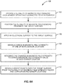
- Figure 6A depicts the steps of a method 100 of analyzing an electrical current over a target surface.
- a plurality of magnetic field sensors 26, preferably arranged in an array 30, is provided (block 102). Each sensor 26 is operatively connected to an integrator 32.
- the plurality of magnetic field sensors 26 is positioned proximate the target surface 18, 24 (block 104), and an electrical current is applied to the target surface 18, 24 (block 106), as depicted in Figure 2 .
- a change in magnetic field strength is sensed at one or more sensor locations 27 (block 108).
- the changes in magnetic field strength are integrated to derive a magnetic field strength value at each sensor location 27 (block 110).
- a current density over the target surface 18, 24 is inferred from the plurality of magnetic field strength values and corresponding sensor locations 27 (block 112).
- Figure 6B depicts, in greater detail, steps taken according to one aspect to implement block 112 of Figure 6A - inferring a current density over the target surface 18, 24 from the plurality of magnetic field strength values and corresponding sensor locations 27. These steps include first inferring a local current value from each magnetic field strength value (block 114), and then mapping the local current values to the target surface 18, 24 using the corresponding sensor locations 27 (block 116).
- Figure 6C depicts the steps of a method 200 of obtaining a higher resolution view of current density over the target surface 18, 24.
- magnetic field strength values are interpolated between sensor locations 27 (block 118).
- Corresponding virtual sensor locations, corresponding to the interpolated magnetic field strength values, are calculated (block 120).
- a local virtual current value is inferred from each interpolated magnetic field strength value (block 122).
- the local virtual current values are then mapped to the target surface 18, 24 using the corresponding virtual sensor locations (block 124).
- Figure 7 depicts a current density plot overlaid on the test structure 10.
- the current density plot results from integrating and post-processing the magnetic field sensor 26 outputs (and optionally interpolating between sensors 26), to infer a current density. As anticipated, current is concentrated in the fasteners 16, but is distributed around them in an unpredictable manner.
- B-dot coils 26 must be calibrated to achieve accurate field measurements. Since the coils 26 tend to be small, physical measurements of the coil area may be inaccurate. Normal manufacturing tolerances will result in coil-to-coil differences in some parameters, such as the number of (partial) turns, the coil surface area, and the like. In addition, non-ideal electronic effects take place, especially involving the self-inductance of the coil 26 or the cabling. Calibration may be accomplished, for example, by applying a known sinusoidal magnetic field, such as from a Helmholtz coil driven by a signal generator, and determining the amplitude of coil response as a function of frequency using an oscilloscope.
- a known sinusoidal magnetic field such as from a Helmholtz coil driven by a signal generator
- Figure 6D depicts the step of a method 300 of calibrating each magnetic field sensor to compensate for individual sensor differences due to manufacturing tolerances (block 126).
- the array 30 holding a plurality of coils 26 must also be calibrated. Referring to Figure 2 , assuming the array 30 of B-dot coils 26 is flat, it is apparent that the coils 26 positioned over the sheet 12 are closer to the surface 18 than the coils 26 positioned over the sheet 14 are to the surface 24, due to the offset of the two sheets 12, 14. Accordingly, all of the coils 26 positioned over the sheet 14 will register a lower intensity magnetic field. This difference in distance of each coil 26 from the target surface 18, 24 must be accounted for in order to obtain an accurate measurement of the magnetic field, from which current over the target surface 18, 24 is inferred.
- an array 30 of magnetic field sensors 26 is calibrated by use of a proxy surface.
- Figure 8 depicts a calibration test structure 50, presenting a proxy surface 52 having the geometry ( e . g ., the shape or form) of a target surface, such as an airplane wing.
- the calibration test structure 50, and hence proxy surface 52 is formed of a dielectric material, and includes one or more conductors 54.
- the conductors 54 are connected to a high voltage source (+HV), and current is directed through the conductors 54, generating magnetic fields around them.
- Figure 9 depicts a cross-section view of the calibration test structure 50, with the section line taken at a conductor 54 lying along, or embedded within, the proxy surface 52.
- Figure 9 also depicts an array 30 of magnetic field sensors 26. As described above with respect to Figure 2 , it is apparent that there are varying distances between different magnetic field sensors 26 and corresponding points on the proxy surface. A calibration procedure is described to compensate for these different distances.
- Figure 6E depicts a method 400 of calibrating a plurality of magnetic field sensors 26 positioned in a fixed array 30.
- the proxy surface 52 is provided, as described above (block 128).
- the proxy surface 52 is formed of a dielectric material, includes one or more conductors 54, and approximates the geometry of a target surface, such as an aircraft wing.
- An array 30 of magnetic field sensors 26 is positioned proximate the proxy surface 52 (block 130), and an electrical current is applied through the conductors 54 (block 132). Note that, as described above, the array 30 of magnetic field sensors 26 extends past the leading edge 56 and trailing edge 58 of the proxy surface 52.
- a plurality of magnetic field sensors 26 each senses a change in magnetic field strength at its respective sensor location 27 (block 134).
- the changes in magnetic field strength are integrated to derive a magnetic field strength value at each sensor location 27 (block 136).
- the outputs of the array 30 of magnetic field sensors 26 are calibrated to compensate for individual sensor 26 differences due to differing geometries between the proxy surface 52 and sensor array 30 (block 138).
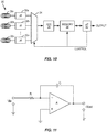
- FIG 10 depicts a simplified view of one aspect of the electronics for an array 30 of magnetic field sensors 26.
- Each magnetic field sensor 26a, 26b, ..., 26n is connected to a corresponding integrator 32a, 32b, ..., 32n.
- Each integrator 32 may comprise an analog circuit, such as an operational amplifier A together with an RC circuit, as depicted in Figure 11 .
- the output of each magnetic field sensor 26 may be digitized, and the integration performed by a Digital Signal Processor (DSP).
- DSP Digital Signal Processor
- the integrators 32 are preferably of high quality, with droop correction and high sensitivity.
- the outputs of the integrators 32 are consecutively (or in any predetermined order) multiplexed by switching unit 34 into an Analog to Digital Converter (ADC) 36.
- ADC Analog to Digital Converter
- the digital data are stored in a non-transitory computer readable medium, such as memory 38 ( e . g ., RAM, ROM, Flash, SSD, HDD, magnetic tape, etc.).
- a controller 40 such as a microprocessor or DSP, then accesses the stored data to perform calibration calculations, calculate the local current values, map the local current values to sensor locations 27, and generate a model or view of the current density over the target surface 18, 24.
- the current density over the target surface 18, 24 may be output, e .
- controller 40 may also control operation of the system components. Those of skill in the art will readily recognize that separate controllers 40 may each perform part of the computational load, such as one controller 40 controlling the system components and another controller 40 calculating current density.
- Technical effects of the systems and methods described herein include at least one of i) providing a plurality of magnetic field sensors, each sensor operatively connected to an integrator; ii) positioning the plurality of magnetic field sensors proximate a target surface; iii) applying an electrical current to the target surface; iv) sensing a change in magnetic field strength at one or more sensor locations; v) integrating the changes in magnetic field strength to derive a magnetic field strength value at each sensor location; and vi) inferring a current density over the target surface from the plurality of magnetic field strength values and corresponding sensor locations.
Landscapes
- Physics & Mathematics (AREA)
- General Physics & Mathematics (AREA)
- Condensed Matter Physics & Semiconductors (AREA)
- Electromagnetism (AREA)
- Engineering & Computer Science (AREA)
- Power Engineering (AREA)
- Measuring Magnetic Variables (AREA)
- Measuring Instrument Details And Bridges, And Automatic Balancing Devices (AREA)
Abstract
Description
- Lightning strikes on aircraft are known to occur. Conventionally, the fuselage and wings of airplanes were made of lightweight metal such as aluminum. Electrical current from lightning generally travels along the outer skin of such airplanes, causing little damage. Conventional airplane metal exteriors exhibit isotropic conductivity, and can carry even large currents in a well-defined and well-understood manner. Testing for lightning survivability is relatively straightforward. The current density over the exterior surface of an airplane in a lightning strike is usually highly uniform. Hence, a local current measured at one spot may reasonably be considered representative of what is occurring over the entire airplane.
- Many modern airplanes are built of composite materials rather than metal. Composites may be lighter and more flexible than metal, with higher elasticity and the ability to embed electronics, such as antennas, into the composite material. Composite airframes are often fabricated in layers. In particular, they may include conductive layers, such as those constructed of carbon fiber, separated by dielectric layers, such as those constructed of various resins. The conductive layers generally exhibit non-isotropic conductivity, such as along the direction of the constituent fibers. Consequently, current density over a composite airframe in a lightning strike is usually non-homogenous, and may be quite complex. This greatly complicates lightning strike research and testing, as it may be difficult to predict or measure current density over the large surface areas.
- The Background section of this document is provided to place aspects of the present invention in technological and operational context, to assist those of skill in the art in understanding their scope and utility. Unless explicitly identified as such, no statement herein is admitted to be prior art merely by its inclusion in the Background section.
- The present invention relates generally to current sensing, and in particular to a method and apparatus for inferring current density over a large surface.
- The following presents a simplified summary of the disclosure in order to provide a basic understanding to those of skill in the art. This summary is not an extensive overview of the disclosure and is not intended to identify key/critical elements of aspects of the invention or to delineate the scope of the invention. The sole purpose of this summary is to present some concepts disclosed herein in a simplified form as a prelude to the more detailed description that is presented later.
- According to one or more aspects described and claimed herein, a plurality of magnetic field sensors, such as arranged in an array, is operative to measure changes in magnetic field strength proximate the surface(s) of a test structure. The test structure may approximate the geometry of an airplane fuselage, wing, or the like. An electric current is applied to the test structure, and the magnetic field sensors sense changes in a magnetic field caused by the current. A corresponding plurality of integrators converts the sensor outputs to magnetic field strength values. From the plurality of magnetic field strength values and corresponding sensor locations, a current density over the target surface is inferred.
- One aspect relates to a method of analyzing an electrical current over a target surface. A plurality of magnetic field sensors is provided. Each sensor is operatively connected to an integrator. The plurality of magnetic field sensors is positioned proximate the target surface. An electrical current is applied to the target surface. A change in magnetic field strength is sensed at one or more sensor locations. The changes in magnetic field strength are integrated to derive a magnetic field strength value at each sensor location. A current density over the target surface is inferred from the plurality of magnetic field strength values and corresponding sensor locations.
- Another aspect relates to an apparatus operative to analyze an electrical current over a target surface. The apparatus includes a plurality of magnetic field sensors positioned at known locations in an array. Each magnetic field sensor is operative to sense a change in magnetic field strength. An integrator is operatively connected to each magnetic field sensor and is operative to derive a magnetic field strength value by integrating the connected sensor's output. A data processing system is operative to receive an output of each integrator, and is further operative to infer a current density over the target surface from the plurality of magnetic field strength values and corresponding sensor locations.
- Yet another aspect relates to a non-transitory computer-readable medium. The medium stores program instructions operative to cause a data processing system to process magnetic field sensor array outputs to analyze an electrical current over a target surface. The instructions cause the data processing system to sense a change in magnetic field strength at one or more sensor locations on the array, when the magnetic field sensor array is positioned proximate the target surface and an electrical current is applied to the target surface; integrate the changes in magnetic field strength to derive a magnetic field strength value at each sensor location; infer a local current value from each magnetic field strength value; and infer a current density over the target surface by mapping the local current values to the target surface using the corresponding sensor locations.
- Also disclosed herein is a non-transitory computer-readable medium storing program instructions operative to cause a data processing system to process magnetic field sensor array outputs to analyze an electrical current over a target surface by performing the steps of: sensing a change in magnetic field strength at one or more sensor locations on the array, when the magnetic field sensor array is positioned proximate the target surface and an electrical current is applied to the target surface; integrating the changes in magnetic field strength to derive a magnetic field strength value at each sensor location; and inferring a local current value from each magnetic field strength value; and inferring a current density over the target surface by mapping the local current values to the target surface using the corresponding sensor locations.
- The program instructions may be operative to cause the data processing system to perform the steps of: interpolating magnetic field strength values between sensor locations; calculating virtual sensor locations corresponding to the interpolated magnetic field strength values; inferring a local virtual current value from each interpolated magnetic field strength value; and generating a high-granularity current density over the target surface by additionally mapping the local virtual current values to the target surface using the corresponding virtual sensor locations.
- The program instructions may be operative to cause the data processing system to calibrate the magnetic field sensor array when the sensor array is positioned proximate a proxy surface formed of a dielectric material, including one or more conductors, and approximating the geometry of the target surface, and current flows through the conductors, by sensing a change in magnetic field strength at one or more sensor locations; integrating the changes in magnetic field strength to derive a magnetic field strength value at each sensor location; and calibrating the array of magnetic field sensors to compensate for individual sensor differences due to geometries of the proxy surface and sensor array.
- The present invention will now be described more fully hereinafter with reference to the accompanying drawings, in which aspects of the invention are shown. However, this invention should not be construed as limited to the aspects set forth herein. Rather, these aspects are provided so that this disclosure will be thorough and complete, and will fully convey the scope of the invention to those skilled in the art. Like numbers refer to like elements throughout.
-
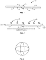
Figure 1 is a section view of a test structure. -
Figure 2 is a section view of magnetic field sensors proximate the test structure. -
Figure 3 is a perspective view of coils in three orthogonal directions. -
Figure 4 is a perspective view of a mounting structure for magnetic field sensors. -
Figure 5 is a perspective view of an array of magnetic field sensors proximate a test structure. -
Figure 6A is a flow diagram of a method of analyzing an electrical current over a target surface. -
Figure 6B is a flow diagram detailing a step of the method ofFigure 6A . -
Figure 6C is a flow diagram of a method of obtaining a higher resolution view of current density over a target surface. -
Figure 6D is a flow diagram of a method of calibrating individual magnetic field sensors. -
Figure 6E is a flow diagram of a method of calibrating an array of magnetic field sensors using a proxy surface. -
Figure 7 is a 2-D plot depicting current density over the test surface. -
Figure 8 is a perspective view of a calibration test structure providing a proxy surface. -
Figure 9 is a section view of the calibration test structure and a sensor array. -
Figure 10 is a block diagram of an electronics system for magnetic field sensors. -
Figure 11 is a schematic diagram of an active integrator circuit. - For simplicity and illustrative purposes, the present invention is described by referring mainly to an exemplary aspect thereof. In the following description, numerous specific details are set forth in order to provide a thorough understanding of the present invention. However, it will be readily apparent to one of ordinary skill in the art that the present invention may be practiced without limitation to these specific details. In this description, well known methods and structures have not been described in detail so as not to unnecessarily obscure the present invention.
- Current density in layered composite materials, including airframes, is non-uniform, and driven by geometry, conductivity, and current magnitude. Small currents may be confined to fiber layers, where the current has a strong preference along the direction of the fibers. Large current may cause destruction by bleeding through layers, as high voltage breaks down the dielectric barriers of insulating resin layers. Consequently, the current density - that is, the concentration of current across the surface of a material - is complex, non-uniform, and difficult to measure.
- Apart from the unique challenges of measuring current density in a composite material, the direct measurement of very large currents itself is usually not possible, due to inductance effects and high energy levels, which can damage measurement equipment. Accordingly, high currents are often inferred by measuring the magnetic fields they generate.
- One current-sensing circuit known in the art (for example, known for measuring current in plasma experiments) is a coil of wire, known in the art as a B-Dot sensor. The name derives from Faraday's equation, which relates voltage induced in a coil to a changing magnetic flux through the coil as

- More precisely, Faraday's law states:

- Although the use of B-dot sensors and concomitant integrator circuits is known to measure magnetic fields, e.g., in studying plasma phenomena (of which lightning strikes are one example), they typically measure current from a single point source. Magnetic sensors have not been used to measure and study current density across a 2-D or 3-D surface.
-
Figure 1 is a side section view of atest structure 10, referred to as a two fastener lap joint, commonly used in Electro-Magnetic Environment (EME) testing. Thetest structure 10 comprises twosheets fasteners 16. The sheet12 has afront side 18, facing up inFigure 1 , and abag side 20 facing down. Thefront side 18 corresponds to the finished, outwardly-facing surface of a composite material on an airplane fuselage or wing. Thebag side 20, so named due to an inflatable bladder used in the fabrication process, corresponds to an interior-facing side. On theother sheet 14, thefront side 22 faces down, and thebag side 24 faces up. Bothsheets test structure 10 when a high current is applied, to simulate a lightning strike. - High voltage is applied to one end of the
test structure 10, such assheet 12, while the other end, such assheet 14, is grounded. This allows current to flow acrosssheet 12, through thefasteners 16, and subsequently acrosssheet 14. It is usually assumed that there would be a 50-50 split in current going through the twofasteners 16. However, some damage assessments imply that this might not be correct. Actually measuring high currents through thefasteners 16 is problematic, and in any event would not yield information about the current density across thesheets -
Figure 2 depicts thetest structure 10 with high voltage (HV) and ground applied, indicating the general direction of current flow I. According to aspects described and claimed herein a plurality ofmagnetic field sensors 26, such as B-dot sensors are positioned proximate to a target surface, such as thefront side surface 18 ofsheet 12 andbag side surface 24 ofsheet 14. Each sensor comprises a coil ofwire 25, and is operatively connected to an integrator (not shown), the outputs of which are collected by a data processing system (not shown). As indicated, an electrical current is applied to the target surfaces 18, 24 of thetest structure 10. Themagnetic field sensors 26 sense a change in magnetic field strength at eachrespective sensor location 27, as the current I ramps up, and possibly changes over thetest structure 10, e.g., in response to temperature changes, voltage-induced damage, or the like. The detected changes in magnetic field strength are integrated to derive a magnetic field strength value at eachsensor location 27. A current density over the target surfaces of thetest structure 10 is then inferred from the plurality of magnetic field strength values andcorresponding sensor locations 27. -
Figure 2 depicts the B-dot coils 26 as being aligned in only a single direction. That is, only onecoil 26 is depicted at eachsensor location 27, and all of thecoils 26 have the same orientation. Eachcoil 26 is operative to detect only changes in a magnetic field whose flux lines are perpendicular to the coil area - that is, the flux lines are parallel with a longitudinal axis extending down the centerline of thecoil 26. For a more complete spatial view of the magnetic field,compound sensors 26 may be constructed, each having multiple coils with different orientations. For example, three coils, arranged about three orthogonal axes, as depicted inFigure 3 , would measure magnetic flux in all three spatial directions (e.g., x, y, and z directions). A composite flux may be obtained as the vector sum of the threecoil 26 outputs. Note that a single coil measures flux in both directions perpendicular to its cross-sectional area - flux in one direction will induce a positive voltage, and flux in the opposite direction will induce a negative voltage. -
Figure 4 depicts a six-pole mounting structure 28 on which six B-dot coils 26 may be wound. In one aspect, providing twocoils 26 in each orientation allows a more robust signal to be obtained as a common mode of a differential pair. In this case, the twocoils 26 in each of the three axes (i.e., directions) should be wound in opposite directions. If the six-pole structure 28 is formed from a nonferrous, dielectric material, it may be left in place to provide structural support for thecoils 26, without impacting the magnetic flux sensing operation. If at least threecoils 26 are mounted at eachstructure 28, e.g., in x, y, and z directions, a resultant magnetic field may be resolved by the vector sum of the magnetic field components detected by each coil 26 (and associated integrator circuit). -
Figure 5 depicts anarray 30 on which a plurality of mountingstructures 28 are affixed to asubstrate 31. Each mountingstructure 28 defines asensor location 27. At least onemagnetic field sensor 26, such as a B-dot coil, is positioned at eachsensor location 27. The plurality ofmagnetic field sensors 26 is positioned proximate to atarget surface test structure 10 inFigure 5 , thetarget surface array 30 and is not visible). In a preferred aspect, thearray 30 ofmagnetic field sensors 26 extends at leastseveral coils 26 past eachrelevant edge 11 of thetest structure 10. This ensures that field behavior at theedges 11 of thetest structure 10 is captured. In particular, by placing B-dot coils 26 past theedges 11 of thetest structure 10, magnetic field behavior at theedges 11 may be derived by interpolation, as described below. In one aspect, one or more indexing features, such as a clip (not shown), ensures repeatability in positioning thearray 30 proximate to atarget surface array 30 placement and orientation, consistent positioning of thearray 30 is still advantageous. -
Figure 6A depicts the steps of amethod 100 of analyzing an electrical current over a target surface. A plurality ofmagnetic field sensors 26, preferably arranged in anarray 30, is provided (block 102). Eachsensor 26 is operatively connected to an integrator 32. The plurality ofmagnetic field sensors 26 is positioned proximate thetarget surface 18, 24 (block 104), and an electrical current is applied to thetarget surface 18, 24 (block 106), as depicted inFigure 2 . A change in magnetic field strength is sensed at one or more sensor locations 27 (block 108). The changes in magnetic field strength are integrated to derive a magnetic field strength value at each sensor location 27 (block 110). A current density over thetarget surface -
Figure 6B depicts, in greater detail, steps taken according to one aspect to implement block 112 ofFigure 6A - inferring a current density over thetarget surface corresponding sensor locations 27. These steps include first inferring a local current value from each magnetic field strength value (block 114), and then mapping the local current values to thetarget surface -
Figure 6C depicts the steps of amethod 200 of obtaining a higher resolution view of current density over thetarget surface target surface -
Figure 7 depicts a current density plot overlaid on thetest structure 10. The current density plot results from integrating and post-processing themagnetic field sensor 26 outputs (and optionally interpolating between sensors 26), to infer a current density. As anticipated, current is concentrated in thefasteners 16, but is distributed around them in an unpredictable manner. - For several reasons, B-
dot coils 26 must be calibrated to achieve accurate field measurements. Since thecoils 26 tend to be small, physical measurements of the coil area may be inaccurate. Normal manufacturing tolerances will result in coil-to-coil differences in some parameters, such as the number of (partial) turns, the coil surface area, and the like. In addition, non-ideal electronic effects take place, especially involving the self-inductance of thecoil 26 or the cabling. Calibration may be accomplished, for example, by applying a known sinusoidal magnetic field, such as from a Helmholtz coil driven by a signal generator, and determining the amplitude of coil response as a function of frequency using an oscilloscope. Alternatively, a network analyzer can be used, which simplifies data collection and allows the phase of the probe's response to be determined as well. Those of skill in the art will recognize that such calibration is routine for measuring equipment, and may devise any number of adequate calibration procedures, given the teachings of the present disclosure.Figure 6D depicts the step of amethod 300 of calibrating each magnetic field sensor to compensate for individual sensor differences due to manufacturing tolerances (block 126). - Apart from calibrating individual B-dot coils 26, the
array 30 holding a plurality ofcoils 26 must also be calibrated. Referring toFigure 2 , assuming thearray 30 of B-dot coils 26 is flat, it is apparent that thecoils 26 positioned over thesheet 12 are closer to thesurface 18 than thecoils 26 positioned over thesheet 14 are to thesurface 24, due to the offset of the twosheets coils 26 positioned over thesheet 14 will register a lower intensity magnetic field. This difference in distance of eachcoil 26 from thetarget surface target surface coil 26 to thetarget surface target surface target surface 
coil 26 from thetarget surface - In one aspect, an
array 30 ofmagnetic field sensors 26 is calibrated by use of a proxy surface.Figure 8 depicts acalibration test structure 50, presenting aproxy surface 52 having the geometry (e.g., the shape or form) of a target surface, such as an airplane wing. Thecalibration test structure 50, and henceproxy surface 52, is formed of a dielectric material, and includes one ormore conductors 54. Theconductors 54 are connected to a high voltage source (+HV), and current is directed through theconductors 54, generating magnetic fields around them. -
Figure 9 depicts a cross-section view of thecalibration test structure 50, with the section line taken at aconductor 54 lying along, or embedded within, theproxy surface 52.Figure 9 also depicts anarray 30 ofmagnetic field sensors 26. As described above with respect toFigure 2 , it is apparent that there are varying distances between differentmagnetic field sensors 26 and corresponding points on the proxy surface. A calibration procedure is described to compensate for these different distances. -
Figure 6E depicts amethod 400 of calibrating a plurality ofmagnetic field sensors 26 positioned in a fixedarray 30. Theproxy surface 52 is provided, as described above (block 128). Theproxy surface 52 is formed of a dielectric material, includes one ormore conductors 54, and approximates the geometry of a target surface, such as an aircraft wing. Anarray 30 ofmagnetic field sensors 26 is positioned proximate the proxy surface 52 (block 130), and an electrical current is applied through the conductors 54 (block 132). Note that, as described above, thearray 30 ofmagnetic field sensors 26 extends past the leadingedge 56 and trailingedge 58 of theproxy surface 52. A plurality ofmagnetic field sensors 26 each senses a change in magnetic field strength at its respective sensor location 27 (block 134). The changes in magnetic field strength are integrated to derive a magnetic field strength value at each sensor location 27 (block 136). The outputs of thearray 30 ofmagnetic field sensors 26 are calibrated to compensate forindividual sensor 26 differences due to differing geometries between theproxy surface 52 and sensor array 30 (block 138). -
Figure 10 depicts a simplified view of one aspect of the electronics for anarray 30 ofmagnetic field sensors 26. Eachmagnetic field sensor corresponding integrator Figure 11 . Alternatively, the output of eachmagnetic field sensor 26 may be digitized, and the integration performed by a Digital Signal Processor (DSP). In either case, the integrators 32 are preferably of high quality, with droop correction and high sensitivity. In the representative system ofFigure 8 , the outputs of the integrators 32 are consecutively (or in any predetermined order) multiplexed by switchingunit 34 into an Analog to Digital Converter (ADC) 36. The digital data are stored in a non-transitory computer readable medium, such as memory 38 (e.g., RAM, ROM, Flash, SSD, HDD, magnetic tape, etc.). Acontroller 40, such as a microprocessor or DSP, then accesses the stored data to perform calibration calculations, calculate the local current values, map the local current values tosensor locations 27, and generate a model or view of the current density over thetarget surface target surface controller 40 may also control operation of the system components. Those of skill in the art will readily recognize thatseparate controllers 40 may each perform part of the computational load, such as onecontroller 40 controlling the system components and anothercontroller 40 calculating current density. - Technical effects of the systems and methods described herein include at least one of i) providing a plurality of magnetic field sensors, each sensor operatively connected to an integrator; ii) positioning the plurality of magnetic field sensors proximate a target surface; iii) applying an electrical current to the target surface; iv) sensing a change in magnetic field strength at one or more sensor locations; v) integrating the changes in magnetic field strength to derive a magnetic field strength value at each sensor location; and vi) inferring a current density over the target surface from the plurality of magnetic field strength values and corresponding sensor locations.
- Aspects of the present invention provide numerous advantages over the prior art. There is currently no way to accurately measure real-world current over large surfaces. The need for this ability is particularly acute, for example to model and study the effects of lightning strikes, as aircraft wings and fuselages evolve from metal to composite construction.
- The present invention may, of course, be carried out in other ways than those specifically set forth herein without departing from essential characteristics of the invention. The present aspects are to be considered in all respects as illustrative and not restrictive, and all changes coming within the meaning and equivalency range of the appended claims are intended to be embraced therein.
Claims (15)
- A method (100) of analyzing an electrical current over a target surface (18, 24), comprising:providing (102) a plurality of magnetic field sensors (26), each sensor operatively connected to an integrator (32);positioning (104) the plurality of magnetic field sensors proximate the target surface;applying (106) an electrical current to the target surface;sensing (108) a change in magnetic field strength at one or more sensor locations (27);integrating (110) the changes in magnetic field strength to derive a magnetic field strength value at each sensor location; andinferring (112) a current density over the target surface from the plurality of magnetic field strength values and corresponding sensor locations.
- The method of claim 1 wherein inferring a current density over the target surface comprises inferring (114) a local current value from each magnetic field strength value, and mapping (116) the local current values to the target surface using the corresponding sensor locations.
- The method of claim 1 or claim 2 comprising
interpolating (118) magnetic field strength values between sensor locations;
calculating (120) virtual sensor locations corresponding to the interpolated magnetic field strength values;
inferring (122) a local virtual current value from each interpolated magnetic field strength value; and
mapping (124) the local virtual current values to the target surface using the corresponding virtual sensor locations. - The method according to any preceding claim comprising, prior to sensing a change in magnetic field strength at one or more sensor locations, calibrating (126) each magnetic field sensor to compensate for individual sensor differences due to manufacturing tolerances,
wherein the magnetic field sensors each optionally comprise a wire coil (25), and
wherein the manufacturing tolerances optionally include at least one of the type of wire in the coil, the number of turns of wire in the coil, and the area of the coil. - The method according to any of claims 1 to 3 wherein the plurality of magnetic field sensors is positioned in a fixed array (30), the method comprising, prior to sensing a change in magnetic field strength at one or more sensor locations, calibrating the plurality of magnetic field sensors by:providing (128) a proxy surface (52), formed of a dielectric material and including one or more conductors (54), the proxy surface approximating the geometry of the target surface;positioning (130) the array of magnetic field sensors proximate the proxy surface;applying (132) an electrical current through the conductors of the proxy surface;sensing (134) a change in magnetic field strength at one or more sensor locations;integrating (136) the changes in magnetic field strength to derive a magnetic field strength value at each sensor location; andcalibrating (138) the array of magnetic field sensors to compensate for individual sensor differences due to geometries of the proxy surface and sensor array.
- The method according to any preceding claim wherein one or more magnetic field sensors comprise two or more wire coils oriented to sense changes in magnetic field strength in different directions, and wherein deriving a magnetic field strength value at each sensor location further comprises deriving a resultant magnetic field strength and direction for each magnetic field sensor by combining magnetic field strength values of the two or more wire coils and the wire coil orientations.
- The method of claim 6, wherein the wire coil orientation directions are orthogonal to each other, and
wherein one or more magnetic field sensors optionally comprise three wire coils (25) oriented to sense changes in magnetic field strength in three orthogonal directions. - The method according to any of claims 1 to 5 wherein one or more magnetic field sensors comprise two wire coils (25) oriented along the same direction but oppositely wound, and wherein deriving a magnetic field strength value at each sensor location comprises deriving the magnetic field strength from a common mode of the two wire coils, wherein extraneous magnetic fields are rejected.
- An apparatus operative to analyze an electrical current over a target surface (18, 24), comprising:a plurality of magnetic field sensors (26) positioned at known locations (27) in an array (30), each magnetic field sensor operative to sense a change in magnetic field strength;an integrator (32) operatively connected to each magnetic field sensor and operative to derive a magnetic field strength value by integrating the connected sensor's output; anda data processing system (40) operative to receive an output of each integrator, and further operative to infer a current density over the target surface from the plurality of magnetic field strength values and corresponding sensor locations.
- The apparatus of claim 9 wherein one or more magnetic field sensors comprise two or more wire coils oriented to sense changes in magnetic field strength in different directions, and wherein the data processing system is further operative to derive a resultant magnetic field strength and direction for each magnetic field sensor by combining magnetic field strength values of the two or more wire coils and the wire coil orientations.
- The apparatus of claim 10 wherein the wire coil orientation directions are orthogonal to each other.
- The apparatus of claim 10 or claim 11 wherein one or more magnetic field sensors comprise three wire coils (25) oriented to sense changes in magnetic field strength in three orthogonal directions.
- The apparatus according to any of claims 10 to 12 wherein the array of magnetic field sensors comprises:a substrate (31); anda plurality of mounting members (28) affixed to the substrate at the known magnetic field sensor locations, each mounting member comprising at least two extension members on which wire coils are wound to form magnetic field sensors,wherein the plurality of mounting members are affixed to the substrate such that corresponding extension members are oriented in the same direction.
- The apparatus of claim 13 wherein the extension members comprise corresponding pairs of extension members oriented 180° apart; the pairs of coils are wound in opposite directions on each extension member of a pair, the integrator is further operative to derive a magnetic field strength value at each sensor location from a common mode of each pair of wire coils, and wherein extraneous magnetic fields are rejected.
- The apparatus of any of claims 9 to 14 wherein the array is sufficiently larger than the target surface that when the array is positioned proximate the target surface, a subset of magnetic field sensors are positioned beyond the outer edges (11) of the target surface.
Applications Claiming Priority (1)
| Application Number | Priority Date | Filing Date | Title |
|---|---|---|---|
| US15/671,004 US10677612B2 (en) | 2017-08-07 | 2017-08-07 | Large surface magnetic field sensor array |
Publications (2)
| Publication Number | Publication Date |
|---|---|
| EP3441774A1 true EP3441774A1 (en) | 2019-02-13 |
| EP3441774B1 EP3441774B1 (en) | 2022-07-27 |
Family
ID=63404941
Family Applications (1)
| Application Number | Title | Priority Date | Filing Date |
|---|---|---|---|
| EP18187700.2A Active EP3441774B1 (en) | 2017-08-07 | 2018-08-07 | Large surface magnetic field sensor array and method of analysing an electrical current over a surface |
Country Status (6)
| Country | Link |
|---|---|
| US (1) | US10677612B2 (en) |
| EP (1) | EP3441774B1 (en) |
| JP (1) | JP7290402B2 (en) |
| KR (1) | KR102537765B1 (en) |
| CN (1) | CN109387707B (en) |
| CA (1) | CA3001834C (en) |
Families Citing this family (7)
| Publication number | Priority date | Publication date | Assignee | Title |
|---|---|---|---|---|
| DE102019113219A1 (en) * | 2019-05-20 | 2020-11-26 | Deutsche Post Ag | Sensor device for recognizing successive objects |
| CN112394243B (en) * | 2019-08-19 | 2024-11-08 | 广东美的白色家电技术创新中心有限公司 | Detection modules and electrical equipment |
| CN111273202A (en) * | 2020-02-25 | 2020-06-12 | 中国电子科技集团公司第二十九研究所 | Array-based magnetic sensor compensation method |
| CN112130003B (en) * | 2020-09-03 | 2021-11-09 | 南京理工大学 | Device and method for removing electromagnetic interference signals in same frequency band |
| CN115932980B (en) * | 2022-12-14 | 2025-08-15 | 西北核技术研究所 | Manufacturing method of differential current detector |
| US12385764B2 (en) * | 2022-12-30 | 2025-08-12 | Mitutoyo Corporation | Absolute position encoder utilizing single track configuration |
| JP2025112668A (en) * | 2024-01-19 | 2025-08-01 | 株式会社Subaru | Sensor Positioning Method |
Citations (2)
| Publication number | Priority date | Publication date | Assignee | Title |
|---|---|---|---|---|
| US20060066304A1 (en) * | 2004-08-27 | 2006-03-30 | The Board of Regents University | Electric/magnetic field sensor |
| US20160077027A1 (en) * | 2011-04-12 | 2016-03-17 | The Boeing Company | Utilization of aircraft bondline embedded current sensors in the determination of a lightning damage index |
Family Cites Families (18)
| Publication number | Priority date | Publication date | Assignee | Title |
|---|---|---|---|---|
| JPH07104403B2 (en) * | 1990-09-07 | 1995-11-13 | ダイキン工業株式会社 | Magnetic field measuring method and apparatus thereof |
| JPH0542119A (en) * | 1991-08-12 | 1993-02-23 | Fujitsu Ltd | Biomagnetism measuring instrument |
| JP2782316B2 (en) * | 1993-12-09 | 1998-07-30 | 東北リコー株式会社 | Leakage magnetic flux detection device and switching power supply device |
| JP3303650B2 (en) * | 1996-02-20 | 2002-07-22 | 日本鋼管株式会社 | Calibration method of magnetic sensor array |
| JPH1114671A (en) * | 1997-06-23 | 1999-01-22 | Nec Corp | Current-estimating device |
| JP3757815B2 (en) * | 2001-04-27 | 2006-03-22 | 株式会社日立製作所 | Biomagnetic field measurement device |
| JP2004069357A (en) * | 2002-08-02 | 2004-03-04 | Nec Tokin Corp | 3 stem magnetometric sensor and array type magnetometric sensor |
| JP2005003503A (en) * | 2003-06-11 | 2005-01-06 | Foresutekku:Kk | Magnetic-shielding method using induction coil |
| US6924644B2 (en) * | 2003-09-12 | 2005-08-02 | The United States Of America As Represented By The Secretary Of The Navy | Radiofrequency surface detection coil |
| CN1957257A (en) * | 2004-05-24 | 2007-05-02 | 皇家飞利浦电子股份有限公司 | Magneto-resistive sensor for high sensitivity depth probing |
| US8058865B2 (en) * | 2005-08-30 | 2011-11-15 | Nctengineering Gmbh | Sensor device, sensor arrangement, and method of measuring a property of an object |
| CA2711956A1 (en) * | 2008-01-17 | 2009-07-23 | The Regents Of The University Of California | Integrated magnetic field generation and detection platform |
| CN101839938A (en) * | 2010-04-15 | 2010-09-22 | 西安爱邦电磁技术有限责任公司 | Method for testing airplane model lightning current distribution by utilizing thermal infrared imager |
| JP2011232063A (en) * | 2010-04-26 | 2011-11-17 | Jfe Steel Corp | Method and device for measuring potential distribution of metal plate |
| CN102426310B (en) * | 2011-10-09 | 2014-03-19 | 中国航空无线电电子研究所 | Novel full aircraft high-strength irradiation test method |
| CN103439532B (en) * | 2013-09-02 | 2016-04-13 | 厦门乐钢材料科技有限公司 | A kind of Technology of Microelectrodes in situ detection metal surface microcell distribution of current |
| JP6296843B2 (en) * | 2014-03-13 | 2018-03-20 | 株式会社東芝 | Paper sheet processing equipment |
| CN106093537B (en) * | 2016-07-26 | 2019-02-15 | 河北大学 | Device and method for real-time current density measurement on surface of rotating roller of high-voltage electrostatic separator |
-
2017
- 2017-08-07 US US15/671,004 patent/US10677612B2/en active Active
-
2018
- 2018-04-16 CA CA3001834A patent/CA3001834C/en active Active
- 2018-04-27 KR KR1020180049045A patent/KR102537765B1/en active Active
- 2018-05-23 CN CN201810500300.4A patent/CN109387707B/en active Active
- 2018-08-06 JP JP2018147321A patent/JP7290402B2/en active Active
- 2018-08-07 EP EP18187700.2A patent/EP3441774B1/en active Active
Patent Citations (2)
| Publication number | Priority date | Publication date | Assignee | Title |
|---|---|---|---|---|
| US20060066304A1 (en) * | 2004-08-27 | 2006-03-30 | The Board of Regents University | Electric/magnetic field sensor |
| US20160077027A1 (en) * | 2011-04-12 | 2016-03-17 | The Boeing Company | Utilization of aircraft bondline embedded current sensors in the determination of a lightning damage index |
Also Published As
| Publication number | Publication date |
|---|---|
| US10677612B2 (en) | 2020-06-09 |
| CA3001834C (en) | 2023-06-27 |
| CN109387707A (en) | 2019-02-26 |
| KR102537765B1 (en) | 2023-05-26 |
| CN109387707B (en) | 2022-07-08 |
| EP3441774B1 (en) | 2022-07-27 |
| JP2019066460A (en) | 2019-04-25 |
| CA3001834A1 (en) | 2019-02-07 |
| US20190041236A1 (en) | 2019-02-07 |
| KR20190015984A (en) | 2019-02-15 |
| JP7290402B2 (en) | 2023-06-13 |
Similar Documents
| Publication | Publication Date | Title |
|---|---|---|
| EP3441774B1 (en) | Large surface magnetic field sensor array and method of analysing an electrical current over a surface | |
| CN112611911B (en) | Method, system and sensor for determining position of magnetic field detection component of current sensor | |
| EP0950900B1 (en) | Electromagnetic wave source probing device and method with the probing device | |
| CN106940343A (en) | A kind of material micro-damage detection method and system based on array electromagnetic sensor | |
| US20180292469A1 (en) | Method and arrangement for determining the transverse sensitivity of magnetic field sensors | |
| CA2833330C (en) | System and method for measuring wrinkle depth in a composite structure | |
| EP3084417B1 (en) | Structural health monitoring system employing electromechanical impedance technology | |
| US7511485B2 (en) | Magnetic field measurement method and system | |
| US7417424B2 (en) | Magnetic-field-measuring device | |
| Wang et al. | Research on synchronous measurement methods based on non-contact sensing | |
| CA3095712A1 (en) | Method for non-destructive inspection of anodes for aluminium reduction cells | |
| US9494622B2 (en) | Current measurement device and current measurement method | |
| EP3431981B1 (en) | Method for inspecting electroconductive composite material and device for inspecting electroconductive composite material | |
| van Deursen et al. | Inductive sensor for lightning current measurement, fitted in aircraft windows—Part I: Analysis for a circular window | |
| CN114778949A (en) | Ground grid grounding resistance detection auxiliary method based on unmanned aerial vehicle | |
| CN113156349A (en) | Method and device for measuring magneto-mechanical properties of material | |
| JP5170955B2 (en) | Electromagnetic wave measuring method and electromagnetic wave measuring device | |
| Somsak et al. | Conductive microbead array detection based on eddy-current testing using SV-GMR sensor and Helmholtz coil exciter | |
| CA2754181C (en) | Environmental damage sensor | |
| EP4686947A1 (en) | Systems and methods for estimating a speed of a vehicle | |
| WO2021111346A1 (en) | System and method for measuring a deformation of a structure of an aircraft | |
| Pereles et al. | A wireless, magnetoelastic-based sensor array for force monitoring on a hard surface | |
| CN104049228A (en) | Magnetic sensor dynamic model calibration method | |
| Reinbacher-Köstinger et al. | Fast, accurate and reliable identification of hidden conductive objects with deterministic and stochastic methods | |
| Zhou et al. | Calibration Of Air-Core Sensor By Braunbeck Coil |
Legal Events
| Date | Code | Title | Description |
|---|---|---|---|
| PUAI | Public reference made under article 153(3) epc to a published international application that has entered the european phase |
Free format text: ORIGINAL CODE: 0009012 |
|
| STAA | Information on the status of an ep patent application or granted ep patent |
Free format text: STATUS: REQUEST FOR EXAMINATION WAS MADE |
|
| 17P | Request for examination filed |
Effective date: 20180807 |
|
| AK | Designated contracting states |
Kind code of ref document: A1 Designated state(s): AL AT BE BG CH CY CZ DE DK EE ES FI FR GB GR HR HU IE IS IT LI LT LU LV MC MK MT NL NO PL PT RO RS SE SI SK SM TR |
|
| AX | Request for extension of the european patent |
Extension state: BA ME |
|
| GRAP | Despatch of communication of intention to grant a patent |
Free format text: ORIGINAL CODE: EPIDOSNIGR1 |
|
| STAA | Information on the status of an ep patent application or granted ep patent |
Free format text: STATUS: GRANT OF PATENT IS INTENDED |
|
| INTG | Intention to grant announced |
Effective date: 20220217 |
|
| GRAS | Grant fee paid |
Free format text: ORIGINAL CODE: EPIDOSNIGR3 |
|
| GRAA | (expected) grant |
Free format text: ORIGINAL CODE: 0009210 |
|
| STAA | Information on the status of an ep patent application or granted ep patent |
Free format text: STATUS: THE PATENT HAS BEEN GRANTED |
|
| AK | Designated contracting states |
Kind code of ref document: B1 Designated state(s): AL AT BE BG CH CY CZ DE DK EE ES FI FR GB GR HR HU IE IS IT LI LT LU LV MC MK MT NL NO PL PT RO RS SE SI SK SM TR |
|
| REG | Reference to a national code |
Ref country code: CH Ref legal event code: EP |
|
| REG | Reference to a national code |
Ref country code: AT Ref legal event code: REF Ref document number: 1507402 Country of ref document: AT Kind code of ref document: T Effective date: 20220815 |
|
| REG | Reference to a national code |
Ref country code: DE Ref legal event code: R096 Ref document number: 602018038370 Country of ref document: DE |
|
| REG | Reference to a national code |
Ref country code: IE Ref legal event code: FG4D |
|
| REG | Reference to a national code |
Ref country code: LT Ref legal event code: MG9D |
|
| REG | Reference to a national code |
Ref country code: NL Ref legal event code: MP Effective date: 20220727 |
|
| PG25 | Lapsed in a contracting state [announced via postgrant information from national office to epo] |
Ref country code: SE Free format text: LAPSE BECAUSE OF FAILURE TO SUBMIT A TRANSLATION OF THE DESCRIPTION OR TO PAY THE FEE WITHIN THE PRESCRIBED TIME-LIMIT Effective date: 20220727 Ref country code: RS Free format text: LAPSE BECAUSE OF FAILURE TO SUBMIT A TRANSLATION OF THE DESCRIPTION OR TO PAY THE FEE WITHIN THE PRESCRIBED TIME-LIMIT Effective date: 20220727 Ref country code: PT Free format text: LAPSE BECAUSE OF FAILURE TO SUBMIT A TRANSLATION OF THE DESCRIPTION OR TO PAY THE FEE WITHIN THE PRESCRIBED TIME-LIMIT Effective date: 20221128 Ref country code: NO Free format text: LAPSE BECAUSE OF FAILURE TO SUBMIT A TRANSLATION OF THE DESCRIPTION OR TO PAY THE FEE WITHIN THE PRESCRIBED TIME-LIMIT Effective date: 20221027 Ref country code: NL Free format text: LAPSE BECAUSE OF FAILURE TO SUBMIT A TRANSLATION OF THE DESCRIPTION OR TO PAY THE FEE WITHIN THE PRESCRIBED TIME-LIMIT Effective date: 20220727 Ref country code: LV Free format text: LAPSE BECAUSE OF FAILURE TO SUBMIT A TRANSLATION OF THE DESCRIPTION OR TO PAY THE FEE WITHIN THE PRESCRIBED TIME-LIMIT Effective date: 20220727 Ref country code: LT Free format text: LAPSE BECAUSE OF FAILURE TO SUBMIT A TRANSLATION OF THE DESCRIPTION OR TO PAY THE FEE WITHIN THE PRESCRIBED TIME-LIMIT Effective date: 20220727 Ref country code: FI Free format text: LAPSE BECAUSE OF FAILURE TO SUBMIT A TRANSLATION OF THE DESCRIPTION OR TO PAY THE FEE WITHIN THE PRESCRIBED TIME-LIMIT Effective date: 20220727 Ref country code: ES Free format text: LAPSE BECAUSE OF FAILURE TO SUBMIT A TRANSLATION OF THE DESCRIPTION OR TO PAY THE FEE WITHIN THE PRESCRIBED TIME-LIMIT Effective date: 20220727 |
|
| REG | Reference to a national code |
Ref country code: AT Ref legal event code: MK05 Ref document number: 1507402 Country of ref document: AT Kind code of ref document: T Effective date: 20220727 |
|
| PG25 | Lapsed in a contracting state [announced via postgrant information from national office to epo] |
Ref country code: PL Free format text: LAPSE BECAUSE OF FAILURE TO SUBMIT A TRANSLATION OF THE DESCRIPTION OR TO PAY THE FEE WITHIN THE PRESCRIBED TIME-LIMIT Effective date: 20220727 Ref country code: IS Free format text: LAPSE BECAUSE OF FAILURE TO SUBMIT A TRANSLATION OF THE DESCRIPTION OR TO PAY THE FEE WITHIN THE PRESCRIBED TIME-LIMIT Effective date: 20221127 Ref country code: HR Free format text: LAPSE BECAUSE OF FAILURE TO SUBMIT A TRANSLATION OF THE DESCRIPTION OR TO PAY THE FEE WITHIN THE PRESCRIBED TIME-LIMIT Effective date: 20220727 Ref country code: GR Free format text: LAPSE BECAUSE OF FAILURE TO SUBMIT A TRANSLATION OF THE DESCRIPTION OR TO PAY THE FEE WITHIN THE PRESCRIBED TIME-LIMIT Effective date: 20221028 |
|
| RAP4 | Party data changed (patent owner data changed or rights of a patent transferred) |
Owner name: THE BOEING COMPANY |
|
| REG | Reference to a national code |
Ref country code: CH Ref legal event code: PL |
|
| PG25 | Lapsed in a contracting state [announced via postgrant information from national office to epo] |
Ref country code: SM Free format text: LAPSE BECAUSE OF FAILURE TO SUBMIT A TRANSLATION OF THE DESCRIPTION OR TO PAY THE FEE WITHIN THE PRESCRIBED TIME-LIMIT Effective date: 20220727 Ref country code: RO Free format text: LAPSE BECAUSE OF FAILURE TO SUBMIT A TRANSLATION OF THE DESCRIPTION OR TO PAY THE FEE WITHIN THE PRESCRIBED TIME-LIMIT Effective date: 20220727 Ref country code: MC Free format text: LAPSE BECAUSE OF FAILURE TO SUBMIT A TRANSLATION OF THE DESCRIPTION OR TO PAY THE FEE WITHIN THE PRESCRIBED TIME-LIMIT Effective date: 20220727 Ref country code: LU Free format text: LAPSE BECAUSE OF NON-PAYMENT OF DUE FEES Effective date: 20220807 Ref country code: LI Free format text: LAPSE BECAUSE OF NON-PAYMENT OF DUE FEES Effective date: 20220831 Ref country code: DK Free format text: LAPSE BECAUSE OF FAILURE TO SUBMIT A TRANSLATION OF THE DESCRIPTION OR TO PAY THE FEE WITHIN THE PRESCRIBED TIME-LIMIT Effective date: 20220727 Ref country code: CZ Free format text: LAPSE BECAUSE OF FAILURE TO SUBMIT A TRANSLATION OF THE DESCRIPTION OR TO PAY THE FEE WITHIN THE PRESCRIBED TIME-LIMIT Effective date: 20220727 Ref country code: CH Free format text: LAPSE BECAUSE OF NON-PAYMENT OF DUE FEES Effective date: 20220831 Ref country code: AT Free format text: LAPSE BECAUSE OF FAILURE TO SUBMIT A TRANSLATION OF THE DESCRIPTION OR TO PAY THE FEE WITHIN THE PRESCRIBED TIME-LIMIT Effective date: 20220727 |
|
| REG | Reference to a national code |
Ref country code: DE Ref legal event code: R097 Ref document number: 602018038370 Country of ref document: DE Ref country code: BE Ref legal event code: MM Effective date: 20220831 |
|
| PG25 | Lapsed in a contracting state [announced via postgrant information from national office to epo] |
Ref country code: SK Free format text: LAPSE BECAUSE OF FAILURE TO SUBMIT A TRANSLATION OF THE DESCRIPTION OR TO PAY THE FEE WITHIN THE PRESCRIBED TIME-LIMIT Effective date: 20220727 Ref country code: EE Free format text: LAPSE BECAUSE OF FAILURE TO SUBMIT A TRANSLATION OF THE DESCRIPTION OR TO PAY THE FEE WITHIN THE PRESCRIBED TIME-LIMIT Effective date: 20220727 |
|
| PLBE | No opposition filed within time limit |
Free format text: ORIGINAL CODE: 0009261 |
|
| STAA | Information on the status of an ep patent application or granted ep patent |
Free format text: STATUS: NO OPPOSITION FILED WITHIN TIME LIMIT |
|
| P01 | Opt-out of the competence of the unified patent court (upc) registered |
Effective date: 20230516 |
|
| PG25 | Lapsed in a contracting state [announced via postgrant information from national office to epo] |
Ref country code: AL Free format text: LAPSE BECAUSE OF FAILURE TO SUBMIT A TRANSLATION OF THE DESCRIPTION OR TO PAY THE FEE WITHIN THE PRESCRIBED TIME-LIMIT Effective date: 20220727 |
|
| 26N | No opposition filed |
Effective date: 20230502 |
|
| PG25 | Lapsed in a contracting state [announced via postgrant information from national office to epo] |
Ref country code: IE Free format text: LAPSE BECAUSE OF NON-PAYMENT OF DUE FEES Effective date: 20220807 |
|
| PG25 | Lapsed in a contracting state [announced via postgrant information from national office to epo] |
Ref country code: SI Free format text: LAPSE BECAUSE OF FAILURE TO SUBMIT A TRANSLATION OF THE DESCRIPTION OR TO PAY THE FEE WITHIN THE PRESCRIBED TIME-LIMIT Effective date: 20220727 |
|
| PG25 | Lapsed in a contracting state [announced via postgrant information from national office to epo] |
Ref country code: BE Free format text: LAPSE BECAUSE OF NON-PAYMENT OF DUE FEES Effective date: 20220831 |
|
| PG25 | Lapsed in a contracting state [announced via postgrant information from national office to epo] |
Ref country code: HU Free format text: LAPSE BECAUSE OF FAILURE TO SUBMIT A TRANSLATION OF THE DESCRIPTION OR TO PAY THE FEE WITHIN THE PRESCRIBED TIME-LIMIT; INVALID AB INITIO Effective date: 20180807 |
|
| PG25 | Lapsed in a contracting state [announced via postgrant information from national office to epo] |
Ref country code: CY Free format text: LAPSE BECAUSE OF FAILURE TO SUBMIT A TRANSLATION OF THE DESCRIPTION OR TO PAY THE FEE WITHIN THE PRESCRIBED TIME-LIMIT Effective date: 20220727 |
|
| PG25 | Lapsed in a contracting state [announced via postgrant information from national office to epo] |
Ref country code: MK Free format text: LAPSE BECAUSE OF FAILURE TO SUBMIT A TRANSLATION OF THE DESCRIPTION OR TO PAY THE FEE WITHIN THE PRESCRIBED TIME-LIMIT Effective date: 20220727 Ref country code: IT Free format text: LAPSE BECAUSE OF FAILURE TO SUBMIT A TRANSLATION OF THE DESCRIPTION OR TO PAY THE FEE WITHIN THE PRESCRIBED TIME-LIMIT Effective date: 20220727 |
|
| PG25 | Lapsed in a contracting state [announced via postgrant information from national office to epo] |
Ref country code: TR Free format text: LAPSE BECAUSE OF FAILURE TO SUBMIT A TRANSLATION OF THE DESCRIPTION OR TO PAY THE FEE WITHIN THE PRESCRIBED TIME-LIMIT Effective date: 20220727 |
|
| PG25 | Lapsed in a contracting state [announced via postgrant information from national office to epo] |
Ref country code: BG Free format text: LAPSE BECAUSE OF FAILURE TO SUBMIT A TRANSLATION OF THE DESCRIPTION OR TO PAY THE FEE WITHIN THE PRESCRIBED TIME-LIMIT Effective date: 20220727 |
|
| PG25 | Lapsed in a contracting state [announced via postgrant information from national office to epo] |
Ref country code: MT Free format text: LAPSE BECAUSE OF FAILURE TO SUBMIT A TRANSLATION OF THE DESCRIPTION OR TO PAY THE FEE WITHIN THE PRESCRIBED TIME-LIMIT Effective date: 20220727 |
|
| PGFP | Annual fee paid to national office [announced via postgrant information from national office to epo] |
Ref country code: DE Payment date: 20250827 Year of fee payment: 8 |
|
| PGFP | Annual fee paid to national office [announced via postgrant information from national office to epo] |
Ref country code: GB Payment date: 20250827 Year of fee payment: 8 |
|
| PGFP | Annual fee paid to national office [announced via postgrant information from national office to epo] |
Ref country code: FR Payment date: 20250825 Year of fee payment: 8 |