EP3439447A1 - Electromagnetic-wave shield film - Google Patents
Electromagnetic-wave shield film Download PDFInfo
- Publication number
- EP3439447A1 EP3439447A1 EP17773845.7A EP17773845A EP3439447A1 EP 3439447 A1 EP3439447 A1 EP 3439447A1 EP 17773845 A EP17773845 A EP 17773845A EP 3439447 A1 EP3439447 A1 EP 3439447A1
- Authority
- EP
- European Patent Office
- Prior art keywords
- electromagnetic wave
- wave shielding
- shielding film
- conductive
- conductive layer
- Prior art date
- Legal status (The legal status is an assumption and is not a legal conclusion. Google has not performed a legal analysis and makes no representation as to the accuracy of the status listed.)
- Pending
Links
Images


Classifications
-
- H—ELECTRICITY
- H05—ELECTRIC TECHNIQUES NOT OTHERWISE PROVIDED FOR
- H05K—PRINTED CIRCUITS; CASINGS OR CONSTRUCTIONAL DETAILS OF ELECTRIC APPARATUS; MANUFACTURE OF ASSEMBLAGES OF ELECTRICAL COMPONENTS
- H05K9/00—Screening of apparatus or components against electric or magnetic fields
- H05K9/0073—Shielding materials
- H05K9/0081—Electromagnetic shielding materials, e.g. EMI, RFI shielding
- H05K9/0083—Electromagnetic shielding materials, e.g. EMI, RFI shielding comprising electro-conductive non-fibrous particles embedded in an electrically insulating supporting structure, e.g. powder, flakes, whiskers
-
- B—PERFORMING OPERATIONS; TRANSPORTING
- B32—LAYERED PRODUCTS
- B32B—LAYERED PRODUCTS, i.e. PRODUCTS BUILT-UP OF STRATA OF FLAT OR NON-FLAT, e.g. CELLULAR OR HONEYCOMB, FORM
- B32B27/00—Layered products comprising a layer of synthetic resin
- B32B27/18—Layered products comprising a layer of synthetic resin characterised by the use of special additives
-
- C—CHEMISTRY; METALLURGY
- C09—DYES; PAINTS; POLISHES; NATURAL RESINS; ADHESIVES; COMPOSITIONS NOT OTHERWISE PROVIDED FOR; APPLICATIONS OF MATERIALS NOT OTHERWISE PROVIDED FOR
- C09D—COATING COMPOSITIONS, e.g. PAINTS, VARNISHES OR LACQUERS; FILLING PASTES; CHEMICAL PAINT OR INK REMOVERS; INKS; CORRECTING FLUIDS; WOODSTAINS; PASTES OR SOLIDS FOR COLOURING OR PRINTING; USE OF MATERIALS THEREFOR
- C09D5/00—Coating compositions, e.g. paints, varnishes or lacquers, characterised by their physical nature or the effects produced; Filling pastes
- C09D5/24—Electrically-conducting paints
-
- C—CHEMISTRY; METALLURGY
- C09—DYES; PAINTS; POLISHES; NATURAL RESINS; ADHESIVES; COMPOSITIONS NOT OTHERWISE PROVIDED FOR; APPLICATIONS OF MATERIALS NOT OTHERWISE PROVIDED FOR
- C09D—COATING COMPOSITIONS, e.g. PAINTS, VARNISHES OR LACQUERS; FILLING PASTES; CHEMICAL PAINT OR INK REMOVERS; INKS; CORRECTING FLUIDS; WOODSTAINS; PASTES OR SOLIDS FOR COLOURING OR PRINTING; USE OF MATERIALS THEREFOR
- C09D7/00—Features of coating compositions, not provided for in group C09D5/00; Processes for incorporating ingredients in coating compositions
- C09D7/40—Additives
- C09D7/60—Additives non-macromolecular
- C09D7/61—Additives non-macromolecular inorganic
-
- C—CHEMISTRY; METALLURGY
- C09—DYES; PAINTS; POLISHES; NATURAL RESINS; ADHESIVES; COMPOSITIONS NOT OTHERWISE PROVIDED FOR; APPLICATIONS OF MATERIALS NOT OTHERWISE PROVIDED FOR
- C09D—COATING COMPOSITIONS, e.g. PAINTS, VARNISHES OR LACQUERS; FILLING PASTES; CHEMICAL PAINT OR INK REMOVERS; INKS; CORRECTING FLUIDS; WOODSTAINS; PASTES OR SOLIDS FOR COLOURING OR PRINTING; USE OF MATERIALS THEREFOR
- C09D7/00—Features of coating compositions, not provided for in group C09D5/00; Processes for incorporating ingredients in coating compositions
- C09D7/40—Additives
- C09D7/66—Additives characterised by particle size
- C09D7/69—Particle size larger than 1000 nm
-
- H—ELECTRICITY
- H05—ELECTRIC TECHNIQUES NOT OTHERWISE PROVIDED FOR
- H05K—PRINTED CIRCUITS; CASINGS OR CONSTRUCTIONAL DETAILS OF ELECTRIC APPARATUS; MANUFACTURE OF ASSEMBLAGES OF ELECTRICAL COMPONENTS
- H05K1/00—Printed circuits
- H05K1/02—Details
- H05K1/0213—Electrical arrangements not otherwise provided for
- H05K1/0215—Grounding of printed circuits by connection to external grounding means
-
- H—ELECTRICITY
- H05—ELECTRIC TECHNIQUES NOT OTHERWISE PROVIDED FOR
- H05K—PRINTED CIRCUITS; CASINGS OR CONSTRUCTIONAL DETAILS OF ELECTRIC APPARATUS; MANUFACTURE OF ASSEMBLAGES OF ELECTRICAL COMPONENTS
- H05K1/00—Printed circuits
- H05K1/02—Details
- H05K1/0213—Electrical arrangements not otherwise provided for
- H05K1/0216—Reduction of cross-talk, noise or electromagnetic interference
- H05K1/023—Reduction of cross-talk, noise or electromagnetic interference using auxiliary mounted passive components or auxiliary substances
-
- H—ELECTRICITY
- H05—ELECTRIC TECHNIQUES NOT OTHERWISE PROVIDED FOR
- H05K—PRINTED CIRCUITS; CASINGS OR CONSTRUCTIONAL DETAILS OF ELECTRIC APPARATUS; MANUFACTURE OF ASSEMBLAGES OF ELECTRICAL COMPONENTS
- H05K9/00—Screening of apparatus or components against electric or magnetic fields
-
- H—ELECTRICITY
- H05—ELECTRIC TECHNIQUES NOT OTHERWISE PROVIDED FOR
- H05K—PRINTED CIRCUITS; CASINGS OR CONSTRUCTIONAL DETAILS OF ELECTRIC APPARATUS; MANUFACTURE OF ASSEMBLAGES OF ELECTRICAL COMPONENTS
- H05K1/00—Printed circuits
- H05K1/18—Printed circuits structurally associated with non-printed electric components
- H05K1/181—Printed circuits structurally associated with non-printed electric components associated with surface mounted components
-
- H—ELECTRICITY
- H05—ELECTRIC TECHNIQUES NOT OTHERWISE PROVIDED FOR
- H05K—PRINTED CIRCUITS; CASINGS OR CONSTRUCTIONAL DETAILS OF ELECTRIC APPARATUS; MANUFACTURE OF ASSEMBLAGES OF ELECTRICAL COMPONENTS
- H05K2201/00—Indexing scheme relating to printed circuits covered by H05K1/00
- H05K2201/07—Electric details
- H05K2201/0707—Shielding
- H05K2201/0715—Shielding provided by an outer layer of PCB
Definitions
- the present invention relates to an electromagnetic wave shielding film.
- An electromagnetic wave shielding material including a pressure sensitive adhesive, a conductive nonwoven fabric layer formed on the pressure sensitive adhesive, and an insulating layer formed on the conductive nonwoven fabric layer has been proposed.
- the conductive nonwoven fabric is a nonwoven fabric knitted with fibers coated with a metal thin film.
- PATENT LITERATURE 1 JP-A-2000-036686
- the above-described conventional electromagnetic wave shielding material is provided, for example, on a mounting surface side of a wiring substrate (printed circuit board) so as to cover an electronic component mounted on the printed circuit board.
- a plurality of electronic components is mounted on the mounting surface of the wiring substrate. Therefore, the surface of the wiring substrate on which the electronic components are mounted has irregularities.
- the conventional electromagnetic wave shielding material includes a conductive nonwoven fabric layer. Thus, the electromagnetic wave shielding material has almost no stretchability. Therefore, when the electromagnetic wave shielding material is provided on the surface of the wiring substrate on which the electronic components are mounted, a space is easily formed between the electronic components and the electromagnetic wave shielding material. As a result, electromagnetic wave leakage occurs and electromagnetic wave shielding effect is deteriorated.
- An object of the present invention is to provide an electromagnetic wave shielding film capable of reducing a space formed between the electromagnetic wave shielding film and an electronic component on a wiring substrate, and to, therefore, increase an electromagnetic wave shielding effect as a result.
- the invention described in claim 1 is an electromagnetic wave shielding film including a conductive layer having stretchability, and an adhesion layer formed on one surface of the conductive layer and having insulating properties, wherein the conductive layer includes a conductive composition comprising a resin having stretchability and a conductive filler filled with the resin, and the resin has a tensile permanent set of 2.5% or more and 90% or less.
- the electromagnetic wave shielding film includes the conductive layer having stretchability.
- the conductive layer includes the resin having stretchability and having a tensile permanent set of 2.5% or more and 90% or less. Therefore, the electromagnetic wave shielding film has stretchability and has a property of hardly returning to an original state thereof when once stretched.
- the electromagnetic wave shielding film is applied to, for example, a wiring substrate having an electronic component mounted thereon.
- the electromagnetic wave shielding film is mounted on the wiring substrate so that its surface on the adhesive layer side faces the mounting surface of the wiring substrate and it covers the electronic component.
- the electromagnetic wave shielding film is temporarily fixed to the wiring substrate.
- the electromagnetic wave shielding film is lightly pressed against the mounting surface side of the wiring substrate.
- the electromagnetic wave shielding film has stretchability and has the property of hardly returning to the original state when once stretched. Therefore, the electromagnetic wave shielding film is stretched, to be deformed along an outer surface of the electronic component on the wiring substrate.
- the electromagnetic wave shielding film maintains this state.
- it is possible to reduce the space formed between the electromagnetic wave shielding film and the electronic component on the wiring substrate. Therefore, it is possible to increase the electromagnetic wave shielding effect.
- the invention described in claim 2 is the electromagnetic wave shielding film according to claim 1, wherein the resin has a breaking strength of 20MPa or more and 80MPa or less and an elongation at break of 300% or more and 700% or less.
- the invention described in claim 3 is the electromagnetic wave shielding film according to claim 1 or 2, further comprising an insulating layer formed on a surface opposite to the adhesion layer side of the conductive layer.
- the invention described in claim 4 is the electromagnetic wave shielding film according to any one of claims 1 to 3, wherein the conductive filler is dendritic.
- the invention described in claim 5 is the electromagnetic wave shielding film according to claim 4, wherein the conductive filler is silver powder.
- the invention described in claim 6 is the electromagnetic wave shielding film according to claim 4, wherein the conductive filler is copper powder.
- the invention described in claim 7 is the electromagnetic wave shielding film according to claim 4, wherein the conductive filler is silver-coated copper powder made of copper powder coated with silver.
- the invention described in claim 8 is the electromagnetic wave shielding film according to any one of claims 1 to 3, wherein the conductive filler has a coil shape.
- Fig. 1 is a schematic cross-sectional view showing a configuration of an electromagnetic wave shielding film according to an embodiment of the present invention.
- An electromagnetic wave shielding film 1 includes an insulating layer (a protective layer) 2 having electrical insulation properties, a conductive layer 3, and an adhesive layer 4.
- the conductive layer 3 is formed on one surface of the insulating layer 2, has stretchability, and has a property of hardly returning to an original state thereof when once stretched.
- the adhesive layer 4 is formed on a surface opposite to the insulating layer 2 side of the conductive layer 3 and has insulating properties.
- the electromagnetic wave shielding film 1 is sheet-like. To have stretchability means to have a property of stretching easily.
- the insulating layer 2 has a thickness of about 5 to 50 ⁇ m.
- the conductive layer 3 has a thickness of about 10 to 100 ⁇ m.
- the pressure sensitive adhesive 4 has a thickness of about 10 to 150 ⁇ m.
- adhesion layer 4 for example, an adhesive layer, a hot melt adhesion layer, or the like can be used.
- Examples of material of adhesive used for the pressure sensitive adhesive as the adhesion layer 4 include a rubber-based, an acrylic-based, a polyester-based, a silicone-based, and a urethane-based adhesive.
- the hot melt adhesive in the present invention preferably has a melting point of 130°C or less, a durometer hardness of 95A or less, and an elongation at break of 300% or more.
- the hot melt adhesive of the present invention more preferably has the melting point of 120°C or less, the durometer hardness of 85A or less, and the elongation at break of 500% or more. More specifically, a polyurethane thermoplastic resin such as "SHM 101-PUR" manufactured by Sheedom Co., Ltd. can be used as the hot melt adhesive.
- the conductive layer 3 is made of a conductive composition, including a resin (hereinafter referred to as a "conductive layer resin") having stretchability and having a property of hardly returning to an original state thereof when once stretched and a conductive filler filled with the resin.
- a resin hereinafter referred to as a "conductive layer resin”
- a tensile permanent set of the conductive layer resin is preferably 2.5% or more and 90% or less, and more preferably 20% or more and 80% or less.
- the reason for this is as follows.
- the electromagnetic wave shielding film 1 is arranged along an outer surface shape of electronic components and the like.
- the conductive layer 3 preferably has stretchability and has a property of hardly returning to an original state thereof when once stretched and has a property of slightly returning after once stretched.
- the tensile permanent set of the conductive layer resin is less than 2.5%, it is difficult for the conductive layer 3 to exhibit the property of hardly returning to the original state when once stretched.
- the tensile permanent set of the conductive layer resin exceeds 90%, the conductive layer 3 easily exhibit the property of hardly returning to the original state when once stretched, but it is difficult for the conductive layer 3 to exhibit the property of slightly returning after once stretched.
- the conductive layer resin preferably has a breaking strength of 20MPa or more and 80MPa or less.
- the conductive layer resin preferably has an elongation at break of 300% or more and 700% or less.
- the conductive layer resin preferably has Shore A strength of 20 or more and 50 or less.
- the conductive layer resin includes an elastomer and a thermoplastic resin.
- the elastomer used as the conductive layer resin include resins having elasticity such as a styrene-based elastomer, an olefin-based elastomer, a polyester-based elastomer, a polyurethane-based elastomer, a polyamide-based elastomer, a silicone-based elastomer and the like.
- the polyurethane-based elastomer includes a hard segment and a soft segment. Examples of soft segments include carbonates, esters, and ethers.
- Preferred physical properties are the breaking strength of 20 to 80MPa, the elongation at break of 300 to 700%, and the permanent tensile strain of 2.5 to 90%. More preferable physical properties are the breaking strength of 30 to 70MPa, the elongation at break of 400 to 600%, and the tensile permanent set of 20 to 80%.
- NE - 8880, MAU - 9022, NE - 310, NE - 302 HV, CU - 8448 or the like manufactured by Dainichiseika Color & Chemicals Mfg. Co., Ltd. can be used.
- PANDEX 372E manufactured by DIC Corporation can be used as the polyurethane-based elastomer.
- the elastomer may contain a single resin or a plurality of kinds of resins.
- the elastomer may contain additives such as a plasticizer, a processing aid, a crosslinking agent, a vulcanization accelerator, a vulcanization aid, an antioxidant, a softener, or a colorant.
- additives such as a plasticizer, a processing aid, a crosslinking agent, a vulcanization accelerator, a vulcanization aid, an antioxidant, a softener, or a colorant.
- Table 1 shows the physical properties of Comparative Example and Examples of the conductive layer resin.
- Table 1 Physical properties Comparative Example Example 1
- Example 2 Example 3 Viscosity (dPa ⁇ s/20°C) 240 275 230 150 Breaking strength (MPa) 76 69 54 30 Elongation at break (%) 340 440 460 550 Permanent strain (%) Breaking 2.6 30 71
- the conductive layer resin of Comparative Example includes the urethane elastomer.
- the conductive layer resin of Examples 1, 2 and 3 include the urethane elastomer.
- the breaking strength [MPa] is a tensile stress just before breaking.
- Elongation at break [%] is elongation just before breaking.
- a method of measuring the breaking strength and the elongation at break is based on JIS K 6251: 2010 (Vulcanized rubber and thermoplastic rubber - Determination of tensile properties). The measuring method will be described in detail below.
- a method of measuring the tensile permanent set [%] is based on JIS K 6273: 2006 (Vulcanized rubber and thermoplastic rubber - Determination of tensile permanent set, elongation rate and creep rate). The measuring method will be described in detail below.
- a test piece having a length of 20 mm, a width of 15 mm, and a thickness of 40 ⁇ 5 ⁇ m is prepared in advance for each of Comparative Example, Example 1, Example 2 and Example 3.
- the test piece is attached to a tensile strain retainer. Then, the test piece is pulled until the test piece is broken at a speed of 200 mm/min.
- a load and an elongation rate just before the test piece breaks are respectively determined as the breaking strength and the elongation at break.
- test piece having a length of 20 mm, a width of 15 mm, and a thickness of 40 ⁇ 5 ⁇ m is prepared in advance for each of Comparative Example, Example 1, Example 2 and Example 3.
- the test piece is attached to the tensile strain retainer. Then, the test piece is stretched to a length (60 mm) corresponding to the elongation rate of 200% at the speed of 200 mm/min. The test piece is held for 10 minutes in a state of being stretched to 60 mm. Thereafter, the test piece is detached from the tensile strain retainer. Then, the test piece is allowed to stand for 30 minutes with a pulling force released. When the 30 minutes have elapsed, a length of the test piece (length of the test piece after shrinkage) is measured.
- a tensile permanent set TS is expressed by the following equation (1).
- TS L 2 ⁇ L 0 / L 1 ⁇ L 0 ⁇ 100
- the conductive layer resin of Examples 1, 2, and 3 exhibited a property that it was easy to stretch when pulled and hard to return to the original state when once stretched.
- the conductive layer resin of Comparative Example exhibited a property that it was hard to stretch and easy to break when stretched.
- the tensile permanent set of the conductive layer resin is preferably 2.5% or more and 90% or less, and more preferably 20% or more and 80% or less. Further, it is inferred that the breaking strength of the conductive layer resin is preferably 20MPa or more and 80MPa or less. Further, it can be inferred that the elongation at break of the conductive layer resin is preferably 300% or more and 700% or less.
- a shape of the conductive filler may be dendrite, coil, bulk, sphere, flake, needle, fiber, or the like.
- the dendrite shape refers to a shape of a rod-like main branch having a rod-like bifurcated branch extending in two-dimensional direction or three-dimensional direction. Further, the dendrite shape includes a shape having the bifurcated branch bent in the middle and a shape having a rod-like bifurcated branch further extending from the middle of the bifurcated branch.
- the dendritic conductive filler may be, for example, dendritic copper powder or silver powder. Or, the conductive filler may be silver-coated copper powder made of dendritic copper powder coated with silver. Further, the conductive filler may be gold-coated copper powder made of dendritic copper powder coated with gold.
- the conductive filler is made of dendritic silver-coated copper powder, the conductive filler has a resistance value close to that of the conductive filler made of silver although it is relatively inexpensive. That is, the conductive filler having excellent conductivity and migration resistance can be realized. Further, when the conductive filler is made of dendritic copper powder, it is possible to realize the conductive filler having a low resistance value although it is inexpensive.
- the polyurethane-based elastomer is preferably used as the elastomer.
- the polyurethane-based elastomer has a volume resistivity of 10 10-13 Qcm lower by about two digits than other elastomers. Further, the polyurethane-based elastomer has a high affinity to the conductive filler containing silver. Therefore, it is possible to stretch the conductive composition satisfactorily.
- a lower limit of an average particle size of the conductive filler is 1 ⁇ m, preferably 2 ⁇ m. When the lower limit is 1 ⁇ m or more, the conductive fillers tend to come into contact with each other. Therefore, the conductive composition has excellent conductivity.
- An upper limit of the average particle size of the conductive filler is 20 ⁇ m, preferably 10 ⁇ m. When the upper limit is 20 ⁇ m or less, the thickness of the conductive layer made of conductive composition can be reduced.
- the conductive filler having a coil shape including a helix shape and a spiral shape
- the conductive filler is stretched as when the coil is pulled. Therefore, even when the elastomer is stretched, it is possible to suppress the conductive composition from increasing in the resistance value.
- the conductive composition having stretchability and capable of suppressing an increase in the resistance value when stretched.
- a filling rate of the conductive filler in the conductive composition (conductive layer 3) is preferably 60 mass% or more and 90 mass% or less.
- a conductive paste used for forming the conductive layer 3 can be produced, for example, as follows.
- the dendritic silver-coated copper powder having an average particle size of 5 ⁇ m was blended to the conductive layer resin so that the filling rate of the silver-coated copper powder (filling rate of the conductive filler in the conductive composition) is a predetermined mass% (for example, 80 mass%).
- a predetermined mass% for example, 80 mass%.
- 40 parts by mass of a mixed solvent of isopropyl alcohol and toluene (a weight ratio of isopropyl alcohol to toluene is, for example, 5:5) is added to 100 parts by mass of the conductive layer resin.
- stirring by a planetary stirrer was performed.
- the conductive paste containing the conductive layer resin, the silver-coated copper powder and an organic solvent was obtained.
- dendritic conductive fillers such as dendritic silver powder, or coil-shaped conductive fillers or the like can be used instead of the dendritic silver-coated copper powder.
- the insulating layer 2 for example, the elastomer used as the above-described conductive layer resin filled with carbon black can be used.
- the insulating layer 2 may contain the additives such as the plasticizer, the processing aid, the crosslinking agent, the vulcanization accelerator, the vulcanization aid, the antioxidant, the softener, or the colorant.
- Figs. 2A and 2B are process diagrams showing a method for producing the electromagnetic wave shielding film 1.
- the conductive layer 3 is formed on the one surface of the insulating layer 2. Specifically, the conductive paste which is a material of the conductive layer 3 is applied to the one surface of the insulating layer 2. Next, heat drying is performed. Subsequently, as shown in Fig. 2B , the adhesion layer 4 is formed on the surface opposite to the insulating layer 2 of the conductive layer 3. Thus, the electromagnetic wave shielding film 1 is obtained.
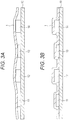
- Figs. 3A and 3B are schematic cross-sectional views for explaining a method of using the electromagnetic wave shielding film.
- a plurality of kinds of electronic components 11 to 14 is mounted on a mounting surface side of a wiring substrate 10 (see FIG. 3A ). Heights of these electronic components 11 to 14 are not uniform. As shown in Fig. 3A , the electromagnetic wave shielding film 1 is mounted on the wiring substrate 10 so that a surface thereof on the adhesion layer 4 side faces the mounting surface of the wiring substrate 10 and the electromagnetic wave shielding film 1 covers the electronic components 11 to 14. Thus, the electromagnetic wave shielding film 1 is fixed to the wiring substrate 10.
- the electromagnetic wave shielding film 1 is lightly pressed against the mounting surface side of the wiring substrate 10 by a jig made of flexible rubber or the like. Then, since the electromagnetic wave shielding film 1 has the conductive layer 3, having the stretchability and having the property of hardly returning to the original state when once stretched, the electromagnetic wave shielding film 1 is stretched as shown in Fig. 3B . Then, the electromagnetic wave shielding film 1 is deformed along outer surfaces (upper surfaces and side surfaces) of the electronic components 11 to 14 on the wiring substrate 10. Then, the electromagnetic wave shielding film 1 maintains this state. Thus, it is possible to reduce a space formed between the electromagnetic wave shielding film 1 and the electronic components 11 to 14 on the wiring substrate 10. As a result, it is possible to increase the electromagnetic wave shielding effect.
- a through-hole 2a extending from a surface of the insulating layer 2 to the conductive layer 3 may be formed, and a pad 5 electrically connected to the conductive layer 3 may be formed on the insulating layer 2.
- the pad 5 can be connected to a ground via a wiring 6.
- a position of the pad 5 may be arbitrary. The position may be an upper portion covered with the electromagnetic wave shielding film 1 on the electronic component. Further, the ground need not be a ground dedicated wiring. Furthermore, the ground may be a housing of an electronic device.
- the electromagnetic wave shielding film 1 includes the insulating layer 2, the conductive layer 3 formed on the one surface of the insulating layer 2 and having stretchability and the property of hardly returning to the original state when once stretched, and the insulating adhesion layer 4 formed on the surface opposite to the insulating layer 2 side of the conductive layer 3.
- the insulating layer 2 may not be formed.
Landscapes
- Engineering & Computer Science (AREA)
- Chemical & Material Sciences (AREA)
- Microelectronics & Electronic Packaging (AREA)
- Physics & Mathematics (AREA)
- Electromagnetism (AREA)
- Life Sciences & Earth Sciences (AREA)
- Materials Engineering (AREA)
- Wood Science & Technology (AREA)
- Organic Chemistry (AREA)
- Inorganic Chemistry (AREA)
- Nanotechnology (AREA)
- Shielding Devices Or Components To Electric Or Magnetic Fields (AREA)
- Laminated Bodies (AREA)
Abstract
Description
- The present invention relates to an electromagnetic wave shielding film.
- An electromagnetic wave shielding material including a pressure sensitive adhesive, a conductive nonwoven fabric layer formed on the pressure sensitive adhesive, and an insulating layer formed on the conductive nonwoven fabric layer has been proposed. The conductive nonwoven fabric is a nonwoven fabric knitted with fibers coated with a metal thin film.
- PATENT LITERATURE 1:
JP-A-2000-036686 - The above-described conventional electromagnetic wave shielding material is provided, for example, on a mounting surface side of a wiring substrate (printed circuit board) so as to cover an electronic component mounted on the printed circuit board. A plurality of electronic components is mounted on the mounting surface of the wiring substrate. Therefore, the surface of the wiring substrate on which the electronic components are mounted has irregularities. The conventional electromagnetic wave shielding material includes a conductive nonwoven fabric layer. Thus, the electromagnetic wave shielding material has almost no stretchability. Therefore, when the electromagnetic wave shielding material is provided on the surface of the wiring substrate on which the electronic components are mounted, a space is easily formed between the electronic components and the electromagnetic wave shielding material. As a result, electromagnetic wave leakage occurs and electromagnetic wave shielding effect is deteriorated.
- An object of the present invention is to provide an electromagnetic wave shielding film capable of reducing a space formed between the electromagnetic wave shielding film and an electronic component on a wiring substrate, and to, therefore, increase an electromagnetic wave shielding effect as a result.
- The invention described in
claim 1 is an electromagnetic wave shielding film including a conductive layer having stretchability, and an adhesion layer formed on one surface of the conductive layer and having insulating properties, wherein the conductive layer includes a conductive composition comprising a resin having stretchability and a conductive filler filled with the resin, and the resin has a tensile permanent set of 2.5% or more and 90% or less. - In this configuration, the electromagnetic wave shielding film includes the conductive layer having stretchability. The conductive layer includes the resin having stretchability and having a tensile permanent set of 2.5% or more and 90% or less. Therefore, the electromagnetic wave shielding film has stretchability and has a property of hardly returning to an original state thereof when once stretched.
- The electromagnetic wave shielding film is applied to, for example, a wiring substrate having an electronic component mounted thereon. In this case, the electromagnetic wave shielding film is mounted on the wiring substrate so that its surface on the adhesive layer side faces the mounting surface of the wiring substrate and it covers the electronic component. Thus, the electromagnetic wave shielding film is temporarily fixed to the wiring substrate. Thereafter, the electromagnetic wave shielding film is lightly pressed against the mounting surface side of the wiring substrate. The electromagnetic wave shielding film has stretchability and has the property of hardly returning to the original state when once stretched. Therefore, the electromagnetic wave shielding film is stretched, to be deformed along an outer surface of the electronic component on the wiring substrate. The electromagnetic wave shielding film maintains this state. Thus, it is possible to reduce the space formed between the electromagnetic wave shielding film and the electronic component on the wiring substrate. Therefore, it is possible to increase the electromagnetic wave shielding effect.
- The invention described in
claim 2 is the electromagnetic wave shielding film according toclaim 1, wherein the resin has a breaking strength of 20MPa or more and 80MPa or less and an elongation at break of 300% or more and 700% or less. - The invention described in
claim 3 is the electromagnetic wave shielding film according toclaim - The invention described in
claim 4 is the electromagnetic wave shielding film according to any one ofclaims 1 to 3, wherein the conductive filler is dendritic. - The invention described in claim 5 is the electromagnetic wave shielding film according to
claim 4, wherein the conductive filler is silver powder. - The invention described in claim 6 is the electromagnetic wave shielding film according to
claim 4, wherein the conductive filler is copper powder. - The invention described in claim 7 is the electromagnetic wave shielding film according to
claim 4, wherein the conductive filler is silver-coated copper powder made of copper powder coated with silver. - The invention described in claim 8 is the electromagnetic wave shielding film according to any one of
claims 1 to 3, wherein the conductive filler has a coil shape. -
-
Fig. 1 is a schematic cross-sectional view showing a configuration of an electromagnetic wave shielding film according to an embodiment of the present invention. -
Fig. 2A is a schematic cross-sectional view showing a process of producing the electromagnetic wave shielding film ofFig. 1. Fig. 2B is a schematic cross-sectional view showing a process followingFig. 2A . -
Figs. 3A and 3B are schematic cross-sectional views for explaining a method of using the electromagnetic wave shielding film ofFig. 1 . -
Fig. 4 is a schematic cross-sectional view showing an example of a method of grounding a conductive layer of the electromagnetic wave shielding film. -
Fig. 1 is a schematic cross-sectional view showing a configuration of an electromagnetic wave shielding film according to an embodiment of the present invention. - An electromagnetic
wave shielding film 1 includes an insulating layer (a protective layer) 2 having electrical insulation properties, aconductive layer 3, and anadhesive layer 4. Theconductive layer 3 is formed on one surface of theinsulating layer 2, has stretchability, and has a property of hardly returning to an original state thereof when once stretched. Theadhesive layer 4 is formed on a surface opposite to the insulatinglayer 2 side of theconductive layer 3 and has insulating properties. The electromagneticwave shielding film 1 is sheet-like. To have stretchability means to have a property of stretching easily. - The
insulating layer 2 has a thickness of about 5 to 50 µm. Theconductive layer 3 has a thickness of about 10 to 100 µm. The pressuresensitive adhesive 4 has a thickness of about 10 to 150 µm. - As the
adhesion layer 4, for example, an adhesive layer, a hot melt adhesion layer, or the like can be used. - Examples of material of adhesive used for the pressure sensitive adhesive as the
adhesion layer 4 include a rubber-based, an acrylic-based, a polyester-based, a silicone-based, and a urethane-based adhesive. - Examples of material of hot melt adhesive used for the hot melt adhesion layer as the
adhesion layer 4 include thermoplastic resins such as polyester-based, polyurethane-based, polyamide-based, olefin-based and ethylene vinyl acetate-based. The hot melt adhesive in the present invention preferably has a melting point of 130°C or less, a durometer hardness of 95A or less, and an elongation at break of 300% or more. The hot melt adhesive of the present invention more preferably has the melting point of 120°C or less, the durometer hardness of 85A or less, and the elongation at break of 500% or more. More specifically, a polyurethane thermoplastic resin such as "SHM 101-PUR" manufactured by Sheedom Co., Ltd. can be used as the hot melt adhesive. - The
conductive layer 3 is made of a conductive composition, including a resin (hereinafter referred to as a "conductive layer resin") having stretchability and having a property of hardly returning to an original state thereof when once stretched and a conductive filler filled with the resin. - A tensile permanent set of the conductive layer resin is preferably 2.5% or more and 90% or less, and more preferably 20% or more and 80% or less. The reason for this is as follows. The electromagnetic
wave shielding film 1 is arranged along an outer surface shape of electronic components and the like. For this purpose, theconductive layer 3 preferably has stretchability and has a property of hardly returning to an original state thereof when once stretched and has a property of slightly returning after once stretched. Here, when the tensile permanent set of the conductive layer resin is less than 2.5%, it is difficult for theconductive layer 3 to exhibit the property of hardly returning to the original state when once stretched. In addition, when the tensile permanent set of the conductive layer resin exceeds 90%, theconductive layer 3 easily exhibit the property of hardly returning to the original state when once stretched, but it is difficult for theconductive layer 3 to exhibit the property of slightly returning after once stretched. - The conductive layer resin preferably has a breaking strength of 20MPa or more and 80MPa or less. The conductive layer resin preferably has an elongation at break of 300% or more and 700% or less. The conductive layer resin preferably has Shore A strength of 20 or more and 50 or less.
- The conductive layer resin includes an elastomer and a thermoplastic resin. Examples of the elastomer used as the conductive layer resin include resins having elasticity such as a styrene-based elastomer, an olefin-based elastomer, a polyester-based elastomer, a polyurethane-based elastomer, a polyamide-based elastomer, a silicone-based elastomer and the like. The polyurethane-based elastomer includes a hard segment and a soft segment. Examples of soft segments include carbonates, esters, and ethers. Preferred physical properties are the breaking strength of 20 to 80MPa, the elongation at break of 300 to 700%, and the permanent tensile strain of 2.5 to 90%. More preferable physical properties are the breaking strength of 30 to 70MPa, the elongation at break of 400 to 600%, and the tensile permanent set of 20 to 80%.
- Specifically, NE - 8880, MAU - 9022, NE - 310, NE - 302 HV, CU - 8448 or the like manufactured by Dainichiseika Color & Chemicals Mfg. Co., Ltd. can be used. As the polyurethane-based elastomer, PANDEX 372E manufactured by DIC Corporation can be used. The elastomer may contain a single resin or a plurality of kinds of resins. From a viewpoint of improving manufacturability (processability), flexibility and the like, the elastomer may contain additives such as a plasticizer, a processing aid, a crosslinking agent, a vulcanization accelerator, a vulcanization aid, an antioxidant, a softener, or a colorant.
- Table 1 shows the physical properties of Comparative Example and Examples of the conductive layer resin.
[Table 1] Physical properties Comparative Example Example 1 Example 2 Example 3 Viscosity (dPa·s/20°C) 240 275 230 150 Breaking strength (MPa) 76 69 54 30 Elongation at break (%) 340 440 460 550 Permanent strain (%) Breaking 2.6 30 71 - The conductive layer resin of Comparative Example includes the urethane elastomer. The conductive layer resin of Examples 1, 2 and 3 include the urethane elastomer.
- The breaking strength [MPa] is a tensile stress just before breaking. Elongation at break [%] is elongation just before breaking. A method of measuring the breaking strength and the elongation at break is based on JIS K 6251: 2010 (Vulcanized rubber and thermoplastic rubber - Determination of tensile properties). The measuring method will be described in detail below. A method of measuring the tensile permanent set [%] is based on JIS K 6273: 2006 (Vulcanized rubber and thermoplastic rubber - Determination of tensile permanent set, elongation rate and creep rate). The measuring method will be described in detail below.
- The method of measuring the breaking strength and the elongation at break will be described. A test piece having a length of 20 mm, a width of 15 mm, and a thickness of 40 ± 5 µm is prepared in advance for each of Comparative Example, Example 1, Example 2 and Example 3. The test piece is attached to a tensile strain retainer. Then, the test piece is pulled until the test piece is broken at a speed of 200 mm/min. A load and an elongation rate just before the test piece breaks are respectively determined as the breaking strength and the elongation at break.
- The method of measuring the tensile permanent set will be described.
- The test piece having a length of 20 mm, a width of 15 mm, and a thickness of 40 ± 5 µm is prepared in advance for each of Comparative Example, Example 1, Example 2 and Example 3.
- The test piece is attached to the tensile strain retainer. Then, the test piece is stretched to a length (60 mm) corresponding to the elongation rate of 200% at the speed of 200 mm/min. The test piece is held for 10 minutes in a state of being stretched to 60 mm. Thereafter, the test piece is detached from the tensile strain retainer. Then, the test piece is allowed to stand for 30 minutes with a pulling force released. When the 30 minutes have elapsed, a length of the test piece (length of the test piece after shrinkage) is measured.
- When the length of the initial test piece is L0, the length of the test piece after elongation is L1, and the length of the test piece after shrinkage is L2, a tensile permanent set TS is expressed by the following equation (1).

- The conductive layer resin of Examples 1, 2, and 3 exhibited a property that it was easy to stretch when pulled and hard to return to the original state when once stretched. In contrast, the conductive layer resin of Comparative Example exhibited a property that it was hard to stretch and easy to break when stretched.
- From such a fact, in order to have stretchability and obtain a property of hardly returning to the original state when once stretched, it can be inferred that the tensile permanent set of the conductive layer resin is preferably 2.5% or more and 90% or less, and more preferably 20% or more and 80% or less. Further, it is inferred that the breaking strength of the conductive layer resin is preferably 20MPa or more and 80MPa or less. Further, it can be inferred that the elongation at break of the conductive layer resin is preferably 300% or more and 700% or less.
- A shape of the conductive filler may be dendrite, coil, bulk, sphere, flake, needle, fiber, or the like. The dendrite shape refers to a shape of a rod-like main branch having a rod-like bifurcated branch extending in two-dimensional direction or three-dimensional direction. Further, the dendrite shape includes a shape having the bifurcated branch bent in the middle and a shape having a rod-like bifurcated branch further extending from the middle of the bifurcated branch.
- The dendritic conductive filler will be described in detail. The dendritic conductive filler may be, for example, dendritic copper powder or silver powder. Or, the conductive filler may be silver-coated copper powder made of dendritic copper powder coated with silver. Further, the conductive filler may be gold-coated copper powder made of dendritic copper powder coated with gold. When the conductive filler is made of dendritic silver-coated copper powder, the conductive filler has a resistance value close to that of the conductive filler made of silver although it is relatively inexpensive. That is, the conductive filler having excellent conductivity and migration resistance can be realized. Further, when the conductive filler is made of dendritic copper powder, it is possible to realize the conductive filler having a low resistance value although it is inexpensive.
- When the conductive filler is made of dendritic silver-coated copper powder, the polyurethane-based elastomer is preferably used as the elastomer. In this case, the polyurethane-based elastomer has a volume resistivity of 1010-13 Qcm lower by about two digits than other elastomers. Further, the polyurethane-based elastomer has a high affinity to the conductive filler containing silver. Therefore, it is possible to stretch the conductive composition satisfactorily.
- A lower limit of an average particle size of the conductive filler is 1 µm, preferably 2 µm. When the lower limit is 1 µm or more, the conductive fillers tend to come into contact with each other. Therefore, the conductive composition has excellent conductivity. An upper limit of the average particle size of the conductive filler is 20 µm, preferably 10 µm. When the upper limit is 20 µm or less, the thickness of the conductive layer made of conductive composition can be reduced.
- With the conductive filler having a coil shape (including a helix shape and a spiral shape), when the elastomer is stretched, the conductive filler is stretched as when the coil is pulled. Therefore, even when the elastomer is stretched, it is possible to suppress the conductive composition from increasing in the resistance value. Thus, it is possible to provide the conductive composition having stretchability and capable of suppressing an increase in the resistance value when stretched.
- A filling rate of the conductive filler in the conductive composition (conductive layer 3) is preferably 60 mass% or more and 90 mass% or less.
- A conductive paste used for forming the
conductive layer 3 can be produced, for example, as follows. For example, the dendritic silver-coated copper powder having an average particle size of 5 µm was blended to the conductive layer resin so that the filling rate of the silver-coated copper powder (filling rate of the conductive filler in the conductive composition) is a predetermined mass% (for example, 80 mass%). Next, for example, 40 parts by mass of a mixed solvent of isopropyl alcohol and toluene (a weight ratio of isopropyl alcohol to toluene is, for example, 5:5) is added to 100 parts by mass of the conductive layer resin. Next, stirring by a planetary stirrer was performed. Thus, a solution (the conductive paste) containing the conductive layer resin, the silver-coated copper powder and an organic solvent was obtained. It goes without saying that dendritic conductive fillers such as dendritic silver powder, or coil-shaped conductive fillers or the like can be used instead of the dendritic silver-coated copper powder. - As the insulating
layer 2, for example, the elastomer used as the above-described conductive layer resin filled with carbon black can be used. Similarly, the insulatinglayer 2 may contain the additives such as the plasticizer, the processing aid, the crosslinking agent, the vulcanization accelerator, the vulcanization aid, the antioxidant, the softener, or the colorant. -
Figs. 2A and 2B are process diagrams showing a method for producing the electromagneticwave shielding film 1. - First, as shown in
Fig. 2A , theconductive layer 3 is formed on the one surface of the insulatinglayer 2. Specifically, the conductive paste which is a material of theconductive layer 3 is applied to the one surface of the insulatinglayer 2. Next, heat drying is performed. Subsequently, as shown inFig. 2B , theadhesion layer 4 is formed on the surface opposite to the insulatinglayer 2 of theconductive layer 3. Thus, the electromagneticwave shielding film 1 is obtained. -
Figs. 3A and 3B are schematic cross-sectional views for explaining a method of using the electromagnetic wave shielding film. - A plurality of kinds of
electronic components 11 to 14 is mounted on a mounting surface side of a wiring substrate 10 (seeFIG. 3A ). Heights of theseelectronic components 11 to 14 are not uniform. As shown inFig. 3A , the electromagneticwave shielding film 1 is mounted on thewiring substrate 10 so that a surface thereof on theadhesion layer 4 side faces the mounting surface of thewiring substrate 10 and the electromagneticwave shielding film 1 covers theelectronic components 11 to 14. Thus, the electromagneticwave shielding film 1 is fixed to thewiring substrate 10. - Thereafter, the electromagnetic
wave shielding film 1 is lightly pressed against the mounting surface side of thewiring substrate 10 by a jig made of flexible rubber or the like. Then, since the electromagneticwave shielding film 1 has theconductive layer 3, having the stretchability and having the property of hardly returning to the original state when once stretched, the electromagneticwave shielding film 1 is stretched as shown inFig. 3B . Then, the electromagneticwave shielding film 1 is deformed along outer surfaces (upper surfaces and side surfaces) of theelectronic components 11 to 14 on thewiring substrate 10. Then, the electromagneticwave shielding film 1 maintains this state. Thus, it is possible to reduce a space formed between the electromagneticwave shielding film 1 and theelectronic components 11 to 14 on thewiring substrate 10. As a result, it is possible to increase the electromagnetic wave shielding effect. - As shown in
Fig. 4 , a through-hole 2a extending from a surface of the insulatinglayer 2 to theconductive layer 3 may be formed, and a pad 5 electrically connected to theconductive layer 3 may be formed on the insulatinglayer 2. The pad 5 can be connected to a ground via a wiring 6. A position of the pad 5 may be arbitrary. The position may be an upper portion covered with the electromagneticwave shielding film 1 on the electronic component. Further, the ground need not be a ground dedicated wiring. Furthermore, the ground may be a housing of an electronic device. - In the above-described embodiment, the electromagnetic
wave shielding film 1 includes the insulatinglayer 2, theconductive layer 3 formed on the one surface of the insulatinglayer 2 and having stretchability and the property of hardly returning to the original state when once stretched, and the insulatingadhesion layer 4 formed on the surface opposite to the insulatinglayer 2 side of theconductive layer 3. However, the insulatinglayer 2 may not be formed. - In addition, it is possible to make various design changes within the scope of matters described in claims.
- The present international application is a priority claimed application based on Japanese Patent Application No.
2016-072293 filed on Mar. 31, 2016 2016-072293 - The above descriptions of a specific embodiment of the present invention have been presented for the purpose of exemplification. They are not intended to be exhaustive or to limit the present invention to the described embodiment. It will be apparent to those skilled in the art that numerous variations or modifications can be made in light of the above description.
-
- 1:
- Electromagnetic wave shielding film
- 2:
- Insulating layer
- 3:
- Conductive layer
- 4:
- Adhesion layer
Claims (8)
- An electromagnetic wave shielding film comprising:a conductive layer having stretchability; andan adhesion layer formed on one surface of the conductive layer and having insulating properties, whereinthe conductive layer includes a conductive composition comprising a resin having stretchability and a conductive filler filled with the resin, andthe resin has a tensile permanent set of 2.5% or more and 90% or less.
- The electromagnetic wave shielding film according to claim 1, wherein
the resin has a breaking strength of 20MPa or more and 80MPa or less and an elongation at break of 300% or more and 700% or less. - The electromagnetic wave shielding film according to claim 1 or 2, further comprising an insulating layer formed on a surface opposite to the adhesion layer side of the conductive layer.
- The electromagnetic wave shielding film according to any one of claims 1 to 3, wherein
the conductive filler is dendritic. - The electromagnetic wave shielding film according to claim 4, wherein
the conductive filler is silver powder. - The electromagnetic wave shielding film according to claim 4, wherein
the conductive filler is copper powder. - The electromagnetic wave shielding film according to claim 4, wherein
the conductive filler is silver-coated copper powder made of copper powder coated with silver. - The electromagnetic wave shielding film according to any one of claims 1 to 3, wherein
the conductive filler has a coil shape.
Applications Claiming Priority (2)
| Application Number | Priority Date | Filing Date | Title |
|---|---|---|---|
| JP2016072293A JP6757163B2 (en) | 2016-03-31 | 2016-03-31 | Electromagnetic wave shield film |
| PCT/JP2017/006301 WO2017169297A1 (en) | 2016-03-31 | 2017-02-21 | Electromagnetic-wave shield film |
Publications (2)
| Publication Number | Publication Date |
|---|---|
| EP3439447A1 true EP3439447A1 (en) | 2019-02-06 |
| EP3439447A4 EP3439447A4 (en) | 2019-11-27 |
Family
ID=59963054
Family Applications (1)
| Application Number | Title | Priority Date | Filing Date |
|---|---|---|---|
| EP17773845.7A Pending EP3439447A4 (en) | 2016-03-31 | 2017-02-21 | SHIELDING FILM AGAINST ELECTROMAGNETIC WAVES |
Country Status (7)
| Country | Link |
|---|---|
| US (1) | US11812543B2 (en) |
| EP (1) | EP3439447A4 (en) |
| JP (1) | JP6757163B2 (en) |
| KR (1) | KR102564763B1 (en) |
| CN (1) | CN108886884B (en) |
| TW (1) | TWI707629B (en) |
| WO (1) | WO2017169297A1 (en) |
Families Citing this family (6)
| Publication number | Priority date | Publication date | Assignee | Title |
|---|---|---|---|---|
| KR102537591B1 (en) | 2018-04-25 | 2023-06-02 | 삼성디스플레이 주식회사 | Method and apparatus for manufacturing a display device |
| KR102820004B1 (en) | 2019-06-17 | 2025-06-13 | 삼성디스플레이 주식회사 | Display device and method for manufacturimg display device |
| KR102047831B1 (en) | 2019-07-09 | 2019-11-22 | 한국생산기술연구원 | Liquid metal particle coating sheet member having electromagnetic wave shielding function and heat dissipation function and method of preparing the same |
| KR20210007103A (en) | 2019-07-10 | 2021-01-20 | 한국생산기술연구원 | Film member including liquid metal particle |
| CN112654129B (en) * | 2019-10-10 | 2021-11-16 | 庆鼎精密电子(淮安)有限公司 | Anti-electromagnetic interference circuit board and manufacturing method thereof |
| CN120417357B (en) * | 2025-05-14 | 2025-12-02 | 北京魁冠科技有限公司 | An electromagnetic shielding cover and circuit board |
Family Cites Families (17)
| Publication number | Priority date | Publication date | Assignee | Title |
|---|---|---|---|---|
| JP2000036686A (en) | 1998-07-16 | 2000-02-02 | Kiyohiro Takahashi | Electromagnetic shield member |
| US7323214B2 (en) | 2001-11-09 | 2008-01-29 | Tdk Corporation | Composite magnetic material electromagnetic wave absorbing sheet method for manufacturing sheet-like product and method for manufacturing electromagnetic wave absorbing sheet |
| JP2005532417A (en) | 2001-12-19 | 2005-10-27 | イー・アイ・デュポン・ドウ・ヌムール・アンド・カンパニー | Polyamide resin composition having electromagnetic wave shielding characteristics and article formed therefrom |
| JP2004176005A (en) | 2002-11-29 | 2004-06-24 | Kinugawa Rubber Ind Co Ltd | Conductive elastomer composition and production method thereof |
| JP2007027522A (en) * | 2005-07-20 | 2007-02-01 | Toyo Kohan Co Ltd | Electromagnetic shield material and electromagnetic shield member |
| WO2007083822A1 (en) | 2006-01-17 | 2007-07-26 | Seiren Co., Ltd. | Electroconductive gasket material |
| JP4947275B2 (en) | 2006-07-18 | 2012-06-06 | 株式会社スリーボンド | Electronic component protective sheet and coating method |
| CN101050307B (en) | 2007-04-24 | 2010-12-15 | 上海材料研究所 | A kind of conductive silicone rubber with electromagnetic shielding performance and its manufacturing method |
| US8048690B2 (en) * | 2007-11-08 | 2011-11-01 | Nitto Denko Corporation | Pressure-sensitive adhesive sheet and process for producing semiconductor device having same |
| JP2009138141A (en) | 2007-12-07 | 2009-06-25 | Hitachi Cable Ltd | Method for producing conductive rubber and conductive rubber |
| JP2014078573A (en) * | 2012-10-10 | 2014-05-01 | Toyo Ink Sc Holdings Co Ltd | Electromagnetic wave-shielding coverlay film, method for manufacturing flexible printed wiring board, and flexible printed wiring board |
| CN103763893B (en) | 2014-01-14 | 2016-04-13 | 广州方邦电子股份有限公司 | Electromagnetic shielding film and comprise the manufacture method of wiring board of screened film |
| JP6650660B2 (en) * | 2014-01-20 | 2020-02-19 | 東洋インキScホールディングス株式会社 | Electromagnetic wave shielding sheet for flexible printed wiring board and flexible printed wiring board with electromagnetic wave shielding sheet |
| WO2016017644A1 (en) * | 2014-07-31 | 2016-02-04 | タツタ電線株式会社 | Conductive composition and conductive sheet provided with same |
| JP5861790B1 (en) * | 2015-02-25 | 2016-02-16 | 東洋インキScホールディングス株式会社 | Electromagnetic shielding sheet, electromagnetic shielding wiring circuit board, and electronic equipment |
| CN105237890A (en) * | 2015-11-02 | 2016-01-13 | 深圳德邦界面材料有限公司 | EPDM/PP thermoplastic elastomer with electromagnetic shielding property |
| JP6660542B2 (en) * | 2015-11-30 | 2020-03-11 | タツタ電線株式会社 | Stretchable conductive film for textile |
-
2016
- 2016-03-31 JP JP2016072293A patent/JP6757163B2/en active Active
- 2016-12-05 TW TW105140099A patent/TWI707629B/en active
-
2017
- 2017-02-21 EP EP17773845.7A patent/EP3439447A4/en active Pending
- 2017-02-21 CN CN201780019482.7A patent/CN108886884B/en active Active
- 2017-02-21 US US16/087,698 patent/US11812543B2/en active Active
- 2017-02-21 KR KR1020187028540A patent/KR102564763B1/en active Active
- 2017-02-21 WO PCT/JP2017/006301 patent/WO2017169297A1/en not_active Ceased
Also Published As
| Publication number | Publication date |
|---|---|
| US20190098742A1 (en) | 2019-03-28 |
| CN108886884B (en) | 2020-10-13 |
| KR20180127386A (en) | 2018-11-28 |
| JP2017183644A (en) | 2017-10-05 |
| CN108886884A (en) | 2018-11-23 |
| TWI707629B (en) | 2020-10-11 |
| US11812543B2 (en) | 2023-11-07 |
| KR102564763B1 (en) | 2023-08-07 |
| EP3439447A4 (en) | 2019-11-27 |
| WO2017169297A1 (en) | 2017-10-05 |
| TW201811158A (en) | 2018-03-16 |
| JP6757163B2 (en) | 2020-09-16 |
Similar Documents
| Publication | Publication Date | Title |
|---|---|---|
| US11812543B2 (en) | Electromagnetic wave shielding film | |
| EP3273754B1 (en) | Stretchable cable and stretchable circuit board | |
| CN108701505B (en) | Stretchable conductor sheet, adhesive stretchable conductor sheet, and method of forming wiring composed of stretchable conductor on fabric | |
| US20200146143A1 (en) | Elastic Wiring Member | |
| KR0149738B1 (en) | Sealed Flat Cable | |
| EP3196257A1 (en) | Conductive composition and conductive sheet provided with same | |
| KR20180088832A (en) | Stretchable conductive film for textile | |
| KR101993813B1 (en) | Room temperature liquid metal capsule ink, method of manufacturing the same, and room temperature liquid metal capsule conductive wire formed by the same | |
| KR20190033567A (en) | Stretchable electrically conductive adhesive tape | |
| CN113545173A (en) | Stretchable circuit board | |
| WO2020203037A1 (en) | Electrical connection member and terminal-attached glass plate structure | |
| KR100762854B1 (en) | Ground Foam Gasket for Surface Mounting of Electronic Circuit Board and Manufacturing Method | |
| JP6639079B2 (en) | Anisotropic conductive material | |
| CN113261393A (en) | Lead, electronic equipment and manufacturing method of lead | |
| JP7414208B2 (en) | Telescopic wiring member | |
| JPH11330777A (en) | Sealing member composition excellent in electromagnetic shielding property and sealing member | |
| CN218274079U (en) | Bending-resistant waterproof radio frequency cable | |
| Hosono et al. | Variation in electrical resistivity of stretchable printed wires composed a polyurethane-based binder containing silver fillers under cyclic tensions | |
| KR100739470B1 (en) | Manufacturing method of static protection shoe |
Legal Events
| Date | Code | Title | Description |
|---|---|---|---|
| STAA | Information on the status of an ep patent application or granted ep patent |
Free format text: STATUS: THE INTERNATIONAL PUBLICATION HAS BEEN MADE |
|
| PUAI | Public reference made under article 153(3) epc to a published international application that has entered the european phase |
Free format text: ORIGINAL CODE: 0009012 |
|
| STAA | Information on the status of an ep patent application or granted ep patent |
Free format text: STATUS: REQUEST FOR EXAMINATION WAS MADE |
|
| 17P | Request for examination filed |
Effective date: 20181026 |
|
| AK | Designated contracting states |
Kind code of ref document: A1 Designated state(s): AL AT BE BG CH CY CZ DE DK EE ES FI FR GB GR HR HU IE IS IT LI LT LU LV MC MK MT NL NO PL PT RO RS SE SI SK SM TR |
|
| AX | Request for extension of the european patent |
Extension state: BA ME |
|
| DAV | Request for validation of the european patent (deleted) | ||
| DAX | Request for extension of the european patent (deleted) | ||
| A4 | Supplementary search report drawn up and despatched |
Effective date: 20191028 |
|
| RIC1 | Information provided on ipc code assigned before grant |
Ipc: B32B 27/18 20060101ALI20191022BHEP Ipc: H05K 9/00 20060101AFI20191022BHEP Ipc: B32B 7/02 20190101ALI20191022BHEP |
|
| STAA | Information on the status of an ep patent application or granted ep patent |
Free format text: STATUS: EXAMINATION IS IN PROGRESS |
|
| 17Q | First examination report despatched |
Effective date: 20210813 |