EP3439036A1 - Thin film transistor and display device including thin film transistor - Google Patents
Thin film transistor and display device including thin film transistor Download PDFInfo
- Publication number
- EP3439036A1 EP3439036A1 EP18182271.9A EP18182271A EP3439036A1 EP 3439036 A1 EP3439036 A1 EP 3439036A1 EP 18182271 A EP18182271 A EP 18182271A EP 3439036 A1 EP3439036 A1 EP 3439036A1
- Authority
- EP
- European Patent Office
- Prior art keywords
- semiconductor layer
- type semiconductor
- contact hole
- gate electrode
- thin film
- Prior art date
- Legal status (The legal status is an assumption and is not a legal conclusion. Google has not performed a legal analysis and makes no representation as to the accuracy of the status listed.)
- Granted
Links
Images





Classifications
-
- H—ELECTRICITY
- H10—SEMICONDUCTOR DEVICES; ELECTRIC SOLID-STATE DEVICES NOT OTHERWISE PROVIDED FOR
- H10D—INORGANIC ELECTRIC SEMICONDUCTOR DEVICES
- H10D30/00—Field-effect transistors [FET]
- H10D30/60—Insulated-gate field-effect transistors [IGFET]
- H10D30/67—Thin-film transistors [TFT]
-
- G—PHYSICS
- G02—OPTICS
- G02F—OPTICAL DEVICES OR ARRANGEMENTS FOR THE CONTROL OF LIGHT BY MODIFICATION OF THE OPTICAL PROPERTIES OF THE MEDIA OF THE ELEMENTS INVOLVED THEREIN; NON-LINEAR OPTICS; FREQUENCY-CHANGING OF LIGHT; OPTICAL LOGIC ELEMENTS; OPTICAL ANALOGUE/DIGITAL CONVERTERS
- G02F1/00—Devices or arrangements for the control of the intensity, colour, phase, polarisation or direction of light arriving from an independent light source, e.g. switching, gating or modulating; Non-linear optics
- G02F1/01—Devices or arrangements for the control of the intensity, colour, phase, polarisation or direction of light arriving from an independent light source, e.g. switching, gating or modulating; Non-linear optics for the control of the intensity, phase, polarisation or colour
- G02F1/13—Devices or arrangements for the control of the intensity, colour, phase, polarisation or direction of light arriving from an independent light source, e.g. switching, gating or modulating; Non-linear optics for the control of the intensity, phase, polarisation or colour based on liquid crystals, e.g. single liquid crystal display cells
- G02F1/133—Constructional arrangements; Operation of liquid crystal cells; Circuit arrangements
- G02F1/136—Liquid crystal cells structurally associated with a semi-conducting layer or substrate, e.g. cells forming part of an integrated circuit
- G02F1/1362—Active matrix addressed cells
- G02F1/1368—Active matrix addressed cells in which the switching element is a three-electrode device
-
- G—PHYSICS
- G09—EDUCATION; CRYPTOGRAPHY; DISPLAY; ADVERTISING; SEALS
- G09G—ARRANGEMENTS OR CIRCUITS FOR CONTROL OF INDICATING DEVICES USING STATIC MEANS TO PRESENT VARIABLE INFORMATION
- G09G3/00—Control arrangements or circuits, of interest only in connection with visual indicators other than cathode-ray tubes
- G09G3/20—Control arrangements or circuits, of interest only in connection with visual indicators other than cathode-ray tubes for presentation of an assembly of a number of characters, e.g. a page, by composing the assembly by combination of individual elements arranged in a matrix no fixed position being assigned to or needed to be assigned to the individual characters or partial characters
-
- G—PHYSICS
- G09—EDUCATION; CRYPTOGRAPHY; DISPLAY; ADVERTISING; SEALS
- G09G—ARRANGEMENTS OR CIRCUITS FOR CONTROL OF INDICATING DEVICES USING STATIC MEANS TO PRESENT VARIABLE INFORMATION
- G09G3/00—Control arrangements or circuits, of interest only in connection with visual indicators other than cathode-ray tubes
- G09G3/20—Control arrangements or circuits, of interest only in connection with visual indicators other than cathode-ray tubes for presentation of an assembly of a number of characters, e.g. a page, by composing the assembly by combination of individual elements arranged in a matrix no fixed position being assigned to or needed to be assigned to the individual characters or partial characters
- G09G3/22—Control arrangements or circuits, of interest only in connection with visual indicators other than cathode-ray tubes for presentation of an assembly of a number of characters, e.g. a page, by composing the assembly by combination of individual elements arranged in a matrix no fixed position being assigned to or needed to be assigned to the individual characters or partial characters using controlled light sources
- G09G3/30—Control arrangements or circuits, of interest only in connection with visual indicators other than cathode-ray tubes for presentation of an assembly of a number of characters, e.g. a page, by composing the assembly by combination of individual elements arranged in a matrix no fixed position being assigned to or needed to be assigned to the individual characters or partial characters using controlled light sources using electroluminescent panels
- G09G3/32—Control arrangements or circuits, of interest only in connection with visual indicators other than cathode-ray tubes for presentation of an assembly of a number of characters, e.g. a page, by composing the assembly by combination of individual elements arranged in a matrix no fixed position being assigned to or needed to be assigned to the individual characters or partial characters using controlled light sources using electroluminescent panels semiconductive, e.g. using light-emitting diodes [LED]
- G09G3/3208—Control arrangements or circuits, of interest only in connection with visual indicators other than cathode-ray tubes for presentation of an assembly of a number of characters, e.g. a page, by composing the assembly by combination of individual elements arranged in a matrix no fixed position being assigned to or needed to be assigned to the individual characters or partial characters using controlled light sources using electroluminescent panels semiconductive, e.g. using light-emitting diodes [LED] organic, e.g. using organic light-emitting diodes [OLED]
- G09G3/3225—Control arrangements or circuits, of interest only in connection with visual indicators other than cathode-ray tubes for presentation of an assembly of a number of characters, e.g. a page, by composing the assembly by combination of individual elements arranged in a matrix no fixed position being assigned to or needed to be assigned to the individual characters or partial characters using controlled light sources using electroluminescent panels semiconductive, e.g. using light-emitting diodes [LED] organic, e.g. using organic light-emitting diodes [OLED] using an active matrix
-
- G—PHYSICS
- G09—EDUCATION; CRYPTOGRAPHY; DISPLAY; ADVERTISING; SEALS
- G09G—ARRANGEMENTS OR CIRCUITS FOR CONTROL OF INDICATING DEVICES USING STATIC MEANS TO PRESENT VARIABLE INFORMATION
- G09G3/00—Control arrangements or circuits, of interest only in connection with visual indicators other than cathode-ray tubes
- G09G3/20—Control arrangements or circuits, of interest only in connection with visual indicators other than cathode-ray tubes for presentation of an assembly of a number of characters, e.g. a page, by composing the assembly by combination of individual elements arranged in a matrix no fixed position being assigned to or needed to be assigned to the individual characters or partial characters
- G09G3/22—Control arrangements or circuits, of interest only in connection with visual indicators other than cathode-ray tubes for presentation of an assembly of a number of characters, e.g. a page, by composing the assembly by combination of individual elements arranged in a matrix no fixed position being assigned to or needed to be assigned to the individual characters or partial characters using controlled light sources
- G09G3/30—Control arrangements or circuits, of interest only in connection with visual indicators other than cathode-ray tubes for presentation of an assembly of a number of characters, e.g. a page, by composing the assembly by combination of individual elements arranged in a matrix no fixed position being assigned to or needed to be assigned to the individual characters or partial characters using controlled light sources using electroluminescent panels
- G09G3/32—Control arrangements or circuits, of interest only in connection with visual indicators other than cathode-ray tubes for presentation of an assembly of a number of characters, e.g. a page, by composing the assembly by combination of individual elements arranged in a matrix no fixed position being assigned to or needed to be assigned to the individual characters or partial characters using controlled light sources using electroluminescent panels semiconductive, e.g. using light-emitting diodes [LED]
- G09G3/3208—Control arrangements or circuits, of interest only in connection with visual indicators other than cathode-ray tubes for presentation of an assembly of a number of characters, e.g. a page, by composing the assembly by combination of individual elements arranged in a matrix no fixed position being assigned to or needed to be assigned to the individual characters or partial characters using controlled light sources using electroluminescent panels semiconductive, e.g. using light-emitting diodes [LED] organic, e.g. using organic light-emitting diodes [OLED]
- G09G3/3275—Details of drivers for data electrodes
- G09G3/3291—Details of drivers for data electrodes in which the data driver supplies a variable data voltage for setting the current through, or the voltage across, the light-emitting elements
-
- G—PHYSICS
- G09—EDUCATION; CRYPTOGRAPHY; DISPLAY; ADVERTISING; SEALS
- G09G—ARRANGEMENTS OR CIRCUITS FOR CONTROL OF INDICATING DEVICES USING STATIC MEANS TO PRESENT VARIABLE INFORMATION
- G09G3/00—Control arrangements or circuits, of interest only in connection with visual indicators other than cathode-ray tubes
- G09G3/20—Control arrangements or circuits, of interest only in connection with visual indicators other than cathode-ray tubes for presentation of an assembly of a number of characters, e.g. a page, by composing the assembly by combination of individual elements arranged in a matrix no fixed position being assigned to or needed to be assigned to the individual characters or partial characters
- G09G3/34—Control arrangements or circuits, of interest only in connection with visual indicators other than cathode-ray tubes for presentation of an assembly of a number of characters, e.g. a page, by composing the assembly by combination of individual elements arranged in a matrix no fixed position being assigned to or needed to be assigned to the individual characters or partial characters by control of light from an independent source
- G09G3/36—Control arrangements or circuits, of interest only in connection with visual indicators other than cathode-ray tubes for presentation of an assembly of a number of characters, e.g. a page, by composing the assembly by combination of individual elements arranged in a matrix no fixed position being assigned to or needed to be assigned to the individual characters or partial characters by control of light from an independent source using liquid crystals
- G09G3/3611—Control of matrices with row and column drivers
- G09G3/3648—Control of matrices with row and column drivers using an active matrix
-
- H—ELECTRICITY
- H10—SEMICONDUCTOR DEVICES; ELECTRIC SOLID-STATE DEVICES NOT OTHERWISE PROVIDED FOR
- H10D—INORGANIC ELECTRIC SEMICONDUCTOR DEVICES
- H10D30/00—Field-effect transistors [FET]
- H10D30/60—Insulated-gate field-effect transistors [IGFET]
- H10D30/67—Thin-film transistors [TFT]
- H10D30/6729—Thin-film transistors [TFT] characterised by the electrodes
-
- H—ELECTRICITY
- H10—SEMICONDUCTOR DEVICES; ELECTRIC SOLID-STATE DEVICES NOT OTHERWISE PROVIDED FOR
- H10D—INORGANIC ELECTRIC SEMICONDUCTOR DEVICES
- H10D30/00—Field-effect transistors [FET]
- H10D30/60—Insulated-gate field-effect transistors [IGFET]
- H10D30/67—Thin-film transistors [TFT]
- H10D30/6729—Thin-film transistors [TFT] characterised by the electrodes
- H10D30/673—Thin-film transistors [TFT] characterised by the electrodes characterised by the shapes, relative sizes or dispositions of the gate electrodes
-
- H—ELECTRICITY
- H10—SEMICONDUCTOR DEVICES; ELECTRIC SOLID-STATE DEVICES NOT OTHERWISE PROVIDED FOR
- H10D—INORGANIC ELECTRIC SEMICONDUCTOR DEVICES
- H10D30/00—Field-effect transistors [FET]
- H10D30/60—Insulated-gate field-effect transistors [IGFET]
- H10D30/67—Thin-film transistors [TFT]
- H10D30/6729—Thin-film transistors [TFT] characterised by the electrodes
- H10D30/673—Thin-film transistors [TFT] characterised by the electrodes characterised by the shapes, relative sizes or dispositions of the gate electrodes
- H10D30/6733—Multi-gate TFTs
- H10D30/6734—Multi-gate TFTs having gate electrodes arranged on both top and bottom sides of the channel, e.g. dual-gate TFTs
-
- H—ELECTRICITY
- H10—SEMICONDUCTOR DEVICES; ELECTRIC SOLID-STATE DEVICES NOT OTHERWISE PROVIDED FOR
- H10D—INORGANIC ELECTRIC SEMICONDUCTOR DEVICES
- H10D30/00—Field-effect transistors [FET]
- H10D30/60—Insulated-gate field-effect transistors [IGFET]
- H10D30/67—Thin-film transistors [TFT]
- H10D30/674—Thin-film transistors [TFT] characterised by the active materials
- H10D30/6755—Oxide semiconductors, e.g. zinc oxide, copper aluminium oxide or cadmium stannate
-
- H—ELECTRICITY
- H10—SEMICONDUCTOR DEVICES; ELECTRIC SOLID-STATE DEVICES NOT OTHERWISE PROVIDED FOR
- H10D—INORGANIC ELECTRIC SEMICONDUCTOR DEVICES
- H10D62/00—Semiconductor bodies, or regions thereof, of devices having potential barriers
- H10D62/10—Shapes, relative sizes or dispositions of the regions of the semiconductor bodies; Shapes of the semiconductor bodies
- H10D62/124—Shapes, relative sizes or dispositions of the regions of semiconductor bodies or of junctions between the regions
-
- H—ELECTRICITY
- H10—SEMICONDUCTOR DEVICES; ELECTRIC SOLID-STATE DEVICES NOT OTHERWISE PROVIDED FOR
- H10D—INORGANIC ELECTRIC SEMICONDUCTOR DEVICES
- H10D86/00—Integrated devices formed in or on insulating or conducting substrates, e.g. formed in silicon-on-insulator [SOI] substrates or on stainless steel or glass substrates
- H10D86/40—Integrated devices formed in or on insulating or conducting substrates, e.g. formed in silicon-on-insulator [SOI] substrates or on stainless steel or glass substrates characterised by multiple TFTs
- H10D86/421—Integrated devices formed in or on insulating or conducting substrates, e.g. formed in silicon-on-insulator [SOI] substrates or on stainless steel or glass substrates characterised by multiple TFTs having a particular composition, shape or crystalline structure of the active layer
- H10D86/423—Integrated devices formed in or on insulating or conducting substrates, e.g. formed in silicon-on-insulator [SOI] substrates or on stainless steel or glass substrates characterised by multiple TFTs having a particular composition, shape or crystalline structure of the active layer comprising semiconductor materials not belonging to the Group IV, e.g. InGaZnO
-
- H—ELECTRICITY
- H10—SEMICONDUCTOR DEVICES; ELECTRIC SOLID-STATE DEVICES NOT OTHERWISE PROVIDED FOR
- H10D—INORGANIC ELECTRIC SEMICONDUCTOR DEVICES
- H10D86/00—Integrated devices formed in or on insulating or conducting substrates, e.g. formed in silicon-on-insulator [SOI] substrates or on stainless steel or glass substrates
- H10D86/40—Integrated devices formed in or on insulating or conducting substrates, e.g. formed in silicon-on-insulator [SOI] substrates or on stainless steel or glass substrates characterised by multiple TFTs
- H10D86/441—Interconnections, e.g. scanning lines
-
- H—ELECTRICITY
- H10—SEMICONDUCTOR DEVICES; ELECTRIC SOLID-STATE DEVICES NOT OTHERWISE PROVIDED FOR
- H10D—INORGANIC ELECTRIC SEMICONDUCTOR DEVICES
- H10D86/00—Integrated devices formed in or on insulating or conducting substrates, e.g. formed in silicon-on-insulator [SOI] substrates or on stainless steel or glass substrates
- H10D86/40—Integrated devices formed in or on insulating or conducting substrates, e.g. formed in silicon-on-insulator [SOI] substrates or on stainless steel or glass substrates characterised by multiple TFTs
- H10D86/471—Integrated devices formed in or on insulating or conducting substrates, e.g. formed in silicon-on-insulator [SOI] substrates or on stainless steel or glass substrates characterised by multiple TFTs having different architectures, e.g. having both top-gate and bottom-gate TFTs
-
- H—ELECTRICITY
- H10—SEMICONDUCTOR DEVICES; ELECTRIC SOLID-STATE DEVICES NOT OTHERWISE PROVIDED FOR
- H10D—INORGANIC ELECTRIC SEMICONDUCTOR DEVICES
- H10D86/00—Integrated devices formed in or on insulating or conducting substrates, e.g. formed in silicon-on-insulator [SOI] substrates or on stainless steel or glass substrates
- H10D86/40—Integrated devices formed in or on insulating or conducting substrates, e.g. formed in silicon-on-insulator [SOI] substrates or on stainless steel or glass substrates characterised by multiple TFTs
- H10D86/60—Integrated devices formed in or on insulating or conducting substrates, e.g. formed in silicon-on-insulator [SOI] substrates or on stainless steel or glass substrates characterised by multiple TFTs wherein the TFTs are in active matrices
-
- H—ELECTRICITY
- H10—SEMICONDUCTOR DEVICES; ELECTRIC SOLID-STATE DEVICES NOT OTHERWISE PROVIDED FOR
- H10K—ORGANIC ELECTRIC SOLID-STATE DEVICES
- H10K59/00—Integrated devices, or assemblies of multiple devices, comprising at least one organic light-emitting element covered by group H10K50/00
- H10K59/10—OLED displays
- H10K59/12—Active-matrix OLED [AMOLED] displays
- H10K59/121—Active-matrix OLED [AMOLED] displays characterised by the geometry or disposition of pixel elements
- H10K59/1213—Active-matrix OLED [AMOLED] displays characterised by the geometry or disposition of pixel elements the pixel elements being TFTs
-
- H—ELECTRICITY
- H10—SEMICONDUCTOR DEVICES; ELECTRIC SOLID-STATE DEVICES NOT OTHERWISE PROVIDED FOR
- H10K—ORGANIC ELECTRIC SOLID-STATE DEVICES
- H10K59/00—Integrated devices, or assemblies of multiple devices, comprising at least one organic light-emitting element covered by group H10K50/00
- H10K59/10—OLED displays
- H10K59/12—Active-matrix OLED [AMOLED] displays
- H10K59/131—Interconnections, e.g. wiring lines or terminals
-
- G—PHYSICS
- G09—EDUCATION; CRYPTOGRAPHY; DISPLAY; ADVERTISING; SEALS
- G09G—ARRANGEMENTS OR CIRCUITS FOR CONTROL OF INDICATING DEVICES USING STATIC MEANS TO PRESENT VARIABLE INFORMATION
- G09G2310/00—Command of the display device
- G09G2310/08—Details of timing specific for flat panels, other than clock recovery
-
- H—ELECTRICITY
- H10—SEMICONDUCTOR DEVICES; ELECTRIC SOLID-STATE DEVICES NOT OTHERWISE PROVIDED FOR
- H10D—INORGANIC ELECTRIC SEMICONDUCTOR DEVICES
- H10D30/00—Field-effect transistors [FET]
- H10D30/60—Insulated-gate field-effect transistors [IGFET]
- H10D30/67—Thin-film transistors [TFT]
- H10D30/6757—Thin-film transistors [TFT] characterised by the structure of the channel, e.g. transverse or longitudinal shape or doping profile
Definitions
- the present disclosure relates to a thin film transistor (TFT) and a display device including the TFT.
- TFT thin film transistor
- LCD liquid crystal display
- PDP plasma display panel
- organic light emitting display devices are being practically used.
- Flat panel display devices such as LCD devices and organic light emitting display devices, each include a display panel, a gate driving circuit, a data driving circuit, and a timing controller.
- the display panel includes a plurality of data lines, a plurality of gate lines, and a plurality of pixels which are respectively provided in a plurality of pixel areas defined by intersections of the data lines and the gate lines and are supplied with data voltages of the data lines when gate signals are supplied to the gate lines.
- the pixels emit light having certain brightness with the data voltages.
- the flat panel display devices drive the pixels and the gate driving circuit by using TFTs as switching elements.
- the pixels and/or the gate driving circuit of each of the flat panel display devices may include a N-type TFT having a N-type semiconductor characteristic and a P-type TFT having a P-type semiconductor characteristic.
- the N-type TFT and the P-type TFT may each be a metal oxide semiconductor field effect transistor (MOSFET) which controls a flow of a current with an electric field.
- MOSFET metal oxide semiconductor field effect transistor
- the flat panel display devices each include a N-type oxide semiconductor transistor and a P-type oxide semiconductor transistor, a manufacturing process is complicated. For example, in a case where a N-type semiconductor layer is formed and then a P-type semiconductor layer is formed, the N-type semiconductor layer may need to be etched when patterning the P-type semiconductor layer. In order to solve such a problem, a passivation layer for protecting the N-type semiconductor layer is formed, and after the P-type semiconductor layer is patterned, the passivation layer is removed.
- a process of forming and removing the passivation layer may be additionally performed in comparison with a case where the flat panel display devices each include one of the N-type oxide semiconductor transistor and the P-type oxide semiconductor transistor.
- the present disclosure is directed to provide a TFT and a display device including the TFT that substantially obviate one or more problems due to limitations and disadvantages of the related art.
- An aspect of the present disclosure is directed to provide a TFT including a N-type semiconductor layer and a P-type semiconductor layer, a method of manufacturing the same, and a display device including the TFT, in which a complexity of a manufacturing process is reduced.
- a TFT comprising: a bottom gate electrode on a substrate; a semiconductor layer overlapping with the bottom gate electrode, wherein the semiconductor layer comprises a N-type semiconductor layer and a P-type semiconductor layer, and the N-type semiconductor layer is overlapped partly with the P-type semiconductor layer; a first source electrode and a first drain electrode respectively connected to the P-type semiconductor layer; a second source electrode and a second drain electrode respectively connected to a portion of the N-type semiconductor layer which is not overlapped with the P-type semiconductor layer; and a top gate electrode above the semiconductor layer.
- a display device including a thin film transistor, wherein the display device comprises: a display panel; a data driving circuit; and a gate driving circuit, wherein the display panel or the gate driving circuit comprises a thin film transistor and the thin film transistor comprising: a bottom gate electrode on a substrate; a semiconductor layer overlapping with the bottom gate electrode, wherein the semiconductor layer comprises a N-type semiconductor layer and a P-type semiconductor layer, and the N-type semiconductor layer is overlapped partly with the P-type semiconductor layer; a first source electrode and a first drain electrode respectively connected to the P-type semiconductor layer; a second source electrode and a second drain electrode respectively connected to a portion of the N-type semiconductor layer which is not overlapped with the P-type semiconductor layer; and a top gate electrode above the semiconductor layer.
- a TFT comprising a first bottom gate electrode and a second bottom gate electrode on a substrate; a first semiconductor layer overlapping with the first bottom gate electrode and a second semiconductor layer overlapping with the second bottom gate electrode, wherein the second semiconductor layer comprises a second N-type semiconductor layer and a second P-type semiconductor layer, and the second N-type semiconductor layer is overlapped partly with the second P-type semiconductor layer; a first source electrode and a first drain electrode respectively connected to the first semiconductor layer; a second source electrode and a second drain electrode respectively connected to a portion of the second N-type semiconductor layer which is not overlapped with the second P-type semiconductor layer; and a first top gate electrode on the first semiconductor layer.
- a display device including a thin film transistor, wherein the display device comprises: a display panel; a data driving circuit; and a gate driving circuit, wherein the display panel or the gate driving circuit comprises a thin film transistor and the thin film transistor comprising: a first bottom gate electrode and a second bottom gate electrode on a substrate; a first semiconductor layer overlapping with the first bottom gate electrode and a second semiconductor layer overlapping with the second bottom gate electrode, wherein the second semiconductor layer comprises a second N-type semiconductor layer and a second P-type semiconductor layer, and the second N-type semiconductor layer is overlapped partly with the second P-type semiconductor layer; a first source electrode and a first drain electrode respectively connected to the first semiconductor layer; a second source electrode and a second drain electrode respectively connected to a portion of the second N-type semiconductor layer which is not overlapped with the second P-type semiconductor layer; and a first top gate electrode on the first semiconductor layer.
- first, second, etc. may be used herein to describe various elements, these elements should not be limited by these terms. These terms are only used to distinguish one element from another. For example, a first element could be termed a second element, and, similarly, a second element could be termed a first element, without departing from the scope of the present disclosure.
- An X axis direction, a Y axis direction, and a Z axis direction should not be construed as only a geometric relationship where a relationship therebetween is vertical, and may denote having a broader directionality within a scope where elements of the present disclosure operate functionally.
- At least one should be understood as including any and all combinations of one or more of the associated listed items.
- the meaning of "at least one of a first item, a second item, and a third item” denotes the combination of all items proposed from two or more of the first item, the second item, and the third item as well as the first item, the second item, or the third item.
- FIG. 1 is a perspective view illustrating a display device according to an embodiment of the present disclosure.
- FIG. 2 is a plan view illustrating a first substrate, a gate driver, a source drive integrated circuit (IC), a flexible film, a circuit board, and a timing controller illustrated in FIG. 1 .
- IC source drive integrated circuit
- an organic light emitting display device 1000 may include a display panel 1100, a gate driver (gate driving circuit) 1200, a source drive IC (data driving circuit) 1300, a flexible film 1400, a circuit board 1500, and a timing controller 1600.
- the display device according to an embodiment of the present disclosure may be implemented with one of an LCD device, an organic light emitting display device, a field emission display device, and an electrophoresis display device.
- the display panel 1100 may include a first substrate 1110 and a second substrate 1120.
- the second substrate 1120 may be an encapsulation substrate.
- the first substrate 1110 and the second substrate 1120 may each be a plastic film or glass.
- a plurality of gate lines, a plurality of data lines, and a plurality of pixels P may be provided on one surface of the first substrate 1110 facing the second substrate 1120.
- the pixels P may be respectively provided in a plurality of areas defined by an intersection structure of the gate lines and the data lines.
- Each of the pixels P may include a transistor which is turned on by a gate signal of a corresponding gate line and supplies a data voltage of a corresponding data line to an element of a corresponding pixel P.
- the transistor may be a thin film transistor (TFT).
- the display panel 1100 may be divided into a display area DA where the pixels P are provided to display an image and a non-display area NDA which does not display an image.
- the gate lines, the data lines, and the pixels P may be provided in the display area DA.
- the gate driver 1200, a plurality of pads, and a plurality of link lines connecting the data lines to the pads may be provided in the non-display area NDA.
- the gate driver 1200 may supply gate signals to the gate lines according to a gate control signal input from the timing controller 1600.
- the gate driver 1200 may be provided as a gate driver in panel (GIP) type in the non-display area NDA outside one side or both sides of the display area DA of the display panel 1100.
- the gate driver 1200 may include the transistor(s) in panel (GIP) type.
- the source drive IC 1300 may receive digital video data and a source control signal from the timing controller 1600.
- the source drive IC 1300 may convert the digital video data into analog data voltages according to the source control signal and may supply the analog data voltages to the data lines.
- the source drive IC 1300 may be mounted on the flexible film 1400 in a chip on film (COF) type or a chip on plastic (COP) type.
- COF chip on film
- COP chip on plastic
- the pads such as data pads may be provided in the non-display area NDA of the display panel 1100.
- a plurality of lines connecting the pads to the source drive IC 1300 and a plurality of lines connecting the pads to lines of the circuit board 1500 may be provided on the flexible film 1400.
- the flexible film 1400 may be attached on the pads by using an anisotropic conductive film, and thus, the pads may be connected to the lines of the flexible film 1400.
- the flexible film 1400 may be provided in plurality, and the circuit board 1500 may be attached on the flexible films 1400.
- a plurality of circuits respectively implemented as driving chips may be mounted on the circuit board 1500.
- the timing controller 1600 may be mounted on the circuit board 1500.
- the circuit board 1500 may be a printed circuit board (PCB) or a flexible PCB (FPCB).
- the timing controller 1600 may receive the digital video data and a timing signal from an external system board through a cable of the circuit board 1500.
- the timing controller 1600 may generate a gate control signal for controlling an operation timing of the gate driver 1200 and the source control signal for controlling the source drive IC 1300 which is provided in plurality, based on the timing signal.
- the timing controller 1600 may supply the gate control signal to the gate driver 1200 and may supply the source control signal to the source drive ICs 1300.
- the display device may use both of a P-type TFT having a P-type semiconductor characteristic and a N-type TFT having a N-type semiconductor characteristic, for driving.
- each of the pixels P may include a plurality of transistors such as a switching transistor and a driving transistor.
- the switching transistor may be provided as the N-type TFT
- the driving transistor may be provided as the P-type TFT.
- the switching transistor may be provided as the P-type TFT
- the driving transistor may be provided as the N-type TFT.
- the display device may include a complementary metal oxide semiconductor (CMOS) circuit, for outputting the gate signals.
- CMOS complementary metal oxide semiconductor
- the display device may include the CMOS circuit, for outputting another signal.
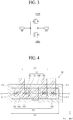
- the CMOS circuit may include a first transistor T1 having the P-type semiconductor characteristic and a second transistor T2 having the N-type semiconductor characteristic.
- a gate electrode of the first transistor T1 and a gate electrode of the second transistor T2 may be connected to an input terminal IT.
- a source electrode of the first transistor T1 may be connected to a driving voltage line VDD through which a driving voltage is supplied, and a drain electrode may be connected to an output terminal OT.
- a source electrode of the second transistor T2 may be connected to a ground GND, and a drain electrode may be connected to the output terminal OT.
- the first transistor T1 When a first logic level voltage is applied through the input terminal IT, the first transistor T1 may be turned on, and the second transistor T2 may be turned off. Therefore, the driving voltage of the driving voltage line VDD may be output to the output terminal OT through the first transistor T1.
- the second transistor T2 When a second logic level voltage having a level higher than that of the first logic level voltage is applied through the input terminal IT, the second transistor T2 may be turned on, and the first transistor T1 may be turned off. Therefore, the output terminal OT may be connected to the ground GND through the second transistor T2, and thus, the output terminal OT may be discharged to a ground voltage.
- the first transistor T1 may have the P-type semiconductor characteristic
- the second transistor T2 may have the N-type semiconductor characteristic
- the gate electrode of the first transistor T1 and the gate electrode of the second transistor T2 may be connected to the same input terminal, whereby the first transistor T1 and the second transistor T2 may be complementarily turned on and turned off in the CMOS circuit.
- the display device may include both of the P-type TFT and the N-type TFT for driving, but in this case, a manufacturing process is complicated.
- the CMOS circuit may be implemented with one transistor including a P-type semiconductor layer and a N-type semiconductor layer, or the P-type transistor or the N-type transistor may be selectively implemented, thereby preventing the manufacturing process from being complicated.
- a TFT implemented as a CMOS circuit will be described in detail with reference to FIGS. 4 to 10
- a TFT selectively implemented as one of a P-type transistor and a N-type transistor according to another embodiment of the present disclosure will be described in detail with reference to FIGS. 11 and 12 .
- FIG. 4 is a plan view illustrating a TFT 10 according to an embodiment of the present disclosure.
- FIG. 5 is a cross-sectional view taken along line I-I' of FIG. 4 .
- the TFT 10 according to an embodiment of the present disclosure is illustrated as being provided in a coplanar structure.
- the coplanar structure may have a top gate structure where a gate electrode is provided on an active layer.
- the TFT 10 may include a bottom gate electrode 110, a semiconductor layer 130, a first source electrode 141, a first drain electrode 142, a second source electrode 143, a second drain electrode 144, and a top gate electrode 160.
- the semiconductor layer 130 may include a N-type semiconductor layer 131 and a P-type semiconductor layer 132.
- the top gate electrode 160, the P-type semiconductor layer 132, the first source electrode 141, and the first drain electrode 142 may act as the first transistor T1 illustrated in FIG. 3
- the bottom gate electrode 110, the N-type semiconductor layer 131, the second source electrode 143, and the second drain electrode 144 may act as the second transistor T2 illustrated in FIG. 3
- the TFT 10 according to an embodiment of the present disclosure may include the N-type semiconductor layer 131 and the P-type semiconductor layer 132, and thus, may have both of the N-type semiconductor characteristic and the P-type semiconductor characteristic.
- the TFT 10 may be formed on a substrate 100.
- the substrate 100 may be formed of plastic, glass, and/or the like.
- a buffer layer may be formed on the substrate 100, for protecting the TFT 10 from water penetrating through the substrate 100.
- the buffer layer may include a plurality of inorganic layers which are alternately stacked.
- the buffer layer may be formed of a multilayer where one or more inorganic layers of silicon oxide (SiOx), silicon nitride (SiNx), and SiON are alternately stacked.
- the bottom gate electrode 110 of the TFT 10 may be formed on the substrate 100 or the buffer layer.
- the bottom gate electrode 110 may be formed of a single layer or a multilayer which includes one of molybdenum (Mo), aluminum (Al), chromium (Cr), gold (Au), titanium (Ti), nickel (Ni), neodymium (Nd), and copper (Cu), or an alloy thereof.
- a first gate insulation layer 120 may be formed on the bottom gate electrode 110.
- the first gate insulation layer 120 may be formed of an inorganic layer, and for example, may be formed of SiOx, SiNx, or a multilayer thereof.
- the bottom gate electrode 110 may block light which is incident on the N-type semiconductor layer 131 from the substrate 100. That is, the N-type semiconductor layer 131 may be protected by the bottom gate electrode 110 from the light.
- the semiconductor layer 130 may be formed on the first gate insulation layer 120.
- the semiconductor layer 130 may include the N-type semiconductor layer 131 and the P-type semiconductor layer 132.
- the N-type semiconductor layer 131 may be formed on the first gate insulation layer 120, and the P-type semiconductor layer 132 may be formed on the N-type semiconductor layer 131.
- the semiconductor layer 130 may overlap each of the bottom gate electrode 110 and the top gate electrode 160.
- the N-type semiconductor layer 131 may be formed as a N-type oxide semiconductor layer, and the P-type semiconductor layer 132 may be formed as a P-type oxide semiconductor layer. If the N-type semiconductor layer 131 is the N-type oxide semiconductor layer, the N-type semiconductor layer 131 may be formed of Indium Gallium Zinc Oxide (IGZO), Indium Zinc Oxide (IZO), Indium Gallium Oxide (IGO), Indium Tin Zinc Oxide (ITZO), Gallium Tin Oxide (GTO), Zinc Tin Oxide (ZTO), Indium Aluminum Zinc Oxide (IAZO), Aluminum Zinc Oxide (AZO), Indium Tin Oxide (ITO), Antimony Tin Oxide (ATO), Gallium Zinc Oxide (GZO), and/or the like.
- IGZO Indium Gallium Zinc Oxide
- IZO Indium Zinc Oxide
- IGO Indium Gallium Oxide
- ITZO Indium Tin Zinc Oxide
- GTO Gallium Tin Oxide
- ZTO Zinc
- a length L1 of the N-type semiconductor layer 131 in a first direction may be set longer than a length L2 of the P-type semiconductor layer 132 in the first direction (the X-axis direction). Therefore, a portion of the N-type semiconductor layer 131 may not be covered by the P-type semiconductor layer 132. Therefore, the second source electrode 143 and the second drain electrode 144 may be connected to the portion of the N-type semiconductor layer 131 uncovered by the P-type semiconductor layer 132.
- a length of the N-type semiconductor layer 131 in a second direction (a Y-axis direction) is set substantially equal to that of the P-type semiconductor layer 132 in the second direction (the Y-axis direction) is illustrated, but the present embodiment is not limited thereto. In other embodiments, the length of the N-type semiconductor layer 131 in the second direction (the Y-axis direction) may be set longer than that of the P-type semiconductor layer 132 in the second direction (the Y-axis direction).
- a second gate insulation layer 151 and a third gate insulation layer 152 may be formed on the P-type semiconductor layer 132.
- Each of the second gate insulation layer 151 and the third gate insulation layer 152 may be formed of an inorganic layer, and for example, may be formed of SiOx, SiNx, or a multilayer thereof.
- the third gate insulation layer 152 may be omitted.
- the top gate electrode 160 may be formed on the third gate insulation layer 152.
- the top gate electrode 160 may be formed of a single layer or a multilayer which includes one of Mo, Al, Cr, Au, Ti, Ni, Nd, and Cu, or an alloy thereof.
- a length of the top gate electrode 160 in the second direction (the Y-axis direction) is set longer than that of the P-type semiconductor layer 132 in the second direction (the Y-axis direction) is illustrated, but the present embodiment is not limited thereto. In other embodiments, the length of the top gate electrode 160 in the second direction (the Y-axis direction) may be set substantially equal to or shorter than that of the P-type semiconductor layer 132 in the second direction (the Y-axis direction).
- a channel region of the P-type semiconductor layer 132 may be widely provided, and thus, based on this, the length of the top gate electrode 160 in the second direction (the Y-axis direction) may be designed.
- An interlayer insulation layer 170 may be formed on the first gate insulation layer 120, the N-type semiconductor layer 131, the P-type semiconductor layer 132, and the top gate electrode 160.
- the interlayer insulation layer 170 may be formed of an inorganic layer, and for example, may be formed of SiOx, SiNx, or a multilayer thereof.
- a first contact hole C1 and a second contact hole C2, which pass through the interlayer insulation layer 170 to expose the P-type semiconductor layer 132, may be formed in the interlayer insulation layer 170
- a third contact hole C3 and a fourth contact hole C4, which pass through the interlayer insulation layer 170 to expose the N-type semiconductor layer 131, may be formed in the interlayer insulation layer 170.
- a portion of the N-type semiconductor layer 131 uncovered by the P-type semiconductor layer 132 may be exposed by the third contact hole C3 and the fourth contact hole C4.
- the first source electrode 141, the first drain electrode 142, the second source electrode 143, and the second drain electrode 144 may be formed on the interlayer insulation layer 170.
- the first source electrode 141 may be connected to the P-type semiconductor layer 132 through the first contact hole C1.
- the first drain electrode 142 may be connected to the P-type semiconductor layer 132 through the second contact hole C2.
- the second source electrode 143 may be connected to, through the third contact hole C3, the portion of the N-type semiconductor layer 131 uncovered by the P-type semiconductor layer 132.
- the second drain electrode 144 may be connected to, through the fourth contact hole C4, the portion of the N-type semiconductor layer 131 uncovered by the P-type semiconductor layer 132.
- the first contact hole C1 and the second contact hole C2 may be disposed between the third contact hole C3 and the fourth contact hole C4.
- the first source electrode 141 and the first drain electrode 142 may be connected to the P-type semiconductor layer 132 having a length shorter than that of the N-type semiconductor layer 131 in the first direction (the X-axis direction), and thus, an interval between the first source electrode 141 and the first drain electrode 142 may be shorter than an interval between the second source electrode 143 and the second drain electrode 144.
- the first drain electrode 142 may be connected to the second drain electrode 144, and in this case, the TFT 10 may function as a CMOS.
- FIG. 6 is a graph showing the N-type semiconductor characteristic and the P-type semiconductor characteristic of the TFT according to an embodiment of the present disclosure.
- FIGS. 7A and 7B are exemplary diagrams showing a hole concentration when the N-type semiconductor characteristic of the TFT according to an embodiment of the present disclosure is implemented and an electron concentration when the P-type semiconductor characteristic of the TFT is implemented.
- FIGS. 6 , 7A, and 7B an example where the N-type semiconductor layer 131 is formed of IGZO and the P-type semiconductor layer 132 is formed of Cu 2 O will be described below.
- FIG. 6 a current NIds which flows in the N-type semiconductor layer 131 with a voltage applied to the bottom gate electrode 110 and a current PIds which flows in the P-type semiconductor layer 132 with a voltage applied to the top gate electrode 160 are shown.
- the X axis represents a gate voltage Vg
- the Y axis represents a value of a current (hereinafter referred to as a current value) A.
- FIG. 7A shows a hole concentration when the gate voltage Vg is -10 V in FIG. 6 (i.e., the current PIds flowing in the P-type semiconductor layer 132 is saturated).
- FIG. 7B shows an electron concentration when the gate voltage Vg is +10 V in FIG. 6 (i.e., the current NIds flowing in the N-type semiconductor layer 131 is saturated).
- the gate voltage Vg applied to the bottom gate electrode 110 is a negative voltage, a current hardly flows in the N-type semiconductor layer 131. Also, if the gate voltage Vg applied to the bottom gate electrode 110 is a positive voltage, the current NIds flowing in the N-type semiconductor layer 131 increases in proportion to the gate voltage Vg. Also, if the current NIds flowing in the N-type semiconductor layer 131 is saturated as in FIG. 7B , the electron concentration is highest in a lower portion of the N-type semiconductor layer 131 close to the bottom gate electrode 110. Accordingly, it may be considered that the N-type semiconductor layer 131 has the N-type semiconductor characteristic.
- the gate voltage Vg applied to the top gate electrode 160 is a positive voltage, a current hardly flows in the P-type semiconductor layer 132. Also, if the gate voltage Vg applied to the top gate electrode 160 is a negative voltage, the current PIds flowing in the P-type semiconductor layer 132 increases as the gate voltage Vg is lowered. Also, if the current PIds flowing in the P-type semiconductor layer 132 is saturated as in FIG. 7A , the hole concentration is highest in the P-type semiconductor layer 132. Accordingly, it may be considered that the P-type semiconductor layer 132 has the P-type semiconductor characteristic.
- a thickness of the P-type semiconductor layer 132 may be set thinner than that of the N-type semiconductor layer 131.
- a carrier concentration of the N-type semiconductor layer 131 may be adjusted to about 5 ⁇ e 17 /cm 3
- a carrier concentration of the P-type semiconductor layer 132 may be adjusted to about 1 ⁇ e 18 /cm 3 .
- FIG. 8 is a graph showing the P-type semiconductor properties in accordance with the thickness of the P-type semiconductor layer.
- FIG. 8 shows the current value (Ids) of a p-type channel area in accordance with the gate-source voltage (Vgs), on assumption that a drain-source voltage is -20V, when the thickness of the P-type semiconductor layer 132 is 10 nm, 20 nm, or 30 nm and the thickness of the N-type semiconductor layer 131 is 30 nm.
- the X-axis indicates the gate-source voltage (Vgs)
- the Y-axis indicates the current value (Ids) of the p-type channel area.
- the P-type semiconductor layer 132 when the thickness of the P-type semiconductor layer 132 is 20 nm or 30 nm, the current continuously flows despite the change in the gate-source voltage (Vgs), so that it is difficult to realize the P-type semiconductor properties. That is, when the thickness of the P-type semiconductor layer 132 is 20 nm or 30 nm, the P-type semiconductor layer 132 does not have the P-type semiconductor properties.
- the off-current properties is shown when the gate-source voltage (Vgs) is near 0V. That is, if the thickness of the P-type semiconductor layer 132 is 10 nm, it is possible to realize the P-type semiconductor properties.
- the thin film transistor 10 may realize the P-type semiconductor properties when the thickness of the P-type semiconductor layer 132 may be less than the thickness of the N-type semiconductor layer 131.
- the N-type semiconductor layer 131 may be formed on the bottom gate electrode 110
- the P-type semiconductor layer 132 may be formed on the N-type semiconductor layer 131
- the top gate electrode 160 may be formed on the P-type semiconductor layer 132
- the length L1 of the N-type semiconductor layer 131 in the first direction (the X-axis direction) may be set longer than the length L2 of the P-type semiconductor layer 132 in the first direction (the X-axis direction).
- the first source electrode 141 and the first drain electrode 142 may be connected to the P-type semiconductor layer 132, and the second source electrode 143 and the second drain electrode 144 may be connected to a portion of the N-type semiconductor layer 131 uncovered by the P-type semiconductor layer 132.
- the N-type semiconductor layer 131 when a positive voltage is applied to the bottom gate electrode 110, the N-type semiconductor layer 131 may be configured to have the N-type semiconductor characteristic, and when a negative voltage is applied to the top gate electrode 160, the P-type semiconductor layer 132 may be configured to have the P-type semiconductor characteristic.
- FIG. 9 is a flowchart illustrating a method of manufacturing a TFT according to an embodiment of the present disclosure.
- FIGS. 10A to 10F are cross-sectional views for describing a method of manufacturing a TFT according to an embodiment of the present disclosure.
- FIGS. 10A to 10F relate to a method of manufacturing the TFT illustrated in FIG. 4 , and thus, like reference numerals refer to like elements.
- a method of manufacturing a TFT according to an embodiment of the present disclosure will be described in detail with reference to FIGS. 9 and 10A to 10F .
- the method of manufacturing a thin film transistor comprises: forming a bottom gate electrode on a substrate; forming a semiconductor layer overlapping with the bottom gate electrode, wherein the semiconductor layer comprises a N-type semiconductor layer and a P-type semiconductor layer, and the N-type semiconductor layer is overlapped partly with the P-type semiconductor layer; forming a first source electrode and a first drain electrode respectively connected to the P-type semiconductor layer; forming a second source electrode and a second drain electrode respectively connected to a portion of the N-type semiconductor layer which is not overlapped with the P-type semiconductor layer; and forming a top gate electrode above the semiconductor layer.
- a bottom gate electrode 110 may be formed on a substrate 100.
- a first metal layer may be formed on a whole upper surface of the substrate 100 through a sputtering process.
- a photoresist pattern may be formed on the first metal layer, and then, by patterning the first metal layer through a mask process of etching the first metal layer, the bottom gate electrode 110 may be formed.
- the bottom gate electrode 110 may be formed of a single layer or a multilayer which includes one of Mo, Al, Cr, Au, Ti, Ni, Nd, and Cu, or an alloy thereof.
- a buffer layer may be formed on the substrate 100, for protecting a TFT 10 from water penetrating through the substrate 100.
- the bottom gate electrode 110 may be formed on the buffer layer.
- the buffer layer may include a plurality of inorganic layers which are alternately stacked.
- the buffer layer may be formed of a multilayer where one or more inorganic layers of SiOx, SiNx, and SiON are alternately stacked.
- the buffer layer may be formed through a plasma enhanced chemical vapor deposition (PECVD) process. (S101 of FIG. 9 )
- a first gate insulation layer 120 may be formed on the bottom gate electrode 110.
- the first gate insulation layer 120 may be formed of an inorganic layer, and for example, may be formed of SiOx, SiNx, or a multilayer thereof.
- the first gate insulation layer 120 may be formed through a PECVD process.
- a semiconductor layer 130 including a N-type semiconductor layer 131 and a P-type semiconductor layer 132 may be formed on the first gate insulation layer 120.
- a first semiconductor layer may be formed on a whole upper surface of the first gate insulation layer 120, and then, a second semiconductor layer may be formed on a whole upper surface of the first semiconductor layer.
- the N-type semiconductor layer 131 and the P-type semiconductor layer 132 may be formed by simultaneously patterning the first and second semiconductor layers through a mask process using a photoresist pattern.
- the N-type semiconductor layer 131 may overlap the bottom gate electrode 110.
- the N-type semiconductor layer 131 and the P-type semiconductor layer 132 may each be formed as an oxide semiconductor layer.
- the N-type semiconductor layer 131 may be formed of IGZO, IZO, IGO, ITZO, GTO, ZTO, IAZO, AZO, ITO, ATO, GZO, and/or the like
- the P-type semiconductor layer 132 is formed of Cu 2 O will be described.
- the N-type semiconductor layer 131 and the P-type semiconductor layer 132 should be formed under a condition where a vacuum state is maintained, in order for the TFT 10 to have both of the N-type semiconductor characteristic and the P-type semiconductor characteristic. That is, the N-type semiconductor layer 131 and the P-type semiconductor layer 132 may be continuously deposited in one chamber while the vacuum state is being maintained. For example, a vacuum of 5 mTorr to 10 mTorr may be maintained when forming the N-type semiconductor layer 131 and the P-type semiconductor layer 132.
- the N-type semiconductor layer 131 can be oxidized by oxygen in the atmosphere. In this case, an interface between the N-type semiconductor layer 131 and the P-type semiconductor layer 132 can be unstable. Also, if the vacuum state is not maintained when forming the N-type semiconductor layer 131 and the P-type semiconductor layer 132, the P-type semiconductor layer 132 can be formed of CuO instead of Cu 2 O, due to oxygen in the atmosphere.
- an oxygen tension may be adjusted to 3% or less. In this case, if the oxygen tension exceeds 3%, the P-type semiconductor layer 132 may be formed of CuO instead of Cu 2 O. Also, in a case where the P-type semiconductor layer 132 is formed through an O 2 reaction by using Cu as a target, the oxygen tension may be adjusted to 40% or more.
- the P-type semiconductor layer 132 is formed of CuO
- electron mobility is more reduced than a case where the P-type semiconductor layer 132 is formed of Cu 2 O. That is, in a case where the P-type semiconductor layer 132 is formed of CuO, an electron mobility of the P-type semiconductor layer 132 may be 1 cm 2 /Vs or less and may be very low. For this reason, the TFT 10 is difficult to realize the P-type semiconductor characteristic.
- thermal treatment may be performed at a high temperature.
- thermal treatment may be performed on the P-type semiconductor layer 132 including CuO for 30 minutes or more at a high temperature of 300 degrees C or more in a vacuum state.
- oxygen is desorbed from the N-type semiconductor layer 131, and thus, a conductivity of the N-type semiconductor layer 131 increases. Therefore, even when a gate voltage Vg applied to the bottom gate electrode 110 is a negative voltage, a current NIds can flow in the N-type semiconductor layer 131. That is, a problem where an off current increases can occur.
- the N-type semiconductor layer 131 may be formed in a state where oxygen is plentiful. For example, when forming the N-type semiconductor layer 131, an oxygen tension may be adjusted to 3% to 10%. However, based on a material of the N-type semiconductor layer 131, if it is required to enhance electron mobility, the oxygen tension necessary for forming the N-type semiconductor layer 131 may be adjusted to 0% to 3%.
- the N-type semiconductor layer 131 may have a thickness of 30 nm or less, for enhancing electron mobility. Also, in a case where a thickness of the P-type semiconductor layer 132 is adjusted to 10 nm or less, the turn-off of a p-type channel region is controlled as shown in FIG. 8 , and moreover, the P-type semiconductor layer 132 is easily formed of Cu 2 O. Therefore, the thickness of the P-type semiconductor layer 132 maybe adjusted to 10 nm or less. (S102 of FIG. 9 )
- a second gate insulation layer 151 may be formed to cover a portion of the P-type semiconductor layer 132, and a portion of the P-type semiconductor layer 132 uncovered by the second gate insulation layer 151 may be etched by using the second gate insulation layer 151 as a passivation layer. Therefore, a length L1 of the N-type semiconductor layer 131 in a first direction (an X-axis direction) may be set longer than a length L2 of the P-type semiconductor layer 132 in the first direction (the X-axis direction). (S103 of FIG. 9 )
- a third gate insulation layer 152 may be formed on the second gate insulation layer 151, and a top gate electrode 160 may be formed on the third gate insulation layer 152.
- the third gate insulation layer 152 may be formed on a whole upper surface of the second gate insulation layer 151 through a PECVD process. Subsequently, a second metal layer may be formed on a whole upper surface of the third gate insulation layer 152 through a sputtering process or an MOCVD process. Subsequently, the second gate insulation layer 151, the third gate insulation layer 152, and the top gate electrode 160 may be finished by simultaneously patterning the second gate insulation layer 151, the third gate insulation layer 152, and the second metal layer through a mask process using a photoresist pattern. The top gate electrode 160 may overlap the P-type semiconductor layer 132. The third gate insulation layer 152 may be omitted. (S104 of FIG. 9 )
- an interlayer insulation layer 170 may be formed on the N-type semiconductor layer 131, the P-type semiconductor layer 132, and the top gate electrode 160.
- the interlayer insulation layer 170 may be formed through a PECVD process.
- a first contact hole C1 and a second contact hole C2, which pass through the interlayer insulation layer 170 to expose the P-type semiconductor layer 132, may be formed, and a third contact hole C3 and a fourth contact hole C4, which expose a portion of the N-type semiconductor layer 131 uncovered by the P-type semiconductor layer 132, may be formed.
- first and second source electrodes 141 and 143 and first and second drain electrodes 142 and 144 may be formed on the interlayer insulation layer 170.
- a third metal layer may be formed on a whole upper surface of the interlayer insulation layer 170 through a sputtering process or an MOCVD process. Subsequently, the first and second source electrodes 141 and 143 and the first and second drain electrodes 142 and 144 may be formed by patterning the third metal layer through a mask process using a photoresist pattern.
- the first source electrode 141 may be connected to the P-type semiconductor layer 132 through the first contact hole C1.
- the first drain electrode 142 may be connected to the P-type semiconductor layer 132 through the second contact hole C2.
- the second source electrode 143 may be connected to, through the third contact hole C3, a portion of the N-type semiconductor layer 131 uncovered by the P-type semiconductor layer 132.
- the second drain electrode 144 may be connected to, through the fourth contact hole C4, the portion of the N-type semiconductor layer 131 uncovered by the P-type semiconductor layer 132.
- the first drain electrode 142 may be connected to the second drain electrode 144, and in this case, the TFT 10 may function as a CMOS.
- the first and second source electrodes 141 and 143 and the first and second drain electrodes 142 and 144 may each be formed of a single layer or a multilayer which includes one of Mo, Al, Cr, Au, Ti, Ni, Nd, and Cu, or an alloy thereof.
- the first source electrode 141 and the first drain electrode 142 may be connected to the P-type semiconductor layer 132, and thus, based on this, the first source electrode 141 and the first drain electrode 142 may each be formed of a single layer or a multilayer which includes one of palladium (Pd) having a work function of 5.22 eV to 5.6 eV, platinum (Pt) having a work function of 5.12 eV to 5.93 eV, gold (Au) having a work function of 5.1 eV to 5.47 eV, and nickel (Ni) having a work function of 5.04 eV to 5.35 eV, which have a work function higher than 5.0 eV, or an alloy thereof.
- Pd palladium
- Pt platinum
- Au gold
- Au gold
- Ni nickel
- the N-type semiconductor layer 131 and the P-type semiconductor layer 132 may be formed through a continuous deposition process in one chamber while maintaining a vacuum state.
- an interface between the N-type semiconductor layer 131 and the P-type semiconductor layer 132 may be stably formed, and moreover, the N-type semiconductor layer 131 and the P-type semiconductor layer 132 may each be formed of Cu 2 O instead of CuO. That is, according to an embodiment of the present disclosure, a TFT which includes the N-type semiconductor layer 131 having the N-type semiconductor characteristic and the P-type semiconductor layer 132 having the P-type semiconductor characteristic may be manufactured.
- FIG. 11 is a plan view illustrating a TFT 10 according to another embodiment of the present disclosure.
- FIG. 12 is a cross-sectional view taken along line II-II' of FIG. 11 .
- the TFT 10 according to another embodiment of the present disclosure is illustrated as being provided in a coplanar structure.
- the coplanar structure may have a top gate structure where a gate electrode is provided on an active layer.
- the TFT 10 may include a P-type TFT PT having the P-type semiconductor characteristic and a N-type TFT NT having the N-type semiconductor characteristic.
- the P-type TFT PT may include a first bottom gate electrode 111, a first semiconductor layer 230, a first source electrode 141, a first drain electrode 142, and a first top gate electrode 161.
- the first semiconductor layer 230 may include a first N-type semiconductor layer 133 and a first P-type semiconductor layer 134.
- the TFT 10 is selectively implemented as a P-type TFT.
- a voltage may not be applied to the first bottom gate electrode 111, and thus, the first bottom gate electrode 111 may act as a light blocking layer which blocks light incident on the first N-type semiconductor layer 133 through a substrate 100.
- the N-type TFT NT may include a second bottom gate electrode 112, a second semiconductor layer 240, a second source electrode 143, a second drain electrode 144, and a second top gate electrode 162.
- the second semiconductor layer 240 may include a second N-type semiconductor layer 135 and a second P-type semiconductor layer 136.
- the TFT 10 is selectively implemented as a N-type TFT.
- a voltage may not be applied to the second top gate electrode 162, and thus, the second top gate electrode 162 may be omitted.
- the TFT 10 may be formed on the substrate 100.
- the substrate 100 may be formed of plastic, glass, and/or the like.
- a buffer layer may be formed on the substrate 100, for protecting the TFT 10 from water penetrating through the substrate 100.
- the buffer layer may include a plurality of inorganic layers which are alternately stacked.
- the buffer layer may be formed of a multilayer where one or more inorganic layers of SiOx, SiNx, and SiON are alternately stacked.
- the first bottom gate electrode 111 and the second bottom gate electrode 112 may be formed on the substrate 100 or the buffer layer.
- the first bottom gate electrode 111 and the second bottom gate electrode 112 may each be formed of a single layer or a multilayer which includes one of Mo, Al, Cr, Au, Ti, Ni, Nd, and Cu, or an alloy thereof.
- a first gate insulation layer 120 may be formed on the first bottom gate electrode 111 and the second bottom gate electrode 112.
- the first gate insulation layer 120 may be formed of an inorganic layer, and for example, may be formed of SiOx, SiNx, or a multilayer thereof.
- the first bottom gate electrode 111 and the second bottom gate electrode 112 may block light which is incident on the first and second N-type semiconductor layers 133 and 135 from the substrate 100. That is, the first and second N-type semiconductor layers 133 and 135 may be protected by the first bottom gate electrode 111 and the second bottom gate electrode 112 from the light.
- the first N-type semiconductor layer 133 and the second N-type semiconductor layer 135 may be formed on the first gate insulation layer 120.
- the first P-type semiconductor layer 134 may be formed on the first N-type semiconductor layer 133
- the second P-type semiconductor layer 136 may be formed on the second N-type semiconductor layer 135.
- the first N-type semiconductor layer 133 and the first P-type semiconductor layer 134 may overlap the first bottom gate electrode 111 and the first top gate electrode 161.
- the second N-type semiconductor layer 135 and the second P-type semiconductor layer 136 may overlap the second bottom gate electrode 112.
- the first N-type semiconductor layer 133 and the second N-type semiconductor layer 135 may each be formed as a N-type oxide semiconductor layer, and the first P-type semiconductor layer 134 and the second P-type semiconductor layer 136 may each be formed as a P-type oxide semiconductor layer. If each of the first N-type semiconductor layer 133 and the second N-type semiconductor layer 135 is the N-type oxide semiconductor layer, the first N-type semiconductor layer 133 and the second N-type semiconductor layer 135 may be formed of IGZO, IZO, IGO, ITZO, GTO, ZTO, IAZO, AZO, ITO, ATO, GZO, and/or the like.
- a thickness of each of the first P-type semiconductor layer 134 and the second P-type semiconductor layer 136 may be set thinner than that of each of the first N-type semiconductor layer 133 and the second N-type semiconductor layer 135. Particularly, in order to normally realize the P-type semiconductor characteristic, a thickness of each of the first P-type semiconductor layer 134 and the second P-type semiconductor layer 136 may be adjusted to 10 nm or less.
- a length L3 of the second N-type semiconductor layer 135 in a first direction may be set longer than a length L4 of the second P-type semiconductor layer 136 in the first direction (the X-axis direction). Therefore, a portion of the second N-type semiconductor layer 135 may not be covered by the second P-type semiconductor layer 136. Therefore, the second source electrode 143 and the second drain electrode 144 may be connected to the portion of the second N-type semiconductor layer 135 uncovered by the second P-type semiconductor layer 136.
- FIG. 11 an example where a length of the first N-type semiconductor layer 133 in the first direction (the X-axis direction) is set substantially equal to that of the first P-type semiconductor layer 134 in the first direction (the X-axis direction) is illustrated, but the present embodiment is not limited thereto. In other embodiments, the length of the first N-type semiconductor layer 133 in the first direction (the X-axis direction) may be set longer than that of the first P-type semiconductor layer 134 in the first direction (the X-axis direction).
- a length of the first N-type semiconductor layer 133 in a second direction (a Y-axis direction) is set substantially equal to that of the first P-type semiconductor layer 134 in the second direction (the Y-axis direction) is illustrated, but the present embodiment is not limited thereto. In other embodiments, the length of the first N-type semiconductor layer 133 in the second direction (the Y-axis direction) may be set longer than that of the first P-type semiconductor layer 134 in the second direction (the Y-axis direction).
- a length of the second N-type semiconductor layer 135 in the second direction is set substantially equal to that of the second P-type semiconductor layer 136 in the second direction (the Y-axis direction) is illustrated, but the present embodiment is not limited thereto. In other embodiments, the length of the second N-type semiconductor layer 135 in the second direction (the Y-axis direction) may be set longer than that of the second P-type semiconductor layer 136 in the second direction (the Y-axis direction).
- a second gate insulation layer 151 and a third gate insulation layer 152 may be formed on the first P-type semiconductor layer 134 and the second P-type semiconductor layer 136.
- Each of the second gate insulation layer 151 and the third gate insulation layer 152 may be formed of an inorganic layer, and for example, may be formed of SiOx, SiNx, or a multilayer thereof.
- the third gate insulation layer 152 may be omitted.
- the first top gate electrode 161 and the second top gate electrode 162 may be formed on the third gate insulation layer 152.
- the first top gate electrode 161 and the second top gate electrode 162 may each be formed of a single layer or a multilayer which includes one of Mo, Al, Cr, Au, Ti, Ni, Nd, and Cu, or an alloy thereof.
- FIG. 11 an example where a length of the first top gate electrode 161 in the second direction (the Y-axis direction) is set longer than that of the first P-type semiconductor layer 134 in the second direction (the Y-axis direction) is illustrated, but the present embodiment is not limited thereto. In other embodiments, the length of the first top gate electrode 161 in the second direction (the Y-axis direction) may be set substantially equal to or shorter than that of the first P-type semiconductor layer 134 in the second direction (the Y-axis direction).
- a channel region of the first P-type semiconductor layer 134 may be widely provided, and thus, based on this, the length of the first top gate electrode 161 in the second direction (the Y-axis direction) may be designed.
- the length of the second top gate electrode 162 in the second direction may be set substantially equal to or shorter than that of the second P-type semiconductor layer 136 in the second direction (the Y-axis direction).
- a channel region of the second P-type semiconductor layer 136 may be widely provided, and thus, based on this, the length of the second top gate electrode 162 in the second direction (the Y-axis direction) may be designed.
- An interlayer insulation layer 170 may be formed on the first gate insulation layer 120, the first N-type semiconductor layer 133, the first P-type semiconductor layer 134, the second N-type semiconductor layer 135, the second P-type semiconductor layer 136, and the first top gate electrode 161.
- the interlayer insulation layer 170 may be formed of an inorganic layer, and for example, may be formed of SiOx, SiNx, or a multilayer thereof.
- a first contact hole C1 and a second contact hole C2, which pass through the interlayer insulation layer 170 to expose the first P-type semiconductor layer 134, may be formed in the interlayer insulation layer 170, and a third contact hole C3 and a fourth contact hole C4, which pass through the interlayer insulation layer 170 to expose the second N-type semiconductor layer 135, may be formed in the interlayer insulation layer 170.
- a portion of the second N-type semiconductor layer 135 uncovered by the second P-type semiconductor layer 136 may be exposed by the third contact hole C3 and the fourth contact hole C4.
- the first source electrode 141, the first drain electrode 142, the second source electrode 143, and the second drain electrode 144 may be formed on the interlayer insulation layer 170.
- the first source electrode 141 may be connected to the first P-type semiconductor layer 134 through the first contact hole C1.
- the first drain electrode 142 may be connected to the first P-type semiconductor layer 134 through the second contact hole C2.
- the second source electrode 143 may be connected to, through the third contact hole C3, the portion of the second N-type semiconductor layer 135 uncovered by the second P-type semiconductor layer 136.
- the second drain electrode 144 may be connected to, through the fourth contact hole C4, the portion of the second N-type semiconductor layer 135 uncovered by the second P-type semiconductor layer 136.
- the second contact hole C2 and the fourth contact hole C4 are disposed between the first contact hole C1 and the third contact hole C3.
- the first source electrode 141 and the first drain electrode 142 may be connected to the first P-type semiconductor layer 134, and the second source electrode 143 and the second drain electrode 144 may be connected to the second N-type semiconductor layer 135. Accordingly, an interval between the first source electrode 141 and the first drain electrode 142 may be shorter than an interval between the second source electrode 143 and the second drain electrode 144. That is to say, a distance between the first contact hole C1 and the second contact hole C2 is shorter than a distance between the third contact hole C3 and the fourth contact hole C4.
- the first drain electrode 142 may be connected to the second drain electrode 144, and in this case, the TFT 10 may function as a CMOS.
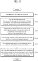
- FIG. 13 is a flowchart illustrating a method of manufacturing a TFT according to another embodiment of the present disclosure.
- FIGS. 14A to 14F are cross-sectional views for describing a method of manufacturing a TFT according to another embodiment of the present disclosure.
- FIGS. 14A to 14F relate to a method of manufacturing the TFT illustrated in FIG. 13 , and thus, like reference numerals refer to like elements.
- a method of manufacturing a TFT according to another embodiment of the present disclosure will be described in detail with reference to FIGS. 13 and 14A to 14F .
- the method of manufacturing a thin film transistor comprises: forming a first bottom gate electrode and a second bottom gate electrode on a substrate; forming a first semiconductor layer overlapping with the first bottom gate electrode and a second semiconductor layer overlapping with the second bottom gate electrode, wherein the second semiconductor layer comprises a second N-type semiconductor layer and a second P-type semiconductor layer, and the second N-type semiconductor layer is overlapped partly with the second P-type semiconductor layer; forming a first source electrode and a first drain electrode respectively connected to the first semiconductor layer; forming a second source electrode and a second drain electrode respectively connected to a portion of the second N-type semiconductor layer which is not overlapped with the second P-type semiconductor layer; and forming a first top gate electrode on the first semiconductor layer.
- a first bottom gate electrode 111 and a second bottom gate electrode 112 may be formed on a substrate 100.
- Step S201 of FIG. 13 is substantially the same as step S101 of FIG. 9 , and thus, its detailed description is omitted. (S201 of FIG. 13 )
- a first gate insulation layer 120 may be formed on the first bottom gate electrode 111 and the second bottom gate electrode 112
- a first N-type semiconductor layer 133 and a second N-type semiconductor layer 135 may be formed on the first gate insulation layer 120
- a first P-type semiconductor layer 134 may be formed on the first N-type semiconductor layer 133
- a second P-type semiconductor layer 136 may be formed on the second N-type semiconductor layer 135.
- Step S202 of FIG. 13 is substantially the same as step S102 of FIG. 9 , and thus, its detailed description is omitted. (S202 of FIG. 13 )
- a second gate insulation layer 151 may be formed to cover a whole portion of the first P-type semiconductor layer 134 and a portion of the second P-type semiconductor layer 136, and a portion of the second P-type semiconductor layer 136 uncovered by the second gate insulation layer 151 may be etched by using the second gate insulation layer 151 as a passivation layer. Therefore, a length L3 of the second N-type semiconductor layer 135 in a first direction (an X-axis direction) may be set longer than a length L4 of the second P-type semiconductor layer 136 in the first direction (the X-axis direction). (S203 of FIG. 13 )
- a third gate insulation layer 152 may be formed on the second gate insulation layer 151, and a top gate electrode 160 may be formed on the third gate insulation layer 152.
- the third gate insulation layer 152 may be formed on a whole upper surface of the second gate insulation layer 151 through a PECVD process. Subsequently, a second metal layer may be formed on a whole upper surface of the third gate insulation layer 152 through a sputtering process or an MOCVD process. Subsequently, the second gate insulation layer 151, the third gate insulation layer 152, the first top gate electrode 161, and the second top gate electrode 162 may be finished by simultaneously patterning the second gate insulation layer 151, the third gate insulation layer 152, and the second metal layer through a mask process using a photoresist pattern.
- the first top gate electrode 161 may overlap the first P-type semiconductor layer 134, and the second top gate electrode 162 may overlap the second P-type semiconductor layer 136.
- the second top gate electrode 162 and the third gate insulation layer 152 may be omitted. (S204 of FIG. 13 )
- an interlayer insulation layer 170 may be formed on the first N-type semiconductor layer 131, the first P-type semiconductor layer 134, the second N-type semiconductor layer 135, the second P-type semiconductor layer 136, the first top gate electrode 161, and the second top gate electrode 162.
- the interlayer insulation layer 170 may be formed through a PECVD process.
- a first contact hole C1 and a second contact hole C2, which pass through the interlayer insulation layer 170 to expose the first P-type semiconductor layer 134, may be formed, and a third contact hole C3 and a fourth contact hole C4, which expose a portion of the first N-type semiconductor layer 135 uncovered by the second P-type semiconductor layer 136, may be formed. (S205 of FIG. 13 )
- first and second source electrodes 141 and 143 and first and second drain electrodes 142 and 144 may be formed on the interlayer insulation layer 170.
- a third metal layer may be formed on a whole upper surface of the interlayer insulation layer 170 through atg sputtering process or an MOCVD process. Subsequently, the first and second source electrodes 141 and 143 and the first and second drain electrodes 142 and 144 may be formed by patterning the third metal layer through a mask process using a photoresist pattern.
- the first source electrode 141 may be connected to the first P-type semiconductor layer 134 through the first contact hole C1.
- the first drain electrode 142 may be connected to the first P-type semiconductor layer 134 through the second contact hole C2.
- the second source electrode 143 may be connected to, through the third contact hole C3, a portion of the second N-type semiconductor layer 135 uncovered by the second P-type semiconductor layer 136.
- the second drain electrode 144 may be connected to, through the fourth contact hole C4, the portion of the second N-type semiconductor layer 135 uncovered by the second P-type semiconductor layer 136.
- the first drain electrode 142 may be connected to the second drain electrode 144, and in this case, the TFT 10 may function as a CMOS.
- the first and second source electrodes 141 and 143 and the first and second drain electrodes 142 and 144 may each be formed of a single layer or a multilayer which includes one of Mo, Al, Cr, Au, Ti, Ni, Nd, and Cu, or an alloy thereof.
- the first source electrode 141 and the first drain electrode 142 may be connected to the first P-type semiconductor layer 134, and thus, based on this, the first source electrode 141 and the first drain electrode 142 may each be formed of a single layer or a multilayer which includes one of Pd having a work function of 5.22 eV to 5.6 eV, Pt having a work function of 5.12 eV to 5.93 eV, Au having a work function of 5.1 eV to 5.47 eV, and Ni having a work function of 5.04 eV to 5.35 eV, which have a work function higher than 5.0 eV, or an alloy thereof. (S206 of FIG. 13 )
- the CMOS circuit may be implemented with one transistor including the P-type semiconductor layer and the N-type semiconductor layer, or the P-type transistor or the N-type transistor may be selectively implemented. Accordingly, a manufacturing process is not complicated.
Landscapes
- Engineering & Computer Science (AREA)
- Physics & Mathematics (AREA)
- General Physics & Mathematics (AREA)
- Computer Hardware Design (AREA)
- Theoretical Computer Science (AREA)
- Microelectronics & Electronic Packaging (AREA)
- Crystallography & Structural Chemistry (AREA)
- Chemical & Material Sciences (AREA)
- Nonlinear Science (AREA)
- Geometry (AREA)
- Mathematical Physics (AREA)
- Optics & Photonics (AREA)
- Thin Film Transistor (AREA)
- Liquid Crystal (AREA)
- Electroluminescent Light Sources (AREA)
- Devices For Indicating Variable Information By Combining Individual Elements (AREA)
Abstract
Description
- The present disclosure relates to a thin film transistor (TFT) and a display device including the TFT.
- With the advancement of information-oriented society, various requirements for display devices for displaying an image are increasing. Recently, various flat panel display devices such as liquid crystal display (LCD) devices, plasma display panel (PDP) devices, and organic light emitting display devices are being practically used.
- Flat panel display devices, such as LCD devices and organic light emitting display devices, each include a display panel, a gate driving circuit, a data driving circuit, and a timing controller. The display panel includes a plurality of data lines, a plurality of gate lines, and a plurality of pixels which are respectively provided in a plurality of pixel areas defined by intersections of the data lines and the gate lines and are supplied with data voltages of the data lines when gate signals are supplied to the gate lines. The pixels emit light having certain brightness with the data voltages.
- Moreover, the flat panel display devices drive the pixels and the gate driving circuit by using TFTs as switching elements. The pixels and/or the gate driving circuit of each of the flat panel display devices may include a N-type TFT having a N-type semiconductor characteristic and a P-type TFT having a P-type semiconductor characteristic. The N-type TFT and the P-type TFT may each be a metal oxide semiconductor field effect transistor (MOSFET) which controls a flow of a current with an electric field.
- If the flat panel display devices each include a N-type oxide semiconductor transistor and a P-type oxide semiconductor transistor, a manufacturing process is complicated. For example, in a case where a N-type semiconductor layer is formed and then a P-type semiconductor layer is formed, the N-type semiconductor layer may need to be etched when patterning the P-type semiconductor layer. In order to solve such a problem, a passivation layer for protecting the N-type semiconductor layer is formed, and after the P-type semiconductor layer is patterned, the passivation layer is removed. That is, in a case where the flat panel display devices each include both of the N-type oxide semiconductor transistor and the P-type oxide semiconductor transistor, in addition to a process of forming the N-type semiconductor layer or the P-type semiconductor layer, a process of forming and removing the passivation layer may be additionally performed in comparison with a case where the flat panel display devices each include one of the N-type oxide semiconductor transistor and the P-type oxide semiconductor transistor.
- Accordingly, the present disclosure is directed to provide a TFT and a display device including the TFT that substantially obviate one or more problems due to limitations and disadvantages of the related art.
- An aspect of the present disclosure is directed to provide a TFT including a N-type semiconductor layer and a P-type semiconductor layer, a method of manufacturing the same, and a display device including the TFT, in which a complexity of a manufacturing process is reduced.
- Additional advantages and features of the disclosure will be set forth in part in the description which follows and in part will become apparent to those having ordinary skill in the art upon examination of the following or may be learned from practice of the disclosure. The objectives and other advantages of the disclosure may be realized and attained by the structure particularly pointed out in the written description and claims hereof as well as the appended drawings.
- To achieve these and other advantages and in accordance with the purpose of the disclosure, as embodied and broadly described herein, there is provided a TFT comprising: a bottom gate electrode on a substrate; a semiconductor layer overlapping with the bottom gate electrode, wherein the semiconductor layer comprises a N-type semiconductor layer and a P-type semiconductor layer, and the N-type semiconductor layer is overlapped partly with the P-type semiconductor layer; a first source electrode and a first drain electrode respectively connected to the P-type semiconductor layer; a second source electrode and a second drain electrode respectively connected to a portion of the N-type semiconductor layer which is not overlapped with the P-type semiconductor layer; and a top gate electrode above the semiconductor layer.
- There is provided a display device including a thin film transistor, wherein the display device comprises: a display panel; a data driving circuit; and a gate driving circuit, wherein the display panel or the gate driving circuit comprises a thin film transistor and the thin film transistor comprising: a bottom gate electrode on a substrate; a semiconductor layer overlapping with the bottom gate electrode, wherein the semiconductor layer comprises a N-type semiconductor layer and a P-type semiconductor layer, and the N-type semiconductor layer is overlapped partly with the P-type semiconductor layer; a first source electrode and a first drain electrode respectively connected to the P-type semiconductor layer; a second source electrode and a second drain electrode respectively connected to a portion of the N-type semiconductor layer which is not overlapped with the P-type semiconductor layer; and a top gate electrode above the semiconductor layer.
- There is provided a TFT comprising a first bottom gate electrode and a second bottom gate electrode on a substrate; a first semiconductor layer overlapping with the first bottom gate electrode and a second semiconductor layer overlapping with the second bottom gate electrode, wherein the second semiconductor layer comprises a second N-type semiconductor layer and a second P-type semiconductor layer, and the second N-type semiconductor layer is overlapped partly with the second P-type semiconductor layer; a first source electrode and a first drain electrode respectively connected to the first semiconductor layer; a second source electrode and a second drain electrode respectively connected to a portion of the second N-type semiconductor layer which is not overlapped with the second P-type semiconductor layer; and a first top gate electrode on the first semiconductor layer.
- There is provided a display device including a thin film transistor, wherein the display device comprises: a display panel; a data driving circuit; and a gate driving circuit, wherein the display panel or the gate driving circuit comprises a thin film transistor and the thin film transistor comprising: a first bottom gate electrode and a second bottom gate electrode on a substrate; a first semiconductor layer overlapping with the first bottom gate electrode and a second semiconductor layer overlapping with the second bottom gate electrode, wherein the second semiconductor layer comprises a second N-type semiconductor layer and a second P-type semiconductor layer, and the second N-type semiconductor layer is overlapped partly with the second P-type semiconductor layer; a first source electrode and a first drain electrode respectively connected to the first semiconductor layer; a second source electrode and a second drain electrode respectively connected to a portion of the second N-type semiconductor layer which is not overlapped with the second P-type semiconductor layer; and a first top gate electrode on the first semiconductor layer.
- It is to be understood that both the foregoing general description and the following detailed description of the present disclosure are exemplary and explanatory and are intended to provide further explanation of the disclosure as claimed.
- The accompanying drawings, which are included to provide a further understanding of the disclosure and are incorporated in and constitute a part of this application, illustrate embodiments of the disclosure and together with the description serve to explain the principle of the disclosure. In the drawings:
-
FIG. 1 is a perspective view illustrating a display device according to an embodiment of the present disclosure; -
FIG. 2 is a plan view illustrating a first substrate, a gate driver, a source drive integrated circuit (IC), a flexible film, a circuit board, and a timing controller illustrated inFIG. 1 ; -
FIG. 3 is a circuit diagram illustrating a complementary metal oxide semiconductor (CMOS) circuit; -
FIG. 4 is a plan view illustrating a TFT according to an embodiment of the present disclosure; -
FIG. 5 is a cross-sectional view taken along line I-I' ofFIG. 4 ; -
FIG. 6 is a graph showing a N-type semiconductor characteristic and a P-type semiconductor characteristic of a TFT according to an embodiment of the present disclosure; -
FIGS. 7A and 7B are exemplary diagrams showing a hole concentration when a N-type semiconductor characteristic of a TFT according to an embodiment of the present disclosure is implemented and an electron concentration when a P-type semiconductor characteristic of the TFT is implemented; -
FIG. 8 is a graph showing the P-type semiconductor properties in accordance with the thickness of the P-type semiconductor layer; -
FIG. 9 is a flowchart illustrating a method of manufacturing a TFT according to an embodiment of the present disclosure; -
FIGS. 10A to 10F are cross-sectional views for describing a method of manufacturing a TFT according to an embodiment of the present disclosure; -
FIG. 11 is a plan view illustrating a TFT according to another embodiment of the present disclosure; -
FIG. 12 is a cross-sectional view taken along line II-II' ofFIG. 10 ; -
FIG. 13 is a flowchart illustrating a method of manufacturing a TFT according to another embodiment of the present disclosure; and -
FIGS. 14A to 14F are cross-sectional views for describing a method of manufacturing a TFT according to another embodiment of the present disclosure. - Reference will now be made in detail to the exemplary embodiments of the present disclosure, examples of which are illustrated in the accompanying drawings. Wherever possible, the same reference numbers will be used throughout the drawings to refer to the same or like parts.
- In the specification, it should be noted that like reference numerals already used to denote like elements in other drawings are used for elements wherever possible. In the following description, when a function and a configuration known to those skilled in the art are irrelevant to the essential configuration of the present disclosure, their detailed descriptions will be omitted. The terms described in the specification should be understood as follows.
- Advantages and features of the present disclosure, and implementation methods thereof will be clarified through following embodiments described with reference to the accompanying drawings. The present disclosure may, however, be embodied in different forms and should not be construed as limited to the embodiments set forth herein. Rather, these embodiments are provided so that this disclosure will be thorough and complete, and will fully convey the scope of the present disclosure to those skilled in the art. Further, the present disclosure is only defined by scopes of claims.
- A shape, a size, a ratio, an angle, and a number disclosed in the drawings for describing embodiments of the present disclosure are merely an example, and thus, the present disclosure is not limited to the illustrated details. Like reference numerals refer to like elements throughout. In the following description, when the detailed description of the relevant known function or configuration is determined to unnecessarily obscure the important point of the present disclosure, the detailed description will be omitted.
- In a case where 'comprise', 'have', and 'include' described in the present specification are used, another part may be added unless 'only∼' is used. The terms of a singular form may include plural forms unless referred to the contrary.
- In construing an element, the element is construed as including an error range although there is no explicit description.
- In describing a position relationship, for example, when a position relation between two parts is described as 'on∼', 'over∼', 'under∼', and 'next∼', one or more other parts may be disposed between the two parts unless 'just' or 'direct' is used.
- In describing a time relationship, for example, when the temporal order is described as 'after∼', 'subsequent∼', 'next∼', and 'before∼', a case which is not continuous may be included unless 'just' or 'direct' is used.
- It will be understood that, although the terms "first", "second", etc. may be used herein to describe various elements, these elements should not be limited by these terms. These terms are only used to distinguish one element from another. For example, a first element could be termed a second element, and, similarly, a second element could be termed a first element, without departing from the scope of the present disclosure.
- An X axis direction, a Y axis direction, and a Z axis direction should not be construed as only a geometric relationship where a relationship therebetween is vertical, and may denote having a broader directionality within a scope where elements of the present disclosure operate functionally.
- The term "at least one" should be understood as including any and all combinations of one or more of the associated listed items. For example, the meaning of "at least one of a first item, a second item, and a third item" denotes the combination of all items proposed from two or more of the first item, the second item, and the third item as well as the first item, the second item, or the third item.
- Features of various embodiments of the present disclosure may be partially or overall coupled to or combined with each other, and may be variously inter-operated with each other and driven technically as those skilled in the art can sufficiently understand. The embodiments of the present disclosure may be carried out independently from each other, or may be carried out together in co-dependent relationship.
- Hereinafter, exemplary embodiments of the present disclosure will be described in detail with reference to the accompanying drawings.
-
FIG. 1 is a perspective view illustrating a display device according to an embodiment of the present disclosure.FIG. 2 is a plan view illustrating a first substrate, a gate driver, a source drive integrated circuit (IC), a flexible film, a circuit board, and a timing controller illustrated inFIG. 1 . - Referring to
FIGS. 1 and 2 , an organic light emittingdisplay device 1000 according to an embodiment of the present disclosure may include adisplay panel 1100, a gate driver (gate driving circuit) 1200, a source drive IC (data driving circuit) 1300, aflexible film 1400, acircuit board 1500, and atiming controller 1600. The display device according to an embodiment of the present disclosure may be implemented with one of an LCD device, an organic light emitting display device, a field emission display device, and an electrophoresis display device. - The
display panel 1100 may include afirst substrate 1110 and asecond substrate 1120. Thesecond substrate 1120 may be an encapsulation substrate. Thefirst substrate 1110 and thesecond substrate 1120 may each be a plastic film or glass. - A plurality of gate lines, a plurality of data lines, and a plurality of pixels P may be provided on one surface of the
first substrate 1110 facing thesecond substrate 1120. The pixels P may be respectively provided in a plurality of areas defined by an intersection structure of the gate lines and the data lines. Each of the pixels P may include a transistor which is turned on by a gate signal of a corresponding gate line and supplies a data voltage of a corresponding data line to an element of a corresponding pixel P. The transistor may be a thin film transistor (TFT). - The
display panel 1100, as inFIG. 2 , may be divided into a display area DA where the pixels P are provided to display an image and a non-display area NDA which does not display an image. The gate lines, the data lines, and the pixels P may be provided in the display area DA. Thegate driver 1200, a plurality of pads, and a plurality of link lines connecting the data lines to the pads may be provided in the non-display area NDA. - The
gate driver 1200 may supply gate signals to the gate lines according to a gate control signal input from thetiming controller 1600. Thegate driver 1200 may be provided as a gate driver in panel (GIP) type in the non-display area NDA outside one side or both sides of the display area DA of thedisplay panel 1100. Thegate driver 1200 may include the transistor(s) in panel (GIP) type. - The
source drive IC 1300 may receive digital video data and a source control signal from thetiming controller 1600. Thesource drive IC 1300 may convert the digital video data into analog data voltages according to the source control signal and may supply the analog data voltages to the data lines. In a case where thesource drive IC 1300 is implemented as a driving chip, thesource drive IC 1300 may be mounted on theflexible film 1400 in a chip on film (COF) type or a chip on plastic (COP) type. - The pads such as data pads may be provided in the non-display area NDA of the
display panel 1100. A plurality of lines connecting the pads to thesource drive IC 1300 and a plurality of lines connecting the pads to lines of thecircuit board 1500 may be provided on theflexible film 1400. Theflexible film 1400 may be attached on the pads by using an anisotropic conductive film, and thus, the pads may be connected to the lines of theflexible film 1400. - The
flexible film 1400 may be provided in plurality, and thecircuit board 1500 may be attached on theflexible films 1400. A plurality of circuits respectively implemented as driving chips may be mounted on thecircuit board 1500. For example, thetiming controller 1600 may be mounted on thecircuit board 1500. Thecircuit board 1500 may be a printed circuit board (PCB) or a flexible PCB (FPCB). - The
timing controller 1600 may receive the digital video data and a timing signal from an external system board through a cable of thecircuit board 1500. Thetiming controller 1600 may generate a gate control signal for controlling an operation timing of thegate driver 1200 and the source control signal for controlling thesource drive IC 1300 which is provided in plurality, based on the timing signal. Thetiming controller 1600 may supply the gate control signal to thegate driver 1200 and may supply the source control signal to the source driveICs 1300. - The display device may use both of a P-type TFT having a P-type semiconductor characteristic and a N-type TFT having a N-type semiconductor characteristic, for driving.
- For example, in a case where the display device is implemented with an organic light emitting display device, each of the pixels P may include a plurality of transistors such as a switching transistor and a driving transistor. In this case, the switching transistor may be provided as the N-type TFT, and the driving transistor may be provided as the P-type TFT. Alternatively, the switching transistor may be provided as the P-type TFT, and the driving transistor may be provided as the N-type TFT.
- Moreover, the display device may include a complementary metal oxide semiconductor (CMOS) circuit, for outputting the gate signals. Alternatively, the display device may include the CMOS circuit, for outputting another signal.
- The CMOS circuit, as in
FIG. 3 , may include a first transistor T1 having the P-type semiconductor characteristic and a second transistor T2 having the N-type semiconductor characteristic. A gate electrode of the first transistor T1 and a gate electrode of the second transistor T2 may be connected to an input terminal IT. A source electrode of the first transistor T1 may be connected to a driving voltage line VDD through which a driving voltage is supplied, and a drain electrode may be connected to an output terminal OT. A source electrode of the second transistor T2 may be connected to a ground GND, and a drain electrode may be connected to the output terminal OT. - When a first logic level voltage is applied through the input terminal IT, the first transistor T1 may be turned on, and the second transistor T2 may be turned off. Therefore, the driving voltage of the driving voltage line VDD may be output to the output terminal OT through the first transistor T1. When a second logic level voltage having a level higher than that of the first logic level voltage is applied through the input terminal IT, the second transistor T2 may be turned on, and the first transistor T1 may be turned off. Therefore, the output terminal OT may be connected to the ground GND through the second transistor T2, and thus, the output terminal OT may be discharged to a ground voltage.
- That is, the first transistor T1 may have the P-type semiconductor characteristic, the second transistor T2 may have the N-type semiconductor characteristic, and the gate electrode of the first transistor T1 and the gate electrode of the second transistor T2 may be connected to the same input terminal, whereby the first transistor T1 and the second transistor T2 may be complementarily turned on and turned off in the CMOS circuit.
- As described above, the display device may include both of the P-type TFT and the N-type TFT for driving, but in this case, a manufacturing process is complicated. However, in an embodiment of the present disclosure, the CMOS circuit may be implemented with one transistor including a P-type semiconductor layer and a N-type semiconductor layer, or the P-type transistor or the N-type transistor may be selectively implemented, thereby preventing the manufacturing process from being complicated.
- Hereinafter, a TFT implemented as a CMOS circuit according to an embodiment of the present disclosure will be described in detail with reference to
FIGS. 4 to 10 , and a TFT selectively implemented as one of a P-type transistor and a N-type transistor according to another embodiment of the present disclosure will be described in detail with reference toFIGS. 11 and 12 . -
FIG. 4 is a plan view illustrating aTFT 10 according to an embodiment of the present disclosure.FIG. 5 is a cross-sectional view taken along line I-I' ofFIG. 4 . - In
FIG. 5 , theTFT 10 according to an embodiment of the present disclosure is illustrated as being provided in a coplanar structure. The coplanar structure may have a top gate structure where a gate electrode is provided on an active layer. - Referring to
FIGS. 4 and5 , theTFT 10 according to an embodiment of the present disclosure may include abottom gate electrode 110, asemiconductor layer 130, afirst source electrode 141, afirst drain electrode 142, asecond source electrode 143, asecond drain electrode 144, and atop gate electrode 160. Thesemiconductor layer 130 may include a N-type semiconductor layer 131 and a P-type semiconductor layer 132. - The
top gate electrode 160, the P-type semiconductor layer 132, thefirst source electrode 141, and thefirst drain electrode 142 may act as the first transistor T1 illustrated inFIG. 3 , and thebottom gate electrode 110, the N-type semiconductor layer 131, thesecond source electrode 143, and thesecond drain electrode 144 may act as the second transistor T2 illustrated inFIG. 3 . That is, theTFT 10 according to an embodiment of the present disclosure may include the N-type semiconductor layer 131 and the P-type semiconductor layer 132, and thus, may have both of the N-type semiconductor characteristic and the P-type semiconductor characteristic. - The
TFT 10 may be formed on asubstrate 100. Thesubstrate 100 may be formed of plastic, glass, and/or the like. - A buffer layer may be formed on the
substrate 100, for protecting theTFT 10 from water penetrating through thesubstrate 100. The buffer layer may include a plurality of inorganic layers which are alternately stacked. For example, the buffer layer may be formed of a multilayer where one or more inorganic layers of silicon oxide (SiOx), silicon nitride (SiNx), and SiON are alternately stacked. - The
bottom gate electrode 110 of theTFT 10 may be formed on thesubstrate 100 or the buffer layer. Thebottom gate electrode 110 may be formed of a single layer or a multilayer which includes one of molybdenum (Mo), aluminum (Al), chromium (Cr), gold (Au), titanium (Ti), nickel (Ni), neodymium (Nd), and copper (Cu), or an alloy thereof. - A first
gate insulation layer 120 may be formed on thebottom gate electrode 110. The firstgate insulation layer 120 may be formed of an inorganic layer, and for example, may be formed of SiOx, SiNx, or a multilayer thereof. - The
bottom gate electrode 110 may block light which is incident on the N-type semiconductor layer 131 from thesubstrate 100. That is, the N-type semiconductor layer 131 may be protected by thebottom gate electrode 110 from the light. - The
semiconductor layer 130 may be formed on the firstgate insulation layer 120. Thesemiconductor layer 130 may include the N-type semiconductor layer 131 and the P-type semiconductor layer 132. The N-type semiconductor layer 131 may be formed on the firstgate insulation layer 120, and the P-type semiconductor layer 132 may be formed on the N-type semiconductor layer 131. Thesemiconductor layer 130 may overlap each of thebottom gate electrode 110 and thetop gate electrode 160. - The N-
type semiconductor layer 131 may be formed as a N-type oxide semiconductor layer, and the P-type semiconductor layer 132 may be formed as a P-type oxide semiconductor layer. If the N-type semiconductor layer 131 is the N-type oxide semiconductor layer, the N-type semiconductor layer 131 may be formed of Indium Gallium Zinc Oxide (IGZO), Indium Zinc Oxide (IZO), Indium Gallium Oxide (IGO), Indium Tin Zinc Oxide (ITZO), Gallium Tin Oxide (GTO), Zinc Tin Oxide (ZTO), Indium Aluminum Zinc Oxide (IAZO), Aluminum Zinc Oxide (AZO), Indium Tin Oxide (ITO), Antimony Tin Oxide (ATO), Gallium Zinc Oxide (GZO), and/or the like. If the P-type semiconductor layer 132 is the P-type oxide semiconductor layer, the P-type semiconductor layer 132 may be formed of Cu2O, SnO, NiO, CuMO2 (delafossite, M=Al, Ga, In, Sr, Y, Sc, and Cr), ZnM2O4 (spinel, M=Co, Rh, Ir), LnCuOCh (oxychalcogenide, Ln= lanthanoids (La~Lu), Ch=Se, S, and Te), or Cu-nanowire. - A length L1 of the N-
type semiconductor layer 131 in a first direction (an X-axis direction) may be set longer than a length L2 of the P-type semiconductor layer 132 in the first direction (the X-axis direction). Therefore, a portion of the N-type semiconductor layer 131 may not be covered by the P-type semiconductor layer 132. Therefore, thesecond source electrode 143 and thesecond drain electrode 144 may be connected to the portion of the N-type semiconductor layer 131 uncovered by the P-type semiconductor layer 132. - In
FIG. 4 , an example where a length of the N-type semiconductor layer 131 in a second direction (a Y-axis direction) is set substantially equal to that of the P-type semiconductor layer 132 in the second direction (the Y-axis direction) is illustrated, but the present embodiment is not limited thereto. In other embodiments, the length of the N-type semiconductor layer 131 in the second direction (the Y-axis direction) may be set longer than that of the P-type semiconductor layer 132 in the second direction (the Y-axis direction). - A second
gate insulation layer 151 and a thirdgate insulation layer 152 may be formed on the P-type semiconductor layer 132. Each of the secondgate insulation layer 151 and the thirdgate insulation layer 152 may be formed of an inorganic layer, and for example, may be formed of SiOx, SiNx, or a multilayer thereof. The thirdgate insulation layer 152 may be omitted. - The
top gate electrode 160 may be formed on the thirdgate insulation layer 152. Thetop gate electrode 160 may be formed of a single layer or a multilayer which includes one of Mo, Al, Cr, Au, Ti, Ni, Nd, and Cu, or an alloy thereof. - In
FIG. 4 , an example where a length of thetop gate electrode 160 in the second direction (the Y-axis direction) is set longer than that of the P-type semiconductor layer 132 in the second direction (the Y-axis direction) is illustrated, but the present embodiment is not limited thereto. In other embodiments, the length of thetop gate electrode 160 in the second direction (the Y-axis direction) may be set substantially equal to or shorter than that of the P-type semiconductor layer 132 in the second direction (the Y-axis direction). As the length of thetop gate electrode 160 in the second direction (the Y-axis direction) increases, a channel region of the P-type semiconductor layer 132 may be widely provided, and thus, based on this, the length of thetop gate electrode 160 in the second direction (the Y-axis direction) may be designed. - An
interlayer insulation layer 170 may be formed on the firstgate insulation layer 120, the N-type semiconductor layer 131, the P-type semiconductor layer 132, and thetop gate electrode 160. Theinterlayer insulation layer 170 may be formed of an inorganic layer, and for example, may be formed of SiOx, SiNx, or a multilayer thereof. - A first contact hole C1 and a second contact hole C2, which pass through the
interlayer insulation layer 170 to expose the P-type semiconductor layer 132, may be formed in theinterlayer insulation layer 170, and a third contact hole C3 and a fourth contact hole C4, which pass through theinterlayer insulation layer 170 to expose the N-type semiconductor layer 131, may be formed in theinterlayer insulation layer 170. In detail, a portion of the N-type semiconductor layer 131 uncovered by the P-type semiconductor layer 132 may be exposed by the third contact hole C3 and the fourth contact hole C4. - The
first source electrode 141, thefirst drain electrode 142, thesecond source electrode 143, and thesecond drain electrode 144 may be formed on theinterlayer insulation layer 170. Thefirst source electrode 141 may be connected to the P-type semiconductor layer 132 through the first contact hole C1. Thefirst drain electrode 142 may be connected to the P-type semiconductor layer 132 through the second contact hole C2. Thesecond source electrode 143 may be connected to, through the third contact hole C3, the portion of the N-type semiconductor layer 131 uncovered by the P-type semiconductor layer 132. Thesecond drain electrode 144 may be connected to, through the fourth contact hole C4, the portion of the N-type semiconductor layer 131 uncovered by the P-type semiconductor layer 132. The first contact hole C1 and the second contact hole C2 may be disposed between the third contact hole C3 and the fourth contact hole C4. - The
first source electrode 141 and thefirst drain electrode 142 may be connected to the P-type semiconductor layer 132 having a length shorter than that of the N-type semiconductor layer 131 in the first direction (the X-axis direction), and thus, an interval between thefirst source electrode 141 and thefirst drain electrode 142 may be shorter than an interval between thesecond source electrode 143 and thesecond drain electrode 144. - The
first drain electrode 142 may be connected to thesecond drain electrode 144, and in this case, theTFT 10 may function as a CMOS. -
FIG. 6 is a graph showing the N-type semiconductor characteristic and the P-type semiconductor characteristic of the TFT according to an embodiment of the present disclosure.FIGS. 7A and 7B are exemplary diagrams showing a hole concentration when the N-type semiconductor characteristic of the TFT according to an embodiment of the present disclosure is implemented and an electron concentration when the P-type semiconductor characteristic of the TFT is implemented. - In
FIGS. 6 ,7A, and 7B , an example where the N-type semiconductor layer 131 is formed of IGZO and the P-type semiconductor layer 132 is formed of Cu2O will be described below. - In
FIG. 6 , a current NIds which flows in the N-type semiconductor layer 131 with a voltage applied to thebottom gate electrode 110 and a current PIds which flows in the P-type semiconductor layer 132 with a voltage applied to thetop gate electrode 160 are shown. InFIG. 6 , the X axis represents a gate voltage Vg, and the Y axis represents a value of a current (hereinafter referred to as a current value) A. -
FIG. 7A shows a hole concentration when the gate voltage Vg is -10 V inFIG. 6 (i.e., the current PIds flowing in the P-type semiconductor layer 132 is saturated).FIG. 7B shows an electron concentration when the gate voltage Vg is +10 V inFIG. 6 (i.e., the current NIds flowing in the N-type semiconductor layer 131 is saturated). - Referring to
FIG. 6 , if the gate voltage Vg applied to thebottom gate electrode 110 is a negative voltage, a current hardly flows in the N-type semiconductor layer 131. Also, if the gate voltage Vg applied to thebottom gate electrode 110 is a positive voltage, the current NIds flowing in the N-type semiconductor layer 131 increases in proportion to the gate voltage Vg. Also, if the current NIds flowing in the N-type semiconductor layer 131 is saturated as inFIG. 7B , the electron concentration is highest in a lower portion of the N-type semiconductor layer 131 close to thebottom gate electrode 110. Accordingly, it may be considered that the N-type semiconductor layer 131 has the N-type semiconductor characteristic. - If the gate voltage Vg applied to the
top gate electrode 160 is a positive voltage, a current hardly flows in the P-type semiconductor layer 132. Also, if the gate voltage Vg applied to thetop gate electrode 160 is a negative voltage, the current PIds flowing in the P-type semiconductor layer 132 increases as the gate voltage Vg is lowered. Also, if the current PIds flowing in the P-type semiconductor layer 132 is saturated as inFIG. 7A , the hole concentration is highest in the P-type semiconductor layer 132. Accordingly, it may be considered that the P-type semiconductor layer 132 has the P-type semiconductor characteristic. - If the P-
type semiconductor layer 132 is formed on the N-type semiconductor layer 131, depletion can occur in an active area of each of the N-type semiconductor layer 131 and the P-type semiconductor layer 132, and thus, the control of a carrier concentration is important for realizing a device characteristic. To this end, a thickness of the P-type semiconductor layer 132 may be set thinner than that of the N-type semiconductor layer 131. In this case, a carrier concentration of the N-type semiconductor layer 131 may be adjusted to about 5×e17/cm3, and a carrier concentration of the P-type semiconductor layer 132 may be adjusted to about 1×e18/cm3 . -
FIG. 8 is a graph showing the P-type semiconductor properties in accordance with the thickness of the P-type semiconductor layer.FIG. 8 shows the current value (Ids) of a p-type channel area in accordance with the gate-source voltage (Vgs), on assumption that a drain-source voltage is -20V, when the thickness of the P-type semiconductor layer 132 is 10 nm, 20 nm, or 30 nm and the thickness of the N-type semiconductor layer 131 is 30 nm. InFIG. 8 , the X-axis indicates the gate-source voltage (Vgs), and the Y-axis indicates the current value (Ids) of the p-type channel area. - Referring to
FIG. 8 , when the thickness of the P-type semiconductor layer 132 is 20 nm or 30 nm, the current continuously flows despite the change in the gate-source voltage (Vgs), so that it is difficult to realize the P-type semiconductor properties. That is, when the thickness of the P-type semiconductor layer 132 is 20 nm or 30 nm, the P-type semiconductor layer 132 does not have the P-type semiconductor properties. - Meanwhile, if the thickness of the P-
type semiconductor layer 132 is 10 nm, the off-current properties is shown when the gate-source voltage (Vgs) is near 0V. That is, if the thickness of the P-type semiconductor layer 132 is 10 nm, it is possible to realize the P-type semiconductor properties. - Therefore, the
thin film transistor 10 according to one embodiment of the present disclosure may realize the P-type semiconductor properties when the thickness of the P-type semiconductor layer 132 may be less than the thickness of the N-type semiconductor layer 131. - As described above, according to an embodiment of the present disclosure, the N-
type semiconductor layer 131 may be formed on thebottom gate electrode 110, the P-type semiconductor layer 132 may be formed on the N-type semiconductor layer 131, thetop gate electrode 160 may be formed on the P-type semiconductor layer 132, and the length L1 of the N-type semiconductor layer 131 in the first direction (the X-axis direction) may be set longer than the length L2 of the P-type semiconductor layer 132 in the first direction (the X-axis direction). Therefore, thefirst source electrode 141 and thefirst drain electrode 142 may be connected to the P-type semiconductor layer 132, and thesecond source electrode 143 and thesecond drain electrode 144 may be connected to a portion of the N-type semiconductor layer 131 uncovered by the P-type semiconductor layer 132. As a result, in an embodiment of the present disclosure, when a positive voltage is applied to thebottom gate electrode 110, the N-type semiconductor layer 131 may be configured to have the N-type semiconductor characteristic, and when a negative voltage is applied to thetop gate electrode 160, the P-type semiconductor layer 132 may be configured to have the P-type semiconductor characteristic. -
FIG. 9 is a flowchart illustrating a method of manufacturing a TFT according to an embodiment of the present disclosure.FIGS. 10A to 10F are cross-sectional views for describing a method of manufacturing a TFT according to an embodiment of the present disclosure. - The cross-sectional views illustrated in
FIGS. 10A to 10F relate to a method of manufacturing the TFT illustrated inFIG. 4 , and thus, like reference numerals refer to like elements. Hereinafter, a method of manufacturing a TFT according to an embodiment of the present disclosure will be described in detail with reference toFIGS. 9 and10A to 10F . - The method of manufacturing a thin film transistor according to an embodiment of the present disclosure comprises: forming a bottom gate electrode on a substrate; forming a semiconductor layer overlapping with the bottom gate electrode, wherein the semiconductor layer comprises a N-type semiconductor layer and a P-type semiconductor layer, and the N-type semiconductor layer is overlapped partly with the P-type semiconductor layer; forming a first source electrode and a first drain electrode respectively connected to the P-type semiconductor layer; forming a second source electrode and a second drain electrode respectively connected to a portion of the N-type semiconductor layer which is not overlapped with the P-type semiconductor layer; and forming a top gate electrode above the semiconductor layer.
- First, as in
FIG. 10A , abottom gate electrode 110 may be formed on asubstrate 100. In detail, a first metal layer may be formed on a whole upper surface of thesubstrate 100 through a sputtering process. Subsequently, a photoresist pattern may be formed on the first metal layer, and then, by patterning the first metal layer through a mask process of etching the first metal layer, thebottom gate electrode 110 may be formed. Thebottom gate electrode 110 may be formed of a single layer or a multilayer which includes one of Mo, Al, Cr, Au, Ti, Ni, Nd, and Cu, or an alloy thereof. - A buffer layer may be formed on the
substrate 100, for protecting aTFT 10 from water penetrating through thesubstrate 100. Thebottom gate electrode 110 may be formed on the buffer layer. The buffer layer may include a plurality of inorganic layers which are alternately stacked. For example, the buffer layer may be formed of a multilayer where one or more inorganic layers of SiOx, SiNx, and SiON are alternately stacked. The buffer layer may be formed through a plasma enhanced chemical vapor deposition (PECVD) process. (S101 ofFIG. 9 ) - Second, as in
FIG. 10B , a firstgate insulation layer 120 may be formed on thebottom gate electrode 110. The firstgate insulation layer 120 may be formed of an inorganic layer, and for example, may be formed of SiOx, SiNx, or a multilayer thereof. The firstgate insulation layer 120 may be formed through a PECVD process. - Subsequently, a
semiconductor layer 130 including a N-type semiconductor layer 131 and a P-type semiconductor layer 132 may be formed on the firstgate insulation layer 120. - By using a sputtering process or a metal organic chemical vapor deposition (MOCVD) process, a first semiconductor layer may be formed on a whole upper surface of the first
gate insulation layer 120, and then, a second semiconductor layer may be formed on a whole upper surface of the first semiconductor layer. Subsequently, the N-type semiconductor layer 131 and the P-type semiconductor layer 132 may be formed by simultaneously patterning the first and second semiconductor layers through a mask process using a photoresist pattern. The N-type semiconductor layer 131 may overlap thebottom gate electrode 110. - The N-
type semiconductor layer 131 and the P-type semiconductor layer 132 may each be formed as an oxide semiconductor layer. In this case, the N-type semiconductor layer 131 may be formed of IGZO, IZO, IGO, ITZO, GTO, ZTO, IAZO, AZO, ITO, ATO, GZO, and/or the like, and the P-type semiconductor layer 132 may be formed of Cu2O, SnO, NiO, CuMO2 (delafossite, M=Al, Ga, In, Sr, Y, Sc, and Cr), ZnM2O4(spinel, M=Co, Rh, Ir), LnCuOCh (oxychalcogenide, Ln= lanthanoids (La∼Lu), Ch=Se, S, and Te), or Cu-nanowire. Hereinafter, an example where the P-type semiconductor layer 132 is formed of Cu2O will be described. - If the P-
type semiconductor layer 132 is formed of Cu2O, the N-type semiconductor layer 131 and the P-type semiconductor layer 132 should be formed under a condition where a vacuum state is maintained, in order for theTFT 10 to have both of the N-type semiconductor characteristic and the P-type semiconductor characteristic. That is, the N-type semiconductor layer 131 and the P-type semiconductor layer 132 may be continuously deposited in one chamber while the vacuum state is being maintained. For example, a vacuum of 5 mTorr to 10 mTorr may be maintained when forming the N-type semiconductor layer 131 and the P-type semiconductor layer 132. - If the vacuum state is not maintained when forming the N-
type semiconductor layer 131 and the P-type semiconductor layer 132, the N-type semiconductor layer 131 can be oxidized by oxygen in the atmosphere. In this case, an interface between the N-type semiconductor layer 131 and the P-type semiconductor layer 132 can be unstable. Also, if the vacuum state is not maintained when forming the N-type semiconductor layer 131 and the P-type semiconductor layer 132, the P-type semiconductor layer 132 can be formed of CuO instead of Cu2O, due to oxygen in the atmosphere. - In a case of forming the P-
type semiconductor layer 132 by using Cu2O as a target, an oxygen tension may be adjusted to 3% or less. In this case, if the oxygen tension exceeds 3%, the P-type semiconductor layer 132 may be formed of CuO instead of Cu2O. Also, in a case where the P-type semiconductor layer 132 is formed through an O2 reaction by using Cu as a target, the oxygen tension may be adjusted to 40% or more. - In a case where the P-
type semiconductor layer 132 is formed of CuO, electron mobility is more reduced than a case where the P-type semiconductor layer 132 is formed of Cu2O. That is, in a case where the P-type semiconductor layer 132 is formed of CuO, an electron mobility of the P-type semiconductor layer 132 may be 1 cm2/Vs or less and may be very low. For this reason, theTFT 10 is difficult to realize the P-type semiconductor characteristic. - In order to substitute the P-
type semiconductor layer 132 including CuO with Cu2O, thermal treatment may be performed at a high temperature. For example, thermal treatment may be performed on the P-type semiconductor layer 132 including CuO for 30 minutes or more at a high temperature of 300 degrees C or more in a vacuum state. However, if thermal treatment is performed at a high temperature in a vacuum state, oxygen is desorbed from the N-type semiconductor layer 131, and thus, a conductivity of the N-type semiconductor layer 131 increases. Therefore, even when a gate voltage Vg applied to thebottom gate electrode 110 is a negative voltage, a current NIds can flow in the N-type semiconductor layer 131. That is, a problem where an off current increases can occur. - The N-
type semiconductor layer 131 may be formed in a state where oxygen is plentiful. For example, when forming the N-type semiconductor layer 131, an oxygen tension may be adjusted to 3% to 10%. However, based on a material of the N-type semiconductor layer 131, if it is required to enhance electron mobility, the oxygen tension necessary for forming the N-type semiconductor layer 131 may be adjusted to 0% to 3%. - The N-
type semiconductor layer 131 may have a thickness of 30 nm or less, for enhancing electron mobility. Also, in a case where a thickness of the P-type semiconductor layer 132 is adjusted to 10 nm or less, the turn-off of a p-type channel region is controlled as shown inFIG. 8 , and moreover, the P-type semiconductor layer 132 is easily formed of Cu2O. Therefore, the thickness of the P-type semiconductor layer 132 maybe adjusted to 10 nm or less. (S102 ofFIG. 9 ) - Third, as in
FIG. 10C , a secondgate insulation layer 151 may be formed to cover a portion of the P-type semiconductor layer 132, and a portion of the P-type semiconductor layer 132 uncovered by the secondgate insulation layer 151 may be etched by using the secondgate insulation layer 151 as a passivation layer. Therefore, a length L1 of the N-type semiconductor layer 131 in a first direction (an X-axis direction) may be set longer than a length L2 of the P-type semiconductor layer 132 in the first direction (the X-axis direction). (S103 ofFIG. 9 ) - Fourth, as in
FIG. 10D , a thirdgate insulation layer 152 may be formed on the secondgate insulation layer 151, and atop gate electrode 160 may be formed on the thirdgate insulation layer 152. - In detail, the third
gate insulation layer 152 may be formed on a whole upper surface of the secondgate insulation layer 151 through a PECVD process. Subsequently, a second metal layer may be formed on a whole upper surface of the thirdgate insulation layer 152 through a sputtering process or an MOCVD process. Subsequently, the secondgate insulation layer 151, the thirdgate insulation layer 152, and thetop gate electrode 160 may be finished by simultaneously patterning the secondgate insulation layer 151, the thirdgate insulation layer 152, and the second metal layer through a mask process using a photoresist pattern. Thetop gate electrode 160 may overlap the P-type semiconductor layer 132. The thirdgate insulation layer 152 may be omitted. (S104 ofFIG. 9 ) - Fifth, as in
FIG. 10E , aninterlayer insulation layer 170 may be formed on the N-type semiconductor layer 131, the P-type semiconductor layer 132, and thetop gate electrode 160. Theinterlayer insulation layer 170 may be formed through a PECVD process. - Subsequently, a first contact hole C1 and a second contact hole C2, which pass through the
interlayer insulation layer 170 to expose the P-type semiconductor layer 132, may be formed, and a third contact hole C3 and a fourth contact hole C4, which expose a portion of the N-type semiconductor layer 131 uncovered by the P-type semiconductor layer 132, may be formed. (S105 ofFIG. 9 ) - Sixth, as in
FIG. 10F , first andsecond source electrodes second drain electrodes interlayer insulation layer 170. - In detail, a third metal layer may be formed on a whole upper surface of the
interlayer insulation layer 170 through a sputtering process or an MOCVD process. Subsequently, the first andsecond source electrodes second drain electrodes - The
first source electrode 141 may be connected to the P-type semiconductor layer 132 through the first contact hole C1. Thefirst drain electrode 142 may be connected to the P-type semiconductor layer 132 through the second contact hole C2. Thesecond source electrode 143 may be connected to, through the third contact hole C3, a portion of the N-type semiconductor layer 131 uncovered by the P-type semiconductor layer 132. Thesecond drain electrode 144 may be connected to, through the fourth contact hole C4, the portion of the N-type semiconductor layer 131 uncovered by the P-type semiconductor layer 132. - The
first drain electrode 142 may be connected to thesecond drain electrode 144, and in this case, theTFT 10 may function as a CMOS. - The first and
second source electrodes second drain electrodes first source electrode 141 and thefirst drain electrode 142 may be connected to the P-type semiconductor layer 132, and thus, based on this, thefirst source electrode 141 and thefirst drain electrode 142 may each be formed of a single layer or a multilayer which includes one of palladium (Pd) having a work function of 5.22 eV to 5.6 eV, platinum (Pt) having a work function of 5.12 eV to 5.93 eV, gold (Au) having a work function of 5.1 eV to 5.47 eV, and nickel (Ni) having a work function of 5.04 eV to 5.35 eV, which have a work function higher than 5.0 eV, or an alloy thereof. (S106 ofFIG. 9 ) - As described above, according to an embodiment of the present disclosure, the N-
type semiconductor layer 131 and the P-type semiconductor layer 132 may be formed through a continuous deposition process in one chamber while maintaining a vacuum state. As a result, according to an embodiment of the present disclosure, an interface between the N-type semiconductor layer 131 and the P-type semiconductor layer 132 may be stably formed, and moreover, the N-type semiconductor layer 131 and the P-type semiconductor layer 132 may each be formed of Cu2O instead of CuO. That is, according to an embodiment of the present disclosure, a TFT which includes the N-type semiconductor layer 131 having the N-type semiconductor characteristic and the P-type semiconductor layer 132 having the P-type semiconductor characteristic may be manufactured. -
FIG. 11 is a plan view illustrating aTFT 10 according to another embodiment of the present disclosure.FIG. 12 is a cross-sectional view taken along line II-II' ofFIG. 11 . - In
FIG. 11 , theTFT 10 according to another embodiment of the present disclosure is illustrated as being provided in a coplanar structure. The coplanar structure may have a top gate structure where a gate electrode is provided on an active layer. - Referring to
FIGS. 11 and 12 , theTFT 10 according to another embodiment of the present disclosure may include a P-type TFT PT having the P-type semiconductor characteristic and a N-type TFT NT having the N-type semiconductor characteristic. - The P-type TFT PT may include a first
bottom gate electrode 111, afirst semiconductor layer 230, afirst source electrode 141, afirst drain electrode 142, and a firsttop gate electrode 161. Thefirst semiconductor layer 230 may include a first N-type semiconductor layer 133 and a first P-type semiconductor layer 134. When a voltage is applied to the firsttop gate electrode 161, theTFT 10 is selectively implemented as a P-type TFT. In the P-type TFT PT, a voltage may not be applied to the firstbottom gate electrode 111, and thus, the firstbottom gate electrode 111 may act as a light blocking layer which blocks light incident on the first N-type semiconductor layer 133 through asubstrate 100. - The N-type TFT NT may include a second
bottom gate electrode 112, asecond semiconductor layer 240, asecond source electrode 143, asecond drain electrode 144, and a secondtop gate electrode 162. Thesecond semiconductor layer 240 may include a second N-type semiconductor layer 135 and a second P-type semiconductor layer 136. When a voltage is applied to the secondbottom gate electrode 112, theTFT 10 is selectively implemented as a N-type TFT. In the N-type TFT NT, a voltage may not be applied to the secondtop gate electrode 162, and thus, the secondtop gate electrode 162 may be omitted. - The
TFT 10 may be formed on thesubstrate 100. Thesubstrate 100 may be formed of plastic, glass, and/or the like. - A buffer layer may be formed on the
substrate 100, for protecting theTFT 10 from water penetrating through thesubstrate 100. The buffer layer may include a plurality of inorganic layers which are alternately stacked. For example, the buffer layer may be formed of a multilayer where one or more inorganic layers of SiOx, SiNx, and SiON are alternately stacked. - The first
bottom gate electrode 111 and the secondbottom gate electrode 112 may be formed on thesubstrate 100 or the buffer layer. The firstbottom gate electrode 111 and the secondbottom gate electrode 112 may each be formed of a single layer or a multilayer which includes one of Mo, Al, Cr, Au, Ti, Ni, Nd, and Cu, or an alloy thereof. - A first
gate insulation layer 120 may be formed on the firstbottom gate electrode 111 and the secondbottom gate electrode 112. The firstgate insulation layer 120 may be formed of an inorganic layer, and for example, may be formed of SiOx, SiNx, or a multilayer thereof. - The first
bottom gate electrode 111 and the secondbottom gate electrode 112 may block light which is incident on the first and second N-type semiconductor layers 133 and 135 from thesubstrate 100. That is, the first and second N-type semiconductor layers 133 and 135 may be protected by the firstbottom gate electrode 111 and the secondbottom gate electrode 112 from the light. - The first N-
type semiconductor layer 133 and the second N-type semiconductor layer 135 may be formed on the firstgate insulation layer 120. The first P-type semiconductor layer 134 may be formed on the first N-type semiconductor layer 133, and the second P-type semiconductor layer 136 may be formed on the second N-type semiconductor layer 135. The first N-type semiconductor layer 133 and the first P-type semiconductor layer 134 may overlap the firstbottom gate electrode 111 and the firsttop gate electrode 161. The second N-type semiconductor layer 135 and the second P-type semiconductor layer 136 may overlap the secondbottom gate electrode 112. - The first N-
type semiconductor layer 133 and the second N-type semiconductor layer 135 may each be formed as a N-type oxide semiconductor layer, and the first P-type semiconductor layer 134 and the second P-type semiconductor layer 136 may each be formed as a P-type oxide semiconductor layer. If each of the first N-type semiconductor layer 133 and the second N-type semiconductor layer 135 is the N-type oxide semiconductor layer, the first N-type semiconductor layer 133 and the second N-type semiconductor layer 135 may be formed of IGZO, IZO, IGO, ITZO, GTO, ZTO, IAZO, AZO, ITO, ATO, GZO, and/or the like. If each of the first P-type semiconductor layer 134 and the second P-type semiconductor layer 136 is the P-type oxide semiconductor layer, the first P-type semiconductor layer 134 and the second P-type semiconductor layer 136 may be formed of Cu2O, SnO, NiO, CuMO2 (delafossite, M=Al, Ga, In, Sr, Y, Sc, and Cr), ZnM2O4(spinel, M=Co, Rh, Ir), LnCuOCh (oxychalcogenide, Ln= lanthanoids (La∼Lu), Ch=Se, S, and Te), or Cu-nanowire. - If each of the first N-
type semiconductor layer 133 and the second N-type semiconductor layer 135 is formed as the N-type oxide semiconductor layer and each of the first P-type semiconductor layer 134 and the second P-type semiconductor layer 136 is the P-type oxide semiconductor layer, a thickness of each of the first P-type semiconductor layer 134 and the second P-type semiconductor layer 136 may be set thinner than that of each of the first N-type semiconductor layer 133 and the second N-type semiconductor layer 135. Particularly, in order to normally realize the P-type semiconductor characteristic, a thickness of each of the first P-type semiconductor layer 134 and the second P-type semiconductor layer 136 may be adjusted to 10 nm or less. - A length L3 of the second N-
type semiconductor layer 135 in a first direction (an X-axis direction) may be set longer than a length L4 of the second P-type semiconductor layer 136 in the first direction (the X-axis direction). Therefore, a portion of the second N-type semiconductor layer 135 may not be covered by the second P-type semiconductor layer 136. Therefore, thesecond source electrode 143 and thesecond drain electrode 144 may be connected to the portion of the second N-type semiconductor layer 135 uncovered by the second P-type semiconductor layer 136. - In
FIG. 11 , an example where a length of the first N-type semiconductor layer 133 in the first direction (the X-axis direction) is set substantially equal to that of the first P-type semiconductor layer 134 in the first direction (the X-axis direction) is illustrated, but the present embodiment is not limited thereto. In other embodiments, the length of the first N-type semiconductor layer 133 in the first direction (the X-axis direction) may be set longer than that of the first P-type semiconductor layer 134 in the first direction (the X-axis direction). - Moreover, in
FIG. 11 , an example where a length of the first N-type semiconductor layer 133 in a second direction (a Y-axis direction) is set substantially equal to that of the first P-type semiconductor layer 134 in the second direction (the Y-axis direction) is illustrated, but the present embodiment is not limited thereto. In other embodiments, the length of the first N-type semiconductor layer 133 in the second direction (the Y-axis direction) may be set longer than that of the first P-type semiconductor layer 134 in the second direction (the Y-axis direction). Also, an example where a length of the second N-type semiconductor layer 135 in the second direction (the Y-axis direction) is set substantially equal to that of the second P-type semiconductor layer 136 in the second direction (the Y-axis direction) is illustrated, but the present embodiment is not limited thereto. In other embodiments, the length of the second N-type semiconductor layer 135 in the second direction (the Y-axis direction) may be set longer than that of the second P-type semiconductor layer 136 in the second direction (the Y-axis direction). - A second
gate insulation layer 151 and a thirdgate insulation layer 152 may be formed on the first P-type semiconductor layer 134 and the second P-type semiconductor layer 136. Each of the secondgate insulation layer 151 and the thirdgate insulation layer 152 may be formed of an inorganic layer, and for example, may be formed of SiOx, SiNx, or a multilayer thereof. The thirdgate insulation layer 152 may be omitted. - The first
top gate electrode 161 and the secondtop gate electrode 162 may be formed on the thirdgate insulation layer 152. The firsttop gate electrode 161 and the secondtop gate electrode 162 may each be formed of a single layer or a multilayer which includes one of Mo, Al, Cr, Au, Ti, Ni, Nd, and Cu, or an alloy thereof. - In
FIG. 11 , an example where a length of the firsttop gate electrode 161 in the second direction (the Y-axis direction) is set longer than that of the first P-type semiconductor layer 134 in the second direction (the Y-axis direction) is illustrated, but the present embodiment is not limited thereto. In other embodiments, the length of the firsttop gate electrode 161 in the second direction (the Y-axis direction) may be set substantially equal to or shorter than that of the first P-type semiconductor layer 134 in the second direction (the Y-axis direction). As the length of the firsttop gate electrode 161 in the second direction (the Y-axis direction) increases, a channel region of the first P-type semiconductor layer 134 may be widely provided, and thus, based on this, the length of the firsttop gate electrode 161 in the second direction (the Y-axis direction) may be designed. - Moreover, in
FIG. 11 , an example where a length of the secondtop gate electrode 162 in the second direction (the Y-axis direction) is set longer than that of the second P-type semiconductor layer 136 in the second direction (the Y-axis direction) is illustrated, but the present embodiment is not limited thereto. In other embodiments, the length of the secondtop gate electrode 162 in the second direction (the Y-axis direction) may be set substantially equal to or shorter than that of the second P-type semiconductor layer 136 in the second direction (the Y-axis direction). As the length of the secondtop gate electrode 162 in the second direction (the Y-axis direction) increases, a channel region of the second P-type semiconductor layer 136 may be widely provided, and thus, based on this, the length of the secondtop gate electrode 162 in the second direction (the Y-axis direction) may be designed. - An
interlayer insulation layer 170 may be formed on the firstgate insulation layer 120, the first N-type semiconductor layer 133, the first P-type semiconductor layer 134, the second N-type semiconductor layer 135, the second P-type semiconductor layer 136, and the firsttop gate electrode 161. Theinterlayer insulation layer 170 may be formed of an inorganic layer, and for example, may be formed of SiOx, SiNx, or a multilayer thereof. - A first contact hole C1 and a second contact hole C2, which pass through the
interlayer insulation layer 170 to expose the first P-type semiconductor layer 134, may be formed in theinterlayer insulation layer 170, and a third contact hole C3 and a fourth contact hole C4, which pass through theinterlayer insulation layer 170 to expose the second N-type semiconductor layer 135, may be formed in theinterlayer insulation layer 170. In detail, a portion of the second N-type semiconductor layer 135 uncovered by the second P-type semiconductor layer 136 may be exposed by the third contact hole C3 and the fourth contact hole C4. - The
first source electrode 141, thefirst drain electrode 142, thesecond source electrode 143, and thesecond drain electrode 144 may be formed on theinterlayer insulation layer 170. Thefirst source electrode 141 may be connected to the first P-type semiconductor layer 134 through the first contact hole C1. Thefirst drain electrode 142 may be connected to the first P-type semiconductor layer 134 through the second contact hole C2. Thesecond source electrode 143 may be connected to, through the third contact hole C3, the portion of the second N-type semiconductor layer 135 uncovered by the second P-type semiconductor layer 136. Thesecond drain electrode 144 may be connected to, through the fourth contact hole C4, the portion of the second N-type semiconductor layer 135 uncovered by the second P-type semiconductor layer 136. The second contact hole C2 and the fourth contact hole C4 are disposed between the first contact hole C1 and the third contact hole C3. - The
first source electrode 141 and thefirst drain electrode 142 may be connected to the first P-type semiconductor layer 134, and thesecond source electrode 143 and thesecond drain electrode 144 may be connected to the second N-type semiconductor layer 135. Accordingly, an interval between thefirst source electrode 141 and thefirst drain electrode 142 may be shorter than an interval between thesecond source electrode 143 and thesecond drain electrode 144. That is to say, a distance between the first contact hole C1 and the second contact hole C2 is shorter than a distance between the third contact hole C3 and the fourth contact hole C4. - The
first drain electrode 142 may be connected to thesecond drain electrode 144, and in this case, theTFT 10 may function as a CMOS. -
FIG. 13 is a flowchart illustrating a method of manufacturing a TFT according to another embodiment of the present disclosure.FIGS. 14A to 14F are cross-sectional views for describing a method of manufacturing a TFT according to another embodiment of the present disclosure. - The cross-sectional views illustrated in
FIGS. 14A to 14F relate to a method of manufacturing the TFT illustrated inFIG. 13 , and thus, like reference numerals refer to like elements. Hereinafter, a method of manufacturing a TFT according to another embodiment of the present disclosure will be described in detail with reference toFIGS. 13 and14A to 14F . - The method of manufacturing a thin film transistor according to another embodiment of the present disclosure comprises: forming a first bottom gate electrode and a second bottom gate electrode on a substrate; forming a first semiconductor layer overlapping with the first bottom gate electrode and a second semiconductor layer overlapping with the second bottom gate electrode, wherein the second semiconductor layer comprises a second N-type semiconductor layer and a second P-type semiconductor layer, and the second N-type semiconductor layer is overlapped partly with the second P-type semiconductor layer; forming a first source electrode and a first drain electrode respectively connected to the first semiconductor layer; forming a second source electrode and a second drain electrode respectively connected to a portion of the second N-type semiconductor layer which is not overlapped with the second P-type semiconductor layer; and forming a first top gate electrode on the first semiconductor layer.
- First, as in
FIG. 14A , a firstbottom gate electrode 111 and a secondbottom gate electrode 112 may be formed on asubstrate 100. Step S201 ofFIG. 13 is substantially the same as step S101 ofFIG. 9 , and thus, its detailed description is omitted. (S201 ofFIG. 13 ) - Second, as in
FIG. 14B , a firstgate insulation layer 120 may be formed on the firstbottom gate electrode 111 and the secondbottom gate electrode 112, a first N-type semiconductor layer 133 and a second N-type semiconductor layer 135 may be formed on the firstgate insulation layer 120, a first P-type semiconductor layer 134 may be formed on the first N-type semiconductor layer 133, and a second P-type semiconductor layer 136 may be formed on the second N-type semiconductor layer 135. Step S202 ofFIG. 13 is substantially the same as step S102 ofFIG. 9 , and thus, its detailed description is omitted. (S202 ofFIG. 13 ) - Third, as in
FIG. 14C , a secondgate insulation layer 151 may be formed to cover a whole portion of the first P-type semiconductor layer 134 and a portion of the second P-type semiconductor layer 136, and a portion of the second P-type semiconductor layer 136 uncovered by the secondgate insulation layer 151 may be etched by using the secondgate insulation layer 151 as a passivation layer. Therefore, a length L3 of the second N-type semiconductor layer 135 in a first direction (an X-axis direction) may be set longer than a length L4 of the second P-type semiconductor layer 136 in the first direction (the X-axis direction). (S203 ofFIG. 13 ) - Fourth, as in
FIG. 14D , a thirdgate insulation layer 152 may be formed on the secondgate insulation layer 151, and atop gate electrode 160 may be formed on the thirdgate insulation layer 152. - In detail, the third
gate insulation layer 152 may be formed on a whole upper surface of the secondgate insulation layer 151 through a PECVD process. Subsequently, a second metal layer may be formed on a whole upper surface of the thirdgate insulation layer 152 through a sputtering process or an MOCVD process. Subsequently, the secondgate insulation layer 151, the thirdgate insulation layer 152, the firsttop gate electrode 161, and the secondtop gate electrode 162 may be finished by simultaneously patterning the secondgate insulation layer 151, the thirdgate insulation layer 152, and the second metal layer through a mask process using a photoresist pattern. The firsttop gate electrode 161 may overlap the first P-type semiconductor layer 134, and the secondtop gate electrode 162 may overlap the second P-type semiconductor layer 136. The secondtop gate electrode 162 and the thirdgate insulation layer 152 may be omitted. (S204 ofFIG. 13 ) - Fifth, as in
FIG. 14E , aninterlayer insulation layer 170 may be formed on the first N-type semiconductor layer 131, the first P-type semiconductor layer 134, the second N-type semiconductor layer 135, the second P-type semiconductor layer 136, the firsttop gate electrode 161, and the secondtop gate electrode 162. Theinterlayer insulation layer 170 may be formed through a PECVD process. - Subsequently, a first contact hole C1 and a second contact hole C2, which pass through the
interlayer insulation layer 170 to expose the first P-type semiconductor layer 134, may be formed, and a third contact hole C3 and a fourth contact hole C4, which expose a portion of the first N-type semiconductor layer 135 uncovered by the second P-type semiconductor layer 136, may be formed. (S205 ofFIG. 13 ) - Sixth, as in
FIG. 14F , first andsecond source electrodes second drain electrodes interlayer insulation layer 170. - In detail, a third metal layer may be formed on a whole upper surface of the
interlayer insulation layer 170 through atg sputtering process or an MOCVD process. Subsequently, the first andsecond source electrodes second drain electrodes - The
first source electrode 141 may be connected to the first P-type semiconductor layer 134 through the first contact hole C1. Thefirst drain electrode 142 may be connected to the first P-type semiconductor layer 134 through the second contact hole C2. Thesecond source electrode 143 may be connected to, through the third contact hole C3, a portion of the second N-type semiconductor layer 135 uncovered by the second P-type semiconductor layer 136. Thesecond drain electrode 144 may be connected to, through the fourth contact hole C4, the portion of the second N-type semiconductor layer 135 uncovered by the second P-type semiconductor layer 136. - The
first drain electrode 142 may be connected to thesecond drain electrode 144, and in this case, theTFT 10 may function as a CMOS. - The first and
second source electrodes second drain electrodes first source electrode 141 and thefirst drain electrode 142 may be connected to the first P-type semiconductor layer 134, and thus, based on this, thefirst source electrode 141 and thefirst drain electrode 142 may each be formed of a single layer or a multilayer which includes one of Pd having a work function of 5.22 eV to 5.6 eV, Pt having a work function of 5.12 eV to 5.93 eV, Au having a work function of 5.1 eV to 5.47 eV, and Ni having a work function of 5.04 eV to 5.35 eV, which have a work function higher than 5.0 eV, or an alloy thereof. (S206 ofFIG. 13 ) - As described above, according to the embodiments of the present disclosure, the CMOS circuit may be implemented with one transistor including the P-type semiconductor layer and the N-type semiconductor layer, or the P-type transistor or the N-type transistor may be selectively implemented. Accordingly, a manufacturing process is not complicated.
- It will be apparent to those skilled in the art that various modifications and variations can be made in the present disclosure without departing from the spirit or scope of the disclosures. Thus, it is intended that the present disclosure covers the modifications and variations of this disclosure provided they come within the scope of the appended claims and their equivalents.
- Also disclosed are the following numbered clauses:
- 1. A thin film transistor comprising: a bottom gate electrode on a substrate; a semiconductor layer overlapping with the bottom gate electrode, wherein the semiconductor layer comprises a N-type semiconductor layer and a P-type semiconductor layer, and the N-type semiconductor layer is overlapped partly with the P-type semiconductor layer; a first source electrode and a first drain electrode respectively connected to the P-type semiconductor layer; a second source electrode and a second drain electrode respectively connected to a portion of the N-type semiconductor layer which is not overlapped with the P-type semiconductor layer; and a top gate electrode above the semiconductor layer.
- 2. The thin film transistor of clause 1, further comprising an interlayer insulation layer covering the semiconductor layer and the top gate electrode.
- 3. The thin film transistor of clause 2, further comprising: a first contact hole and a second contact hole which respectively passes through the interlayer insulation layer to expose a part of the P-type semiconductor layer; and a third contact hole and a forth contact hole which respectively passes through the interlayer insulation layer to expose a part of the portion of the N-type semiconductor layer which is not overlapped with the P-type semiconductor layer.
- 4. The thin film transistor of clause 3, wherein the first source electrode is connected to the P-type semiconductor layer through the first contact hole and the first drain electrode is connected to the P-type semiconductor layer through the second contact hole, and the second source electrode is connected to the portion of the N-type semiconductor layer which is not overlapped with the P-type semiconductor layer through the third contact hole and the second drain electrode is connected to the portion of the N-type semiconductor layer which is not overlapped with the P-type semiconductor layer through the fourth contact hole.
- 5. The thin film transistor of clause 3, wherein the first contact hole and the second contact hole are disposed between the third contact hole and the fourth contact hole.
- 6. The thin film transistor of any preceding clause, wherein the first drain electrode is connected to the second drain electrode.
- 7. The thin film transistor of any preceding clause, wherein a thickness of the P-type semiconductor layer is thinner than that of the N-type semiconductor layer.
- 8. The thin film transistor of
clause 7, wherein the thickness of the P-type semiconductor layer is 10 nm or less. - 9. The thin film transistor of any preceding clause, wherein the P-type semiconductor layer is formed of Cu2O.
- 10. The thin film transistor of any preceding clause, wherein when a positive voltage is applied to the bottom gate electrode, the N-type semiconductor layer is configured to have the N-type semiconductor characteristic, and when a negative voltage is applied to the top gate electrode, the P-type semiconductor layer is configured to have the P-type semiconductor characteristic.
- 11. A display device including a thin film transistor, wherein the display device comprises: a display panel; a data driving circuit; and a gate driving circuit, wherein the display panel or the gate driving circuit comprises a thin film transistor and the thin film transistor comprising: a bottom gate electrode on a substrate; a semiconductor layer overlapping with the bottom gate electrode, wherein the semiconductor layer comprises a N-type semiconductor layer and a P-type semiconductor layer, and the N-type semiconductor layer is overlapped partly with the P-type semiconductor layer; a first source electrode and a first drain electrode respectively connected to the P-type semiconductor layer; a second source electrode and a second drain electrode respectively connected to a portion of the N-type semiconductor layer which is not overlapped with the P-type semiconductor layer; and a top gate electrode above the semiconductor layer.
- 12. A thin film transistor comprising: a first bottom gate electrode and a second bottom gate electrode on a substrate; a first semiconductor layer overlapping with the first bottom gate electrode and a second semiconductor layer overlapping with the second bottom gate electrode, wherein the second semiconductor layer comprises a second N-type semiconductor layer and a second P-type semiconductor layer, and the second N-type semiconductor layer is overlapped partly with the second P-type semiconductor layer; a first source electrode and a first drain electrode respectively connected to the first semiconductor layer; a second source electrode and a second drain electrode respectively connected to a portion of the second N-type semiconductor layer which is not overlapped with the second P-type semiconductor layer; and a first top gate electrode on the first semiconductor layer.
- 13. The thin film transistor of
clause 12, further comprising an interlayer insulation layer covering the first semiconductor layer, the second semiconductor layer and the first top gate electrode. - 14. The thin film transistor of
clause 13, further comprising: a first contact hole and a second contact hole which respectively passes through the interlayer insulation layer to expose a part of the first semiconductor layer; and a third contact hole and a forth contact hole which respectively passes through the interlayer insulation layer to expose a part of the portion of the second N-type semiconductor layer which is not overlapped with the second P-type semiconductor layer. - 15. The thin film transistor of
clause 14, wherein the first source electrode is connected to the first semiconductor layer through the first contact hole and the first drain electrode is connected to the first semiconductor layer through the second contact hole, and the second source electrode is connected to the portion of the second N-type semiconductor layer which is not overlapped with the second P-type semiconductor layer through the third contact hole and the second drain electrode is connected to the portion of the second N-type semiconductor layer which is not overlapped with the second P-type semiconductor layer through the fourth contact hole. - 16. The thin film transistor of
clause 14, wherein the second contact hole and the fourth contact hole are disposed between the first contact hole and the third contact hole. - 17. The thin film transistor of clause 16, wherein an interval between the first contact hole and the second contact hole is shorter than an interval between the third contact hole and the fourth contact hole.
- 18. The thin film transistor of any of clauses 12-15, wherein the first drain electrode is connected to the second drain electrode.
- 19. The thin film transistor of any of clauses 12-15, wherein the first semiconductor layer comprises a first N-type semiconductor layer and a first P-type semiconductor layer, and a thickness of the first P-type semiconductor layer is thinner than that of the first N-type semiconductor layer and a thickness of the second P-type semiconductor layer is thinner than that of the second N-type semiconductor layer.
- 20. The thin film transistor of any of clauses 12-15, wherein the first semiconductor layer comprises a first N-type semiconductor layer and a first P-type semiconductor layer, and the first N-type semiconductor layer is overlapped fully with the first P-type semiconductor layer.
- 21. The thin film transistor of any of clauses 12-15, wherein the first semiconductor layer comprises a first N-type semiconductor layer and a first P-type semiconductor layer, and the first N-type semiconductor layer is overlapped partly with the first P-type semiconductor layer.
- 22. The thin film transistor of any of clauses 12-15, wherein the first semiconductor layer comprises a first N-type semiconductor layer and a first P-type semiconductor layer, and each of the first P-type semiconductor layer and the second P-type semiconductor layer is formed of Cu2O.
- 23. A display device including a thin film transistor, wherein the display device comprises: a display panel; a data driving circuit; and a gate driving circuit, wherein the display panel or the gate driving circuit comprises the thin film transistor and the thin film transistor comprising: a first bottom gate electrode and a second bottom gate electrode on a substrate; a first semiconductor layer overlapping with the first bottom gate electrode and a second semiconductor layer overlapping with the second bottom gate electrode, wherein the second semiconductor layer comprises a second N-type semiconductor layer and a second P-type semiconductor layer, and the second N-type semiconductor layer is overlapped partly with the second P-type semiconductor layer; a first source electrode and a first drain electrode respectively connected to the first semiconductor layer; a second source electrode and a second drain electrode respectively connected to a portion of the second N-type semiconductor layer which is not overlapped with the second P-type semiconductor layer; and a first top gate electrode on the first semiconductor layer.
Claims (15)
- A thin film transistor (10) comprising:a bottom gate electrode (110) on a substrate (100);a semiconductor layer (130) overlapping with the bottom gate electrode (110), wherein the semiconductor layer (130) comprises a N-type semiconductor layer (131) and a P-type semiconductor layer (132), and the N-type semiconductor layer (131) is overlapped partly with the P-type semiconductor layer (132);a first source electrode (141) and a first drain electrode (142) respectively connected to the P-type semiconductor layer (132);a second source electrode (143) and a second drain electrode (144) respectively connected to a portion of the N-type semiconductor layer (131) which is not overlapped with the P-type semiconductor layer (132); anda top gate electrode (160) above the semiconductor layer.
- The thin film transistor of claim 1, further comprising an interlayer insulation layer (170) covering the semiconductor layer and the top gate electrode.
- The thin film transistor of claim 2, further comprising:
a first contact hole (CH1) and a second contact hole (CH2) which respectively pass through the interlayer insulation layer to expose a part of the P-type semiconductor layer; and a third contact hole (CH3) and a forth contact hole (CH4) which respectively pass through the interlayer insulation layer to expose a part of the portion of the N-type semiconductor layer which is not overlapped with the P-type semiconductor layer, and optionally whereinthe first source electrode is connected to the P-type semiconductor layer through the first contact hole and the first drain electrode is connected to the P-type semiconductor layer through the second contact hole, andthe second source electrode is connected to the portion of the N-type semiconductor layer which is not overlapped with the P-type semiconductor layer through the third contact hole and the second drain electrode is connected to the portion of the N-type semiconductor layer which is not overlapped with the P-type semiconductor layer through the fourth contact hole, and/or optionally whereinthe first contact hole and the second contact hole are disposed between the third contact hole and the fourth contact hole. - The thin film transistor of any preceding claim, wherein a thickness of the P-type semiconductor layer is thinner than that of the N-type semiconductor layer, and optionally wherein
the thickness of the P-type semiconductor layer is 10 nm or less. - The thin film transistor of any preceding claim, wherein the P-type semiconductor layer is formed of Cu2O.
- The thin film transistor of any preceding claim, wherein when a positive voltage is applied to the bottom gate electrode, the N-type semiconductor layer is configured to have the N-type semiconductor characteristic, and when a negative voltage is applied to the top gate electrode, the P-type semiconductor layer is configured to have the P-type semiconductor characteristic.
- A display device including a thin film transistor, wherein the display device comprises:a display panel;a data driving circuit; anda gate driving circuit,wherein the display panel or the gate driving circuit comprises a thin film transistor according to any preceding claim.
- A thin film transistor (10) comprising:a first bottom gate electrode (111) and a second bottom gate electrode (112) on a substrate (100);a first semiconductor layer (230) overlapping with the first bottom gate electrode (111) and a second semiconductor layer (240) overlapping with the second bottom gate electrode (112), wherein the second semiconductor layer (240) comprises a second N-type semiconductor layer (135) and a second P-type semiconductor layer (136), and the second N-type semiconductor layer (135) is overlapped partly with the second P-type semiconductor layer (136);a first source electrode (141) and a first drain electrode (142) respectively connected to the first semiconductor layer (230);a second source electrode (143) and a second drain electrode (144) respectively connected to a portion of the second N-type semiconductor layer (135) which is not overlapped with the second P-type semiconductor layer (136); anda first top gate electrode (161) on the first semiconductor layer (230).
- The thin film transistor of claim 8, further comprising an interlayer insulation layer (170) covering the first semiconductor layer, the second semiconductor layer and the first top gate electrode.
- The thin film transistor of claim 9, further comprising:a first contact hole (CH1) and a second contact hole (CH2) which respectively pass through the interlayer insulation layer to expose a part of the first semiconductor layer; anda third contact hole (CH3) and a forth contact hole (CH4) which respectively pass through the interlayer insulation layer to expose a part of the portion of the second N-type semiconductor layer which is not overlapped with the second P-type semiconductor layer, and optionally whereinthe first source electrode is connected to the first semiconductor layer through the first contact hole and the first drain electrode is connected to the first semiconductor layer through the second contact hole, andthe second source electrode is connected to the portion of the second N-type semiconductor layer which is not overlapped with the second P-type semiconductor layer through the third contact hole and the second drain electrode is connected to the portion of the second N-type semiconductor layer which is not overlapped with the second P-type semiconductor layer through the fourth contact hole.
- The thin film transistor of claim 10, wherein the second contact hole and the fourth contact hole are disposed between the first contact hole and the third contact hole, and optionally wherein an interval between the first contact hole and the second contact hole is shorter than an interval between the third contact hole and the fourth contact hole.
- The thin film transistor of any preceding claim, wherein the first drain electrode is connected to the second drain electrode.
- The thin film transistor of any of claims 8-12, wherein
the first semiconductor layer comprises a first N-type semiconductor layer and a first P-type semiconductor layer, and a thickness of the first P-type semiconductor layer is thinner than that of the first N-type semiconductor layer and a thickness of the second P-type semiconductor layer is thinner than that of the second N-type semiconductor layer and/or wherein
each of the first P-type semiconductor layer and the second P-type semiconductor layer is formed of Cu2O. - The thin film transistor of any of claims 8-13, wherein the first semiconductor layer comprises a first N-type semiconductor layer and a first P-type semiconductor layer, and the first N-type semiconductor layer is overlapped fully with the first P-type semiconductor layer or the first N-type semiconductor layer is overlapped partly with the first P-type semiconductor layer.
- A display device including a thin film transistor, wherein the display device comprises:a display panel;a data driving circuit; anda gate driving circuit,wherein the display panel or the gate driving circuit comprises the thin film transistor of any of claims 8-14.
Applications Claiming Priority (1)
| Application Number | Priority Date | Filing Date | Title |
|---|---|---|---|
| KR1020170099215A KR102434909B1 (en) | 2017-08-04 | 2017-08-04 | Thin film transistor and method for manufacturing the same, and display device including the same |
Publications (2)
| Publication Number | Publication Date |
|---|---|
| EP3439036A1 true EP3439036A1 (en) | 2019-02-06 |
| EP3439036B1 EP3439036B1 (en) | 2024-04-03 |
Family
ID=62904288
Family Applications (1)
| Application Number | Title | Priority Date | Filing Date |
|---|---|---|---|
| EP18182271.9A Active EP3439036B1 (en) | 2017-08-04 | 2018-07-06 | Thin film transistor and display device including thin film transistor |
Country Status (5)
| Country | Link |
|---|---|
| US (1) | US10580904B2 (en) |
| EP (1) | EP3439036B1 (en) |
| JP (1) | JP6692389B2 (en) |
| KR (1) | KR102434909B1 (en) |
| CN (1) | CN109390410B (en) |
Families Citing this family (12)
| Publication number | Priority date | Publication date | Assignee | Title |
|---|---|---|---|---|
| CN109768053B (en) | 2019-01-28 | 2021-12-28 | 京东方科技集团股份有限公司 | Array substrate, control method and manufacturing method thereof, display panel and display device |
| KR102188398B1 (en) | 2019-03-14 | 2020-12-08 | 경희대학교 산학협력단 | Method for manufacturing oxide semiconductor thin film transistor |
| KR102663630B1 (en) | 2019-04-23 | 2024-05-14 | 삼성디스플레이 주식회사 | Aging method of transistor and display device including aged transistor |
| KR102804786B1 (en) * | 2019-04-26 | 2025-05-09 | 삼성디스플레이 주식회사 | Display device and manufacturing method of the same |
| KR102951421B1 (en) | 2019-07-10 | 2026-04-10 | 삼성디스플레이 주식회사 | Display Apparatus |
| KR102696812B1 (en) * | 2020-06-22 | 2024-08-19 | 엘지디스플레이 주식회사 | Thin film transistor array substrate and display device |
| CN112530978B (en) * | 2020-12-01 | 2024-02-13 | 京东方科技集团股份有限公司 | Switching device structure and preparation method thereof, thin film transistor film layer, display panel |
| KR102799142B1 (en) * | 2021-06-10 | 2025-04-21 | 엘지디스플레이 주식회사 | Thin film trnasistor substratee and display device |
| US20240379833A1 (en) * | 2021-09-14 | 2024-11-14 | King Abdullah University Of Science And Technology | Ambipolar semiconductor-based transistor and method |
| KR102864989B1 (en) | 2021-10-12 | 2025-09-25 | 엘지디스플레이 주식회사 | Thin film transistor and display apparatus comprising the same |
| US12363970B2 (en) * | 2022-02-15 | 2025-07-15 | Taiwan Semiconductor Manufacturing Company Limited | Germanium tin oxide-containing semiconductor device and methods for forming the same |
| CN114695392A (en) * | 2022-03-22 | 2022-07-01 | 广州华星光电半导体显示技术有限公司 | Array substrate, preparation method of array substrate and display panel |
Citations (4)
| Publication number | Priority date | Publication date | Assignee | Title |
|---|---|---|---|---|
| US20120298982A1 (en) * | 2011-05-27 | 2012-11-29 | National Chiao Tung University | High-Gain Complementary Inverter with Ambipolar Thin Film Transistors and Fabrication Thereof |
| US20150144952A1 (en) * | 2013-11-27 | 2015-05-28 | Samsung Display Co., Ltd. | Display substrate, method of manufacturing the same, and display device including the same |
| US20160027811A1 (en) * | 2013-12-31 | 2016-01-28 | Boe Technology Group Co., Ltd. | Thin film transistor, array substrate and display device |
| US20160315104A1 (en) * | 2015-04-14 | 2016-10-27 | Shenzhen China Star Optoelectronics Technology Co. Ltd. | Tft arrangement structure |
Family Cites Families (11)
| Publication number | Priority date | Publication date | Assignee | Title |
|---|---|---|---|---|
| JPH06291269A (en) * | 1993-04-06 | 1994-10-18 | Sony Corp | Filed-effect transistor |
| JP4275336B2 (en) * | 2001-11-16 | 2009-06-10 | 株式会社半導体エネルギー研究所 | Method for manufacturing semiconductor device |
| JP2005354023A (en) | 2004-05-14 | 2005-12-22 | Seiko Epson Corp | Semiconductor device and manufacturing method of semiconductor device |
| KR100711000B1 (en) | 2005-11-28 | 2007-04-24 | 동부일렉트로닉스 주식회사 | Most transistor with double gate and manufacturing method |
| KR101496148B1 (en) * | 2008-05-15 | 2015-02-27 | 삼성전자주식회사 | Semiconductor device and manufacturing method thereof |
| CN102254950B (en) * | 2011-07-12 | 2013-05-08 | 北京大学深圳研究生院 | Cuprous oxide thin film transistor and preparing method thereof |
| JP5783094B2 (en) * | 2011-11-30 | 2015-09-24 | 株式会社リコー | P-type oxide, composition for producing p-type oxide, method for producing p-type oxide, semiconductor element, display element, image display apparatus, and system |
| JP2013125826A (en) | 2011-12-14 | 2013-06-24 | Renesas Electronics Corp | Semiconductor device and method of manufacturing the same |
| CN104966696B (en) * | 2015-05-06 | 2017-11-28 | 深圳市华星光电技术有限公司 | The preparation method and its structure of TFT substrate |
| US10141387B2 (en) * | 2016-04-08 | 2018-11-27 | Innolux Corporation | Display device |
| CN105633103B (en) * | 2016-04-12 | 2018-12-18 | 京东方科技集团股份有限公司 | A kind of production method of array substrate, display device and array substrate |
-
2017
- 2017-08-04 KR KR1020170099215A patent/KR102434909B1/en active Active
-
2018
- 2018-06-29 CN CN201810699575.5A patent/CN109390410B/en active Active
- 2018-07-06 EP EP18182271.9A patent/EP3439036B1/en active Active
- 2018-07-13 JP JP2018132947A patent/JP6692389B2/en active Active
- 2018-07-19 US US16/040,177 patent/US10580904B2/en active Active
Patent Citations (4)
| Publication number | Priority date | Publication date | Assignee | Title |
|---|---|---|---|---|
| US20120298982A1 (en) * | 2011-05-27 | 2012-11-29 | National Chiao Tung University | High-Gain Complementary Inverter with Ambipolar Thin Film Transistors and Fabrication Thereof |
| US20150144952A1 (en) * | 2013-11-27 | 2015-05-28 | Samsung Display Co., Ltd. | Display substrate, method of manufacturing the same, and display device including the same |
| US20160027811A1 (en) * | 2013-12-31 | 2016-01-28 | Boe Technology Group Co., Ltd. | Thin film transistor, array substrate and display device |
| US20160315104A1 (en) * | 2015-04-14 | 2016-10-27 | Shenzhen China Star Optoelectronics Technology Co. Ltd. | Tft arrangement structure |
Also Published As
| Publication number | Publication date |
|---|---|
| EP3439036B1 (en) | 2024-04-03 |
| US20190043997A1 (en) | 2019-02-07 |
| CN109390410B (en) | 2021-10-26 |
| KR20190014991A (en) | 2019-02-13 |
| KR102434909B1 (en) | 2022-08-19 |
| JP6692389B2 (en) | 2020-05-13 |
| US10580904B2 (en) | 2020-03-03 |
| JP2019033250A (en) | 2019-02-28 |
| CN109390410A (en) | 2019-02-26 |
Similar Documents
| Publication | Publication Date | Title |
|---|---|---|
| EP3439036B1 (en) | Thin film transistor and display device including thin film transistor | |
| US10553727B2 (en) | Thin film transistor, method of manufacturing the same, and organic light emitting display device including the same | |
| JP6694015B2 (en) | Semiconductor device | |
| JP5498755B2 (en) | Semiconductor device | |
| JP5997756B2 (en) | Semiconductor device | |
| JP5577075B2 (en) | Semiconductor device | |
| JP2025142061A (en) | display device | |
| US20180350995A1 (en) | Thin film transistor, gate driver including the same, and display device including the gate driver | |
| US11063103B2 (en) | Display device comprising thin film transistors and method for manufacturing the same | |
| CN104900653B (en) | TFT layout structure | |
| EP3276664B1 (en) | Thin film transistor device, method for manufacturing the same, and display device including the same | |
| JP6853770B2 (en) | Semiconductor devices and display devices | |
| KR102114967B1 (en) | Thin film transistor, and display device including the same | |
| US20180108861A1 (en) | Display unit and electronic apparatus | |
| US20240224594A1 (en) | Thin Film Transistor Substrate and Display Apparatus Comprising the Same | |
| US20260090220A1 (en) | Thin film transistor substrate and display device comprising the same | |
| CN118284133A (en) | display screen |
Legal Events
| Date | Code | Title | Description |
|---|---|---|---|
| PUAI | Public reference made under article 153(3) epc to a published international application that has entered the european phase |
Free format text: ORIGINAL CODE: 0009012 |
|
| STAA | Information on the status of an ep patent application or granted ep patent |
Free format text: STATUS: REQUEST FOR EXAMINATION WAS MADE |
|
| 17P | Request for examination filed |
Effective date: 20180706 |
|
| AK | Designated contracting states |
Kind code of ref document: A1 Designated state(s): AL AT BE BG CH CY CZ DE DK EE ES FI FR GB GR HR HU IE IS IT LI LT LU LV MC MK MT NL NO PL PT RO RS SE SI SK SM TR |
|
| AX | Request for extension of the european patent |
Extension state: BA ME |
|
| RBV | Designated contracting states (corrected) |
Designated state(s): AL AT BE BG CH CY CZ DE DK EE ES FI FR GB GR HR HU IE IS IT LI LT LU LV MC MK MT NL NO PL PT RO RS SE SI SK SM TR |
|
| STAA | Information on the status of an ep patent application or granted ep patent |
Free format text: STATUS: EXAMINATION IS IN PROGRESS |
|
| RIC1 | Information provided on ipc code assigned before grant |
Ipc: H01L 27/092 20060101ALN20200504BHEP Ipc: H01L 29/786 20060101ALN20200504BHEP Ipc: H01L 27/12 20060101AFI20200504BHEP Ipc: H01L 27/06 20060101ALN20200504BHEP |
|
| RIC1 | Information provided on ipc code assigned before grant |
Ipc: H01L 27/12 20060101AFI20200513BHEP Ipc: H01L 29/786 20060101ALI20200513BHEP Ipc: H01L 27/06 20060101ALI20200513BHEP Ipc: H01L 27/092 20060101ALI20200513BHEP |
|
| 17Q | First examination report despatched |
Effective date: 20200610 |
|
| GRAP | Despatch of communication of intention to grant a patent |
Free format text: ORIGINAL CODE: EPIDOSNIGR1 |
|
| STAA | Information on the status of an ep patent application or granted ep patent |
Free format text: STATUS: GRANT OF PATENT IS INTENDED |
|
| INTG | Intention to grant announced |
Effective date: 20231219 |
|
| RAP3 | Party data changed (applicant data changed or rights of an application transferred) |
Owner name: LG DISPLAY CO., LTD. |
|
| GRAS | Grant fee paid |
Free format text: ORIGINAL CODE: EPIDOSNIGR3 |
|
| GRAA | (expected) grant |
Free format text: ORIGINAL CODE: 0009210 |
|
| STAA | Information on the status of an ep patent application or granted ep patent |
Free format text: STATUS: THE PATENT HAS BEEN GRANTED |
|
| AK | Designated contracting states |
Kind code of ref document: B1 Designated state(s): AL AT BE BG CH CY CZ DE DK EE ES FI FR GB GR HR HU IE IS IT LI LT LU LV MC MK MT NL NO PL PT RO RS SE SI SK SM TR |
|
| REG | Reference to a national code |
Ref country code: GB Ref legal event code: FG4D |
|
| REG | Reference to a national code |
Ref country code: CH Ref legal event code: EP |
|
| REG | Reference to a national code |
Ref country code: IE Ref legal event code: FG4D |
|
| REG | Reference to a national code |
Ref country code: DE Ref legal event code: R096 Ref document number: 602018067406 Country of ref document: DE |
|
| REG | Reference to a national code |
Ref country code: LT Ref legal event code: MG9D |
|
| REG | Reference to a national code |
Ref country code: NL Ref legal event code: MP Effective date: 20240403 |
|
| REG | Reference to a national code |
Ref country code: AT Ref legal event code: MK05 Ref document number: 1673359 Country of ref document: AT Kind code of ref document: T Effective date: 20240403 |
|
| PG25 | Lapsed in a contracting state [announced via postgrant information from national office to epo] |
Ref country code: NL Free format text: LAPSE BECAUSE OF FAILURE TO SUBMIT A TRANSLATION OF THE DESCRIPTION OR TO PAY THE FEE WITHIN THE PRESCRIBED TIME-LIMIT Effective date: 20240403 |
|
| PG25 | Lapsed in a contracting state [announced via postgrant information from national office to epo] |
Ref country code: NL Free format text: LAPSE BECAUSE OF FAILURE TO SUBMIT A TRANSLATION OF THE DESCRIPTION OR TO PAY THE FEE WITHIN THE PRESCRIBED TIME-LIMIT Effective date: 20240403 |
|
| PG25 | Lapsed in a contracting state [announced via postgrant information from national office to epo] |
Ref country code: IS Free format text: LAPSE BECAUSE OF FAILURE TO SUBMIT A TRANSLATION OF THE DESCRIPTION OR TO PAY THE FEE WITHIN THE PRESCRIBED TIME-LIMIT Effective date: 20240803 |
|
| PG25 | Lapsed in a contracting state [announced via postgrant information from national office to epo] |
Ref country code: BG Free format text: LAPSE BECAUSE OF FAILURE TO SUBMIT A TRANSLATION OF THE DESCRIPTION OR TO PAY THE FEE WITHIN THE PRESCRIBED TIME-LIMIT Effective date: 20240403 |
|
| PG25 | Lapsed in a contracting state [announced via postgrant information from national office to epo] |
Ref country code: HR Free format text: LAPSE BECAUSE OF FAILURE TO SUBMIT A TRANSLATION OF THE DESCRIPTION OR TO PAY THE FEE WITHIN THE PRESCRIBED TIME-LIMIT Effective date: 20240403 Ref country code: FI Free format text: LAPSE BECAUSE OF FAILURE TO SUBMIT A TRANSLATION OF THE DESCRIPTION OR TO PAY THE FEE WITHIN THE PRESCRIBED TIME-LIMIT Effective date: 20240403 |
|
| PG25 | Lapsed in a contracting state [announced via postgrant information from national office to epo] |
Ref country code: GR Free format text: LAPSE BECAUSE OF FAILURE TO SUBMIT A TRANSLATION OF THE DESCRIPTION OR TO PAY THE FEE WITHIN THE PRESCRIBED TIME-LIMIT Effective date: 20240704 |
|
| PG25 | Lapsed in a contracting state [announced via postgrant information from national office to epo] |
Ref country code: PT Free format text: LAPSE BECAUSE OF FAILURE TO SUBMIT A TRANSLATION OF THE DESCRIPTION OR TO PAY THE FEE WITHIN THE PRESCRIBED TIME-LIMIT Effective date: 20240805 |
|
| PG25 | Lapsed in a contracting state [announced via postgrant information from national office to epo] |
Ref country code: ES Free format text: LAPSE BECAUSE OF FAILURE TO SUBMIT A TRANSLATION OF THE DESCRIPTION OR TO PAY THE FEE WITHIN THE PRESCRIBED TIME-LIMIT Effective date: 20240403 |
|
| PG25 | Lapsed in a contracting state [announced via postgrant information from national office to epo] |
Ref country code: CZ Free format text: LAPSE BECAUSE OF FAILURE TO SUBMIT A TRANSLATION OF THE DESCRIPTION OR TO PAY THE FEE WITHIN THE PRESCRIBED TIME-LIMIT Effective date: 20240403 |
|
| PG25 | Lapsed in a contracting state [announced via postgrant information from national office to epo] |
Ref country code: AT Free format text: LAPSE BECAUSE OF FAILURE TO SUBMIT A TRANSLATION OF THE DESCRIPTION OR TO PAY THE FEE WITHIN THE PRESCRIBED TIME-LIMIT Effective date: 20240403 |
|
| PG25 | Lapsed in a contracting state [announced via postgrant information from national office to epo] |
Ref country code: PL Free format text: LAPSE BECAUSE OF FAILURE TO SUBMIT A TRANSLATION OF THE DESCRIPTION OR TO PAY THE FEE WITHIN THE PRESCRIBED TIME-LIMIT Effective date: 20240403 |
|
| PG25 | Lapsed in a contracting state [announced via postgrant information from national office to epo] |
Ref country code: LV Free format text: LAPSE BECAUSE OF FAILURE TO SUBMIT A TRANSLATION OF THE DESCRIPTION OR TO PAY THE FEE WITHIN THE PRESCRIBED TIME-LIMIT Effective date: 20240403 |
|
| PG25 | Lapsed in a contracting state [announced via postgrant information from national office to epo] |
Ref country code: PT Free format text: LAPSE BECAUSE OF FAILURE TO SUBMIT A TRANSLATION OF THE DESCRIPTION OR TO PAY THE FEE WITHIN THE PRESCRIBED TIME-LIMIT Effective date: 20240805 Ref country code: PL Free format text: LAPSE BECAUSE OF FAILURE TO SUBMIT A TRANSLATION OF THE DESCRIPTION OR TO PAY THE FEE WITHIN THE PRESCRIBED TIME-LIMIT Effective date: 20240403 Ref country code: NO Free format text: LAPSE BECAUSE OF FAILURE TO SUBMIT A TRANSLATION OF THE DESCRIPTION OR TO PAY THE FEE WITHIN THE PRESCRIBED TIME-LIMIT Effective date: 20240703 Ref country code: LV Free format text: LAPSE BECAUSE OF FAILURE TO SUBMIT A TRANSLATION OF THE DESCRIPTION OR TO PAY THE FEE WITHIN THE PRESCRIBED TIME-LIMIT Effective date: 20240403 Ref country code: IS Free format text: LAPSE BECAUSE OF FAILURE TO SUBMIT A TRANSLATION OF THE DESCRIPTION OR TO PAY THE FEE WITHIN THE PRESCRIBED TIME-LIMIT Effective date: 20240803 Ref country code: HR Free format text: LAPSE BECAUSE OF FAILURE TO SUBMIT A TRANSLATION OF THE DESCRIPTION OR TO PAY THE FEE WITHIN THE PRESCRIBED TIME-LIMIT Effective date: 20240403 Ref country code: GR Free format text: LAPSE BECAUSE OF FAILURE TO SUBMIT A TRANSLATION OF THE DESCRIPTION OR TO PAY THE FEE WITHIN THE PRESCRIBED TIME-LIMIT Effective date: 20240704 Ref country code: FI Free format text: LAPSE BECAUSE OF FAILURE TO SUBMIT A TRANSLATION OF THE DESCRIPTION OR TO PAY THE FEE WITHIN THE PRESCRIBED TIME-LIMIT Effective date: 20240403 Ref country code: ES Free format text: LAPSE BECAUSE OF FAILURE TO SUBMIT A TRANSLATION OF THE DESCRIPTION OR TO PAY THE FEE WITHIN THE PRESCRIBED TIME-LIMIT Effective date: 20240403 Ref country code: CZ Free format text: LAPSE BECAUSE OF FAILURE TO SUBMIT A TRANSLATION OF THE DESCRIPTION OR TO PAY THE FEE WITHIN THE PRESCRIBED TIME-LIMIT Effective date: 20240403 Ref country code: BG Free format text: LAPSE BECAUSE OF FAILURE TO SUBMIT A TRANSLATION OF THE DESCRIPTION OR TO PAY THE FEE WITHIN THE PRESCRIBED TIME-LIMIT Effective date: 20240403 Ref country code: AT Free format text: LAPSE BECAUSE OF FAILURE TO SUBMIT A TRANSLATION OF THE DESCRIPTION OR TO PAY THE FEE WITHIN THE PRESCRIBED TIME-LIMIT Effective date: 20240403 Ref country code: RS Free format text: LAPSE BECAUSE OF FAILURE TO SUBMIT A TRANSLATION OF THE DESCRIPTION OR TO PAY THE FEE WITHIN THE PRESCRIBED TIME-LIMIT Effective date: 20240703 |
|
| REG | Reference to a national code |
Ref country code: DE Ref legal event code: R079 Ref document number: 602018067406 Country of ref document: DE Free format text: PREVIOUS MAIN CLASS: H01L0027120000 Ipc: H10D0086000000 |
|
| REG | Reference to a national code |
Ref country code: DE Ref legal event code: R097 Ref document number: 602018067406 Country of ref document: DE |
|
| PG25 | Lapsed in a contracting state [announced via postgrant information from national office to epo] |
Ref country code: DK Free format text: LAPSE BECAUSE OF FAILURE TO SUBMIT A TRANSLATION OF THE DESCRIPTION OR TO PAY THE FEE WITHIN THE PRESCRIBED TIME-LIMIT Effective date: 20240403 |
|
| PG25 | Lapsed in a contracting state [announced via postgrant information from national office to epo] |
Ref country code: EE Free format text: LAPSE BECAUSE OF FAILURE TO SUBMIT A TRANSLATION OF THE DESCRIPTION OR TO PAY THE FEE WITHIN THE PRESCRIBED TIME-LIMIT Effective date: 20240403 |
|
| PG25 | Lapsed in a contracting state [announced via postgrant information from national office to epo] |
Ref country code: SK Free format text: LAPSE BECAUSE OF FAILURE TO SUBMIT A TRANSLATION OF THE DESCRIPTION OR TO PAY THE FEE WITHIN THE PRESCRIBED TIME-LIMIT Effective date: 20240403 Ref country code: RO Free format text: LAPSE BECAUSE OF FAILURE TO SUBMIT A TRANSLATION OF THE DESCRIPTION OR TO PAY THE FEE WITHIN THE PRESCRIBED TIME-LIMIT Effective date: 20240403 |
|
| PG25 | Lapsed in a contracting state [announced via postgrant information from national office to epo] |
Ref country code: SM Free format text: LAPSE BECAUSE OF FAILURE TO SUBMIT A TRANSLATION OF THE DESCRIPTION OR TO PAY THE FEE WITHIN THE PRESCRIBED TIME-LIMIT Effective date: 20240403 |
|
| PG25 | Lapsed in a contracting state [announced via postgrant information from national office to epo] |
Ref country code: SM Free format text: LAPSE BECAUSE OF FAILURE TO SUBMIT A TRANSLATION OF THE DESCRIPTION OR TO PAY THE FEE WITHIN THE PRESCRIBED TIME-LIMIT Effective date: 20240403 Ref country code: SK Free format text: LAPSE BECAUSE OF FAILURE TO SUBMIT A TRANSLATION OF THE DESCRIPTION OR TO PAY THE FEE WITHIN THE PRESCRIBED TIME-LIMIT Effective date: 20240403 Ref country code: RO Free format text: LAPSE BECAUSE OF FAILURE TO SUBMIT A TRANSLATION OF THE DESCRIPTION OR TO PAY THE FEE WITHIN THE PRESCRIBED TIME-LIMIT Effective date: 20240403 Ref country code: EE Free format text: LAPSE BECAUSE OF FAILURE TO SUBMIT A TRANSLATION OF THE DESCRIPTION OR TO PAY THE FEE WITHIN THE PRESCRIBED TIME-LIMIT Effective date: 20240403 Ref country code: DK Free format text: LAPSE BECAUSE OF FAILURE TO SUBMIT A TRANSLATION OF THE DESCRIPTION OR TO PAY THE FEE WITHIN THE PRESCRIBED TIME-LIMIT Effective date: 20240403 |
|
| PG25 | Lapsed in a contracting state [announced via postgrant information from national office to epo] |
Ref country code: MC Free format text: LAPSE BECAUSE OF FAILURE TO SUBMIT A TRANSLATION OF THE DESCRIPTION OR TO PAY THE FEE WITHIN THE PRESCRIBED TIME-LIMIT Effective date: 20240403 |
|
| PLBE | No opposition filed within time limit |
Free format text: ORIGINAL CODE: 0009261 |
|
| STAA | Information on the status of an ep patent application or granted ep patent |
Free format text: STATUS: NO OPPOSITION FILED WITHIN TIME LIMIT |
|
| REG | Reference to a national code |
Ref country code: CH Ref legal event code: PL |
|
| 26N | No opposition filed |
Effective date: 20250106 |
|
| PG25 | Lapsed in a contracting state [announced via postgrant information from national office to epo] |
Ref country code: LU Free format text: LAPSE BECAUSE OF NON-PAYMENT OF DUE FEES Effective date: 20240706 |
|
| PG25 | Lapsed in a contracting state [announced via postgrant information from national office to epo] |
Ref country code: LU Free format text: LAPSE BECAUSE OF NON-PAYMENT OF DUE FEES Effective date: 20240706 |
|
| PG25 | Lapsed in a contracting state [announced via postgrant information from national office to epo] |
Ref country code: SI Free format text: LAPSE BECAUSE OF FAILURE TO SUBMIT A TRANSLATION OF THE DESCRIPTION OR TO PAY THE FEE WITHIN THE PRESCRIBED TIME-LIMIT Effective date: 20240403 Ref country code: CH Free format text: LAPSE BECAUSE OF NON-PAYMENT OF DUE FEES Effective date: 20240731 Ref country code: BE Free format text: LAPSE BECAUSE OF NON-PAYMENT OF DUE FEES Effective date: 20240731 |
|
| REG | Reference to a national code |
Ref country code: BE Ref legal event code: MM Effective date: 20240731 |
|
| PGFP | Annual fee paid to national office [announced via postgrant information from national office to epo] |
Ref country code: GB Payment date: 20250520 Year of fee payment: 8 |
|
| PGFP | Annual fee paid to national office [announced via postgrant information from national office to epo] |
Ref country code: FR Payment date: 20250521 Year of fee payment: 8 |
|
| PG25 | Lapsed in a contracting state [announced via postgrant information from national office to epo] |
Ref country code: IE Free format text: LAPSE BECAUSE OF NON-PAYMENT OF DUE FEES Effective date: 20240706 |
|
| PG25 | Lapsed in a contracting state [announced via postgrant information from national office to epo] |
Ref country code: SE Free format text: LAPSE BECAUSE OF FAILURE TO SUBMIT A TRANSLATION OF THE DESCRIPTION OR TO PAY THE FEE WITHIN THE PRESCRIBED TIME-LIMIT Effective date: 20240403 |
|
| PGFP | Annual fee paid to national office [announced via postgrant information from national office to epo] |
Ref country code: DE Payment date: 20250520 Year of fee payment: 8 |
|
| PG25 | Lapsed in a contracting state [announced via postgrant information from national office to epo] |
Ref country code: CY Free format text: LAPSE BECAUSE OF FAILURE TO SUBMIT A TRANSLATION OF THE DESCRIPTION OR TO PAY THE FEE WITHIN THE PRESCRIBED TIME-LIMIT; INVALID AB INITIO Effective date: 20180706 |
|
| PG25 | Lapsed in a contracting state [announced via postgrant information from national office to epo] |
Ref country code: IT Free format text: LAPSE BECAUSE OF FAILURE TO SUBMIT A TRANSLATION OF THE DESCRIPTION OR TO PAY THE FEE WITHIN THE PRESCRIBED TIME-LIMIT Effective date: 20240403 |
|
| PG25 | Lapsed in a contracting state [announced via postgrant information from national office to epo] |
Ref country code: HU Free format text: LAPSE BECAUSE OF FAILURE TO SUBMIT A TRANSLATION OF THE DESCRIPTION OR TO PAY THE FEE WITHIN THE PRESCRIBED TIME-LIMIT; INVALID AB INITIO Effective date: 20180706 |