EP3435390A1 - Film capacitor, connected-type capacitor, inverter using same, and electric vehicle - Google Patents
Film capacitor, connected-type capacitor, inverter using same, and electric vehicle Download PDFInfo
- Publication number
- EP3435390A1 EP3435390A1 EP17789609.9A EP17789609A EP3435390A1 EP 3435390 A1 EP3435390 A1 EP 3435390A1 EP 17789609 A EP17789609 A EP 17789609A EP 3435390 A1 EP3435390 A1 EP 3435390A1
- Authority
- EP
- European Patent Office
- Prior art keywords
- film
- metal film
- metal
- main body
- inverter
- Prior art date
- Legal status (The legal status is an assumption and is not a legal conclusion. Google has not performed a legal analysis and makes no representation as to the accuracy of the status listed.)
- Granted
Links
Images


Classifications
-
- H—ELECTRICITY
- H01—ELECTRIC ELEMENTS
- H01G—CAPACITORS; CAPACITORS, RECTIFIERS, DETECTORS, SWITCHING DEVICES, LIGHT-SENSITIVE OR TEMPERATURE-SENSITIVE DEVICES OF THE ELECTROLYTIC TYPE
- H01G4/00—Fixed capacitors; Processes of their manufacture
- H01G4/32—Wound capacitors
-
- H—ELECTRICITY
- H01—ELECTRIC ELEMENTS
- H01G—CAPACITORS; CAPACITORS, RECTIFIERS, DETECTORS, SWITCHING DEVICES, LIGHT-SENSITIVE OR TEMPERATURE-SENSITIVE DEVICES OF THE ELECTROLYTIC TYPE
- H01G2/00—Details of capacitors not covered by a single one of groups H01G4/00-H01G11/00
- H01G2/02—Mountings
- H01G2/04—Mountings specially adapted for mounting on a chassis
-
- H—ELECTRICITY
- H01—ELECTRIC ELEMENTS
- H01G—CAPACITORS; CAPACITORS, RECTIFIERS, DETECTORS, SWITCHING DEVICES, LIGHT-SENSITIVE OR TEMPERATURE-SENSITIVE DEVICES OF THE ELECTROLYTIC TYPE
- H01G4/00—Fixed capacitors; Processes of their manufacture
- H01G4/002—Details
- H01G4/005—Electrodes
-
- H—ELECTRICITY
- H01—ELECTRIC ELEMENTS
- H01G—CAPACITORS; CAPACITORS, RECTIFIERS, DETECTORS, SWITCHING DEVICES, LIGHT-SENSITIVE OR TEMPERATURE-SENSITIVE DEVICES OF THE ELECTROLYTIC TYPE
- H01G4/00—Fixed capacitors; Processes of their manufacture
- H01G4/002—Details
- H01G4/005—Electrodes
- H01G4/012—Form of non-self-supporting electrodes
-
- H—ELECTRICITY
- H01—ELECTRIC ELEMENTS
- H01G—CAPACITORS; CAPACITORS, RECTIFIERS, DETECTORS, SWITCHING DEVICES, LIGHT-SENSITIVE OR TEMPERATURE-SENSITIVE DEVICES OF THE ELECTROLYTIC TYPE
- H01G4/00—Fixed capacitors; Processes of their manufacture
- H01G4/002—Details
- H01G4/005—Electrodes
- H01G4/015—Special provisions for self-healing
-
- H—ELECTRICITY
- H01—ELECTRIC ELEMENTS
- H01G—CAPACITORS; CAPACITORS, RECTIFIERS, DETECTORS, SWITCHING DEVICES, LIGHT-SENSITIVE OR TEMPERATURE-SENSITIVE DEVICES OF THE ELECTROLYTIC TYPE
- H01G4/00—Fixed capacitors; Processes of their manufacture
- H01G4/002—Details
- H01G4/018—Dielectrics
- H01G4/06—Solid dielectrics
- H01G4/14—Organic dielectrics
- H01G4/145—Organic dielectrics vapour deposited
-
- H—ELECTRICITY
- H01—ELECTRIC ELEMENTS
- H01G—CAPACITORS; CAPACITORS, RECTIFIERS, DETECTORS, SWITCHING DEVICES, LIGHT-SENSITIVE OR TEMPERATURE-SENSITIVE DEVICES OF THE ELECTROLYTIC TYPE
- H01G4/00—Fixed capacitors; Processes of their manufacture
- H01G4/002—Details
- H01G4/018—Dielectrics
- H01G4/06—Solid dielectrics
- H01G4/14—Organic dielectrics
- H01G4/18—Organic dielectrics of synthetic material, e.g. derivatives of cellulose
-
- H—ELECTRICITY
- H01—ELECTRIC ELEMENTS
- H01G—CAPACITORS; CAPACITORS, RECTIFIERS, DETECTORS, SWITCHING DEVICES, LIGHT-SENSITIVE OR TEMPERATURE-SENSITIVE DEVICES OF THE ELECTROLYTIC TYPE
- H01G4/00—Fixed capacitors; Processes of their manufacture
- H01G4/002—Details
- H01G4/228—Terminals
-
- H—ELECTRICITY
- H01—ELECTRIC ELEMENTS
- H01G—CAPACITORS; CAPACITORS, RECTIFIERS, DETECTORS, SWITCHING DEVICES, LIGHT-SENSITIVE OR TEMPERATURE-SENSITIVE DEVICES OF THE ELECTROLYTIC TYPE
- H01G4/00—Fixed capacitors; Processes of their manufacture
- H01G4/38—Multiple capacitors, i.e. structural combinations of fixed capacitors
-
- H—ELECTRICITY
- H02—GENERATION; CONVERSION OR DISTRIBUTION OF ELECTRIC POWER
- H02M—APPARATUS FOR CONVERSION BETWEEN AC AND AC, BETWEEN AC AND DC, OR BETWEEN DC AND DC, AND FOR USE WITH MAINS OR SIMILAR POWER SUPPLY SYSTEMS; CONVERSION OF DC OR AC INPUT POWER INTO SURGE OUTPUT POWER; CONTROL OR REGULATION THEREOF
- H02M7/00—Conversion of AC power input into DC power output; Conversion of DC power input into AC power output
- H02M7/42—Conversion of DC power input into AC power output without possibility of reversal
- H02M7/44—Conversion of DC power input into AC power output without possibility of reversal by static converters
- H02M7/48—Conversion of DC power input into AC power output without possibility of reversal by static converters using discharge tubes with control electrode or semiconductor devices with control electrode
-
- Y—GENERAL TAGGING OF NEW TECHNOLOGICAL DEVELOPMENTS; GENERAL TAGGING OF CROSS-SECTIONAL TECHNOLOGIES SPANNING OVER SEVERAL SECTIONS OF THE IPC; TECHNICAL SUBJECTS COVERED BY FORMER USPC CROSS-REFERENCE ART COLLECTIONS [XRACs] AND DIGESTS
- Y02—TECHNOLOGIES OR APPLICATIONS FOR MITIGATION OR ADAPTATION AGAINST CLIMATE CHANGE
- Y02T—CLIMATE CHANGE MITIGATION TECHNOLOGIES RELATED TO TRANSPORTATION
- Y02T10/00—Road transport of goods or passengers
- Y02T10/60—Other road transportation technologies with climate change mitigation effect
- Y02T10/70—Energy storage systems for electromobility, e.g. batteries
Definitions
- the present disclosure relates to a film capacitor, a combination type capacitor, and an inverter and an electric vehicle using the same.
- the film capacitor has, for example, a dielectric film obtained by forming a polypropylene resin into a film, and a metal film formed on a surface of the dielectric film by vapor deposition.
- the metal film is used as an electrode.
- the film capacitor can prevent ignition and electric shock when an electric circuit is short-circuited. Focusing on this point, recently, the film capacitor has been applied to a power supply circuit such as LED (Light Emitting Diode) lighting and the like, and applications are expanding to motor drive of hybrid cars, an inverter system for solar power generation, and the like.
- a power supply circuit such as LED (Light Emitting Diode) lighting and the like
- the metal film around the insulation defect portion evaporates and scatters for insulation.
- an area of the electrode for generating electrostatic capacitance is reduced and a capacitance of the film capacitor is reduced.
- a film capacitor in which a deposition electrode in the vicinity of an insulation margin portion is divided into a plurality of small regions and these regions are connected in parallel by fuses is disclosed (see, for example, Patent Literature 1).
- the fuse is blown and the region having the defect portion can be separated from the electric circuit.
- Patent Literature 1 Japanese Unexamined Patent Publication JP-A 2009-164328
- a film capacitor of the present disclosure includes: a main body portion including a dielectric film and a metal film; and external electrodes, the external electrodes being disposed at a pair of main body ends which are both ends in a first direction of the main body portion, respectively.
- the metal film includes a first portion connected to an external electrode of the external electrodes which is disposed at one of the main body ends, a second portion disposed at the other main body end, and a third portion disposed between the first portion and the second portion in the first direction.
- a film thickness of the third portion is smaller than a film thickness of the second portion.
- a combination type capacitor of the present disclosure includes a plurality of film capacitors and at least one bus bar connecting all of the plurality of film capacitors, the plurality of film capacitors including the above-described film capacitor.
- An inverter of the present disclosure includes a bridge circuit including switching elements and a capacitance member connected to the bridge circuit, the capacitance member including the above-described film capacitor or the above-described combination type capacitor.
- An electric vehicle of the present disclosure includes a power supply, an inverter connected to the power supply, a motor connected to the inverter, and a wheel driven by the motor, the inverter including the above-described inverter.
- the film capacitor includes a film capacitor main body portion 3 (hereinafter also referred to simply as a main body portion 3) in which dielectric films 1a, 1b and metal films 2a, 2b are laminated or wound, and a pair of external electrodes 4a and 4b provided at opposing ends (main body ends) of the main body portion 3 by metal spraying.
- a film capacitor main body portion 3 hereinafter also referred to simply as a main body portion 3
- dielectric films 1a, 1b and metal films 2a, 2b are laminated or wound
- a pair of external electrodes 4a and 4b provided at opposing ends (main body ends) of the main body portion 3 by metal spraying.
- a metal film-attached film 5a provided with a metal film 2a on a first surface lac of a dielectric film 1a, and a metal film-attached film 5b provided with a metal film 2b on a first surface 1bc of a dielectric film 1b are alternately laminated.
- the metal film 2a is electrically connected to the external electrode 4a at one main body end 3a of the main body portion 3.
- the metal film 2b is electrically connected to the external electrode 4b at the other main body end 3b of the main body portion 3.
- a width direction of the dielectric films 1a and 1b and the metal films 2a and 2b is indicated as an x direction
- a length direction thereof is indicated as a y direction
- a thickness direction thereof is indicated as a z direction. Therefore, the dielectric films 1a and 1b and the metal films 2a and 2b are overlapped in the z direction, and the external electrodes 4a and 4b are disposed at the main body ends 3a and 3b located in the x direction of the main body portion 3, respectively.
- the metal film-attached film 5a provided with the metal film 2a on the first surface lac of the dielectric film 1a, and the metal film-attached film 5b provided with the metal film 2b on the first surface 1bc of the dielectric film 1b are laminated and then wound.
- the metal film 2a is electrically connected to the external electrode 4a at the one main body end 3a of the main body portion 3.
- the metal film 2b is electrically connected to the external electrode 4b at the other main body end 3b of the main body portion 3.
- thicknesses of the dielectric films 1a and 1b and the metal films 2a and 2b which are drawn out are drawn to be thicker as they go forward in the drawing sheet.
- the width direction of the dielectric films 1a and 1b and the metal films 2a and 2b is indicated as the x direction
- the length direction thereof is indicated as the y direction
- the thickness direction thereof is indicated as the z direction. Therefore, the dielectric films 1a and 1b and the metal films 2a and 2b are laminated in the z direction, and the external electrodes 4a and 4b are disposed at the main body ends 3a and 3b located in the x direction of the main body portion 3, respectively.
- the x direction is the same as an axial direction of winding.
- the dielectric film 1a of the film capacitors A and B has the first surface lac and the second surface 1ad which are opposed to each other, and the dielectric film 1b thereof has the first surface 1bc and the second surface 1bd which are opposed to each other.
- the metal film-attached film 5a is a film in which the metal film 2a is formed on the first surface lac of the dielectric film 1a, and has a so-called insulation margin portion 6a in which the dielectric film 1a is exposed on a part of the first surface 1ac.
- the metal film-attached film 5b is a film in which the metal film 2b is formed on the first surface 1bc of the dielectric film 1b, and has a so-called insulation margin portion 6b in which the dielectric film 1b is exposed on a part of the first surface 1bc. As shown in FIGS. 1 and 2 , these metal film-attached films 5a and 5b are laminated or wound in a state slightly shifted in the width direction (x direction).
- the metal film-attached film 5a including the dielectric film 1a and the metal film 2a and the metal film-attached film 5b including the dielectric film 1b and the metal film 2b are overlapped and laminated or wound as shown in FIGS. 1 and 2 .
- the metal films 2a and 2b are connected to the external electrodes 4a and 4b, respectively, at connecting portions exposed at the main body ends 3a and 3b located in the x direction of the main body portion 3.
- reference numerals a and b may be omitted as shown in FIG. 3A . Further, in a transverse cross-sectional view of FIG. 3B , the thickness direction (z direction) of the film is enlarged in order to facilitate understanding.
- the metal film 2 includes a first portion 21, a second portion 2m, and a third portion 2n.
- the first portion 21 is located on a left main body end side and is connected to an external electrode 4 (not shown).
- the second portion 2m is located in the vicinity of a right main body end, that is, in the vicinity of the insulation margin portion 6, and is not directly connected to the external electrode 4 (not shown).
- the third portion 2n is located between the first portion 21 and the second portion 2m in the x direction.
- the first portion 21 and the second portion 2 m are disposed at both ends in the x direction, respectively, and the third portion 2n is sandwiched between the first portion 21 and the second portion 2m.
- the first portion 21 and the third portion 2n are continuous metal films. Since the first portion 21 is a continuous film and connected to the external electrode 4, an ESR is reduced.
- FIG. 3B is a transverse cross-sectional view of FIG. 3A
- FIG. 4A is an enlarged plan view of a broken line portion of FIG. 3A
- the second portion 2m may comprise a plurality of small regions 2mi and a fuse portion 8m connecting the small regions 2mi.
- the plurality of small regions 2mi are separated by intermittent mesh-like (lattice-like) grooves 7m.
- the adjacent small regions 2mi are electrically connected to each other by the fuse portion 8m.
- the small region 2mi and the fuse portion 8m can be formed by, for example, laser processing.
- a width of the groove 7m may be, for example, 0.01 to 0.20 mm.
- the second portion 2m has the small regions 2mi and the small regions 2mi are connected by the fuse portion 8m, it is possible to separate an insulation defect portion from an electric circuit by fusing the fuse portion 8m around the insulation defect portion by a short-circuit current at the time of self-recovery. Therefore, film capacitors A and B having an excellent self-recoverability can be obtained. In addition, there is an advantage that components evaporated by self-recovery tend to be evaporated to the outside through the mesh-like (lattice-like) grooves 7m.
- the second portion 2m has the plurality of small regions 2mi and the fuse portion 8m connecting the small regions 2mi, and the groove 7m may not be mesh-like (lattice-like).
- the second portion 2m may have band-like (horizontal striped) small regions 2mi extending in the x direction, which are divided by the grooves 7m extending in the x direction.
- FIGS. 5 to 7 show an arrangement in which the metal film-attached films 5a and 5b are overlapped.
- the metal film-attached film 5a shown in the upper part of FIG. 5 and the metal film-attached film 5b shown in the lower part of FIG. 5 are overlapped with each other slightly shifted in the width direction (x direction) as shown in the transverse cross-sectional view of FIG. 6 .
- the upper part of FIG. 7 is an enlarged view of the broken line portion of the upper part of FIG. 5
- the lower part of FIG. 7 is an enlarged view of the broken line portion of the lower part of FIG. 5 .
- the metal film-attached films 5a and 5b are disposed so that a first portion 21a of the metal film 2a overlaps a second portion 2mb of the metal film 2b, and a second portion 2ma of the metal film 2a overlaps a first portion 21b of the metal film 2b.
- a third portion 2na of the metal film 2a and a third portion 2nb of the metal film 2b are disposed to overlap each other.
- the third portion 2na of the metal film 2a may partially overlap the second portion 2mb or the first portion 21b of the metal film 2b.
- the third portion 2nb of the metal film 2b may partially overlap the second portion 2ma or the first portion 21a of the metal film 2a.
- the third portion 2n is disposed between the first portion 21 and the second portion 2m, when the metal film-attached films 5a and 5b overlap each other, the second portion 2ma of the metal film 2a and the second portion 2mb of the metal film 2b do not overlap each other. Therefore, as shown in FIG. 6 , a fuse portion 8ma of the second portion 2ma and a fuse portion 8mb of the second portion 2mb do not overlap each other. In other words, since the fuse portions 8m do not concentrate in a central portion in the x direction of the film capacitors A and B, concentration of heat generation is suppressed, and it is possible to suppress dielectric breakdown at the central portion in the x direction of the film capacitors A and B.
- the first portion 21 and the third portion 2n of the metal film 2 are continuous at a boundary between the first portion 21 and the third portion 2n. Further, the small region 2mi adjacent to the third portion 2n of the metal film 2 is continuous with the third portion 2n at a boundary between the second portion 2m and the third portion 2n. Therefore, in the present embodiment, the grooves and the fuses are not concentratedly disposed in the vicinity of the boundary between the first portion 21 and the third portion 2n and the boundary between the second portion 2m and the third portion 2n.
- the fuses do not concentrate even in the vicinity of the boundary between the first portion 21 and the third portion 2n and the boundary between the second portion 2m and the third portion 2n, it is possible to suppress the concentration of heat generation in this region, thereby suppressing the dielectric breakdown. In addition, it is possible to suppress occurrence of wrinkles due to concentration of the grooves at a specific location during lamination or winding.
- the short-circuit current flows in the fuse portion 8m around the insulation defect portion, and the fuse portion 8m generates heat and is fused, so that the insulation defect portion can be separated from the electric circuit. This is because a width of the fuse portion 8m is narrow and an electrical resistance is high.
- portions where the fuse portions 8ma and 8mb overlap each other near the center in the x direction that is, portions where the fuse portions 8m concentrate over a plurality of layers (winding layers), and when the fuse portions 8m generate heat and are fused in a part of the layers (winding layers), the fuse portions 8m in the other layers (winding layers) are also fused by the heat, and a capacitance has been greatly reduced.
- the third portion 2n is disposed between the first portion 21 and the second portion 2m.
- the third portion 2n does not have the fuse portion 8m but has a smaller film thickness than the second portion 2m.
- the same metallic material is used for the metal film 2 regardless of portion. Therefore, a sheet resistance of the metal film 2 changes by adjusting the film thickness of the metal film 2.
- the third portion 2n having a small film thickness of the metal film 2 can be the portion having a high sheet resistance.
- the metal film 2 evaporates and scatters with a smaller amount of heat than the other portion (fuse portion 8m). Therefore, in the third portion 2n, even when the self-recovery occurs, the heat generation is suppressed to a smaller level than when the fuse portion 8m is fused. Further, since the metal film 2 is continuous without being divided at the third portion 2n, the generated heat easily diffuses in a plane of the metal film 2.
- the third portion 2n having a high electrical resistance (sheet resistance) between the first portion 21 and the second portion 2m it is possible to suppress the concentration of heat generation due to concentration of the fuse portions 8m while maintaining the self-recoverability of the film capacitors A and B, and to reduce a possibility that the fuse portions 8m are blown at the same time over the plurality of layers (winding layers), thereby reducing reduction in capacitance at the time of self-recovery.
- the film thickness of the third portion 2n located between the first portion 21 and the second portion 2m located at both ends in the x direction is small (has a high sheet resistance)
- the third portion 2n having a small film thickness is disposed at a portion (near the center in the width direction (x direction)) in which the fuse portion 8m does not exist when the metal film-attached films 5a and 5b are overlapped with each other, when the insulation defect occurs in the metal film 2na or 2nb, the metal films 2na and 2nb in the insulation defect portion tend to evaporate and scatter, and it is possible to develop self-recoverability.
- the second portion 2m is not divided into the plurality of small regions 2mi by the groove 7m, that is, the second portion 2m is the continuous metal film
- the third portion 2n having a high resistance is sandwiched between the first portion 21 and the second portion 2m
- the metal films 2na and 2nb of the insulation defect portion tend to evaporate and scatter.
- the thickness of the third portion 2n is small, a gap is formed between the metal film-attached films 5a and 5b in the third portion 2n. Therefore, the evaporated and scattered metal components are likely to escape to the outside through the gap, resulting in the film capacitors A and B having a good self-recovery function.
- the length of the dielectric film 1 in the x direction is defined as W0
- the length of the first portion in the x direction is defined as W1
- the length of the second portion in the x direction is defined as W2
- the length of the third portion in the x direction is defined as W3.
- a sum (W1 + W3) of W1 and W3 is preferably larger than W2. Since (W1 + W3) is made larger than W2, even when the metal film-attached films 5a and 5b overlap each other, a region in which the second portions 2m (2ma and 2mb) overlap each other is not formed, and the fuse portions 8m do not concentrate.
- W2 is preferably larger than W1. By setting W2 to be larger than W1, the film capacitors A and B having an excellent self-recoverability can be obtained.
- the length of W3 may be 0.2 to 0.5 as a ratio of W3 to W0 (W3/W0).
- W3/W0 a ratio of W3 to W0
- the metal films 2 (2a, 2b) may have a heavy edge structure in the vicinity (2f) of the connection portions with the external electrodes 4 (4a, 4b).
- the vicinity 2f of the connecting portion of the metal film 2 to the external electrode 4 may also be referred to as a heavy edge portion 2f.
- the heavy edge structure is a structure in which the resistance of the metal film 2 in the vicinity 2f of the connection portion with the external electrode 4 is reduced with respect to an effective region in which the metal films 2a and 2b overlap each other.
- the film thickness of the metal film 2 is preferably, for example, 20 nm or less, particularly 5 to 15 nm in the first portion 21 and the second portion 2m.
- an area resistance (the sheet resistance) is 18 to 50 ⁇ /square and the self-recoverability can be obtained.
- the film thickness of the metal film 2 in the vicinity 2f of the connection portion with the external electrode 4 is preferably set to be 2 to 4 times the first portion 21 and the second portion 2m, that is, in a range of 10 to 80 nm.
- the thickness of the first portion 21 may be larger than the thickness of the second portion 2m.
- the thickness of the metal film 2 at the third portion 2n may be, for example, 0.2 to 0.6 times the film thickness of the first portion 21 and the second portion 2m.
- the film thickness of the metal film 2 may be confirmed, for example, by using a scanning electron microscope (SEM) or the like for a cross-section of the metal film-attached film 5 processed by ion milling.
- Examples of insulating resin materials used for the dielectric film 1 include polypropylene (PP), polyethylene terephthalate (PET), polyphenylene sulfide (PPS), polyethylene naphthalate (PEN), polyarylate (PAR), polyphenylene ether (PPE), polyetherimide (PEI) and cycloolefin polymer (COP).
- PP polypropylene
- PET polyethylene terephthalate
- PPS polyphenylene sulfide
- PEN polyethylene naphthalate
- PAR polyarylate
- PPE polyphenylene ether
- PEI polyetherimide
- COP cycloolefin polymer
- the polyarylate (PAR) has a high breakdown voltage.
- Such film capacitors A and B may be produced, for example, as follows.
- the dielectric film 1 is prepared.
- the dielectric film 1 is obtained, for example, by forming a resin solution in which an insulating resin is dissolved in a solvent, into a sheet shape on a surface of a base material formed of polyethylene terephthalate (PET), and by drying it to volatilize the solvent.
- a forming method may be appropriately selected from well-known film forming methods such as a doctor blade method, a die coater method and a knife coater method.
- the solvent used for forming for example, methanol, isopropanol, n-butanol, ethylene glycol, ethylene glycol monopropyl ether, methyl ethyl ketone, methyl isobutyl ketone, xylene, propylene glycol monomethyl ether, propylene glycol monomethyl ether acetate, dimethylacetamide, cyclohexane, or an organic solvent containing a mixture of two or more selected from them is preferably used. Further, a resin film produced by a melt extrusion method may be stretched.
- the thickness of the dielectric film 1 may be, for example, 5 ⁇ m or less, however, it is particularly preferable to use the dielectric film 1 having a thickness of 0.5 to 4 ⁇ m.
- the dielectric film 1 may be composed of only the insulating resin described above, but may contain other materials.
- constituent elements other than the resin contained in the dielectric film 1 include the above-described organic solvents and inorganic fillers.
- the inorganic filler for example, inorganic oxides such as alumina, titanium oxide, silicon dioxide, inorganic nitrides such as silicon nitride, glass or the like can be used. Particularly when a material having a high relative permittivity, such as a complex oxide having a perovskite structure, is used as the inorganic filler, the relative permittivity of the entire dielectric film 1 can be improved and the film capacitor can be downsized.
- surface treatment such as silane coupling treatment or titanate coupling treatment may be performed on the inorganic filler.
- a size (an average particle diameter) of the inorganic filler is preferably 4 to 1000 nm.
- One of ends in the width direction (x direction) of one surface of the produced dielectric film 1 is masked.
- a metal component such as aluminum (Al)
- Al aluminum
- the metal film 2 having the first portion 21, the second portion 2m and the third portion 2n for example, when forming the metal film 2 on the dielectric film 1, it may be formed by the following procedure.
- a region in which the third portion 2n of the metal film 2 is to be formed on the one surface of the dielectric film 1 is applied with oil, to be masked (oil mask).
- First vapor deposition is performed on the oil-masked dielectric film 1 using a resistance heating vacuum vapor deposition apparatus.
- a vapor deposition film to be the first portion 21 and the second portion 2m is formed, and the oil mask applied to a portion to be the third portion 2n is volatilized.
- the obtained metal film-attached film 5 has a vapor deposition film to be the second portion 2m on one side (on the insulation margin portion 6 side) of the ends in the width direction (x direction), and has the first portion 21 on the other side, with the third portion 2n having a small film thickness of the metal film 2 interposed therebetween.
- a portion other than a portion forming the heavy edge of the above-described metal film-attached film 5 is masked, and for example, zinc (Zn) is further formed by vapor deposition (third vapor deposition) on a mask-free portion of the above-described vapor deposited metal components (first and second vapor deposition films).
- the film thickness of the vapor deposition film for the third vapor deposition to form the heavy edge portion 2f is set to 1 to 3 times the film thickness of the above-described vapor deposited metal components (first and second vapor deposition films).
- the film thickness of the heavy edge portion 2f is 2 to 4 times the film thickness of the other first portion 21 and the second portion 2m (the sum of the film thicknesses of the vapor deposition films formed by the first vapor deposition and the second vapor deposition).
- the groove 7m is formed in a portion to be the second portion 2m of the metal film 2.
- a laser marker or a laser trimmer capable of blowing off a metal evaporated film is used for forming the groove 7m.
- One of green laser, YAG laser and CO 2 laser may be used as a laser.
- the metal film-attached films 5 (5a, 5b) having the metal film 2 (2a, 2b) on one surface thereof are overlapped or wound with each other as a set slightly shifted in the width direction (x direction) to obtain the main body portion 3.
- the film capacitors A and B are obtained by forming metallikon electrodes as the external electrodes 4 on both end surfaces in the x direction of the obtained main body 3.
- metal spraying, sputtering, plating or the like may be used for forming the external electrodes 4.
- an outer surface of the main body portion 3 on which the external electrode 4 is formed can be covered with an exterior member (not shown) as needed.
- Examples of a material of the metal film 2 include a metal such as aluminum (Al) or zinc (Zn) and an alloy.
- At least one metallic material selected from zinc, aluminum, copper and solder is suitable.
- FIG. 8 is a perspective view schematically showing a structure of an embodiment of a combination type capacitor.
- a combination type capacitor C of the present embodiment is configured such that a plurality of wound type film capacitors B are connected in parallel via a pair of bus bars 21 and 23.
- the bus bars 21 and 23 include external connection terminal portions 21a and 23a and lead terminal portions 21b and 23b which are connected to the external electrodes 4a and 4b of the film capacitor B, respectively.
- the laminated type film capacitor A may be used instead of the wound type film capacitor B.
- the combination type capacitor C can be obtained by attaching the bus bars 21 and 23 to the external electrodes 4a and 4b which are formed on both ends of a main body portion 3, respectively, via a bonding material in a state where a plurality of (four in the present embodiment) film capacitors B are juxtaposed.
- the film capacitor A, B and the combination type capacitor C may also be formed into a resin-molded (case-molded) capacitor by housing the film capacitor A, B or the combination type capacitor C in a case and then filling a space in the case with the resin.
- the combination type capacitor C shown in FIG. 8 is the capacitor in which the film capacitors B are juxtaposed in a direction of a long diameter of a cross-section perpendicular to a winding axis thereof, however, as another structure, the film capacitors B may be stacked in a direction of a short diameter of the cross-section perpendicular to the winding axis thereof.
- FIG. 9 is a schematic structural diagram for explaining a structure of an embodiment of an inverter.
- FIG. 9 shows an example of an inverter D which creates an alternating current from a direct current.
- the inverter D of the present embodiment includes a bridge circuit 31 including switching elements (for example, IGBT (Insulated Gate Bipolar Transistor)) and diodes, and a capacitance member 33 disposed between input terminals of the bridge circuit 31 for voltage stabilization.
- switching elements for example, IGBT (Insulated Gate Bipolar Transistor)
- the capacitance member 33 disposed between input terminals of the bridge circuit 31 for voltage stabilization.
- the film capacitor A or B, or the combination type capacitor C described above is used as the capacitance member 33.
- the inverter D is connected to a booster circuit 35 for boosting a voltage of a DC power supply.
- the bridge circuit 31 is connected to a motor generator (motor M) which is a drive source.
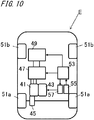
- FIG. 10 is a schematic structural diagram showing an embodiment of an electric vehicle.
- FIG. 10 shows an example of a hybrid electric vehicle (HEV) serving as an electric vehicle E.
- HEV hybrid electric vehicle
- reference numeral 41 denotes a driving motor
- reference numeral 43 denotes an engine
- reference numeral 45 denotes a transmission
- reference numeral 47 denotes an inverter
- reference numeral 49 denotes a power supply (battery)
- reference numerals 51a and 51b denote a front wheel and a rear wheel, respectively.
- the electric vehicle E has a function of transmitting an output of the motor 41, the engine 43 or both of them serving as the drive source to the pair of left and right front wheels 51a via the transmission 45.
- the power supply 49 is connected to the motor 41 via the inverter 47.
- the electric vehicle E shown in FIG. 10 is provided with a vehicle ECU 53 which performs comprehensive control of the entire electric vehicle E.
- Drive signals corresponding to the operation by a driver or the like from the electric vehicle E such as an ignition key 55, an accelerator pedal or a brake (not shown) are inputted to the vehicle ECU 53.
- the vehicle ECU 53 outputs instruction signals to the engine ECU 57, the power supply 49, and the inverter 47 serving as a load based on the drive signals.
- the engine ECU 57 controls a rotation speed of the engine 43 in response to the instruction signals to drive the electric vehicle E.
- the inverter D which uses the film capacitors A, B or the combination type capacitor C of the present embodiment as the capacitance member 33 is mounted on, for example, the electric vehicle E as shown in FIG. 10 , since the film capacitors A, B or the combination type capacitor C has an excellent self-recoverability and is reduced in the capacitance reduction, it is possible to maintain electrostatic capacitance for a long period of time, thereby reducing switching noise generated in the inverter 47 or the like for a long time.
- the inverter D of the present embodiment can be applied not only to the above-described hybrid electric vehicle (HEV) but also to various power conversion application products such as the electric vehicle (EV), a fuel cell vehicle, an electric bicycle, a generator, or a solar battery.
- the dielectric film having an average thickness of 2.5 ⁇ m was prepared using polyarylate (U-100, manufactured by UNITIKA).
- the dielectric film was formed into a sheet shape by dissolving polyarylate in toluene and coating it on a base material of a polyethylene terephthalate (PET) using a coater. After forming, the sheet was heated at 130°C to remove toluene and obtain the dielectric film.
- PET polyethylene terephthalate
- the obtained dielectric film was peeled from the base material and slit-processed to have a width of 130 mm, and then an Al (aluminum) metal film with a width of 97 mm was formed on one main surface of the dielectric film.
- the Al metal film was formed by a vacuum vapor deposition method with a metal mask and an oil mask at a predetermined position. The vacuum vapor deposition was performed twice.
- the thickness of the metal film was determined by a scanning electron microscope (SEM) observation of a cross-section processed by ion milling.
- the sheet resistance of the metal film was evaluated by a four-terminal resistance measurement mode using a multimeter.
- the film thickness of the first portion and the second portion not having the oil mask was 15 nm
- the sheet resistance thereof was 50 ⁇ /square
- the film thickness of the third portion having the oil mask was 8 nm
- the sheet resistance thereof was 100 ⁇ /square.
- a mesh pattern (see FIG. 4A ) was formed in a region to be the second portion of the metal film using a green laser marker.
- Example 4 a pattern in which the first portion and the second portion are directly adjacent to each other without the third portion was also produced.
- Laser irradiation conditions were output 4 W, frequency 140 kHz, and scan speed 4 m/s.
- the mesh pattern of the second portion was a pattern including small regions of 2 mm ⁇ 2 mm and a fuse portion of 0.4 mm width connecting the small regions.
- the metal film-attached film of 130 mm width was further slit-processed to prepare the metal film-attached film of 50 mm width having the 1.5 mm insulation margin portion (metal film non-formed portion with exposed dielectric film).
- the width direction was a first direction (x direction)
- a first portion located at one end thereof, a second portion adjacent to an insulation margin portion located at the other end, and a third portion located between the first portion and the second portion were disposed.
- a length W3 of the third portion in the first direction (x direction) was set such that the ratio (W3/W0) to the width W0 of the metal film-attached film (dielectric film) is 0.5, 0.3 and 0.25.
- W3/W0 0.5
- Example 2 a case where W3/W0 is 0.3
- Example 3 a case where W3/W0 is 0.25 is referred to as Example 3.
- the first portion located at one end in the first direction (x direction) and the second portion adjacent to the insulation margin portion located at the other end were disposed to be adjacent to each other at a center of the metal film-attached film.
- the width W1 of the first portion and the width W2 of the second portion were set to be equal.
- a column formed of polypropylene (PP) having an outer diameter of 5 mm and a length of 50 mm was used as a winding core.
- a pair of metal film-attached films having a width of 50 mm was overlapped so that the metal films faced each other with the dielectric film interposed therebetween and wound around the winding core to produce a wound body.
- the pair of metal film-attached films were wound in a state where they were offset from each other by 0.5 mm in the first direction (x direction) and the insulation margin portions were disposed on different sides in the first direction (x direction), respectively, to obtain the wound body (main body portion).
- the number of winding was 50 times.
- An alloy of zinc and tin was thermally sprayed on opposing end surfaces of the wound body (main body portion) in which the metal film was exposed, to form the metallikon electrodes which are the external electrodes to obtain the film capacitor.
- the electrostatic capacitance of the manufactured film capacitor was measured under conditions of 1 V AC and 1 kHz using an LCR meter.
- the electrostatic capacitance was 20 ⁇ F in all Examples 1-4.
- a heat generation state and a capacitance reduction rate of the film capacitor were evaluated as follows.
- a signal obtained by amplifying a sinusoidal wave of 10 kHz outputted by a function generator to a current of 100 A by a bipolar power supply was applied to the film capacitor at an initial temperature of 105°C.
- a surface temperature was saturated, a temperature in the central portion in the axial direction (x direction) was measured and compared with the initial temperature (105°C).
- the capacitance reduction rate after the application of the DC voltage was 15% in Example 4 not having the third portion, but it was 12% or less in Examples 1 to 3, and it was confirmed that the heat generation was suppressed by having the third portion.
Landscapes
- Engineering & Computer Science (AREA)
- Power Engineering (AREA)
- Microelectronics & Electronic Packaging (AREA)
- Manufacturing & Machinery (AREA)
- Fixed Capacitors And Capacitor Manufacturing Machines (AREA)
Abstract
Description
- The present disclosure relates to a film capacitor, a combination type capacitor, and an inverter and an electric vehicle using the same.
- The film capacitor has, for example, a dielectric film obtained by forming a polypropylene resin into a film, and a metal film formed on a surface of the dielectric film by vapor deposition. The metal film is used as an electrode. With such a configuration, the film capacitor has an advantage that even when short-circuiting occurs in an insulation defect portion of the dielectric film, the metal film around the defect portion evaporates and scatters due to a short circuit energy, and the insulation defect portion is insulated, so that dielectric breakdown of the film capacitor can be prevented (self-recovery property).
- In this manner, the film capacitor can prevent ignition and electric shock when an electric circuit is short-circuited. Focusing on this point, recently, the film capacitor has been applied to a power supply circuit such as LED (Light Emitting Diode) lighting and the like, and applications are expanding to motor drive of hybrid cars, an inverter system for solar power generation, and the like.
- In the film capacitor, when the self-recovery property functions as described above, the metal film around the insulation defect portion evaporates and scatters for insulation. As a result, an area of the electrode for generating electrostatic capacitance is reduced and a capacitance of the film capacitor is reduced. In order to suppress reduction in capacitance after self-recovery, a film capacitor in which a deposition electrode in the vicinity of an insulation margin portion is divided into a plurality of small regions and these regions are connected in parallel by fuses is disclosed (see, for example, Patent Literature 1). In the film capacitor having such a structure, when the self-recovery property functions, the fuse is blown and the region having the defect portion can be separated from the electric circuit.
- Patent Literature 1: Japanese Unexamined Patent Publication
JP-A 2009-164328 - A film capacitor of the present disclosure includes: a main body portion including a dielectric film and a metal film; and external electrodes, the external electrodes being disposed at a pair of main body ends which are both ends in a first direction of the main body portion, respectively. The metal film includes a first portion connected to an external electrode of the external electrodes which is disposed at one of the main body ends, a second portion disposed at the other main body end, and a third portion disposed between the first portion and the second portion in the first direction. A film thickness of the third portion is smaller than a film thickness of the second portion.
- A combination type capacitor of the present disclosure includes a plurality of film capacitors and at least one bus bar connecting all of the plurality of film capacitors, the plurality of film capacitors including the above-described film capacitor.
- An inverter of the present disclosure includes a bridge circuit including switching elements and a capacitance member connected to the bridge circuit, the capacitance member including the above-described film capacitor or the above-described combination type capacitor.
- An electric vehicle of the present disclosure includes a power supply, an inverter connected to the power supply, a motor connected to the inverter, and a wheel driven by the motor, the inverter including the above-described inverter.
-
-
FIG. 1 is a schematic cross-sectional view of a laminated type film capacitor; -
FIG. 2 is an exploded perspective view schematically showing a structure of a wound type film capacitor; -
FIG. 3A is a plan view of a surface showing a part of a dielectric film and a metal film; -
FIG. 3B is a transverse cross-sectional view showing a part of the dielectric film and the metal film; -
FIG. 4A is an enlarged plan view of a part (broken line portion) ofFIG. 3A ; -
FIG. 4B is an enlarged transverse cross-sectional view of a part (broken line portion) ofFIG. 3B ; -
FIG. 5 shows an arrangement in which a pair of metal film-attached films are overlapped, wherein an upper part is a plan view of one metal film-attached film and a lower part is a plan view of the other metal film-attached film; -
FIG. 6 is a transverse cross-sectional view showing a laminated structure of the dielectric film and the metal film; -
FIG. 7 is an enlarged view of a part (broken line portion) ofFIG. 5 , wherein an upper part is an enlarged plan view of a part of the upper part ofFIG. 5 and a lower part is an enlarged plan view of a part of the lower part ofFIG. 5 ; -
FIG. 8 is a perspective view schematically showing a structure of a combination type capacitor; -
FIG. 9 is a schematic structural diagram for explaining a structure of an embodiment of an inverter; and -
FIG. 10 is a schematic structural diagram showing an embodiment of an electric vehicle. - As shown in
FIGS. 1 and2 , the film capacitor includes a film capacitor main body portion 3 (hereinafter also referred to simply as a main body portion 3) in whichdielectric films metal films external electrodes main body portion 3 by metal spraying. - In the
main body portion 3 of a laminated type film capacitor A shown inFIG. 1 , a metal film-attachedfilm 5a provided with ametal film 2a on a first surface lac of adielectric film 1a, and a metal film-attachedfilm 5b provided with ametal film 2b on a first surface 1bc of adielectric film 1b are alternately laminated. Themetal film 2a is electrically connected to theexternal electrode 4a at onemain body end 3a of themain body portion 3. Themetal film 2b is electrically connected to theexternal electrode 4b at the othermain body end 3b of themain body portion 3. - In
FIG. 1 , a width direction of thedielectric films metal films dielectric films metal films external electrodes main body ends main body portion 3, respectively. - In the
main body portion 3 of a wound type film capacitor B shown inFIG. 2 , the metal film-attachedfilm 5a provided with themetal film 2a on the first surface lac of thedielectric film 1a, and the metal film-attachedfilm 5b provided with themetal film 2b on the first surface 1bc of thedielectric film 1b are laminated and then wound. Themetal film 2a is electrically connected to theexternal electrode 4a at the onemain body end 3a of themain body portion 3. Themetal film 2b is electrically connected to theexternal electrode 4b at the othermain body end 3b of themain body portion 3. - In
FIG. 2 , in order to facilitate understanding, thicknesses of thedielectric films metal films - In
FIG. 2 , the width direction of thedielectric films metal films dielectric films metal films external electrodes main body ends main body portion 3, respectively. In the film capacitor B, the x direction is the same as an axial direction of winding. - The
dielectric film 1a of the film capacitors A and B has the first surface lac and the second surface 1ad which are opposed to each other, and thedielectric film 1b thereof has the first surface 1bc and the second surface 1bd which are opposed to each other. The metal film-attachedfilm 5a is a film in which themetal film 2a is formed on the first surface lac of thedielectric film 1a, and has a so-calledinsulation margin portion 6a in which thedielectric film 1a is exposed on a part of the first surface 1ac. The metal film-attachedfilm 5b is a film in which themetal film 2b is formed on the first surface 1bc of thedielectric film 1b, and has a so-calledinsulation margin portion 6b in which thedielectric film 1b is exposed on a part of the first surface 1bc. As shown inFIGS. 1 and2 , these metal film-attachedfilms - In this manner, in the film capacitors A and B, the metal film-attached
film 5a including thedielectric film 1a and themetal film 2a and the metal film-attachedfilm 5b including thedielectric film 1b and themetal film 2b are overlapped and laminated or wound as shown inFIGS. 1 and2 . - The
metal films external electrodes main body ends main body portion 3. - In order to explain features of the present embodiment common to the metal film-attached
films FIG. 3A . Further, in a transverse cross-sectional view ofFIG. 3B , the thickness direction (z direction) of the film is enlarged in order to facilitate understanding. - In the present embodiment, as shown in
FIGS. 3A and 3B , themetal film 2 includes afirst portion 21, asecond portion 2m, and athird portion 2n. Thefirst portion 21 is located on a left main body end side and is connected to an external electrode 4 (not shown). Thesecond portion 2m is located in the vicinity of a right main body end, that is, in the vicinity of theinsulation margin portion 6, and is not directly connected to the external electrode 4 (not shown). Thethird portion 2n is located between thefirst portion 21 and thesecond portion 2m in the x direction. In themetal film 2, thefirst portion 21 and thesecond portion 2 m are disposed at both ends in the x direction, respectively, and thethird portion 2n is sandwiched between thefirst portion 21 and thesecond portion 2m. - The
first portion 21 and thethird portion 2n are continuous metal films. Since thefirst portion 21 is a continuous film and connected to theexternal electrode 4, an ESR is reduced. -
FIG. 3B is a transverse cross-sectional view ofFIG. 3A , andFIG. 4A is an enlarged plan view of a broken line portion ofFIG. 3A . As shown inFIGS. 3B and4A , thesecond portion 2m may comprise a plurality of small regions 2mi and afuse portion 8m connecting the small regions 2mi. The plurality of small regions 2mi are separated by intermittent mesh-like (lattice-like)grooves 7m. The adjacent small regions 2mi are electrically connected to each other by thefuse portion 8m. The small region 2mi and thefuse portion 8m can be formed by, for example, laser processing. A width of thegroove 7m may be, for example, 0.01 to 0.20 mm. - In this way, since the
second portion 2m has the small regions 2mi and the small regions 2mi are connected by thefuse portion 8m, it is possible to separate an insulation defect portion from an electric circuit by fusing thefuse portion 8m around the insulation defect portion by a short-circuit current at the time of self-recovery. Therefore, film capacitors A and B having an excellent self-recoverability can be obtained. In addition, there is an advantage that components evaporated by self-recovery tend to be evaporated to the outside through the mesh-like (lattice-like)grooves 7m. - It is sufficient that the
second portion 2m has the plurality of small regions 2mi and thefuse portion 8m connecting the small regions 2mi, and thegroove 7m may not be mesh-like (lattice-like). For example, thesecond portion 2m may have band-like (horizontal striped) small regions 2mi extending in the x direction, which are divided by thegrooves 7m extending in the x direction. -
FIGS. 5 to 7 show an arrangement in which the metal film-attachedfilms film 5a shown in the upper part ofFIG. 5 and the metal film-attachedfilm 5b shown in the lower part ofFIG. 5 are overlapped with each other slightly shifted in the width direction (x direction) as shown in the transverse cross-sectional view ofFIG. 6 . The upper part ofFIG. 7 is an enlarged view of the broken line portion of the upper part ofFIG. 5 , and the lower part ofFIG. 7 is an enlarged view of the broken line portion of the lower part ofFIG. 5 . The metal film-attachedfilms first portion 21a of themetal film 2a overlaps a second portion 2mb of themetal film 2b, and a second portion 2ma of themetal film 2a overlaps afirst portion 21b of themetal film 2b. - A third portion 2na of the
metal film 2a and a third portion 2nb of themetal film 2b are disposed to overlap each other. The third portion 2na of themetal film 2a may partially overlap the second portion 2mb or thefirst portion 21b of themetal film 2b. The third portion 2nb of themetal film 2b may partially overlap the second portion 2ma or thefirst portion 21a of themetal film 2a. - In the present embodiment, since the
third portion 2n is disposed between thefirst portion 21 and thesecond portion 2m, when the metal film-attachedfilms metal film 2a and the second portion 2mb of themetal film 2b do not overlap each other. Therefore, as shown inFIG. 6 , a fuse portion 8ma of the second portion 2ma and a fuse portion 8mb of the second portion 2mb do not overlap each other. In other words, since thefuse portions 8m do not concentrate in a central portion in the x direction of the film capacitors A and B, concentration of heat generation is suppressed, and it is possible to suppress dielectric breakdown at the central portion in the x direction of the film capacitors A and B. - As shown in
FIGS. 3B and4B , thefirst portion 21 and thethird portion 2n of themetal film 2 are continuous at a boundary between thefirst portion 21 and thethird portion 2n. Further, the small region 2mi adjacent to thethird portion 2n of themetal film 2 is continuous with thethird portion 2n at a boundary between thesecond portion 2m and thethird portion 2n.
Therefore, in the present embodiment, the grooves and the fuses are not concentratedly disposed in the vicinity of the boundary between thefirst portion 21 and thethird portion 2n and the boundary between thesecond portion 2m and thethird portion 2n. That is, since the fuses do not concentrate even in the vicinity of the boundary between thefirst portion 21 and thethird portion 2n and the boundary between thesecond portion 2m and thethird portion 2n, it is possible to suppress the concentration of heat generation in this region, thereby suppressing the dielectric breakdown. In addition, it is possible to suppress occurrence of wrinkles due to concentration of the grooves at a specific location during lamination or winding. - As described above, in the
second portion 2m having the small regions 2mi and thefuse portions 8m, when a self-recovery phenomenon occurs in the insulation defect portion, the short-circuit current flows in thefuse portion 8m around the insulation defect portion, and thefuse portion 8m generates heat and is fused, so that the insulation defect portion can be separated from the electric circuit. This is because a width of thefuse portion 8m is narrow and an electrical resistance is high. In the conventional film capacitor, there are portions where the fuse portions 8ma and 8mb overlap each other near the center in the x direction, that is, portions where thefuse portions 8m concentrate over a plurality of layers (winding layers), and when thefuse portions 8m generate heat and are fused in a part of the layers (winding layers), thefuse portions 8m in the other layers (winding layers) are also fused by the heat, and a capacitance has been greatly reduced. - On the other hand, in the present embodiment, the
third portion 2n is disposed between thefirst portion 21 and thesecond portion 2m. Thethird portion 2n does not have thefuse portion 8m but has a smaller film thickness than thesecond portion 2m. In general, the same metallic material is used for themetal film 2 regardless of portion. Therefore, a sheet resistance of themetal film 2 changes by adjusting the film thickness of themetal film 2. In other words, thethird portion 2n having a small film thickness of themetal film 2 can be the portion having a high sheet resistance. - Therefore, in the
third portion 2n, that is, in the portion where the film thickness is small of themetal film 2, themetal film 2 evaporates and scatters with a smaller amount of heat than the other portion (fuseportion 8m). Therefore, in thethird portion 2n, even when the self-recovery occurs, the heat generation is suppressed to a smaller level than when thefuse portion 8m is fused. Further, since themetal film 2 is continuous without being divided at thethird portion 2n, the generated heat easily diffuses in a plane of themetal film 2. Therefore, the diffusion of heat to themetal film 2 in the other layer (wound layer) is suppressed and an influence of evaporation/scattering of themetal film 2 does not reach the other layer (wound layer), and thus it is possible to reduce reduction in capacitance of the film capacitors A and B. - That is, by placing the
third portion 2n having a high electrical resistance (sheet resistance) between thefirst portion 21 and thesecond portion 2m, it is possible to suppress the concentration of heat generation due to concentration of thefuse portions 8m while maintaining the self-recoverability of the film capacitors A and B, and to reduce a possibility that thefuse portions 8m are blown at the same time over the plurality of layers (winding layers), thereby reducing reduction in capacitance at the time of self-recovery. - In this way, since the film thickness of the
third portion 2n located between thefirst portion 21 and thesecond portion 2m located at both ends in the x direction is small (has a high sheet resistance), in the present embodiment, it is possible to maintain the self-recoverability (withstand voltage) even in a region in which thethird portions 2n (2na and 2nb) of the film capacitors A and B overlap each other. In other words, since thethird portion 2n having a small film thickness is disposed at a portion (near the center in the width direction (x direction)) in which thefuse portion 8m does not exist when the metal film-attachedfilms - Even when the
second portion 2m is not divided into the plurality of small regions 2mi by thegroove 7m, that is, thesecond portion 2m is the continuous metal film, since thethird portion 2n having a high resistance is sandwiched between thefirst portion 21 and thesecond portion 2m, when the insulation defect occurs in the vicinity of the center in the x direction of the film capacitors A and B, the metal films 2na and 2nb of the insulation defect portion tend to evaporate and scatter. Further, since the thickness of thethird portion 2n is small, a gap is formed between the metal film-attachedfilms third portion 2n. Therefore, the evaporated and scattered metal components are likely to escape to the outside through the gap, resulting in the film capacitors A and B having a good self-recovery function. - As shown in
FIG. 3B , the length of thedielectric film 1 in the x direction is defined as W0, the length of the first portion in the x direction is defined as W1, the length of the second portion in the x direction is defined as W2, and the length of the third portion in the x direction is defined as W3. A sum (W1 + W3) of W1 and W3 is preferably larger than W2. Since (W1 + W3) is made larger than W2, even when the metal film-attachedfilms second portions 2m (2ma and 2mb) overlap each other is not formed, and thefuse portions 8m do not concentrate. - W2 is preferably larger than W1. By setting W2 to be larger than W1, the film capacitors A and B having an excellent self-recoverability can be obtained.
- The length of W3 may be 0.2 to 0.5 as a ratio of W3 to W0 (W3/W0). By setting W3/W0 equal to or more than 0.2, it is possible to dispose the
fuse portions 8m of thesecond portion 2m do not overlap each other in the vicinity of the center in the x direction, thereby obtaining a sufficient effect of preventing the heat generation. Further, by setting it to 0.5 or less, even when the self-recovery occurs at thethird portion 2n, it is possible to suppress reduction in capacitance of the film capacitors A and B. - As shown in
FIG. 3B andFIG. 6 , the metal films 2 (2a, 2b) may have a heavy edge structure in the vicinity (2f) of the connection portions with the external electrodes 4 (4a, 4b). Hereinafter, thevicinity 2f of the connecting portion of themetal film 2 to theexternal electrode 4 may also be referred to as aheavy edge portion 2f. The heavy edge structure is a structure in which the resistance of themetal film 2 in thevicinity 2f of the connection portion with theexternal electrode 4 is reduced with respect to an effective region in which themetal films - The film thickness of the
metal film 2 is preferably, for example, 20 nm or less, particularly 5 to 15 nm in thefirst portion 21 and thesecond portion 2m. By setting thefirst portion 21 and thesecond portion 2m of themetal film 2 to such a film thickness, an area resistance (the sheet resistance) is 18 to 50 Ω/square and the self-recoverability can be obtained. Further, the film thickness of themetal film 2 in thevicinity 2f of the connection portion with theexternal electrode 4 is preferably set to be 2 to 4 times thefirst portion 21 and thesecond portion 2m, that is, in a range of 10 to 80 nm. The thickness of thefirst portion 21 may be larger than the thickness of thesecond portion 2m. By setting the film thickness of thefirst portion 21 connected to theexternal electrode 4 to be larger than the film thickness of thesecond portion 2m, the equivalent series resistance (ESR) of the film capacitors A and B can be reduced. - The thickness of the
metal film 2 at thethird portion 2n may be, for example, 0.2 to 0.6 times the film thickness of thefirst portion 21 and thesecond portion 2m. By setting the film thickness to such a thickness, the sheet resistance can be increased more than that of thesecond portion 2m, and even when the insulation defect occurs in thethird portion 2n, the self-recoverability can be sufficiently obtained with a small amount of heat. The film thickness of themetal film 2 may be confirmed, for example, by using a scanning electron microscope (SEM) or the like for a cross-section of the metal film-attachedfilm 5 processed by ion milling. - Examples of insulating resin materials used for the
dielectric film 1 include polypropylene (PP), polyethylene terephthalate (PET), polyphenylene sulfide (PPS), polyethylene naphthalate (PEN), polyarylate (PAR), polyphenylene ether (PPE), polyetherimide (PEI) and cycloolefin polymer (COP). In particular, the polyarylate (PAR) has a high breakdown voltage. - Such film capacitors A and B may be produced, for example, as follows. First, the
dielectric film 1 is prepared. Thedielectric film 1 is obtained, for example, by forming a resin solution in which an insulating resin is dissolved in a solvent, into a sheet shape on a surface of a base material formed of polyethylene terephthalate (PET), and by drying it to volatilize the solvent. A forming method may be appropriately selected from well-known film forming methods such as a doctor blade method, a die coater method and a knife coater method. As the solvent used for forming, for example, methanol, isopropanol, n-butanol, ethylene glycol, ethylene glycol monopropyl ether, methyl ethyl ketone, methyl isobutyl ketone, xylene, propylene glycol monomethyl ether, propylene glycol monomethyl ether acetate, dimethylacetamide, cyclohexane, or an organic solvent containing a mixture of two or more selected from them is preferably used. Further, a resin film produced by a melt extrusion method may be stretched. - The thickness of the
dielectric film 1 may be, for example, 5 µm or less, however, it is particularly preferable to use thedielectric film 1 having a thickness of 0.5 to 4 µm. - The
dielectric film 1 may be composed of only the insulating resin described above, but may contain other materials. Examples of constituent elements other than the resin contained in thedielectric film 1 include the above-described organic solvents and inorganic fillers. As the inorganic filler, for example, inorganic oxides such as alumina, titanium oxide, silicon dioxide, inorganic nitrides such as silicon nitride, glass or the like can be used. Particularly when a material having a high relative permittivity, such as a complex oxide having a perovskite structure, is used as the inorganic filler, the relative permittivity of the entiredielectric film 1 can be improved and the film capacitor can be downsized. In order to improve compatibility between the inorganic filler and the resin, surface treatment such as silane coupling treatment or titanate coupling treatment may be performed on the inorganic filler. - When such an inorganic filler is used for the
dielectric film 1, by producing the composite film containing less than 50 mass% of the inorganic filler and 50 mass% or more of the resin, it is possible to obtain effects such as improvement of the relative permittivity by the inorganic filler while maintaining flexibility of the resin. Further, a size (an average particle diameter) of the inorganic filler is preferably 4 to 1000 nm. - One of ends in the width direction (x direction) of one surface of the produced
dielectric film 1 is masked. By vapor depositing a metal component such as aluminum (Al) on an unmasked portion of the one surface of thedielectric film 1 to form themetal film 2, the metal film-attachedfilm 5 having theinsulation margin portion 6 is obtained. - When forming the
metal film 2 having thefirst portion 21, thesecond portion 2m and thethird portion 2n, for example, when forming themetal film 2 on thedielectric film 1, it may be formed by the following procedure. A region in which thethird portion 2n of themetal film 2 is to be formed on the one surface of thedielectric film 1 is applied with oil, to be masked (oil mask). First vapor deposition is performed on the oil-maskeddielectric film 1 using a resistance heating vacuum vapor deposition apparatus. At this time, a vapor deposition film to be thefirst portion 21 and thesecond portion 2m is formed, and the oil mask applied to a portion to be thethird portion 2n is volatilized. Thereafter, a second vapor deposition is further performed, so that the vapor deposition film is also formed in a region where the oil mask is volatilized. The obtained metal film-attachedfilm 5 has a vapor deposition film to be thesecond portion 2m on one side (on theinsulation margin portion 6 side) of the ends in the width direction (x direction), and has thefirst portion 21 on the other side, with thethird portion 2n having a small film thickness of themetal film 2 interposed therebetween. - When forming the heavy edge structure, a portion other than a portion forming the heavy edge of the above-described metal film-attached
film 5 is masked, and for example, zinc (Zn) is further formed by vapor deposition (third vapor deposition) on a mask-free portion of the above-described vapor deposited metal components (first and second vapor deposition films). The film thickness of the vapor deposition film for the third vapor deposition to form theheavy edge portion 2f is set to 1 to 3 times the film thickness of the above-described vapor deposited metal components (first and second vapor deposition films). Thus, the film thickness of theheavy edge portion 2f is 2 to 4 times the film thickness of the otherfirst portion 21 and thesecond portion 2m (the sum of the film thicknesses of the vapor deposition films formed by the first vapor deposition and the second vapor deposition). - Next, the
groove 7m is formed in a portion to be thesecond portion 2m of themetal film 2. A laser marker or a laser trimmer capable of blowing off a metal evaporated film is used for forming thegroove 7m. One of green laser, YAG laser and CO2 laser may be used as a laser. - As shown in
FIGS. 1 and2 , the metal film-attached films 5 (5a, 5b) having the metal film 2 (2a, 2b) on one surface thereof are overlapped or wound with each other as a set slightly shifted in the width direction (x direction) to obtain themain body portion 3. - The film capacitors A and B are obtained by forming metallikon electrodes as the
external electrodes 4 on both end surfaces in the x direction of the obtainedmain body 3. For example, metal spraying, sputtering, plating or the like may be used for forming theexternal electrodes 4. - Then, an outer surface of the
main body portion 3 on which theexternal electrode 4 is formed can be covered with an exterior member (not shown) as needed. - Examples of a material of the
metal film 2 include a metal such as aluminum (Al) or zinc (Zn) and an alloy. - Further, as a material of the metallikon electrode, at least one metallic material selected from zinc, aluminum, copper and solder is suitable.
-
FIG. 8 is a perspective view schematically showing a structure of an embodiment of a combination type capacitor. InFIG. 8 , in order to facilitate understanding of the structure, description of a case and a resin for molding is omitted. A combination type capacitor C of the present embodiment is configured such that a plurality of wound type film capacitors B are connected in parallel via a pair ofbus bars connection terminal portions terminal portions external electrodes - When the above-described film capacitor B is applied to the combination type capacitor C, it is possible to obtain the combination type capacitor C which has an excellent self-recoverability and is reduced in capacitance reduction. Note that the laminated type film capacitor A may be used instead of the wound type film capacitor B.
- The combination type capacitor C can be obtained by attaching the bus bars 21 and 23 to the
external electrodes main body portion 3, respectively, via a bonding material in a state where a plurality of (four in the present embodiment) film capacitors B are juxtaposed. - The film capacitor A, B and the combination type capacitor C may also be formed into a resin-molded (case-molded) capacitor by housing the film capacitor A, B or the combination type capacitor C in a case and then filling a space in the case with the resin.
- The combination type capacitor C shown in
FIG. 8 is the capacitor in which the film capacitors B are juxtaposed in a direction of a long diameter of a cross-section perpendicular to a winding axis thereof, however, as another structure, the film capacitors B may be stacked in a direction of a short diameter of the cross-section perpendicular to the winding axis thereof. -
FIG. 9 is a schematic structural diagram for explaining a structure of an embodiment of an inverter.FIG. 9 shows an example of an inverter D which creates an alternating current from a direct current. As shown inFIG. 9 , the inverter D of the present embodiment includes a bridge circuit 31 including switching elements (for example, IGBT (Insulated Gate Bipolar Transistor)) and diodes, and acapacitance member 33 disposed between input terminals of the bridge circuit 31 for voltage stabilization. Here, the film capacitor A or B, or the combination type capacitor C described above is used as thecapacitance member 33. - The inverter D is connected to a
booster circuit 35 for boosting a voltage of a DC power supply. On the other hand, the bridge circuit 31 is connected to a motor generator (motor M) which is a drive source. -
FIG. 10 is a schematic structural diagram showing an embodiment of an electric vehicle.FIG. 10 shows an example of a hybrid electric vehicle (HEV) serving as an electric vehicle E. - In
FIG. 10 ,reference numeral 41 denotes a driving motor,reference numeral 43 denotes an engine,reference numeral 45 denotes a transmission,reference numeral 47 denotes an inverter, reference numeral 49 denotes a power supply (battery), andreference numerals - The electric vehicle E has a function of transmitting an output of the
motor 41, theengine 43 or both of them serving as the drive source to the pair of left and rightfront wheels 51a via thetransmission 45. The power supply 49 is connected to themotor 41 via theinverter 47. - The electric vehicle E shown in
FIG. 10 is provided with avehicle ECU 53 which performs comprehensive control of the entire electric vehicle E. Drive signals corresponding to the operation by a driver or the like from the electric vehicle E such as anignition key 55, an accelerator pedal or a brake (not shown) are inputted to thevehicle ECU 53. Thevehicle ECU 53 outputs instruction signals to theengine ECU 57, the power supply 49, and theinverter 47 serving as a load based on the drive signals. Theengine ECU 57 controls a rotation speed of theengine 43 in response to the instruction signals to drive the electric vehicle E. - When the inverter D which uses the film capacitors A, B or the combination type capacitor C of the present embodiment as the
capacitance member 33 is mounted on, for example, the electric vehicle E as shown inFIG. 10 , since the film capacitors A, B or the combination type capacitor C has an excellent self-recoverability and is reduced in the capacitance reduction, it is possible to maintain electrostatic capacitance for a long period of time, thereby reducing switching noise generated in theinverter 47 or the like for a long time. - The inverter D of the present embodiment can be applied not only to the above-described hybrid electric vehicle (HEV) but also to various power conversion application products such as the electric vehicle (EV), a fuel cell vehicle, an electric bicycle, a generator, or a solar battery.
- The dielectric film having an average thickness of 2.5 µm was prepared using polyarylate (U-100, manufactured by UNITIKA). The dielectric film was formed into a sheet shape by dissolving polyarylate in toluene and coating it on a base material of a polyethylene terephthalate (PET) using a coater. After forming, the sheet was heated at 130°C to remove toluene and obtain the dielectric film.
- The obtained dielectric film was peeled from the base material and slit-processed to have a width of 130 mm, and then an Al (aluminum) metal film with a width of 97 mm was formed on one main surface of the dielectric film. The Al metal film was formed by a vacuum vapor deposition method with a metal mask and an oil mask at a predetermined position. The vacuum vapor deposition was performed twice. The thickness of the metal film was determined by a scanning electron microscope (SEM) observation of a cross-section processed by ion milling. The sheet resistance of the metal film was evaluated by a four-terminal resistance measurement mode using a multimeter. As a result, the film thickness of the first portion and the second portion not having the oil mask was 15 nm, the sheet resistance thereof was 50 Ω/square, the film thickness of the third portion having the oil mask was 8 nm, and the sheet resistance thereof was 100 Ω/square.
- A mesh pattern (see
FIG. 4A ) was formed in a region to be the second portion of the metal film using a green laser marker. As Example 4, a pattern in which the first portion and the second portion are directly adjacent to each other without the third portion was also produced. - Laser irradiation conditions were output 4 W, frequency 140 kHz, and scan speed 4 m/s. The mesh pattern of the second portion was a pattern including small regions of 2 mm × 2 mm and a fuse portion of 0.4 mm width connecting the small regions.
- The metal film-attached film of 130 mm width was further slit-processed to prepare the metal film-attached film of 50 mm width having the 1.5 mm insulation margin portion (metal film non-formed portion with exposed dielectric film). In the metal film-attached film of Example, as the width direction was a first direction (x direction), a first portion located at one end thereof, a second portion adjacent to an insulation margin portion located at the other end, and a third portion located between the first portion and the second portion were disposed. A length W3 of the third portion in the first direction (x direction) was set such that the ratio (W3/W0) to the width W0 of the metal film-attached film (dielectric film) is 0.5, 0.3 and 0.25. Hereinafter, a case where W3/W0 is 0.5 is referred to as Example 1, a case where W3/W0 is 0.3 is referred to as Example 2, and a case where W3/W0 is 0.25 is referred to as Example 3.
- In the metal film-attached film of Example 4, the first portion located at one end in the first direction (x direction) and the second portion adjacent to the insulation margin portion located at the other end were disposed to be adjacent to each other at a center of the metal film-attached film.
- In Examples 1-4, the width W1 of the first portion and the width W2 of the second portion were set to be equal.
- A column formed of polypropylene (PP) having an outer diameter of 5 mm and a length of 50 mm was used as a winding core. A pair of metal film-attached films having a width of 50 mm was overlapped so that the metal films faced each other with the dielectric film interposed therebetween and wound around the winding core to produce a wound body. Note that the pair of metal film-attached films were wound in a state where they were offset from each other by 0.5 mm in the first direction (x direction) and the insulation margin portions were disposed on different sides in the first direction (x direction), respectively, to obtain the wound body (main body portion). The number of winding was 50 times.
- An alloy of zinc and tin was thermally sprayed on opposing end surfaces of the wound body (main body portion) in which the metal film was exposed, to form the metallikon electrodes which are the external electrodes to obtain the film capacitor.
- The electrostatic capacitance of the manufactured film capacitor was measured under conditions of 1 V AC and 1 kHz using an LCR meter. The electrostatic capacitance was 20 µF in all Examples 1-4.
- A heat generation state and a capacitance reduction rate of the film capacitor were evaluated as follows. For the heat generation state, a signal obtained by amplifying a sinusoidal wave of 10 kHz outputted by a function generator to a current of 100 A by a bipolar power supply was applied to the film capacitor at an initial temperature of 105°C. After about 1 hour elapsed from the application of the signal, and a surface temperature was saturated, a temperature in the central portion in the axial direction (x direction) was measured and compared with the initial temperature (105°C). As for the capacitance reduction rate, after a DC voltage of 1200 V was applied to the film capacitor at room temperature for 120 seconds using an insulation resistance meter, the electrostatic capacitance was measured under conditions of
AC 1V and 1 kHz using an LCR meter and compared with the initial electrostatic capacitance (20 µF). Results are shown in Table 1.[Table 1] W3/W0 Temperature rise Capacitance reduction rate Example 1 0.5 8° C 12% Example 2 0.3 10° C 5% Example 3 0.25 12°C 8% Example 4 - 15°C 15% - Temperature rise from the initial temperature due to the application of the electric current was 15°C in Example 4 not having the third portion, but it was 12°C or less in Examples 1 to 3, and it was confirmed that the heat generation was suppressed by having the third portion. This is probably because the concentration of heat generation was suppressed without overlapping and concentrating the fuse portions by having the third portion in Examples 1 to 3.
- The capacitance reduction rate after the application of the DC voltage was 15% in Example 4 not having the third portion, but it was 12% or less in Examples 1 to 3, and it was confirmed that the heat generation was suppressed by having the third portion.
-
- A, B:
- Film capacitor
- C:
- Combination type capacitor
- D:
- Inverter
- E:
- Electric vehicle
- 1, 1a, 1b:
- Dielectric film
- 2, 2a, 2b:
- Metal film
- 21, 21a, 21b:
- First portion of metal film
- 2m, 2ma, 2mb:
- Second portion of metal film
- 2n, 2na, 2nb:
- Third portion of metal film
- 3:
- Main body portion
- 4, 4a, 4b:
- External electrode
- 5, 5a, 5b:
- Metal film-attached film
- 7m:
- Groove
- 8m:
- Fuse portion
- 21, 23:
- Bus bar
- 31:
- Bridge circuit
- 33:
- Capacitance member
- 35:
- Booster circuit
- 41:
- Motor
- 43:
- Engine
- 45:
- Transmission
- 47:
- Inverter
- 49:
- Power supply
- 51a:
- Front wheel
- 51b:
- Rear wheel
- 53:
- Vehicle ECU
- 55:
- Ignition key
- 57:
- Engine ECU
Claims (8)
- A film capacitor, comprising:a main body portion comprising a dielectric film and a metal film; andexternal electrodes,the external electrodes being disposed at a pair of main body ends which are both ends in a first direction of the main body portion, respectively,the metal film comprising a first portion, connected to an external electrode of the external electrodes, which is disposed at one of the main body ends, a second portion disposed at the other main body end, and a third portion disposed between the first portion and the second portion in the first direction,a film thickness of the third portion being smaller than a film thickness of the second portion.
- The film capacitor according to claim 1, wherein the metal film comprises a pair of metal films opposed to each other with the dielectric film interposed therebetween, and the pair of metal films are disposed so that at least a part of the third portion of one of the metal films overlaps a part of the third portion of the other metal film.
- The film capacitor according to claim 1 or 2, wherein the second portion comprises a plurality of small regions which are separated by intermittent mesh-like grooves, and fuse portions connecting the small regions.
- The film capacitor according to any one of claims 1 to 3, wherein a ratio of a W3 to a W0 (W3/W0) is 0.2 to 0.5, in which the W0 denotes a length in the first direction of the dielectric film, and the W3 denotes a length in the first direction of the third portion.
- A combination type capacitor, comprising:a plurality of film capacitors; andat least one bus bar connecting all of the plurality of film capacitors,the plurality of film capacitors comprising the film capacitor according to any one of claims 1 to 4.
- An inverter, comprising:a bridge circuit comprising switching elements and a capacitance member connected to the bridge circuit,the capacitance member comprising the film capacitor according to any one of claims 1 to 4.
- An inverter, comprising:a bridge circuit comprising switching elements and a capacitance member connected to the bridge circuit,the capacitance member comprising the combination type capacitor according to claim 5.
- An electric vehicle, comprising:a power supply;an inverter connected to the power supply;a motor connected to the inverter; anda wheel driven by the motor,the inverter comprising the inverter according to claim 6 or 7.
Applications Claiming Priority (2)
| Application Number | Priority Date | Filing Date | Title |
|---|---|---|---|
| JP2016089438 | 2016-04-27 | ||
| PCT/JP2017/016583 WO2017188327A1 (en) | 2016-04-27 | 2017-04-26 | Film capacitor, connected-type capacitor, inverter using same, and electric vehicle |
Publications (3)
| Publication Number | Publication Date |
|---|---|
| EP3435390A1 true EP3435390A1 (en) | 2019-01-30 |
| EP3435390A4 EP3435390A4 (en) | 2019-05-01 |
| EP3435390B1 EP3435390B1 (en) | 2020-05-13 |
Family
ID=60160874
Family Applications (1)
| Application Number | Title | Priority Date | Filing Date |
|---|---|---|---|
| EP17789609.9A Active EP3435390B1 (en) | 2016-04-27 | 2017-04-26 | Film capacitor, connected-type capacitor, inverter using same, and electric vehicle |
Country Status (5)
| Country | Link |
|---|---|
| US (1) | US10650965B2 (en) |
| EP (1) | EP3435390B1 (en) |
| JP (1) | JP6799588B2 (en) |
| CN (1) | CN109074955B (en) |
| WO (1) | WO2017188327A1 (en) |
Families Citing this family (5)
| Publication number | Priority date | Publication date | Assignee | Title |
|---|---|---|---|---|
| EP3712914B1 (en) * | 2017-11-15 | 2025-12-03 | Murata Manufacturing Co., Ltd. | Film capacitor |
| JP7466650B2 (en) * | 2020-07-31 | 2024-04-12 | 京セラ株式会社 | Film capacitor, coupled capacitor, inverter and electric vehicle |
| CN112277347B (en) * | 2020-09-24 | 2022-05-27 | 铜陵市超越电子有限公司 | Preparation device and processing method of anti-oxidation metallized film |
| CN113948314B (en) * | 2021-10-28 | 2023-02-24 | 厦门法拉电子股份有限公司 | Thin film capacitor |
| US20250385044A1 (en) * | 2024-06-12 | 2025-12-18 | BorgWarner US Technologies LLC | Systems for capacitor for inverter for electric vehicle |
Family Cites Families (24)
| Publication number | Priority date | Publication date | Assignee | Title |
|---|---|---|---|---|
| FR2225821A1 (en) * | 1973-04-13 | 1974-11-08 | Radiotechnique Compelec | Electric capacitors with metallised dielectric foil - longer life obtd. by thickening metal along border or leakage path |
| JPS596518A (en) * | 1982-07-02 | 1984-01-13 | 松下電器産業株式会社 | Wire wound condenser |
| JP3392525B2 (en) * | 1994-07-27 | 2003-03-31 | ニチコン株式会社 | Metallized film capacitors |
| IT236732Y1 (en) * | 1995-03-15 | 2000-08-17 | Icar Spa | METALLIC DIELECTRIC FILM AND RELATED CAPACITOR |
| JP2000100646A (en) * | 1998-09-25 | 2000-04-07 | Nissin Electric Co Ltd | Capacitor element |
| JP3914854B2 (en) * | 2002-10-10 | 2007-05-16 | 松下電器産業株式会社 | Metalized film capacitor, inverter smoothing capacitor and automotive capacitor using the same |
| US6984860B2 (en) * | 2002-11-27 | 2006-01-10 | Semiconductor Components Industries, L.L.C. | Semiconductor device with high frequency parallel plate trench capacitor structure |
| US7319599B2 (en) * | 2003-10-01 | 2008-01-15 | Matsushita Electric Industrial Co., Ltd. | Module incorporating a capacitor, method for manufacturing the same, and capacitor used therefor |
| EP1868216B1 (en) * | 2005-04-08 | 2014-01-01 | Panasonic Corporation | Metalized film capacitor and inverter smoothing capacitor for automobile |
| JP2008277562A (en) * | 2007-04-27 | 2008-11-13 | Daikin Ind Ltd | Capacitor unit |
| US7933111B2 (en) * | 2007-05-08 | 2011-04-26 | Nuinteck Co., Ltd | Metallized plastic film and film capacitor |
| JP4915947B2 (en) * | 2007-08-17 | 2012-04-11 | ニチコン株式会社 | Metallized film capacitors |
| JP5012515B2 (en) | 2008-01-07 | 2012-08-29 | パナソニック株式会社 | Metallized film capacitors |
| US20090225491A1 (en) * | 2008-03-04 | 2009-09-10 | Hui-Chuan Yao | Metallized film capacitor |
| US8451579B2 (en) * | 2008-07-08 | 2013-05-28 | Panasonic Corporation | Metalized film capacitor |
| KR101629851B1 (en) * | 2009-02-05 | 2016-06-14 | 니치콘 가부시키가이샤 | Metalized film capacitor |
| JP5344340B2 (en) * | 2009-02-27 | 2013-11-20 | 株式会社指月電機製作所 | Metallized film capacitors |
| CN102598170B (en) * | 2009-11-04 | 2014-07-30 | 松下电器产业株式会社 | Metallized film capacitor and case molded capacitor using same |
| CN201789431U (en) | 2010-08-04 | 2011-04-06 | 苏州西典机电有限公司 | General inverter module |
| US9266441B2 (en) * | 2011-01-19 | 2016-02-23 | Technova Inc. | Contactless power transfer system |
| CN103597561B (en) * | 2011-05-30 | 2016-11-23 | 松下知识产权经营株式会社 | Metallized Film Capacitors |
| JP5927481B2 (en) * | 2011-07-07 | 2016-06-01 | パナソニックIpマネジメント株式会社 | Metallized film capacitors |
| WO2015133473A1 (en) * | 2014-03-03 | 2015-09-11 | 京セラ株式会社 | Film capacitor, connected capacitor, inverter and electric vehicle |
| US9570239B2 (en) * | 2014-09-02 | 2017-02-14 | Samhwa Capacitor Co., Ltd. | Electrode forming film and film capacitor using the same |
-
2017
- 2017-04-26 US US16/095,578 patent/US10650965B2/en active Active
- 2017-04-26 WO PCT/JP2017/016583 patent/WO2017188327A1/en not_active Ceased
- 2017-04-26 CN CN201780024004.5A patent/CN109074955B/en active Active
- 2017-04-26 EP EP17789609.9A patent/EP3435390B1/en active Active
- 2017-04-26 JP JP2018514672A patent/JP6799588B2/en active Active
Also Published As
| Publication number | Publication date |
|---|---|
| JPWO2017188327A1 (en) | 2019-02-14 |
| US10650965B2 (en) | 2020-05-12 |
| EP3435390A4 (en) | 2019-05-01 |
| WO2017188327A1 (en) | 2017-11-02 |
| EP3435390B1 (en) | 2020-05-13 |
| JP6799588B2 (en) | 2020-12-16 |
| CN109074955B (en) | 2021-01-22 |
| US20190115152A1 (en) | 2019-04-18 |
| CN109074955A (en) | 2018-12-21 |
Similar Documents
| Publication | Publication Date | Title |
|---|---|---|
| EP3413323B1 (en) | Film capacitor, connected capacitor, and inverter and electric vehicle using same | |
| EP3435390B1 (en) | Film capacitor, connected-type capacitor, inverter using same, and electric vehicle | |
| CN111213217B (en) | Film capacitors, junction capacitors, inverters using the same, and electric vehicles | |
| JP6574922B1 (en) | Film capacitors, coupled capacitors, inverters and electric vehicles | |
| JP7011053B2 (en) | Film capacitors, articulated capacitors, inverters and electric vehicles using them | |
| JP6744486B2 (en) | Film capacitor, concatenated capacitor, and inverter and electric vehicle using the same | |
| JP6687373B2 (en) | Film capacitor, concatenated capacitor, and inverter and electric vehicle using the same | |
| JP6737818B2 (en) | Film capacitors, concatenated capacitors, inverters, and electric vehicles | |
| WO2018101260A1 (en) | Film capacitor, inverter and electric vehicle | |
| CN114041263B (en) | Laminated capacitor, connection-type capacitor, inverter, and electric vehicle |
Legal Events
| Date | Code | Title | Description |
|---|---|---|---|
| STAA | Information on the status of an ep patent application or granted ep patent |
Free format text: STATUS: THE INTERNATIONAL PUBLICATION HAS BEEN MADE |
|
| PUAI | Public reference made under article 153(3) epc to a published international application that has entered the european phase |
Free format text: ORIGINAL CODE: 0009012 |
|
| STAA | Information on the status of an ep patent application or granted ep patent |
Free format text: STATUS: REQUEST FOR EXAMINATION WAS MADE |
|
| 17P | Request for examination filed |
Effective date: 20181023 |
|
| AK | Designated contracting states |
Kind code of ref document: A1 Designated state(s): AL AT BE BG CH CY CZ DE DK EE ES FI FR GB GR HR HU IE IS IT LI LT LU LV MC MK MT NL NO PL PT RO RS SE SI SK SM TR |
|
| AX | Request for extension of the european patent |
Extension state: BA ME |
|
| A4 | Supplementary search report drawn up and despatched |
Effective date: 20190403 |
|
| RIC1 | Information provided on ipc code assigned before grant |
Ipc: H02M 7/48 20070101ALI20190328BHEP Ipc: H01G 4/015 20060101AFI20190328BHEP Ipc: H01G 4/38 20060101ALI20190328BHEP Ipc: H01G 4/32 20060101ALI20190328BHEP Ipc: H01G 2/04 20060101ALI20190328BHEP Ipc: H01G 4/012 20060101ALI20190328BHEP Ipc: H01G 4/18 20060101ALI20190328BHEP |
|
| DAV | Request for validation of the european patent (deleted) | ||
| DAX | Request for extension of the european patent (deleted) | ||
| GRAP | Despatch of communication of intention to grant a patent |
Free format text: ORIGINAL CODE: EPIDOSNIGR1 |
|
| STAA | Information on the status of an ep patent application or granted ep patent |
Free format text: STATUS: GRANT OF PATENT IS INTENDED |
|
| RIC1 | Information provided on ipc code assigned before grant |
Ipc: H01G 4/012 20060101ALI20191206BHEP Ipc: H02M 7/48 20070101ALI20191206BHEP Ipc: H01G 4/015 20060101AFI20191206BHEP Ipc: H01G 4/32 20060101ALI20191206BHEP Ipc: H01G 2/04 20060101ALI20191206BHEP Ipc: H01G 4/18 20060101ALI20191206BHEP Ipc: H01G 4/38 20060101ALI20191206BHEP |
|
| INTG | Intention to grant announced |
Effective date: 20200107 |
|
| GRAS | Grant fee paid |
Free format text: ORIGINAL CODE: EPIDOSNIGR3 |
|
| GRAA | (expected) grant |
Free format text: ORIGINAL CODE: 0009210 |
|
| STAA | Information on the status of an ep patent application or granted ep patent |
Free format text: STATUS: THE PATENT HAS BEEN GRANTED |
|
| AK | Designated contracting states |
Kind code of ref document: B1 Designated state(s): AL AT BE BG CH CY CZ DE DK EE ES FI FR GB GR HR HU IE IS IT LI LT LU LV MC MK MT NL NO PL PT RO RS SE SI SK SM TR |
|
| REG | Reference to a national code |
Ref country code: GB Ref legal event code: FG4D |
|
| REG | Reference to a national code |
Ref country code: CH Ref legal event code: EP |
|
| REG | Reference to a national code |
Ref country code: DE Ref legal event code: R096 Ref document number: 602017016803 Country of ref document: DE |
|
| REG | Reference to a national code |
Ref country code: AT Ref legal event code: REF Ref document number: 1271309 Country of ref document: AT Kind code of ref document: T Effective date: 20200615 |
|
| REG | Reference to a national code |
Ref country code: LT Ref legal event code: MG4D |
|
| REG | Reference to a national code |
Ref country code: NL Ref legal event code: MP Effective date: 20200513 |
|
| PG25 | Lapsed in a contracting state [announced via postgrant information from national office to epo] |
Ref country code: IS Free format text: LAPSE BECAUSE OF FAILURE TO SUBMIT A TRANSLATION OF THE DESCRIPTION OR TO PAY THE FEE WITHIN THE PRESCRIBED TIME-LIMIT Effective date: 20200913 Ref country code: PT Free format text: LAPSE BECAUSE OF FAILURE TO SUBMIT A TRANSLATION OF THE DESCRIPTION OR TO PAY THE FEE WITHIN THE PRESCRIBED TIME-LIMIT Effective date: 20200914 Ref country code: FI Free format text: LAPSE BECAUSE OF FAILURE TO SUBMIT A TRANSLATION OF THE DESCRIPTION OR TO PAY THE FEE WITHIN THE PRESCRIBED TIME-LIMIT Effective date: 20200513 Ref country code: NO Free format text: LAPSE BECAUSE OF FAILURE TO SUBMIT A TRANSLATION OF THE DESCRIPTION OR TO PAY THE FEE WITHIN THE PRESCRIBED TIME-LIMIT Effective date: 20200813 Ref country code: GR Free format text: LAPSE BECAUSE OF FAILURE TO SUBMIT A TRANSLATION OF THE DESCRIPTION OR TO PAY THE FEE WITHIN THE PRESCRIBED TIME-LIMIT Effective date: 20200814 Ref country code: SE Free format text: LAPSE BECAUSE OF FAILURE TO SUBMIT A TRANSLATION OF THE DESCRIPTION OR TO PAY THE FEE WITHIN THE PRESCRIBED TIME-LIMIT Effective date: 20200513 Ref country code: LT Free format text: LAPSE BECAUSE OF FAILURE TO SUBMIT A TRANSLATION OF THE DESCRIPTION OR TO PAY THE FEE WITHIN THE PRESCRIBED TIME-LIMIT Effective date: 20200513 |
|
| PG25 | Lapsed in a contracting state [announced via postgrant information from national office to epo] |
Ref country code: BG Free format text: LAPSE BECAUSE OF FAILURE TO SUBMIT A TRANSLATION OF THE DESCRIPTION OR TO PAY THE FEE WITHIN THE PRESCRIBED TIME-LIMIT Effective date: 20200813 Ref country code: HR Free format text: LAPSE BECAUSE OF FAILURE TO SUBMIT A TRANSLATION OF THE DESCRIPTION OR TO PAY THE FEE WITHIN THE PRESCRIBED TIME-LIMIT Effective date: 20200513 Ref country code: LV Free format text: LAPSE BECAUSE OF FAILURE TO SUBMIT A TRANSLATION OF THE DESCRIPTION OR TO PAY THE FEE WITHIN THE PRESCRIBED TIME-LIMIT Effective date: 20200513 Ref country code: RS Free format text: LAPSE BECAUSE OF FAILURE TO SUBMIT A TRANSLATION OF THE DESCRIPTION OR TO PAY THE FEE WITHIN THE PRESCRIBED TIME-LIMIT Effective date: 20200513 |
|
| REG | Reference to a national code |
Ref country code: AT Ref legal event code: MK05 Ref document number: 1271309 Country of ref document: AT Kind code of ref document: T Effective date: 20200513 |
|
| PG25 | Lapsed in a contracting state [announced via postgrant information from national office to epo] |
Ref country code: AL Free format text: LAPSE BECAUSE OF FAILURE TO SUBMIT A TRANSLATION OF THE DESCRIPTION OR TO PAY THE FEE WITHIN THE PRESCRIBED TIME-LIMIT Effective date: 20200513 Ref country code: NL Free format text: LAPSE BECAUSE OF FAILURE TO SUBMIT A TRANSLATION OF THE DESCRIPTION OR TO PAY THE FEE WITHIN THE PRESCRIBED TIME-LIMIT Effective date: 20200513 |
|
| PG25 | Lapsed in a contracting state [announced via postgrant information from national office to epo] |
Ref country code: DK Free format text: LAPSE BECAUSE OF FAILURE TO SUBMIT A TRANSLATION OF THE DESCRIPTION OR TO PAY THE FEE WITHIN THE PRESCRIBED TIME-LIMIT Effective date: 20200513 Ref country code: AT Free format text: LAPSE BECAUSE OF FAILURE TO SUBMIT A TRANSLATION OF THE DESCRIPTION OR TO PAY THE FEE WITHIN THE PRESCRIBED TIME-LIMIT Effective date: 20200513 Ref country code: EE Free format text: LAPSE BECAUSE OF FAILURE TO SUBMIT A TRANSLATION OF THE DESCRIPTION OR TO PAY THE FEE WITHIN THE PRESCRIBED TIME-LIMIT Effective date: 20200513 Ref country code: CZ Free format text: LAPSE BECAUSE OF FAILURE TO SUBMIT A TRANSLATION OF THE DESCRIPTION OR TO PAY THE FEE WITHIN THE PRESCRIBED TIME-LIMIT Effective date: 20200513 Ref country code: IT Free format text: LAPSE BECAUSE OF FAILURE TO SUBMIT A TRANSLATION OF THE DESCRIPTION OR TO PAY THE FEE WITHIN THE PRESCRIBED TIME-LIMIT Effective date: 20200513 Ref country code: ES Free format text: LAPSE BECAUSE OF FAILURE TO SUBMIT A TRANSLATION OF THE DESCRIPTION OR TO PAY THE FEE WITHIN THE PRESCRIBED TIME-LIMIT Effective date: 20200513 Ref country code: SM Free format text: LAPSE BECAUSE OF FAILURE TO SUBMIT A TRANSLATION OF THE DESCRIPTION OR TO PAY THE FEE WITHIN THE PRESCRIBED TIME-LIMIT Effective date: 20200513 Ref country code: RO Free format text: LAPSE BECAUSE OF FAILURE TO SUBMIT A TRANSLATION OF THE DESCRIPTION OR TO PAY THE FEE WITHIN THE PRESCRIBED TIME-LIMIT Effective date: 20200513 |
|
| REG | Reference to a national code |
Ref country code: DE Ref legal event code: R097 Ref document number: 602017016803 Country of ref document: DE |
|
| PG25 | Lapsed in a contracting state [announced via postgrant information from national office to epo] |
Ref country code: PL Free format text: LAPSE BECAUSE OF FAILURE TO SUBMIT A TRANSLATION OF THE DESCRIPTION OR TO PAY THE FEE WITHIN THE PRESCRIBED TIME-LIMIT Effective date: 20200513 Ref country code: SK Free format text: LAPSE BECAUSE OF FAILURE TO SUBMIT A TRANSLATION OF THE DESCRIPTION OR TO PAY THE FEE WITHIN THE PRESCRIBED TIME-LIMIT Effective date: 20200513 |
|
| PLBE | No opposition filed within time limit |
Free format text: ORIGINAL CODE: 0009261 |
|
| STAA | Information on the status of an ep patent application or granted ep patent |
Free format text: STATUS: NO OPPOSITION FILED WITHIN TIME LIMIT |
|
| 26N | No opposition filed |
Effective date: 20210216 |
|
| PG25 | Lapsed in a contracting state [announced via postgrant information from national office to epo] |
Ref country code: SI Free format text: LAPSE BECAUSE OF FAILURE TO SUBMIT A TRANSLATION OF THE DESCRIPTION OR TO PAY THE FEE WITHIN THE PRESCRIBED TIME-LIMIT Effective date: 20200513 |
|
| PG25 | Lapsed in a contracting state [announced via postgrant information from national office to epo] |
Ref country code: MC Free format text: LAPSE BECAUSE OF FAILURE TO SUBMIT A TRANSLATION OF THE DESCRIPTION OR TO PAY THE FEE WITHIN THE PRESCRIBED TIME-LIMIT Effective date: 20200513 |
|
| GBPC | Gb: european patent ceased through non-payment of renewal fee |
Effective date: 20210426 |
|
| PG25 | Lapsed in a contracting state [announced via postgrant information from national office to epo] |
Ref country code: LU Free format text: LAPSE BECAUSE OF NON-PAYMENT OF DUE FEES Effective date: 20210426 |
|
| REG | Reference to a national code |
Ref country code: BE Ref legal event code: MM Effective date: 20210430 |
|
| PG25 | Lapsed in a contracting state [announced via postgrant information from national office to epo] |
Ref country code: FR Free format text: LAPSE BECAUSE OF NON-PAYMENT OF DUE FEES Effective date: 20210430 Ref country code: GB Free format text: LAPSE BECAUSE OF NON-PAYMENT OF DUE FEES Effective date: 20210426 Ref country code: LI Free format text: LAPSE BECAUSE OF NON-PAYMENT OF DUE FEES Effective date: 20210430 Ref country code: CH Free format text: LAPSE BECAUSE OF NON-PAYMENT OF DUE FEES Effective date: 20210430 |
|
| PG25 | Lapsed in a contracting state [announced via postgrant information from national office to epo] |
Ref country code: IE Free format text: LAPSE BECAUSE OF NON-PAYMENT OF DUE FEES Effective date: 20210426 |
|
| PG25 | Lapsed in a contracting state [announced via postgrant information from national office to epo] |
Ref country code: BE Free format text: LAPSE BECAUSE OF NON-PAYMENT OF DUE FEES Effective date: 20210430 |
|
| P01 | Opt-out of the competence of the unified patent court (upc) registered |
Effective date: 20230508 |
|
| PG25 | Lapsed in a contracting state [announced via postgrant information from national office to epo] |
Ref country code: CY Free format text: LAPSE BECAUSE OF FAILURE TO SUBMIT A TRANSLATION OF THE DESCRIPTION OR TO PAY THE FEE WITHIN THE PRESCRIBED TIME-LIMIT Effective date: 20200513 |
|
| PG25 | Lapsed in a contracting state [announced via postgrant information from national office to epo] |
Ref country code: HU Free format text: LAPSE BECAUSE OF FAILURE TO SUBMIT A TRANSLATION OF THE DESCRIPTION OR TO PAY THE FEE WITHIN THE PRESCRIBED TIME-LIMIT; INVALID AB INITIO Effective date: 20170426 |
|
| PG25 | Lapsed in a contracting state [announced via postgrant information from national office to epo] |
Ref country code: MK Free format text: LAPSE BECAUSE OF FAILURE TO SUBMIT A TRANSLATION OF THE DESCRIPTION OR TO PAY THE FEE WITHIN THE PRESCRIBED TIME-LIMIT Effective date: 20200513 |
|
| PG25 | Lapsed in a contracting state [announced via postgrant information from national office to epo] |
Ref country code: MT Free format text: LAPSE BECAUSE OF FAILURE TO SUBMIT A TRANSLATION OF THE DESCRIPTION OR TO PAY THE FEE WITHIN THE PRESCRIBED TIME-LIMIT Effective date: 20200513 |
|
| PGFP | Annual fee paid to national office [announced via postgrant information from national office to epo] |
Ref country code: DE Payment date: 20250305 Year of fee payment: 9 |
|
| PG25 | Lapsed in a contracting state [announced via postgrant information from national office to epo] |
Ref country code: TR Free format text: LAPSE BECAUSE OF FAILURE TO SUBMIT A TRANSLATION OF THE DESCRIPTION OR TO PAY THE FEE WITHIN THE PRESCRIBED TIME-LIMIT Effective date: 20200513 |