EP3432122B1 - Information processing apparatus and method for controlling information processing apparatus - Google Patents
Information processing apparatus and method for controlling information processing apparatus Download PDFInfo
- Publication number
- EP3432122B1 EP3432122B1 EP18181168.8A EP18181168A EP3432122B1 EP 3432122 B1 EP3432122 B1 EP 3432122B1 EP 18181168 A EP18181168 A EP 18181168A EP 3432122 B1 EP3432122 B1 EP 3432122B1
- Authority
- EP
- European Patent Office
- Prior art keywords
- information processing
- volatile memory
- processing apparatus
- program
- power state
- Prior art date
- Legal status (The legal status is an assumption and is not a legal conclusion. Google has not performed a legal analysis and makes no representation as to the accuracy of the status listed.)
- Active
Links
- 230000010365 information processing Effects 0.000 title claims description 33
- 238000000034 method Methods 0.000 title claims description 14
- 230000007704 transition Effects 0.000 claims description 24
- 238000010586 diagram Methods 0.000 description 12
- 230000006870 function Effects 0.000 description 8
- 238000002360 preparation method Methods 0.000 description 7
- 230000008569 process Effects 0.000 description 5
- 108700028516 Lan-7 Proteins 0.000 description 4
- 230000005856 abnormality Effects 0.000 description 3
- 230000002159 abnormal effect Effects 0.000 description 2
- 238000007599 discharging Methods 0.000 description 2
- 230000002093 peripheral effect Effects 0.000 description 2
- 230000004044 response Effects 0.000 description 2
- 230000002123 temporal effect Effects 0.000 description 2
- 241000950638 Symphysodon discus Species 0.000 description 1
- 230000001419 dependent effect Effects 0.000 description 1
- 238000005516 engineering process Methods 0.000 description 1
- 239000004973 liquid crystal related substance Substances 0.000 description 1
- 238000012986 modification Methods 0.000 description 1
- 230000004048 modification Effects 0.000 description 1
- 230000003287 optical effect Effects 0.000 description 1
- 230000009467 reduction Effects 0.000 description 1
- 239000007787 solid Substances 0.000 description 1
Images

Classifications
-
- G—PHYSICS
- G06—COMPUTING; CALCULATING OR COUNTING
- G06F—ELECTRIC DIGITAL DATA PROCESSING
- G06F1/00—Details not covered by groups G06F3/00 - G06F13/00 and G06F21/00
- G06F1/26—Power supply means, e.g. regulation thereof
- G06F1/32—Means for saving power
- G06F1/3203—Power management, i.e. event-based initiation of a power-saving mode
-
- G—PHYSICS
- G06—COMPUTING; CALCULATING OR COUNTING
- G06F—ELECTRIC DIGITAL DATA PROCESSING
- G06F21/00—Security arrangements for protecting computers, components thereof, programs or data against unauthorised activity
- G06F21/50—Monitoring users, programs or devices to maintain the integrity of platforms, e.g. of processors, firmware or operating systems
- G06F21/57—Certifying or maintaining trusted computer platforms, e.g. secure boots or power-downs, version controls, system software checks, secure updates or assessing vulnerabilities
- G06F21/572—Secure firmware programming, e.g. of basic input output system [BIOS]
-
- G—PHYSICS
- G03—PHOTOGRAPHY; CINEMATOGRAPHY; ANALOGOUS TECHNIQUES USING WAVES OTHER THAN OPTICAL WAVES; ELECTROGRAPHY; HOLOGRAPHY
- G03G—ELECTROGRAPHY; ELECTROPHOTOGRAPHY; MAGNETOGRAPHY
- G03G15/00—Apparatus for electrographic processes using a charge pattern
- G03G15/50—Machine control of apparatus for electrographic processes using a charge pattern, e.g. regulating differents parts of the machine, multimode copiers, microprocessor control
- G03G15/5004—Power supply control, e.g. power-saving mode, automatic power turn-off
-
- G—PHYSICS
- G06—COMPUTING; CALCULATING OR COUNTING
- G06F—ELECTRIC DIGITAL DATA PROCESSING
- G06F1/00—Details not covered by groups G06F3/00 - G06F13/00 and G06F21/00
- G06F1/26—Power supply means, e.g. regulation thereof
- G06F1/32—Means for saving power
- G06F1/3203—Power management, i.e. event-based initiation of a power-saving mode
- G06F1/3234—Power saving characterised by the action undertaken
- G06F1/3243—Power saving in microcontroller unit
-
- G—PHYSICS
- G06—COMPUTING; CALCULATING OR COUNTING
- G06F—ELECTRIC DIGITAL DATA PROCESSING
- G06F1/00—Details not covered by groups G06F3/00 - G06F13/00 and G06F21/00
- G06F1/26—Power supply means, e.g. regulation thereof
- G06F1/32—Means for saving power
- G06F1/3203—Power management, i.e. event-based initiation of a power-saving mode
- G06F1/3234—Power saving characterised by the action undertaken
- G06F1/325—Power saving in peripheral device
- G06F1/3275—Power saving in memory, e.g. RAM, cache
-
- G—PHYSICS
- G06—COMPUTING; CALCULATING OR COUNTING
- G06F—ELECTRIC DIGITAL DATA PROCESSING
- G06F1/00—Details not covered by groups G06F3/00 - G06F13/00 and G06F21/00
- G06F1/26—Power supply means, e.g. regulation thereof
- G06F1/32—Means for saving power
- G06F1/3203—Power management, i.e. event-based initiation of a power-saving mode
- G06F1/3234—Power saving characterised by the action undertaken
- G06F1/325—Power saving in peripheral device
- G06F1/3284—Power saving in printer
-
- G—PHYSICS
- G06—COMPUTING; CALCULATING OR COUNTING
- G06F—ELECTRIC DIGITAL DATA PROCESSING
- G06F1/00—Details not covered by groups G06F3/00 - G06F13/00 and G06F21/00
- G06F1/26—Power supply means, e.g. regulation thereof
- G06F1/32—Means for saving power
- G06F1/3203—Power management, i.e. event-based initiation of a power-saving mode
- G06F1/3234—Power saving characterised by the action undertaken
- G06F1/3287—Power saving characterised by the action undertaken by switching off individual functional units in the computer system
-
- G—PHYSICS
- G06—COMPUTING; CALCULATING OR COUNTING
- G06F—ELECTRIC DIGITAL DATA PROCESSING
- G06F2221/00—Indexing scheme relating to security arrangements for protecting computers, components thereof, programs or data against unauthorised activity
- G06F2221/03—Indexing scheme relating to G06F21/50, monitoring users, programs or devices to maintain the integrity of platforms
- G06F2221/033—Test or assess software
-
- Y—GENERAL TAGGING OF NEW TECHNOLOGICAL DEVELOPMENTS; GENERAL TAGGING OF CROSS-SECTIONAL TECHNOLOGIES SPANNING OVER SEVERAL SECTIONS OF THE IPC; TECHNICAL SUBJECTS COVERED BY FORMER USPC CROSS-REFERENCE ART COLLECTIONS [XRACs] AND DIGESTS
- Y02—TECHNOLOGIES OR APPLICATIONS FOR MITIGATION OR ADAPTATION AGAINST CLIMATE CHANGE
- Y02D—CLIMATE CHANGE MITIGATION TECHNOLOGIES IN INFORMATION AND COMMUNICATION TECHNOLOGIES [ICT], I.E. INFORMATION AND COMMUNICATION TECHNOLOGIES AIMING AT THE REDUCTION OF THEIR OWN ENERGY USE
- Y02D10/00—Energy efficient computing, e.g. low power processors, power management or thermal management
Definitions
- the present invention relates to an information processing apparatus and a method for controlling the information processing apparatus.
- Japanese Patent Application Laid-Open No. 2009-223866 discuses an information processing apparatus that includes a normal power mode and a power-saving mode consuming power less than that of the normal power mode.
- a nonvolatile program storage unit stores a first program executed by a first central processing unit (CPU) and a second program executed by a second CPU.
- the first CPU executes the first program loaded from the program storage unit to a first memory.
- the second CPU executes the second program loaded from the program storage unit to a volatile second memory.
- the second program is transferred from the program storage unit to the first memory.
- the condition for transition to the power-saving mode is satisfied, power supply to the second memory is stopped.
- the information processing apparatus resumes the supply of power to the second memory and makes a transition to the normal power mode.
- the second program held by the first memory is transferred to the second memory.
- the second CPU executes the second program if the second program has been transferred to the second memory.
- a malicious third person may remove the nonvolatile program storage unit from the information processing apparatus and attach again the nonvolatile program storage unit in which the altered second program has been written, to the information processing apparatus during the power-saving mode.
- the altered second program is transferred from the nonvolatile storage unit to the first memory. Thereafter, when the mode is shifted from the power-saving mode to the normal power mode, the altered second program stored in the first memory is transferred to the second memory, and a second calculation unit executes the alternated second program stored in the second memory.
- Document US 6 901 298 B1 discloses a system and methodology for saving and restoring controller state and context in an industrial controller according to the preamble of claim 1. Further background information of the present invention is provided in document US 2009/207423 A1 and document US 2017/177870 A1 .
- Document US 2015/124279 A1 discloses an image forming apparatus, having a main controller for controlling access to a main memory. This document discloses to determine whether the main memory is a non-volatile memory or a volatile memory, and store the result of the determination in non-volatile memory, and, erase data stored in the main memory when transition is made to a power off state or a sleep mode when it is determined that the main memory is a non-volatile memory.
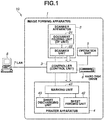
- Fig. 1 is a block diagram illustrating a configuration example of an image forming system 10 according to an exemplary embodiment of the present invention.
- the image forming system 10 is an information processing system, and includes an image forming apparatus 1, a local area network (LAN) 7, and a computer 8.
- the image forming apparatus 1 is an information processing apparatus, and includes a scanner apparatus 2, a controller 3, a printer apparatus 4, an operation unit 5, and a hard disk drive 6.
- the scanner apparatus 2 optically reads an image from a document and converts the document into a digital image.
- the printer apparatus 4 prints the digital image on a paper medium.
- the operation unit 5 performs operation of the image forming apparatus 1.
- the hard disk drive 6 is a nonvolatile storage device that stores the digital image, control programs, etc.
- the controller 3 is a control unit that controls the scanner apparatus 2, the printer apparatus 4, the operation unit 5, and the hard disk drive 6, to execute jobs on the image forming apparatus 1.
- the image forming apparatus 1 inputs or outputs the digital image to and from the external computer 8 through the LAN 7, to perform issuance of a job, instruction to the apparatus, etc.
- the scanner apparatus 2 includes a document feeding unit (DF unit) 21 and a scanner unit 22.
- the document feeding unit 21 automatically and successively feeds a plurality of documents to the scanner unit 22 one by one.
- the scanner unit 22 optically scans the document, converts the document into a digital image, and outputs the converted digital image to the controller 3.
- the printer apparatus 4 includes a marking unit 41, a sheet feeding unit 42, and a sheet discharging unit 43.
- the sheet feeding unit 42 successively feeds a plurality of sheets to the marking unit 41 one by one.
- the marking unit 41 prints the digital image on the fed sheet.
- the sheet discharging unit 43 discharges the printed sheet.
- the operation unit 5 includes an operation button and a display panel such as a liquid crystal display that allow a user to instruct the image forming apparatus 1 to perform operation such as copying of an image, or presents various kinds of information of the image forming apparatus 1 to the user.
- a display panel such as a liquid crystal display that allow a user to instruct the image forming apparatus 1 to perform operation such as copying of an image, or presents various kinds of information of the image forming apparatus 1 to the user.
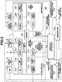
- Fig. 2 is a block diagram illustrating a configuration example of the controller 3 of Fig. 1 .
- the controller 3 includes a main controller 310, a sub-controller 320, a bus bridge 330, a power supply control circuit 331, a power supply unit 340, and a solid state drive (SSD) 314.
- SSD solid state drive
- the main controller 310 includes a main central processing unit (CPU) 311, an internal bus 312, a main CPU memory 313, a read-only memory (ROM) 315, a disk controller 316, a network interface 317, an operation unit interface 318, and a security chip 319.
- the main controller 310 is a general-purpose CPU system.
- the main CPU 311 is a processing unit that controls the whole of the main controller 310.
- the main CPU memory 313 is a volatile storage unit used by the main CPU 311.
- the ROM 315 is a read-only memory.
- the disk controller 316 controls the hard disk drive 6 and the SSD 314.
- the network interface 317 is connected to the LAN 7.
- the operation unit interface 318 is connected to the operation unit 5.
- the security chip 319 is a check unit that internally holds key information for checking an electronic signature, and includes a function of checking an electronic signature of firmware of the image forming apparatus 1.
- the sub-controller 320 includes a sub-CPU 321, an internal bus 322, a sub-CPU memory 323, a scanner interface 324, a printer interface 325, and an image processor 326.
- the sub-CPU 321 is a processing unit that controls the whole of the sub-controller 320.
- the sub-CPU memory 323 is a volatile storage unit used by the sub-CPU 321.
- the scanner interface 324 is connected to the scanner apparatus 2.
- the printer interface 325 is connected to the printer apparatus 4.
- the image processor 326 performs real time digital image processing.
- the bus bridge 330 connects the internal bus 312 of the main controller 310 and the internal bus 322 of the sub-controller 320.
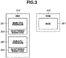
- Fig. 3 is a diagram illustrating stored contents of the SSD 314 and the ROM 315 in Fig. 2 .
- the SSD 314 and the ROM 315 are nonvolatile storage units.
- the SSD 314 stores main CPU firmware 351, an electronic signature 353, sub-CPU firmware 352, and an electronic signature 354.
- the main CPU firmware 351 is a program to operate the main controller 310.
- the main CPU 311 loads the main CPU firmware 351 stored in the SSD 314 into the main CPU memory 313, and executes the main CPU firmware 351 loaded and stored in the main CPU memory 313.
- the sub-CPU firmware 352 is a program to operate the sub-controller 320, and is developed in the sub-CPU memory 323.
- the sub-CPU 321 executes the sub-CPU firmware 352 stored in the sub-CPU memory 323.
- the electronic signature 353 is information for checking that the main CPU firmware 351 is normal (authentic) .
- the electronic signature 354 is information for checking that the sub-CPU firmware 352 is normal.
- the security chip 319 checks that the main CPU firmware 351 is normal based on the electronic signature 353, and checks that the sub-CPU firmware 352 is normal based on the electronic signature 354.
- a state where the firmware is normal (authentic) is, for example, a state where the firmware has not been altered.
- the ROM 315 stores a basic input/output system (BIOS) 361.
- BIOS basic input/output system
- the BIOS 361 is an initial program that is executed first by the main CPU 311 immediately after the image forming apparatus 1 is turned on.
- the firmware 351 and 352 and the electronic signatures 353 and 354 stored in the SSD 314 are rewritable through firmware update, etc.
- the BIOS 361 held by the ROM 315 is unrewritable.
- Each of the main CPU memory 313 and the sub-CPU memory 323 in Fig. 2 is a volatile dynamic random access memory (DRAM), and cannot hold the stored contents while the power of the image forming apparatus is off. Therefore, the main CPU firmware 351 and the sub-CPU firmware 352 are stored in the nonvolatile SSD 314.
- the main CPU firmware 351 is loaded from the SSD 314 into the main CPU memory 313, and the sub-CPU firmware 352 is loaded from the SSD 314 into the sub-CPU memory 323.
- the main CPU 311 executes the main CPU firmware 351 loaded into the main CPU memory 313.
- the sub-CPU 321 executes the sub-CPU firmware 352 loaded into the sub-CPU memory 323.
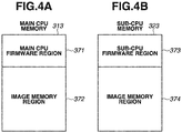
- Fig. 4A is a diagram illustrating a region of the main CPU memory 313.
- the main CPU memory 313 includes a main CPU firmware region 371 and an image memory region 372.
- the main CPU firmware region 371 is a region for storing the main CPU firmware 351 loaded from the SSD 314.
- the main CPU 311 executes the main CPU firmware 351 in the main CPU firmware region 371.
- the image memory region 372 is a region for temporarily storing the image data during job execution.
- Fig. 4B is a diagram illustrating a region of the sub-CPU memory 323.
- the sub-CPU memory 323 includes a sub-CPU firmware region 373 and an image memory region 374.
- the sub-CPU firmware region 373 is a region for storing the sub-CPU firmware 352 loaded from the SSD 314.
- the sub-CPU 321 executes the sub-CPU firmware 352 in the sub-CPU firmware region 373.
- the image memory region 374 is a region for temporarily storing the image data during job execution.
- the power supply control circuit 331 is an electric circuit for controlling a power state of the image forming apparatus 1.
- the power supply unit 340 generates a scanner/printer apparatus power supply voltage 342, a power supply voltage 343 for power-saving state, and a power supply voltage 344 for normal state for the units of the image forming apparatus 1 based on an alternating-current (AC) power supply voltage 341.
- the scanner/printer apparatus power supply voltage 342 is supplied to the scanner apparatus 2 and the printer apparatus 4 through switch control of the power supply control circuit 331.
- the power supply voltage 343 for power-saving state is supplied to the main CPU memory 313, the network interface 317, and the operation unit 5 through the switch control of the power supply control circuit 331.
- the power supply voltage 344 for normal state is supplied to the main controller 310, the sub-controller 320, the SSD 314, and the hard disk drive 6 through the switch control of the power supply control circuit 331.
- a line with an arrow extended from the power supply control circuit 331 indicates a signal line
- a line with an arrow extended from the power supply unit 340 indicates a power supply line.
- the power supply line and the signal line are distinguished by shapes of the respective arrows.
- the scanner/printer apparatus power supply voltage 342 is a power supply voltage supplied to the scanner apparatus 2 and the printer apparatus 4.
- the power supply voltage 343 for power-saving state is a power supply voltage supplied to devices where energization is maintained while the image forming apparatus 1 is in the power-saving state.
- the power supply voltage 344 for normal state is a power supply voltage supplied to devices energized in a case where the image forming apparatus 1 is in the normal state.
- the power supply voltage 344 for normal state is not supplied in the case where the image forming apparatus 1 is in the power-saving state.
- the energized/non-energized states with the power supply voltages are individually controlled by the power supply control circuit 331.
- a power-on signal 332 is a signal to instruct the power supply control circuit 331 to become turned on when the power of the image forming apparatus 1 is off.
- the power-on signal 332 is input when the user operates a power switch inside the operation unit 5.
- a main CPU reset signal 333 is a signal to control a reset state of the main CPU 311.
- a main CPU power-saving cancellation signal 334 is a signal output by the power supply control circuit 331 to cancel the power-saving state of the main CPU 311 in the case where the main CPU 311 is in the power-saving state.
- a sub-CPU reset signal 335 is a signal to control a reset state of the sub-CPU 321.
- the power supply control circuit 331 stops output of the sub-CPU reset signal 335, the reset state of the sub-CPU 321 is canceled and the sub-CPU 321 starts operation.
- the power supply control circuit 331 is connected to the internal bus 312 of the main controller 310, and the main CPU 311 instructs the power supply control circuit 331 to control the state of the sub-CPU reset signal 335.
- a power-saving cancellation signal 336 is a signal to instruct cancellation of the power-saving state when the image forming apparatus 1 is in the power-saving state.
- the controller 3 starts returning operation from the power-saving state to the normal state.
- the power-saving cancellation signal 336 is input to the power supply control circuit 331 in response to operation of the operation unit 5 or packet reception by the network interface 317. More specifically, in a case where the user operates the switch in the operation unit 5, the operation unit 5 outputs the power-saving cancellation signal 336.
- the network interface 317 outputs the power-saving cancellation signal 336 when detecting reception of a network packet from the LAN 7.
- the main CPU 311 stores the digital image data received through the network interface 317, in the image memory region 372 in the main CPU memory 313.
- the main CPU 311 transfers the digital image data to the image memory region 374 in the sub-CPU memory 323. Thereafter, the main CPU 311 instructs the sub-CPU 321 to start printing operation.
- the sub-CPU 321 controls the printer apparatus 4 by outputting an image output instruction to the printer apparatus 4 through the printer interface 325.
- the sub-CPU 321 teaches the image processor 326 a location of the image data in the image memory region 374, and outputs the image data to the printer apparatus 4 through the image processor 326 and the printer interface 325, according to a synchronization signal from the printer apparatus 4.
- the printer apparatus accordingly prints the digital image data on the paper medium.
- the sub-CPU 321 also controls the scanner apparatus 2 in a similar manner.
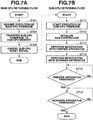
- Figs. 5A and 5B are flowcharts illustrating a method for controlling startup processing of the image forming apparatus 1.
- Fig. 5A is a flowchart illustrating processing executed by the main CPU 311 at the startup of the image forming apparatus 1.
- the power supply control circuit 331 starts supply of the power supply voltages to the units in the image forming apparatus 1. More specifically, the power supply control circuit 331 puts, into a supplied state, all of the scanner/printer apparatus power supply voltage 342, the power supply voltage 343 for power-saving state, and the power supply voltage 344 for normal state.
- the power supply control circuit 331 controls the main CPU reset signal 333 to cancel the reset state of the main CPU 311, the main CPU 311 starts operating and executes the processing of Fig. 5A . At this time, the sub-CPU 321 still remains in the reset state, and the power supply control circuit 331 controls the sub-CPU 321 not to start operation.
- step S501 the main CPU 311 starts execution of the BIOS 361 that is the initial program stored in the ROM 315. Since the BIOS 361 is stored in the unrewritable ROM 315, the BIOS 361 is not rewritten to an unauthorized program.
- step S502 the main CPU 311 executes the BIOS 361 to initialize the disk controller 316. Thereafter, the main CPU 311 controls the SSD 314 to load the main CPU firmware 351 from the SSD 314 to the main CPU firmware region 371 in the main CPU memory 313.
- the main CPU memory 313 stores the main CPU firmware 351 in the main CPU firmware region 371.
- step S503 after loading is completed the main CPU 311 checks whether the main CPU firmware 351 in the main CPU firmware region 371 is normal (authentic). More specifically, the main CPU 311 checks the main CPU firmware 351 based on the electronic signature 353 using an electronic signature check function of the security chip 319.
- step S504 the main CPU 311 determines whether the main CPU firmware 351 is normal, based on a result of the electronic signature check of the main CPU firmware 351. In a case where the main CPU 311 determines that the main CPU firmware 351 is normal (YES in step S504), the processing proceeds to step S505. In a case where the main CPU 311 determines that the main CPU firmware 351 is not normal (NO in step S504), the processing proceeds to step S513.
- step S505 the main CPU 311 starts execution of the main CPU firmware 351 stored in the main CPU firmware region 371.
- step S506 the main CPU 311 executes the main CPU firmware 351 to initialize peripheral devices of the main controller 310. More specifically, the main CPU 311 initializes the network interface 317 and the operation unit interface 318.
- step S507 the main CPU 311 controls the SSD 314 through the disk controller 316, and loads the sub-CPU firmware 352 from the SSD 314 into the image memory region 372 in the main CPU memory 313.
- the image memory region 372 is not used except for the case where the image forming apparatus 1 is executing a job. Therefore, the image memory region 372 is used as a temporal storage of the sub-CPU firmware 352.
- step S508 after loading is completed the main CPU 311 checks whether the sub-CPU firmware 352 in the image memory region 372 is normal. More specifically, the main CPU 311 checks the sub-CPU firmware 352 based on the electronic signature 354 using the electronic signature check function of the security chip 319.
- step S509 the main CPU 311 determines whether the sub-CPU firmware 352 is normal, based on a result of the electronic signature check of the sub-CPU firmware 352. In a case where the main CPU 311 determines that the sub-CPU firmware 352 is normal (YES in step S509), the processing proceeds to step S510. In a case where the main CPU 311 determines that the sub-CPU firmware 352 is not normal (NO in step S509), the processing proceeds to step S512.
- step S510 the main CPU 311 transfers the sub-CPU firmware 352 from the image memory region 372 in the main CPU memory 313 to the sub-CPU firmware region 373 in the sub-CPU memory 323.
- the sub-CPU memory 323 stores the sub-CPU firmware 352 in the sub-CPU firmware region 373.
- step S511 the main CPU 311 controls the sub-CPU reset signal 335 through the power supply control circuit 331 to cancel the reset state of the sub-CPU 321. As a result, the sub-CPU 321 starts the processing of Fig. 5B .
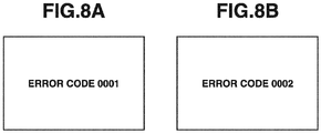
- step S513 the main CPU 311 displays, on the operation unit 5, a screen notifying that the main CPU firmware 351 is not normal. More specifically, as illustrated in Fig. 8A , the main CPU 311 displays, on the screen of the operation unit 5, for example, an error code indicating that the main CPU firmware 351 is abnormal. Fig. 8A illustrates a screen example notifying abnormality. The main CPU 311 then interrupts the startup processing of the image forming apparatus 1.
- step S512 the main CPU 311 displays, on the operation unit 5, a screen notifying that the sub-CPU firmware 352 is not normal. More specifically, as illustrated in Fig. 8B , the main CPU 311 displays, on the screen of the operation unit 5, for example, an error code indicating that the sub-CPU firmware 352 is abnormal. Fig. 8B illustrates a screen example notifying abnormality. The main CPU 311 then interrupts the startup processing of the image forming apparatus 1.
- Fig. 5B is a flowchart illustrating the processing executed by the sub-CPU 321 at the startup of the image forming apparatus 1.
- the sub-CPU 321 starts execution of the processing of Fig. 5B .
- step S521 the sub-CPU 321 starts execution of the sub-CPU firmware 352 stored in the sub-CPU firmware region 373. As described above, the sub-CPU firmware 352 has been previously determined to be normal by the main CPU 311.
- step S522 the sub-CPU 321 initializes the peripheral devices in the sub-controller 320. More specifically, the sub-CPU 321 initializes the scanner interface 324, the printer interface 325, and the image processor 326.
- step S523 the sub-CPU 321 performs negotiation with the printer apparatus 4 through the printer interface 325.
- step S524 the sub-CPU 321 performs negotiation with the scanner apparatus 2 through the scanner interface 324.
- step S525 the sub-CPU 321 determines whether preparation for job execution of the printer apparatus 4 has been completed.
- the printer apparatus 4 After the negotiation in step S523, the printer apparatus 4 performs various kinds of adjusting operation, and it is necessary for the sub-CPU 321 to wait for completion of the adjusting operation for job execution.
- the sub-CPU 321 can know, through the printer interface 325, whether the preparation of the printer apparatus 4 has been completed. Therefore, the sub-CPU 321 repeats the process in step S525 until the preparation of the printer 4 is completed. In a case where the sub-CPU 321 determines that the preparation of the printer apparatus 4 has been completed (YES in step S525), the processing proceeds to step S526.
- step S526 the sub-CPU 321 determines whether preparation for job execution of the scanner apparatus 2 has been completed, in a similar manner.
- the sub-CPU 321 repeats the process in step S526 until the preparation of the scanner apparatus 2 is completed.
- the startup processing of the image forming apparatus 1 is ended.
- the main CPU 311 checks the electronic signature 353 of the main CPU firmware 351 and the electronic signature 354 of the sub-CPU firmware 352.
- the sub-CPU 321 executes the startup processing of Fig. 5B only in the case where the main CPU 311 determines that the electronic signature 353 and the electronic signature 354are normal. This makes it possible to ensure that the main CPU 311 and the sub-CPU 321 do not execute unauthorized firmware at the startup of the image forming apparatus 1, and to secure safety.
- the checking of whether the main CPU firmware 351 and the sub-CPU firmware 352 are authorized is performed using the electronic signature technology; however, the configuration is an example.
- Hash values of the main CPU firmware 351 and the sub-CPU firmware 352 may be previously stored in a nonvolatile storage medium, rewriting of which is difficult.
- the checking may be performed by, for example, a method for comparing the stored hash values of the main CPU firmware 351 and the sub-CPU firmware 352 calculated at the startup with each other.
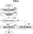
- Fig. 6 is a flowchart indicating processing executed by the main CPU 311 when the image forming apparatus 1 makes a transition from the normal state (first power mode) to the power-saving state (second power mode).
- the image forming apparatus 1 executes the processing of Fig. 6 .
- the image forming apparatus 1 executes the processing of Fig. 6 .
- the image forming apparatus 1 makes a transition from the normal state to the power-saving state to save power.
- step S601 the main CPU 311 controls the SSD 314 through the disk controller 316, and loads the sub-CPU firmware 352 from the SSD 314 to the image memory region 372 in the main CPU memory 313.
- the sub-CPU firmware 352 is used when the image forming apparatus 1 is returned from the power-saving state to the normal state afterward.
- the image memory region 372 is not used because the image forming apparatus 1 does not execute a job, and is accordingly used as a temporal storage of the sub-CPU firmware 352.
- step S602 after loading is completed the main CPU 311 checks whether the sub-CPU firmware 352 in the image memory region 372 is normal (authentic). More specifically, the main CPU 311 checks the sub-CPU firmware 352 based on the electronic signature 354 using the electronic signature check function of the security chip 319.
- step S603 the main CPU 311 determines whether the sub-CPU firmware 352 is normal, based on a result of the electronic signature checking of the sub-CPU firmware 352. In a case where the main CPU 311 determines that the sub-CPU firmware 352 is normal (YES in step S603), the processing proceeds to step S604. In a case where the main CPU 311 determines that the sub-CPU firmware 352 is not normal (NO in step S603), the processing proceeds to step S605. The case where the main CPU 311 determines that the sub-CPU firmware 352 is normal corresponds to a case where the main CPU 311 confirms that the sub-CPU firmware 352 is authentic.
- step S604 the main CPU 311 controls the power supply control circuit 331 to cause the image forming apparatus 1 to make a transition to the power-saving state.
- the power supply control circuit 331 stops supply of the scanner/printer apparatus power supply voltage 342 and the power supply voltage 344 for normal state, and maintains supply of the power supply voltage 343 for power-saving state. As a result, the image forming apparats 1 transitions to the power-saving state.
- Fig. 9 is a diagram illustrating an energized state of each of the units of the image forming apparatus 1 in the power-saving state.
- the power supply control circuit 331 supplies the power supply voltage 343 for power-saving state to the main CPU memory 313, the network interface 317, and the operation unit 5. In contrast, the power supply control circuit 331 does not supply the power supply voltage 343 for power-saving state to the main CPU 311, the sub-CPU 321, the sub-CPU memory 323, the SSD 314, etc.
- the main CPU memory 313, the network interface 317, the operation unit 5, the power supply control circuit 331, and the power supply unit 340 are in the energized state. Other units are in a non-energized state.
- the main CPU memory 313 is maintained in the energized state and holds the sub-CPU firmware 352 in the image memory region 372 while the image forming apparatus 1 is in the power-saving state. In such a manner, in the power-saving state, the energization of the hard disk drive 6 and the sub-CPU memory 323 is stopped, and the energization of the main CPU memory 313 is not stopped.
- step S605 of Fig. 6 the main CPU 311 displays, on the operation unit 5, the screen notifying that the sub-CPU firmware 352 is not normal, as illustrated in Fig. 8B .
- the main CPU 311 then interrupts the transition processing for the image forming apparatus 1 to transition to the power-saving state.
- the image forming apparatus 1 makes a transition from the normal state to the power-saving state through the processing of Fig. 6 .
- the main CPU 311 cancels the transition to the power-saving state. This makes it possible to prevent the unauthorized sub-CPU firmware 352 from being executed by the sub-CPU 321 when the image forming apparatus 1 returns from the power-saving state to the normal state.
- Figs. 7A and 7B are flowcharts illustrating processing when the image forming apparatus 1 returns from the power-saving state to the normal state.
- Fig. 7A is a flowchart illustrating the returning processing for the main CPU 311 to return the normal state.
- the image forming apparatus 1 executes the processing of Figs. 7A and 7B .
- the power supply control circuit 331 receives the power-saving cancellation signal 336.
- the power supply control circuit 331 then supplies the scanner/printer apparatus power supply voltage 342 and the power supply voltage 344 for normal state to the units of the image forming apparatus 1, outputs the main CPU power-saving cancellation signal 334 to the main CPU 311, thereby resuming the operation of the main CPU 311. More specifically, the power supply control circuit 331 supplies the power supply voltage 344 for normal state to the main CPU 311, the main CPU memory 313, the sub-CPU 321, the sub-CPU memory 323, the SSD 314, etc. The CPU 311, after resuming the operation, executes the processing of Fig. 7A .
- step S701 the main CPU 311 resumes execution of the main CPU firmware 351 in the main CPU firmware region 371.
- the main CPU memory 313 is energized and holds the stored contents while the image forming apparatus is in the power-saving state.
- step S702 the main CPU 311 transfers the sub-CPU firmware 352 in the image memory region 372 to the sub-CPU firmware region 373 in the sub-CPU memory 323.
- the Sub-CPU memory 323 has lost the stored contents because the energization of the sub-CPU memory 323 is stopped while the image forming apparatus 1 is in the power-saving state. Therefore, to bring the sub-controller 320 into an operating state again, it is necessary for the main CPU 311 to transfer the sub-CPU firmware 352 to the sub-CPU memory 323.
- the main CPU 311 transfers the sub-CPU firmware 352 that has been checked in step S602 of Fig. 6 at the transition to the power-saving state.
- the main CPU 311 may load the sub-CPU firmware 352 from the SSD 314 to the main CPU memory 313 and transfer the sub-CPU firmware 352 from the main CPU memory 313 to the sub-CPU memory 323 at the time of returning to the normal state. In this case, however, it takes a long time for the image forming apparatus 1 to return from the power-saving state to the normal state.
- the main CPU 313 loads the sub-CPU firmware 352 from the SSD 314 to the main CPU memory 313 at the transition to the power-saving state in Fig. 6 .
- the main CPU 311 transfers the sub-CPU firmware 352 from the main CPU memory 313 to the sub-CPU memory 323 at the time of returning to the normal state in Fig. 7A . This allows a reduction in the returning time taken for the image forming apparatus 1 to return from the power-saving state to the normal state.
- step S703 the main CPU 311 controls the sub-CPU reset signal 335 through the power supply control circuit 331 to cancel the reset state of the sub-CPU 321.
- the sub-CPU 321 starts the processing of Fig. 7B .
- Fig. 7B is a flowchart illustrating the processing executed by the sub-CPU 321 at the time of returning from the power-saving state to the normal state.
- the sub-CPU 321 of which the reset state has been canceled in step S703 of Fig. 7A starts execution of the processing of Fig. 7B .
- the sub-CPU 321 performs processes in steps S711 to S716.
- the processes in steps S711 to S716 are the same as the processes in steps S521 to S526 of Fig. 5B , and therefore the description thereof is omitted.
- the image forming apparatus 1 returns from the power-saving state to the normal state through the processing of Figs. 7A and 7B .
- the sub-CPU 321 can execute the sub-CPU firmware 352 that has been confirmed to be not unauthorized firmware through the checking, at the time when the image forming apparatus 1 returns from the power-saving state to the normal state. This allows the sub-CPU 321 to prevent from executing unauthorized sub-CPU firmware 352 not only when the image forming apparatus 1 is started up but also when the image forming apparatus 1 returns from the power-saving state to the normal state. As a result, it is possible to improve security of the image forming apparatus 1.
- the main CPU 311 previously checks on the sub-CPU firmware 352 at the transition to the power-saving state, which allows the main CPU 311 to prevent execution of the unauthorized sub-CPU firmware 352, thereby reducing a time necessary for returning from the power-saving state to the normal state. Since it does not deteriorate the convenience of the image forming apparatus 1 in returning from the power-saving state to the normal state is not deteriorated, it makes it possible to achieve both of security and convenience of the image forming apparatus 1 thereby. Moreover, the power supply control circuit 331 stops supply of the power supply voltage to the sub-controller 320 to reduce power consumption in the power-saving state.
- main CPU firmware 531 and the sub-CPU firmware 352 are stored in the SSD 314 has been described as an example; however, the configuration is not limited thereto, and the main CPU firmware 531 and the sub-CPU firmware 352 may be stored in other nonvolatile storage medium such as the hard disk drive 6. Further, the main CPU firmware 531 and the sub-CPU firmware 352 may be stored in different nonvolatile storage media.
- Embodiment(s) of the present invention can also be realized by a computer of a system or apparatus that reads out and executes computer executable instructions (e.g., one or more programs) recorded on a storage medium (which may also be referred to more fully as a 'non-transitory computer-readable storage medium') to perform the functions of one or more of the above-described embodiment(s) and/or that includes one or more circuits (e.g., application specific integrated circuit (ASIC)) for performing the functions of one or more of the above-described embodiment(s), and by a method performed by the computer of the system or apparatus by, for example, reading out and executing the computer executable instructions from the storage medium to perform the functions of one or more of the above-described embodiment(s) and/or controlling the one or more circuits to perform the functions of one or more of the above-described embodiment(s).
- computer executable instructions e.g., one or more programs
- a storage medium which may also be referred to more fully as
- the computer may comprise one or more processors (e.g., central processing unit (CPU), micro processing unit (MPU)) and may include a network of separate computers or separate processors to read out and execute the computer executable instructions.
- the computer executable instructions may be provided to the computer, for example, from a network or the storage medium.
- the storage medium may include, for example, one or more of a hard disk, a random-access memory (RAM), a read only memory (ROM), a storage of distributed computing systems, an optical disk (such as a compact disc (CD), digital versatile disc (DVD), or Blu-ray Disc (BD)TM), a flash memory device, a memory card, and the like.
Description
- The present invention relates to an information processing apparatus and a method for controlling the information processing apparatus.
- Japanese Patent Application Laid-Open No.
2009-223866 - A nonvolatile program storage unit stores a first program executed by a first central processing unit (CPU) and a second program executed by a second CPU. The first CPU executes the first program loaded from the program storage unit to a first memory. The second CPU executes the second program loaded from the program storage unit to a volatile second memory.
- In a case where a condition for transition to the power-saving mode is satisfied, the second program is transferred from the program storage unit to the first memory. In the case where the condition for transition to the power-saving mode is satisfied, power supply to the second memory is stopped. In a case where a condition for returning to the normal power mode is satisfied, the information processing apparatus resumes the supply of power to the second memory and makes a transition to the normal power mode. In the case where the condition for returning to the normal power mode is satisfied, the second program held by the first memory is transferred to the second memory. In the case where the condition for returning to the normal power mode is satisfied, the second CPU executes the second program if the second program has been transferred to the second memory.
- The information processing apparatus discussed in Japanese Patent Application Laid-Open No.
2009-223866 - If the program stored by the nonvolatile storage unit is altered during the power-saving mode, and the mode is shifted from the power-saving mode to the normal power mode, and then from a first power mode to a second power mode, the altered second program is transferred from the nonvolatile storage unit to the first memory. Thereafter, when the mode is shifted from the power-saving mode to the normal power mode, the altered second program stored in the first memory is transferred to the second memory, and a second calculation unit executes the alternated second program stored in the second memory.
- Document
US 6 901 298 B1 discloses a system and methodology for saving and restoring controller state and context in an industrial controller according to the preamble of claim 1. Further background information of the present invention is provided in documentUS 2009/207423 A1 and documentUS 2017/177870 A1 . - Document
US 2015/124279 A1 discloses an image forming apparatus, having a main controller for controlling access to a main memory. This document discloses to determine whether the main memory is a non-volatile memory or a volatile memory, and store the result of the determination in non-volatile memory, and, erase data stored in the main memory when transition is made to a power off state or a sleep mode when it is determined that the main memory is a non-volatile memory. - According to a first aspect of the present invention, there is provided an information processing apparatus as specified in claims 1 to 11. According to a second aspect of the present invention there is provided a control method as specified in claim 12. Further aspects of the invention are outlined in the dependent claims. When the term embodiment is used for describing unclaimed combination of features, the term has to be understood as referring to examples useful for understanding the present invention.
- Further features of the present invention will become apparent from the following description of exemplary embodiments with reference to the attached drawings.
-
-
Fig. 1 is a block diagram illustrating a configuration example of an image forming system. -
Fig. 2 is a block diagram illustrating a configuration example of a controller. -
Fig. 3 is a diagram illustrating an arrangement of firmware of an image forming apparatus. -
Figs. 4A and 4B are diagrams each illustrating a configuration example of a memory of the image forming apparatus. -
Figs. 5A and 5B are flowcharts illustrating startup operation of the image forming apparatus. -
Fig. 6 is a flowchart illustrating transition operation to a power-saving state of the image forming apparatus. -
Figs. 7A and 7B are flowcharts illustrating returning operation to a normal state of the image forming apparatus. -
Figs. 8A and 8B are diagrams each illustrating a screen example displayed when firmware abnormality is detected. -
Fig. 9 is a diagram illustrating an energized state of the image forming apparatus in the power-saving state. -
Fig. 1 is a block diagram illustrating a configuration example of animage forming system 10 according to an exemplary embodiment of the present invention. Theimage forming system 10 is an information processing system, and includes an image forming apparatus 1, a local area network (LAN) 7, and acomputer 8. The image forming apparatus 1 is an information processing apparatus, and includes ascanner apparatus 2, acontroller 3, aprinter apparatus 4, anoperation unit 5, and ahard disk drive 6. Thescanner apparatus 2 optically reads an image from a document and converts the document into a digital image. Theprinter apparatus 4 prints the digital image on a paper medium. Theoperation unit 5 performs operation of the image forming apparatus 1. Thehard disk drive 6 is a nonvolatile storage device that stores the digital image, control programs, etc. Thecontroller 3 is a control unit that controls thescanner apparatus 2, theprinter apparatus 4, theoperation unit 5, and thehard disk drive 6, to execute jobs on the image forming apparatus 1. The image forming apparatus 1 inputs or outputs the digital image to and from theexternal computer 8 through theLAN 7, to perform issuance of a job, instruction to the apparatus, etc. - The
scanner apparatus 2 includes a document feeding unit (DF unit) 21 and ascanner unit 22. Thedocument feeding unit 21 automatically and successively feeds a plurality of documents to thescanner unit 22 one by one. Thescanner unit 22 optically scans the document, converts the document into a digital image, and outputs the converted digital image to thecontroller 3. - The
printer apparatus 4 includes amarking unit 41, asheet feeding unit 42, and asheet discharging unit 43. Thesheet feeding unit 42 successively feeds a plurality of sheets to themarking unit 41 one by one. Themarking unit 41 prints the digital image on the fed sheet. Thesheet discharging unit 43 discharges the printed sheet. - The
operation unit 5 includes an operation button and a display panel such as a liquid crystal display that allow a user to instruct the image forming apparatus 1 to perform operation such as copying of an image, or presents various kinds of information of the image forming apparatus 1 to the user. -
Fig. 2 is a block diagram illustrating a configuration example of thecontroller 3 ofFig. 1 . Thecontroller 3 includes amain controller 310, asub-controller 320, abus bridge 330, a powersupply control circuit 331, apower supply unit 340, and a solid state drive (SSD) 314. - The
main controller 310 includes a main central processing unit (CPU) 311, aninternal bus 312, amain CPU memory 313, a read-only memory (ROM) 315, adisk controller 316, anetwork interface 317, anoperation unit interface 318, and asecurity chip 319. Themain controller 310 is a general-purpose CPU system. Themain CPU 311 is a processing unit that controls the whole of themain controller 310. Themain CPU memory 313 is a volatile storage unit used by themain CPU 311. TheROM 315 is a read-only memory. Thedisk controller 316 controls thehard disk drive 6 and theSSD 314. Thenetwork interface 317 is connected to theLAN 7. Theoperation unit interface 318 is connected to theoperation unit 5. Thesecurity chip 319 is a check unit that internally holds key information for checking an electronic signature, and includes a function of checking an electronic signature of firmware of the image forming apparatus 1. - The sub-controller 320 includes a sub-CPU 321, an
internal bus 322, asub-CPU memory 323, ascanner interface 324, aprinter interface 325, and animage processor 326. Thesub-CPU 321 is a processing unit that controls the whole of the sub-controller 320. Thesub-CPU memory 323 is a volatile storage unit used by thesub-CPU 321. Thescanner interface 324 is connected to thescanner apparatus 2. Theprinter interface 325 is connected to theprinter apparatus 4. Theimage processor 326 performs real time digital image processing. Thebus bridge 330 connects theinternal bus 312 of themain controller 310 and theinternal bus 322 of the sub-controller 320. -
Fig. 3 is a diagram illustrating stored contents of theSSD 314 and theROM 315 inFig. 2 . TheSSD 314 and theROM 315 are nonvolatile storage units. TheSSD 314 storesmain CPU firmware 351, anelectronic signature 353,sub-CPU firmware 352, and anelectronic signature 354. Themain CPU firmware 351 is a program to operate themain controller 310. Themain CPU 311 loads themain CPU firmware 351 stored in theSSD 314 into themain CPU memory 313, and executes themain CPU firmware 351 loaded and stored in themain CPU memory 313. Thesub-CPU firmware 352 is a program to operate the sub-controller 320, and is developed in thesub-CPU memory 323. Thesub-CPU 321 executes thesub-CPU firmware 352 stored in thesub-CPU memory 323. - The
electronic signature 353 is information for checking that themain CPU firmware 351 is normal (authentic) . Theelectronic signature 354 is information for checking that thesub-CPU firmware 352 is normal. Thesecurity chip 319 checks that themain CPU firmware 351 is normal based on theelectronic signature 353, and checks that thesub-CPU firmware 352 is normal based on theelectronic signature 354. A state where the firmware is normal (authentic) is, for example, a state where the firmware has not been altered. - The
ROM 315 stores a basic input/output system (BIOS) 361. TheBIOS 361 is an initial program that is executed first by themain CPU 311 immediately after the image forming apparatus 1 is turned on. Thefirmware electronic signatures SSD 314 are rewritable through firmware update, etc. In contrast, theBIOS 361 held by theROM 315 is unrewritable. - Each of the
main CPU memory 313 and thesub-CPU memory 323 inFig. 2 is a volatile dynamic random access memory (DRAM), and cannot hold the stored contents while the power of the image forming apparatus is off. Therefore, themain CPU firmware 351 and thesub-CPU firmware 352 are stored in thenonvolatile SSD 314. When the image forming apparatus 1 is turned on, themain CPU firmware 351 is loaded from theSSD 314 into themain CPU memory 313, and thesub-CPU firmware 352 is loaded from theSSD 314 into thesub-CPU memory 323. Themain CPU 311 executes themain CPU firmware 351 loaded into themain CPU memory 313. Thesub-CPU 321 executes thesub-CPU firmware 352 loaded into thesub-CPU memory 323. -
Fig. 4A is a diagram illustrating a region of themain CPU memory 313. Themain CPU memory 313 includes a mainCPU firmware region 371 and animage memory region 372. The mainCPU firmware region 371 is a region for storing themain CPU firmware 351 loaded from theSSD 314. Themain CPU 311 executes themain CPU firmware 351 in the mainCPU firmware region 371. Theimage memory region 372 is a region for temporarily storing the image data during job execution. -
Fig. 4B is a diagram illustrating a region of thesub-CPU memory 323. Thesub-CPU memory 323 includes asub-CPU firmware region 373 and animage memory region 374. Thesub-CPU firmware region 373 is a region for storing thesub-CPU firmware 352 loaded from theSSD 314. Thesub-CPU 321 executes thesub-CPU firmware 352 in thesub-CPU firmware region 373. Theimage memory region 374 is a region for temporarily storing the image data during job execution. - In
Fig. 2 , the powersupply control circuit 331 is an electric circuit for controlling a power state of the image forming apparatus 1. Thepower supply unit 340 generates a scanner/printer apparatuspower supply voltage 342, apower supply voltage 343 for power-saving state, and apower supply voltage 344 for normal state for the units of the image forming apparatus 1 based on an alternating-current (AC)power supply voltage 341. The scanner/printer apparatuspower supply voltage 342 is supplied to thescanner apparatus 2 and theprinter apparatus 4 through switch control of the powersupply control circuit 331. Thepower supply voltage 343 for power-saving state is supplied to themain CPU memory 313, thenetwork interface 317, and theoperation unit 5 through the switch control of the powersupply control circuit 331. Thepower supply voltage 344 for normal state is supplied to themain controller 310, the sub-controller 320, theSSD 314, and thehard disk drive 6 through the switch control of the powersupply control circuit 331. InFig. 2 , a line with an arrow extended from the powersupply control circuit 331 indicates a signal line, and a line with an arrow extended from thepower supply unit 340 indicates a power supply line. InFig. 2 , the power supply line and the signal line are distinguished by shapes of the respective arrows. - The scanner/printer apparatus
power supply voltage 342 is a power supply voltage supplied to thescanner apparatus 2 and theprinter apparatus 4. Thepower supply voltage 343 for power-saving state is a power supply voltage supplied to devices where energization is maintained while the image forming apparatus 1 is in the power-saving state. Thepower supply voltage 344 for normal state is a power supply voltage supplied to devices energized in a case where the image forming apparatus 1 is in the normal state. Thepower supply voltage 344 for normal state is not supplied in the case where the image forming apparatus 1 is in the power-saving state. The energized/non-energized states with the power supply voltages are individually controlled by the powersupply control circuit 331. - A power-on
signal 332 is a signal to instruct the powersupply control circuit 331 to become turned on when the power of the image forming apparatus 1 is off. The power-onsignal 332 is input when the user operates a power switch inside theoperation unit 5. A mainCPU reset signal 333 is a signal to control a reset state of themain CPU 311. When the powersupply control circuit 331 stops output of the mainCPU reset signal 333 in response to power-on of the image forming apparatus 1, the reset state of themain CPU 311 is canceled and themain CPU 311 starts operation. A main CPU power-savingcancellation signal 334 is a signal output by the powersupply control circuit 331 to cancel the power-saving state of themain CPU 311 in the case where themain CPU 311 is in the power-saving state. - A
sub-CPU reset signal 335 is a signal to control a reset state of thesub-CPU 321. When the powersupply control circuit 331 stops output of thesub-CPU reset signal 335, the reset state of thesub-CPU 321 is canceled and the sub-CPU 321 starts operation. The powersupply control circuit 331 is connected to theinternal bus 312 of themain controller 310, and themain CPU 311 instructs the powersupply control circuit 331 to control the state of thesub-CPU reset signal 335. - A power-saving
cancellation signal 336 is a signal to instruct cancellation of the power-saving state when the image forming apparatus 1 is in the power-saving state. When the power-savingcancellation signal 336 is input to the powersupply control circuit 331, thecontroller 3 starts returning operation from the power-saving state to the normal state. The power-savingcancellation signal 336 is input to the powersupply control circuit 331 in response to operation of theoperation unit 5 or packet reception by thenetwork interface 317. More specifically, in a case where the user operates the switch in theoperation unit 5, theoperation unit 5 outputs the power-savingcancellation signal 336. In addition, thenetwork interface 317 outputs the power-savingcancellation signal 336 when detecting reception of a network packet from theLAN 7. - Next, operation of the
controller 3 is described with printing operation using a paper medium as an example. When thenetwork interface 317 receives a print job from theLAN 7, themain CPU 311 stores the digital image data received through thenetwork interface 317, in theimage memory region 372 in themain CPU memory 313. When it is confirmed that a certain amount or all of the digital image data is stored in theimage memory region 372, themain CPU 311 transfers the digital image data to theimage memory region 374 in thesub-CPU memory 323. Thereafter, themain CPU 311 instructs the sub-CPU 321 to start printing operation. - The sub-CPU 321 controls the
printer apparatus 4 by outputting an image output instruction to theprinter apparatus 4 through theprinter interface 325. Thesub-CPU 321 teaches the image processor 326 a location of the image data in theimage memory region 374, and outputs the image data to theprinter apparatus 4 through theimage processor 326 and theprinter interface 325, according to a synchronization signal from theprinter apparatus 4. The printer apparatus accordingly prints the digital image data on the paper medium. The sub-CPU 321 also controls thescanner apparatus 2 in a similar manner. -
Figs. 5A and 5B are flowcharts illustrating a method for controlling startup processing of the image forming apparatus 1.Fig. 5A is a flowchart illustrating processing executed by themain CPU 311 at the startup of the image forming apparatus 1. When the power-onsignal 332 is provided, the powersupply control circuit 331 starts supply of the power supply voltages to the units in the image forming apparatus 1. More specifically, the powersupply control circuit 331 puts, into a supplied state, all of the scanner/printer apparatuspower supply voltage 342, thepower supply voltage 343 for power-saving state, and thepower supply voltage 344 for normal state. When the powersupply control circuit 331 controls the mainCPU reset signal 333 to cancel the reset state of themain CPU 311, themain CPU 311 starts operating and executes the processing ofFig. 5A . At this time, the sub-CPU 321 still remains in the reset state, and the powersupply control circuit 331 controls the sub-CPU 321 not to start operation. - In step S501, the
main CPU 311 starts execution of theBIOS 361 that is the initial program stored in theROM 315. Since theBIOS 361 is stored in theunrewritable ROM 315, theBIOS 361 is not rewritten to an unauthorized program. - Next, in step S502, the
main CPU 311 executes theBIOS 361 to initialize thedisk controller 316. Thereafter, themain CPU 311 controls theSSD 314 to load themain CPU firmware 351 from theSSD 314 to the mainCPU firmware region 371 in themain CPU memory 313. Themain CPU memory 313 stores themain CPU firmware 351 in the mainCPU firmware region 371. - In step S503 after loading is completed, the
main CPU 311 checks whether themain CPU firmware 351 in the mainCPU firmware region 371 is normal (authentic). More specifically, themain CPU 311 checks themain CPU firmware 351 based on theelectronic signature 353 using an electronic signature check function of thesecurity chip 319. - Next, in step S504, the
main CPU 311 determines whether themain CPU firmware 351 is normal, based on a result of the electronic signature check of themain CPU firmware 351. In a case where themain CPU 311 determines that themain CPU firmware 351 is normal (YES in step S504), the processing proceeds to step S505. In a case where themain CPU 311 determines that themain CPU firmware 351 is not normal (NO in step S504), the processing proceeds to step S513. - In step S505, the
main CPU 311 starts execution of themain CPU firmware 351 stored in the mainCPU firmware region 371. Next, in step S506, themain CPU 311 executes themain CPU firmware 351 to initialize peripheral devices of themain controller 310. More specifically, themain CPU 311 initializes thenetwork interface 317 and theoperation unit interface 318. - Next, in step S507, the
main CPU 311 controls theSSD 314 through thedisk controller 316, and loads thesub-CPU firmware 352 from theSSD 314 into theimage memory region 372 in themain CPU memory 313. Theimage memory region 372 is not used except for the case where the image forming apparatus 1 is executing a job. Therefore, theimage memory region 372 is used as a temporal storage of thesub-CPU firmware 352. - In step S508 after loading is completed, the
main CPU 311 checks whether thesub-CPU firmware 352 in theimage memory region 372 is normal. More specifically, themain CPU 311 checks thesub-CPU firmware 352 based on theelectronic signature 354 using the electronic signature check function of thesecurity chip 319. - Next, in step S509, the
main CPU 311 determines whether thesub-CPU firmware 352 is normal, based on a result of the electronic signature check of thesub-CPU firmware 352. In a case where themain CPU 311 determines that thesub-CPU firmware 352 is normal (YES in step S509), the processing proceeds to step S510. In a case where themain CPU 311 determines that thesub-CPU firmware 352 is not normal (NO in step S509), the processing proceeds to step S512. - In step S510, the
main CPU 311 transfers thesub-CPU firmware 352 from theimage memory region 372 in themain CPU memory 313 to thesub-CPU firmware region 373 in thesub-CPU memory 323. Thesub-CPU memory 323 stores thesub-CPU firmware 352 in thesub-CPU firmware region 373. Next, in step S511, themain CPU 311 controls the sub-CPU reset signal 335 through the powersupply control circuit 331 to cancel the reset state of thesub-CPU 321. As a result, the sub-CPU 321 starts the processing ofFig. 5B . - In step S513, the
main CPU 311 displays, on theoperation unit 5, a screen notifying that themain CPU firmware 351 is not normal. More specifically, as illustrated inFig. 8A , themain CPU 311 displays, on the screen of theoperation unit 5, for example, an error code indicating that themain CPU firmware 351 is abnormal.Fig. 8A illustrates a screen example notifying abnormality. Themain CPU 311 then interrupts the startup processing of the image forming apparatus 1. - In step S512, the
main CPU 311 displays, on theoperation unit 5, a screen notifying that thesub-CPU firmware 352 is not normal. More specifically, as illustrated inFig. 8B , themain CPU 311 displays, on the screen of theoperation unit 5, for example, an error code indicating that thesub-CPU firmware 352 is abnormal.Fig. 8B illustrates a screen example notifying abnormality. Themain CPU 311 then interrupts the startup processing of the image forming apparatus 1. -
Fig. 5B is a flowchart illustrating the processing executed by the sub-CPU 321 at the startup of the image forming apparatus 1. When the reset state of thesub-CPU 321 is canceled in step S511 ofFig. 5A , the sub-CPU 321 starts execution of the processing ofFig. 5B . - In step S521, the sub-CPU 321 starts execution of the
sub-CPU firmware 352 stored in thesub-CPU firmware region 373. As described above, thesub-CPU firmware 352 has been previously determined to be normal by themain CPU 311. - Next, in step S522, the
sub-CPU 321 initializes the peripheral devices in the sub-controller 320. More specifically, thesub-CPU 321 initializes thescanner interface 324, theprinter interface 325, and theimage processor 326. - Next, in step S523, the
sub-CPU 321 performs negotiation with theprinter apparatus 4 through theprinter interface 325. Next, in step S524, thesub-CPU 321 performs negotiation with thescanner apparatus 2 through thescanner interface 324. - Next, in step S525, the
sub-CPU 321 determines whether preparation for job execution of theprinter apparatus 4 has been completed. After the negotiation in step S523, theprinter apparatus 4 performs various kinds of adjusting operation, and it is necessary for the sub-CPU 321 to wait for completion of the adjusting operation for job execution. The sub-CPU 321 can know, through theprinter interface 325, whether the preparation of theprinter apparatus 4 has been completed. Therefore, the sub-CPU 321 repeats the process in step S525 until the preparation of theprinter 4 is completed. In a case where thesub-CPU 321 determines that the preparation of theprinter apparatus 4 has been completed (YES in step S525), the processing proceeds to step S526. - In step S526, the
sub-CPU 321 determines whether preparation for job execution of thescanner apparatus 2 has been completed, in a similar manner. The sub-CPU 321 repeats the process in step S526 until the preparation of thescanner apparatus 2 is completed. In a case where thesub-CPU 321 determines that the preparation of thescanner apparatus 2 has been completed (YES in step S526), the startup processing of the image forming apparatus 1 is ended. - At the startup of the image forming apparats 1, the
main CPU 311 checks theelectronic signature 353 of themain CPU firmware 351 and theelectronic signature 354 of thesub-CPU firmware 352. Thesub-CPU 321 executes the startup processing ofFig. 5B only in the case where themain CPU 311 determines that theelectronic signature 353 and the electronic signature 354are normal. This makes it possible to ensure that themain CPU 311 and the sub-CPU 321 do not execute unauthorized firmware at the startup of the image forming apparatus 1, and to secure safety. - In the present exemplary embodiment, the checking of whether the
main CPU firmware 351 and thesub-CPU firmware 352 are authorized is performed using the electronic signature technology; however, the configuration is an example. Hash values of themain CPU firmware 351 and thesub-CPU firmware 352 may be previously stored in a nonvolatile storage medium, rewriting of which is difficult. In this case, the checking may be performed by, for example, a method for comparing the stored hash values of themain CPU firmware 351 and thesub-CPU firmware 352 calculated at the startup with each other. -
Fig. 6 is a flowchart indicating processing executed by themain CPU 311 when the image forming apparatus 1 makes a transition from the normal state (first power mode) to the power-saving state (second power mode). In a case where a condition for transitioning from the normal state to the power-saving state is satisfied, the image forming apparatus 1 executes the processing ofFig. 6 . For example, in a case where no job is executed for a predetermined time or more, the image forming apparatus 1 executes the processing ofFig. 6 . The image forming apparatus 1 makes a transition from the normal state to the power-saving state to save power. - First, in step S601, the
main CPU 311 controls theSSD 314 through thedisk controller 316, and loads thesub-CPU firmware 352 from theSSD 314 to theimage memory region 372 in themain CPU memory 313. Thesub-CPU firmware 352 is used when the image forming apparatus 1 is returned from the power-saving state to the normal state afterward. When themain CPU 311 executes the transition processing to the power-saving state, theimage memory region 372 is not used because the image forming apparatus 1 does not execute a job, and is accordingly used as a temporal storage of thesub-CPU firmware 352. - In step S602 after loading is completed, the
main CPU 311 checks whether thesub-CPU firmware 352 in theimage memory region 372 is normal (authentic). More specifically, themain CPU 311 checks thesub-CPU firmware 352 based on theelectronic signature 354 using the electronic signature check function of thesecurity chip 319. - Next, in step S603, the
main CPU 311 determines whether thesub-CPU firmware 352 is normal, based on a result of the electronic signature checking of thesub-CPU firmware 352. In a case where themain CPU 311 determines that thesub-CPU firmware 352 is normal (YES in step S603), the processing proceeds to step S604. In a case where themain CPU 311 determines that thesub-CPU firmware 352 is not normal (NO in step S603), the processing proceeds to step S605. The case where themain CPU 311 determines that thesub-CPU firmware 352 is normal corresponds to a case where themain CPU 311 confirms that thesub-CPU firmware 352 is authentic. - In step S604, the
main CPU 311 controls the powersupply control circuit 331 to cause the image forming apparatus 1 to make a transition to the power-saving state. The powersupply control circuit 331 stops supply of the scanner/printer apparatuspower supply voltage 342 and thepower supply voltage 344 for normal state, and maintains supply of thepower supply voltage 343 for power-saving state. As a result, the image forming apparats 1 transitions to the power-saving state. -
Fig. 9 is a diagram illustrating an energized state of each of the units of the image forming apparatus 1 in the power-saving state. The powersupply control circuit 331 supplies thepower supply voltage 343 for power-saving state to themain CPU memory 313, thenetwork interface 317, and theoperation unit 5. In contrast, the powersupply control circuit 331 does not supply thepower supply voltage 343 for power-saving state to themain CPU 311, the sub-CPU 321, thesub-CPU memory 323, theSSD 314, etc. Themain CPU memory 313, thenetwork interface 317, theoperation unit 5, the powersupply control circuit 331, and thepower supply unit 340 are in the energized state. Other units are in a non-energized state. Themain CPU memory 313 is maintained in the energized state and holds thesub-CPU firmware 352 in theimage memory region 372 while the image forming apparatus 1 is in the power-saving state. In such a manner, in the power-saving state, the energization of thehard disk drive 6 and thesub-CPU memory 323 is stopped, and the energization of themain CPU memory 313 is not stopped. - In step S605 of
Fig. 6 , themain CPU 311 displays, on theoperation unit 5, the screen notifying that thesub-CPU firmware 352 is not normal, as illustrated inFig. 8B . Themain CPU 311 then interrupts the transition processing for the image forming apparatus 1 to transition to the power-saving state. - The image forming apparatus 1 makes a transition from the normal state to the power-saving state through the processing of
Fig. 6 . In a case where thesub-CPU firmware 352 of theSSD 314 is not normal, themain CPU 311 cancels the transition to the power-saving state. This makes it possible to prevent the unauthorizedsub-CPU firmware 352 from being executed by the sub-CPU 321 when the image forming apparatus 1 returns from the power-saving state to the normal state. -
Figs. 7A and 7B are flowcharts illustrating processing when the image forming apparatus 1 returns from the power-saving state to the normal state.Fig. 7A is a flowchart illustrating the returning processing for themain CPU 311 to return the normal state. In a case where a transition condition for transitioning from the power-saving state to the normal state is satisfied, the image forming apparatus 1 executes the processing ofFigs. 7A and 7B . For example, in a case where the user operates theoperation unit 5 or in a case where thenetwork interface 317 receives a packet (signal), the powersupply control circuit 331 receives the power-savingcancellation signal 336. The powersupply control circuit 331 then supplies the scanner/printer apparatuspower supply voltage 342 and thepower supply voltage 344 for normal state to the units of the image forming apparatus 1, outputs the main CPU power-savingcancellation signal 334 to themain CPU 311, thereby resuming the operation of themain CPU 311. More specifically, the powersupply control circuit 331 supplies thepower supply voltage 344 for normal state to themain CPU 311, themain CPU memory 313, the sub-CPU 321, thesub-CPU memory 323, theSSD 314, etc. TheCPU 311, after resuming the operation, executes the processing ofFig. 7A . - In step S701, the
main CPU 311 resumes execution of themain CPU firmware 351 in the mainCPU firmware region 371. Themain CPU memory 313 is energized and holds the stored contents while the image forming apparatus is in the power-saving state. Themain CPU firmware 351, here, resumes execution themain CPU 311 that has been checked in step S503 ofFig. 5A at the startup of the image forming apparatus 1. - Next, in step S702, the
main CPU 311 transfers thesub-CPU firmware 352 in theimage memory region 372 to thesub-CPU firmware region 373 in thesub-CPU memory 323. TheSub-CPU memory 323 has lost the stored contents because the energization of thesub-CPU memory 323 is stopped while the image forming apparatus 1 is in the power-saving state. Therefore, to bring the sub-controller 320 into an operating state again, it is necessary for themain CPU 311 to transfer thesub-CPU firmware 352 to thesub-CPU memory 323. Here, themain CPU 311 transfers thesub-CPU firmware 352 that has been checked in step S602 ofFig. 6 at the transition to the power-saving state. - The
main CPU 311 may load thesub-CPU firmware 352 from theSSD 314 to themain CPU memory 313 and transfer thesub-CPU firmware 352 from themain CPU memory 313 to thesub-CPU memory 323 at the time of returning to the normal state. In this case, however, it takes a long time for the image forming apparatus 1 to return from the power-saving state to the normal state. - According to the present exemplary embodiment, the
main CPU 313 loads thesub-CPU firmware 352 from theSSD 314 to themain CPU memory 313 at the transition to the power-saving state inFig. 6 . In addition, themain CPU 311 transfers thesub-CPU firmware 352 from themain CPU memory 313 to thesub-CPU memory 323 at the time of returning to the normal state inFig. 7A . This allows a reduction in the returning time taken for the image forming apparatus 1 to return from the power-saving state to the normal state. - Next, in step S703, the
main CPU 311 controls the sub-CPU reset signal 335 through the powersupply control circuit 331 to cancel the reset state of thesub-CPU 321. As a result, the sub-CPU 321 starts the processing ofFig. 7B . -
Fig. 7B is a flowchart illustrating the processing executed by the sub-CPU 321 at the time of returning from the power-saving state to the normal state. Thesub-CPU 321 of which the reset state has been canceled in step S703 ofFig. 7A starts execution of the processing ofFig. 7B . Thesub-CPU 321 performs processes in steps S711 to S716. The processes in steps S711 to S716 are the same as the processes in steps S521 to S526 ofFig. 5B , and therefore the description thereof is omitted. The image forming apparatus 1 returns from the power-saving state to the normal state through the processing ofFigs. 7A and 7B . - As described above, the sub-CPU 321 can execute the
sub-CPU firmware 352 that has been confirmed to be not unauthorized firmware through the checking, at the time when the image forming apparatus 1 returns from the power-saving state to the normal state. This allows the sub-CPU 321 to prevent from executing unauthorizedsub-CPU firmware 352 not only when the image forming apparatus 1 is started up but also when the image forming apparatus 1 returns from the power-saving state to the normal state. As a result, it is possible to improve security of the image forming apparatus 1. - Further, the
main CPU 311 previously checks on thesub-CPU firmware 352 at the transition to the power-saving state, which allows themain CPU 311 to prevent execution of the unauthorizedsub-CPU firmware 352, thereby reducing a time necessary for returning from the power-saving state to the normal state. Since it does not deteriorate the convenience of the image forming apparatus 1 in returning from the power-saving state to the normal state is not deteriorated, it makes it possible to achieve both of security and convenience of the image forming apparatus 1 thereby. Moreover, the powersupply control circuit 331 stops supply of the power supply voltage to the sub-controller 320 to reduce power consumption in the power-saving state. - In the present exemplary embodiment, the case where the main CPU firmware 531 and the
sub-CPU firmware 352 are stored in theSSD 314 has been described as an example; however, the configuration is not limited thereto, and the main CPU firmware 531 and thesub-CPU firmware 352 may be stored in other nonvolatile storage medium such as thehard disk drive 6. Further, the main CPU firmware 531 and thesub-CPU firmware 352 may be stored in different nonvolatile storage media. - Embodiment(s) of the present invention can also be realized by a computer of a system or apparatus that reads out and executes computer executable instructions (e.g., one or more programs) recorded on a storage medium (which may also be referred to more fully as a 'non-transitory computer-readable storage medium') to perform the functions of one or more of the above-described embodiment(s) and/or that includes one or more circuits (e.g., application specific integrated circuit (ASIC)) for performing the functions of one or more of the above-described embodiment(s), and by a method performed by the computer of the system or apparatus by, for example, reading out and executing the computer executable instructions from the storage medium to perform the functions of one or more of the above-described embodiment(s) and/or controlling the one or more circuits to perform the functions of one or more of the above-described embodiment(s). The computer may comprise one or more processors (e.g., central processing unit (CPU), micro processing unit (MPU)) and may include a network of separate computers or separate processors to read out and execute the computer executable instructions. The computer executable instructions may be provided to the computer, for example, from a network or the storage medium. The storage medium may include, for example, one or more of a hard disk, a random-access memory (RAM), a read only memory (ROM), a storage of distributed computing systems, an optical disk (such as a compact disc (CD), digital versatile disc (DVD), or Blu-ray Disc (BD)™), a flash memory device, a memory card, and the like.
- The above-described exemplary embodiment merely illustrates an example for embodying the present invention, and the above-described exemplary embodiment does not intend to limit interpretation of the technical scope of the present invention. In other words, the present invention may be implemented in various forms without departing from the technical idea or the main features of the present invention.
- While the present invention has been described with reference to exemplary embodiments, it is to be understood that the invention is not limited to the disclosed exemplary embodiments. The scope of the following claims is to be accorded the broadest interpretation so as to encompass all such modifications.
Claims (12)
- An information processing apparatus (1) comprising:a first controller (310) including a first processor (311) and a first volatile memory (313);a second controller (320) including a second processor (321) and a second volatile memory (323);nonvolatile storage means (314) for storing a program to be executed by the second processor (321); andpower control means (331) for controlling the information processing apparatus to make a transition from a first power state to a second power state that is more power-saving than the first power state, wherein, in the second power state, energization of the first processor (311), energization of the nonvolatile storage means (314) and energization of the second volatile memory (323) are stopped, and energization of the first volatile memory (313) is not stopped;wherein, when a condition for transitioning from the first power state to the second power state is satisfied, the first processor (311) is configured to load the program (352) from the nonvolatile storage means (314) to the first volatile memory (313) and to check whether the program loaded to the first volatile memory (313) is authentic, and then, when it is checked that the program is authentic, the power control means (331) is configured to control the information processing apparatus to make the transition from the first power state to the second power state; andwherein the first volatile memory (313) is configured to store the program having been checked to be authentic during the second power state.
- The information processing apparatus according to claim 1, further comprising:wherein the first processor (311) is further configured to store the checked program stored in the first volatile memory (313) in the second volatile memory in a case where the information processing apparatus is returned from the second power state to the first power state, andwherein the second processor (321) is configured to execute the program stored in the second volatile memory.
- The information processing apparatus according to claim 1, wherein the check by the first processor (311) whether the program loaded to the first volatile memory (313) is authentic includes confirming whether the program has been altered.
- The information processing apparatus according to claim 1, wherein the first processor (311) is configured to check whether the program is authentic is based on an electronic signature or wherein the first processor (311) is configured to use a hash value of the program to check that the program is authentic, before the transition to the second power state.
- The information processing apparatus according to claim 4,
wherein the first processor (311) is configured to execute the first program stored in the first volatile memory (313) in a case where the program loaded to the first volatile memory (313) is authentic. - The information processing apparatus according to claim 1, wherein the first processor (311) is configured to notify that the program is not authentic in a case where the program is not authentic.
- The information processing apparatus according to claim 6, wherein the first processor (311) is configured to notify information indicating that the program loaded to the first volatile memory (313) is not authentic in a case where the program loaded to the first volatile memory (313) is not authentic, and to notify information indicating that the program loaded to the second volatile memory is not authentic in a case where the program loaded to the second volatile memory is not authentic.
- The information processing apparatus according to claim 1, wherein the second processor (321) is configured to control a printer apparatus or a scanner apparatus.
- The information processing apparatus according to claim 1, wherein transition conditions for the information processing apparatus transitioning to the second power state include a condition that the information processing apparatus has executed no jobs for a predetermined time or more.
- The information processing apparatus according to claim 1, wherein returning conditions for the information processing apparatus returning from the second power state include a condition that operation means is operated or an interface receives a signal.
- The information processing apparatus according to claim 1, wherein the first processor is energized when the information processing apparatus is in the first power state.
- A method for controlling an information processing apparatus comprising a first controller (310) including a first processor (311) and a first volatile memory (313); a second controller (320) including a second processor (321) and a second volatile memory (323); and a nonvolatile storage means (314) for storing a program to be executed by the second processor (321), the method comprising:controlling the information processing apparatus to make a transition from a first power state to a second power state that is more power-saving that the first power state, wherein, in the second power state, energization of the first processor (311), energization of the nonvolatile storage means (314) and energization of the second volatile memory (323) are stopped, and energization of the first volatile memory (313) is not stopped;loading, by the first processor (311), when a condition for transitioning from the first power state to the second power state is satisfied, the program (352) from the nonvolatile storage means (314) to the first volatile memory (313) and checking whether the program loaded to the first volatile memory (313) is authentic, and, when it is checked that the program is authentic, controlling the information processing apparatus to make the transition from the first power state to the second power state; andstoring the program having been checked to be authentic in a volatile memory during the second power state.
Applications Claiming Priority (1)
| Application Number | Priority Date | Filing Date | Title |
|---|---|---|---|
| JP2017139143A JP6953211B2 (en) | 2017-07-18 | 2017-07-18 | Information processing device and control method of information processing device |
Publications (2)
| Publication Number | Publication Date |
|---|---|
| EP3432122A1 EP3432122A1 (en) | 2019-01-23 |
| EP3432122B1 true EP3432122B1 (en) | 2021-01-06 |
Family
ID=62841976
Family Applications (1)
| Application Number | Title | Priority Date | Filing Date |
|---|---|---|---|
| EP18181168.8A Active EP3432122B1 (en) | 2017-07-18 | 2018-07-02 | Information processing apparatus and method for controlling information processing apparatus |
Country Status (5)
| Country | Link |
|---|---|
| US (1) | US11205002B2 (en) |
| EP (1) | EP3432122B1 (en) |
| JP (1) | JP6953211B2 (en) |
| KR (1) | KR102327309B1 (en) |
| CN (1) | CN109271013B (en) |
Families Citing this family (5)
| Publication number | Priority date | Publication date | Assignee | Title |
|---|---|---|---|---|
| JP7009270B2 (en) * | 2018-03-14 | 2022-01-25 | キヤノン株式会社 | Information processing device and program verification method |
| JP7134670B2 (en) * | 2018-03-29 | 2022-09-12 | キヤノン株式会社 | IMAGE FORMING APPARATUS AND CONTROL METHOD FOR IMAGE FORMING APPARATUS |
| JP7234629B2 (en) * | 2018-12-28 | 2023-03-08 | ブラザー工業株式会社 | Information processing device, inspection method, and inspection program |
| WO2020162492A1 (en) | 2019-02-05 | 2020-08-13 | 日本精工株式会社 | Staked assembly and method for manufacturing same, hub unit bearing and method for manufacturing same, and automobile and method for manufacturing same |
| CN114139181B (en) * | 2021-11-30 | 2023-08-01 | 四川效率源信息安全技术股份有限公司 | Method for setting, clearing and opening solid state disk password |
Citations (1)
| Publication number | Priority date | Publication date | Assignee | Title |
|---|---|---|---|---|
| US20150124279A1 (en) * | 2013-11-07 | 2015-05-07 | Canon Kabushiki Kaisha | Image forming apparatus, method of controlling the same, and storage medium |
Family Cites Families (29)
| Publication number | Priority date | Publication date | Assignee | Title |
|---|---|---|---|---|
| JP3293760B2 (en) * | 1997-05-27 | 2002-06-17 | 株式会社エヌイーシー情報システムズ | Computer system with tamper detection function |
| US6901298B1 (en) * | 2002-09-30 | 2005-05-31 | Rockwell Automation Technologies, Inc. | Saving and restoring controller state and context in an open operating system |
| US20050195975A1 (en) * | 2003-01-21 | 2005-09-08 | Kevin Kawakita | Digital media distribution cryptography using media ticket smart cards |
| JP2005340879A (en) * | 2004-05-24 | 2005-12-08 | Ricoh Co Ltd | Image forming apparatus |
| JP5207792B2 (en) * | 2008-02-19 | 2013-06-12 | キヤノン株式会社 | Information processing apparatus and information processing method |
| JP5061034B2 (en) * | 2008-06-05 | 2012-10-31 | 株式会社リコー | Information processing apparatus, control method for information processing apparatus, program, and recording medium |
| KR101000554B1 (en) * | 2008-06-17 | 2010-12-14 | 엘지전자 주식회사 | Apparatus and method for shutting down system |
| JP4564554B2 (en) * | 2008-06-30 | 2010-10-20 | 株式会社沖データ | Image forming apparatus |
| US8533833B2 (en) * | 2008-07-14 | 2013-09-10 | Nyotron Information Security Ltd. | System, a method, and a data-structure for processing system calls in a computerized system that implements a kernel |
| US8893009B2 (en) * | 2009-01-28 | 2014-11-18 | Headwater Partners I Llc | End user device that secures an association of application to service policy with an application certificate check |
| JP2012078952A (en) * | 2010-09-30 | 2012-04-19 | Kyocera Mita Corp | Falsification detection device and falsification detection method |
| JP5847501B2 (en) * | 2011-09-07 | 2016-01-20 | キヤノン株式会社 | Information processing apparatus, control method thereof, program, and recording medium |
| US8630054B2 (en) * | 2011-09-21 | 2014-01-14 | Western Digital Technologies, Inc. | Systems and methods for data throttling during disk drive power down |
| US8767229B2 (en) * | 2012-03-27 | 2014-07-01 | Eastman Kodak Company | Power for wireless printer during sleep mode |
| TWI459400B (en) * | 2012-04-17 | 2014-11-01 | Phison Electronics Corp | Memory stroage apparatus, and memolry controller and power control method |
| US8954632B2 (en) * | 2012-12-31 | 2015-02-10 | Silicon Laboratories Inc. | System method for regulating an input/output interface by sampling during a time duration associated with I/O states |
| KR20140102070A (en) * | 2013-02-13 | 2014-08-21 | 삼성전자주식회사 | Method and apparatus for fast booting of user device |
| US9734339B2 (en) * | 2013-04-23 | 2017-08-15 | Hewlett-Packard Development Company, L.P. | Retrieving system boot code from a non-volatile memory |
| TWI595361B (en) * | 2013-12-13 | 2017-08-11 | 祥碩科技股份有限公司 | Electronic device and method for loading program code thereof |
| JP2015152998A (en) * | 2014-02-12 | 2015-08-24 | セイコーエプソン株式会社 | Printer and control method of the same |
| US9990505B2 (en) * | 2014-08-12 | 2018-06-05 | Redwall Technologies, Llc | Temporally isolating data accessed by a computing device |
| JP6570227B2 (en) * | 2014-08-28 | 2019-09-04 | キヤノン株式会社 | Information processing apparatus including main system and subsystem |
| US20170270044A1 (en) * | 2014-10-03 | 2017-09-21 | Agency For Science, Technology And Research | Active Storage Unit and Array |
| JP2016126544A (en) * | 2015-01-05 | 2016-07-11 | キヤノン株式会社 | Information processing device, control method of information processing device, and program |
| US9933950B2 (en) * | 2015-01-16 | 2018-04-03 | Sandisk Technologies Llc | Storage operation interrupt |
| WO2016136371A1 (en) | 2015-02-23 | 2016-09-01 | 三菱電機株式会社 | Movement distance measuring device |
| JP2016212545A (en) * | 2015-05-01 | 2016-12-15 | セイコーエプソン株式会社 | Printing device, program update system, and control method |
| US10152599B2 (en) * | 2015-12-18 | 2018-12-11 | Intel IP Corporation | Security mechanisms for extreme deep sleep state |
| JP2020003838A (en) * | 2018-06-25 | 2020-01-09 | キオクシア株式会社 | Memory system |
-
2017
- 2017-07-18 JP JP2017139143A patent/JP6953211B2/en active Active
-
2018
- 2018-07-02 EP EP18181168.8A patent/EP3432122B1/en active Active
- 2018-07-06 US US16/029,437 patent/US11205002B2/en active Active
- 2018-07-17 KR KR1020180082645A patent/KR102327309B1/en active IP Right Grant
- 2018-07-17 CN CN201810782349.3A patent/CN109271013B/en active Active
Patent Citations (1)
| Publication number | Priority date | Publication date | Assignee | Title |
|---|---|---|---|---|
| US20150124279A1 (en) * | 2013-11-07 | 2015-05-07 | Canon Kabushiki Kaisha | Image forming apparatus, method of controlling the same, and storage medium |
Also Published As
| Publication number | Publication date |
|---|---|
| CN109271013B (en) | 2023-08-15 |
| US20190026470A1 (en) | 2019-01-24 |
| KR102327309B1 (en) | 2021-11-17 |
| JP2019018459A (en) | 2019-02-07 |
| US11205002B2 (en) | 2021-12-21 |
| CN109271013A (en) | 2019-01-25 |
| EP3432122A1 (en) | 2019-01-23 |
| JP6953211B2 (en) | 2021-10-27 |
| KR20190009260A (en) | 2019-01-28 |
Similar Documents
| Publication | Publication Date | Title |
|---|---|---|
| EP3432122B1 (en) | Information processing apparatus and method for controlling information processing apparatus | |
| US11307633B2 (en) | Information processing apparatus, control method thereof, and storage medium | |
| US9536185B2 (en) | Image forming apparatus, method of controlling the same, and storage medium | |
| EP2827195B1 (en) | Image forming apparatus, method for controlling image forming apparatus, and storage medium | |
| JP6039362B2 (en) | Image forming apparatus, control method therefor, and program | |
| US10248432B2 (en) | Information processing apparatus including main system and subsystem | |
| US10255008B2 (en) | Printing apparatus and method for controlling the execution of print jobs | |
| EP2624055A2 (en) | Image forming apparatus, method for controlling image forming apparatus, and storage medium | |
| US9411401B2 (en) | Information processing apparatus, control method for information processing apparatus, and storage medium | |
| US20150062613A1 (en) | Image forming apparatus capable of preventing data leakage and control method therefor, and storage medium | |
| JP2008140492A (en) | Current-carrying controller for storage device, image forming device, and program | |
| US20170317980A1 (en) | Information processing device with network interface having proxy response function | |
| US20140218757A1 (en) | Image forming apparatus, image forming apparatus control method, and program | |
| US20190068819A1 (en) | Information processing apparatus, power control method in information processing apparatus, and storage medium | |
| US11126728B2 (en) | Electronic apparatus enabling omission of software tampering detection processing at activation | |
| US9417580B2 (en) | Image forming apparatus, control method thereof, and storage medium | |
| US11181963B2 (en) | Information processing device and control method for the same | |
| US20200264687A1 (en) | Information processing apparatus and control method therefor | |
| JP2015000499A (en) | Image forming device, method for controlling image forming device, and program | |
| JP2021018594A (en) | Information processing apparatus, method for controlling the same, and program |
Legal Events
| Date | Code | Title | Description |
|---|---|---|---|
| PUAI | Public reference made under article 153(3) epc to a published international application that has entered the european phase |
Free format text: ORIGINAL CODE: 0009012 |
|
| STAA | Information on the status of an ep patent application or granted ep patent |
Free format text: STATUS: THE APPLICATION HAS BEEN PUBLISHED |
|
| AK | Designated contracting states |
Kind code of ref document: A1 Designated state(s): AL AT BE BG CH CY CZ DE DK EE ES FI FR GB GR HR HU IE IS IT LI LT LU LV MC MK MT NL NO PL PT RO RS SE SI SK SM TR |
|
| AX | Request for extension of the european patent |
Extension state: BA ME |
|
| STAA | Information on the status of an ep patent application or granted ep patent |
Free format text: STATUS: REQUEST FOR EXAMINATION WAS MADE |
|
| 17P | Request for examination filed |
Effective date: 20190723 |
|
| RBV | Designated contracting states (corrected) |
Designated state(s): AL AT BE BG CH CY CZ DE DK EE ES FI FR GB GR HR HU IE IS IT LI LT LU LV MC MK MT NL NO PL PT RO RS SE SI SK SM TR |
|
| STAA | Information on the status of an ep patent application or granted ep patent |
Free format text: STATUS: EXAMINATION IS IN PROGRESS |
|
| 17Q | First examination report despatched |
Effective date: 20200312 |
|
| GRAP | Despatch of communication of intention to grant a patent |
Free format text: ORIGINAL CODE: EPIDOSNIGR1 |
|
| STAA | Information on the status of an ep patent application or granted ep patent |
Free format text: STATUS: GRANT OF PATENT IS INTENDED |
|
| RIC1 | Information provided on ipc code assigned before grant |
Ipc: G06F 21/81 20130101ALI20200701BHEP Ipc: G06F 1/32 20190101AFI20200701BHEP Ipc: G06F 1/3287 20190101ALI20200701BHEP Ipc: G06F 21/57 20130101ALI20200701BHEP Ipc: G06F 1/3234 20190101ALI20200701BHEP |
|
| INTG | Intention to grant announced |
Effective date: 20200729 |
|
| GRAS | Grant fee paid |
Free format text: ORIGINAL CODE: EPIDOSNIGR3 |
|
| GRAA | (expected) grant |
Free format text: ORIGINAL CODE: 0009210 |
|
| STAA | Information on the status of an ep patent application or granted ep patent |
Free format text: STATUS: THE PATENT HAS BEEN GRANTED |
|
| AK | Designated contracting states |
Kind code of ref document: B1 Designated state(s): AL AT BE BG CH CY CZ DE DK EE ES FI FR GB GR HR HU IE IS IT LI LT LU LV MC MK MT NL NO PL PT RO RS SE SI SK SM TR |
|
| REG | Reference to a national code |
Ref country code: GB Ref legal event code: FG4D |
|
| REG | Reference to a national code |
Ref country code: AT Ref legal event code: REF Ref document number: 1353064 Country of ref document: AT Kind code of ref document: T Effective date: 20210115 Ref country code: CH Ref legal event code: EP |
|
| REG | Reference to a national code |
Ref country code: DE Ref legal event code: R096 Ref document number: 602018011499 Country of ref document: DE |
|
| REG | Reference to a national code |
Ref country code: IE Ref legal event code: FG4D |
|
| REG | Reference to a national code |
Ref country code: NL Ref legal event code: MP Effective date: 20210106 |
|
| REG | Reference to a national code |
Ref country code: AT Ref legal event code: MK05 Ref document number: 1353064 Country of ref document: AT Kind code of ref document: T Effective date: 20210106 |
|
| REG | Reference to a national code |
Ref country code: LT Ref legal event code: MG9D |
|
| PG25 | Lapsed in a contracting state [announced via postgrant information from national office to epo] |
Ref country code: GR Free format text: LAPSE BECAUSE OF FAILURE TO SUBMIT A TRANSLATION OF THE DESCRIPTION OR TO PAY THE FEE WITHIN THE PRESCRIBED TIME-LIMIT Effective date: 20210407 Ref country code: HR Free format text: LAPSE BECAUSE OF FAILURE TO SUBMIT A TRANSLATION OF THE DESCRIPTION OR TO PAY THE FEE WITHIN THE PRESCRIBED TIME-LIMIT Effective date: 20210106 Ref country code: FI Free format text: LAPSE BECAUSE OF FAILURE TO SUBMIT A TRANSLATION OF THE DESCRIPTION OR TO PAY THE FEE WITHIN THE PRESCRIBED TIME-LIMIT Effective date: 20210106 Ref country code: BG Free format text: LAPSE BECAUSE OF FAILURE TO SUBMIT A TRANSLATION OF THE DESCRIPTION OR TO PAY THE FEE WITHIN THE PRESCRIBED TIME-LIMIT Effective date: 20210406 Ref country code: NO Free format text: LAPSE BECAUSE OF FAILURE TO SUBMIT A TRANSLATION OF THE DESCRIPTION OR TO PAY THE FEE WITHIN THE PRESCRIBED TIME-LIMIT Effective date: 20210406 Ref country code: PT Free format text: LAPSE BECAUSE OF FAILURE TO SUBMIT A TRANSLATION OF THE DESCRIPTION OR TO PAY THE FEE WITHIN THE PRESCRIBED TIME-LIMIT Effective date: 20210506 Ref country code: LT Free format text: LAPSE BECAUSE OF FAILURE TO SUBMIT A TRANSLATION OF THE DESCRIPTION OR TO PAY THE FEE WITHIN THE PRESCRIBED TIME-LIMIT Effective date: 20210106 |
|
| PG25 | Lapsed in a contracting state [announced via postgrant information from national office to epo] |
Ref country code: AT Free format text: LAPSE BECAUSE OF FAILURE TO SUBMIT A TRANSLATION OF THE DESCRIPTION OR TO PAY THE FEE WITHIN THE PRESCRIBED TIME-LIMIT Effective date: 20210106 Ref country code: PL Free format text: LAPSE BECAUSE OF FAILURE TO SUBMIT A TRANSLATION OF THE DESCRIPTION OR TO PAY THE FEE WITHIN THE PRESCRIBED TIME-LIMIT Effective date: 20210106 Ref country code: LV Free format text: LAPSE BECAUSE OF FAILURE TO SUBMIT A TRANSLATION OF THE DESCRIPTION OR TO PAY THE FEE WITHIN THE PRESCRIBED TIME-LIMIT Effective date: 20210106 Ref country code: RS Free format text: LAPSE BECAUSE OF FAILURE TO SUBMIT A TRANSLATION OF THE DESCRIPTION OR TO PAY THE FEE WITHIN THE PRESCRIBED TIME-LIMIT Effective date: 20210106 Ref country code: SE Free format text: LAPSE BECAUSE OF FAILURE TO SUBMIT A TRANSLATION OF THE DESCRIPTION OR TO PAY THE FEE WITHIN THE PRESCRIBED TIME-LIMIT Effective date: 20210106 |
|
| PG25 | Lapsed in a contracting state [announced via postgrant information from national office to epo] |
Ref country code: IS Free format text: LAPSE BECAUSE OF FAILURE TO SUBMIT A TRANSLATION OF THE DESCRIPTION OR TO PAY THE FEE WITHIN THE PRESCRIBED TIME-LIMIT Effective date: 20210506 |
|
| REG | Reference to a national code |
Ref country code: DE Ref legal event code: R097 Ref document number: 602018011499 Country of ref document: DE |
|
| PG25 | Lapsed in a contracting state [announced via postgrant information from national office to epo] |
Ref country code: SM Free format text: LAPSE BECAUSE OF FAILURE TO SUBMIT A TRANSLATION OF THE DESCRIPTION OR TO PAY THE FEE WITHIN THE PRESCRIBED TIME-LIMIT Effective date: 20210106 Ref country code: EE Free format text: LAPSE BECAUSE OF FAILURE TO SUBMIT A TRANSLATION OF THE DESCRIPTION OR TO PAY THE FEE WITHIN THE PRESCRIBED TIME-LIMIT Effective date: 20210106 Ref country code: CZ Free format text: LAPSE BECAUSE OF FAILURE TO SUBMIT A TRANSLATION OF THE DESCRIPTION OR TO PAY THE FEE WITHIN THE PRESCRIBED TIME-LIMIT Effective date: 20210106 |
|
| PLBE | No opposition filed within time limit |
Free format text: ORIGINAL CODE: 0009261 |
|
| STAA | Information on the status of an ep patent application or granted ep patent |
Free format text: STATUS: NO OPPOSITION FILED WITHIN TIME LIMIT |
|
| PG25 | Lapsed in a contracting state [announced via postgrant information from national office to epo] |
Ref country code: RO Free format text: LAPSE BECAUSE OF FAILURE TO SUBMIT A TRANSLATION OF THE DESCRIPTION OR TO PAY THE FEE WITHIN THE PRESCRIBED TIME-LIMIT Effective date: 20210106 Ref country code: SK Free format text: LAPSE BECAUSE OF FAILURE TO SUBMIT A TRANSLATION OF THE DESCRIPTION OR TO PAY THE FEE WITHIN THE PRESCRIBED TIME-LIMIT Effective date: 20210106 Ref country code: DK Free format text: LAPSE BECAUSE OF FAILURE TO SUBMIT A TRANSLATION OF THE DESCRIPTION OR TO PAY THE FEE WITHIN THE PRESCRIBED TIME-LIMIT Effective date: 20210106 |
|
| 26N | No opposition filed |
Effective date: 20211007 |
|
| PG25 | Lapsed in a contracting state [announced via postgrant information from national office to epo] |
Ref country code: AL Free format text: LAPSE BECAUSE OF FAILURE TO SUBMIT A TRANSLATION OF THE DESCRIPTION OR TO PAY THE FEE WITHIN THE PRESCRIBED TIME-LIMIT Effective date: 20210106 Ref country code: ES Free format text: LAPSE BECAUSE OF FAILURE TO SUBMIT A TRANSLATION OF THE DESCRIPTION OR TO PAY THE FEE WITHIN THE PRESCRIBED TIME-LIMIT Effective date: 20210106 |
|
| PG25 | Lapsed in a contracting state [announced via postgrant information from national office to epo] |
Ref country code: SI Free format text: LAPSE BECAUSE OF FAILURE TO SUBMIT A TRANSLATION OF THE DESCRIPTION OR TO PAY THE FEE WITHIN THE PRESCRIBED TIME-LIMIT Effective date: 20210106 |
|
| REG | Reference to a national code |
Ref country code: CH Ref legal event code: PL |
|
| PG25 | Lapsed in a contracting state [announced via postgrant information from national office to epo] |
Ref country code: MC Free format text: LAPSE BECAUSE OF FAILURE TO SUBMIT A TRANSLATION OF THE DESCRIPTION OR TO PAY THE FEE WITHIN THE PRESCRIBED TIME-LIMIT Effective date: 20210106 |
|
| REG | Reference to a national code |
Ref country code: BE Ref legal event code: MM Effective date: 20210731 |
|
| PG25 | Lapsed in a contracting state [announced via postgrant information from national office to epo] |
Ref country code: LI Free format text: LAPSE BECAUSE OF NON-PAYMENT OF DUE FEES Effective date: 20210731 Ref country code: IT Free format text: LAPSE BECAUSE OF FAILURE TO SUBMIT A TRANSLATION OF THE DESCRIPTION OR TO PAY THE FEE WITHIN THE PRESCRIBED TIME-LIMIT Effective date: 20210106 Ref country code: CH Free format text: LAPSE BECAUSE OF NON-PAYMENT OF DUE FEES Effective date: 20210731 |
|
| PG25 | Lapsed in a contracting state [announced via postgrant information from national office to epo] |
Ref country code: IS Free format text: LAPSE BECAUSE OF FAILURE TO SUBMIT A TRANSLATION OF THE DESCRIPTION OR TO PAY THE FEE WITHIN THE PRESCRIBED TIME-LIMIT Effective date: 20210506 Ref country code: LU Free format text: LAPSE BECAUSE OF NON-PAYMENT OF DUE FEES Effective date: 20210702 Ref country code: FR Free format text: LAPSE BECAUSE OF NON-PAYMENT OF DUE FEES Effective date: 20210731 |
|
| PG25 | Lapsed in a contracting state [announced via postgrant information from national office to epo] |
Ref country code: IE Free format text: LAPSE BECAUSE OF NON-PAYMENT OF DUE FEES Effective date: 20210702 Ref country code: BE Free format text: LAPSE BECAUSE OF NON-PAYMENT OF DUE FEES Effective date: 20210731 |
|
| GBPC | Gb: european patent ceased through non-payment of renewal fee |
Effective date: 20220702 |
|
| PG25 | Lapsed in a contracting state [announced via postgrant information from national office to epo] |
Ref country code: GB Free format text: LAPSE BECAUSE OF NON-PAYMENT OF DUE FEES Effective date: 20220702 |
|
| PG25 | Lapsed in a contracting state [announced via postgrant information from national office to epo] |
Ref country code: CY Free format text: LAPSE BECAUSE OF FAILURE TO SUBMIT A TRANSLATION OF THE DESCRIPTION OR TO PAY THE FEE WITHIN THE PRESCRIBED TIME-LIMIT Effective date: 20210106 Ref country code: NL Free format text: LAPSE BECAUSE OF NON-PAYMENT OF DUE FEES Effective date: 20210206 |
|
| PG25 | Lapsed in a contracting state [announced via postgrant information from national office to epo] |
Ref country code: HU Free format text: LAPSE BECAUSE OF FAILURE TO SUBMIT A TRANSLATION OF THE DESCRIPTION OR TO PAY THE FEE WITHIN THE PRESCRIBED TIME-LIMIT; INVALID AB INITIO Effective date: 20180702 |
|
| PGFP | Annual fee paid to national office [announced via postgrant information from national office to epo] |
Ref country code: DE Payment date: 20230620 Year of fee payment: 6 |
|
| PG25 | Lapsed in a contracting state [announced via postgrant information from national office to epo] |
Ref country code: MK Free format text: LAPSE BECAUSE OF FAILURE TO SUBMIT A TRANSLATION OF THE DESCRIPTION OR TO PAY THE FEE WITHIN THE PRESCRIBED TIME-LIMIT Effective date: 20210106 |